EP3849107A1 - Iq generator for mixer - Google Patents
Iq generator for mixer Download PDFInfo
- Publication number
- EP3849107A1 EP3849107A1 EP20217977.6A EP20217977A EP3849107A1 EP 3849107 A1 EP3849107 A1 EP 3849107A1 EP 20217977 A EP20217977 A EP 20217977A EP 3849107 A1 EP3849107 A1 EP 3849107A1
- Authority
- EP
- European Patent Office
- Prior art keywords
- signal
- generator
- signals
- delay
- carrier frequency
- Prior art date
- Legal status (The legal status is an assumption and is not a legal conclusion. Google has not performed a legal analysis and makes no representation as to the accuracy of the status listed.)
- Granted
Links
Images



Classifications
-
- H—ELECTRICITY
- H03—ELECTRONIC CIRCUITRY
- H03D—DEMODULATION OR TRANSFERENCE OF MODULATION FROM ONE CARRIER TO ANOTHER
- H03D7/00—Transference of modulation from one carrier to another, e.g. frequency-changing
- H03D7/16—Multiple-frequency-changing
-
- H—ELECTRICITY
- H04—ELECTRIC COMMUNICATION TECHNIQUE
- H04B—TRANSMISSION
- H04B17/00—Monitoring; Testing
- H04B17/20—Monitoring; Testing of receivers
- H04B17/21—Monitoring; Testing of receivers for calibration; for correcting measurements
- H04B17/22—Monitoring; Testing of receivers for calibration; for correcting measurements for calibration of the receiver components
-
- H—ELECTRICITY
- H03—ELECTRONIC CIRCUITRY
- H03B—GENERATION OF OSCILLATIONS, DIRECTLY OR BY FREQUENCY-CHANGING, BY CIRCUITS EMPLOYING ACTIVE ELEMENTS WHICH OPERATE IN A NON-SWITCHING MANNER; GENERATION OF NOISE BY SUCH CIRCUITS
- H03B27/00—Generation of oscillations providing a plurality of outputs of the same frequency but differing in phase, other than merely two anti-phase outputs
-
- H—ELECTRICITY
- H03—ELECTRONIC CIRCUITRY
- H03K—PULSE TECHNIQUE
- H03K5/00—Manipulating of pulses not covered by one of the other main groups of this subclass
- H03K5/156—Arrangements in which a continuous pulse train is transformed into a train having a desired pattern
- H03K5/1565—Arrangements in which a continuous pulse train is transformed into a train having a desired pattern the output pulses having a constant duty cycle
-
- H—ELECTRICITY
- H04—ELECTRIC COMMUNICATION TECHNIQUE
- H04B—TRANSMISSION
- H04B1/00—Details of transmission systems, not covered by a single one of groups H04B3/00 - H04B13/00; Details of transmission systems not characterised by the medium used for transmission
- H04B1/06—Receivers
- H04B1/16—Circuits
- H04B1/26—Circuits for superheterodyne receivers
- H04B1/28—Circuits for superheterodyne receivers the receiver comprising at least one semiconductor device having three or more electrodes
-
- H—ELECTRICITY
- H04—ELECTRIC COMMUNICATION TECHNIQUE
- H04J—MULTIPLEX COMMUNICATION
- H04J3/00—Time-division multiplex systems
- H04J3/02—Details
-
- H—ELECTRICITY
- H04—ELECTRIC COMMUNICATION TECHNIQUE
- H04L—TRANSMISSION OF DIGITAL INFORMATION, e.g. TELEGRAPHIC COMMUNICATION
- H04L27/00—Modulated-carrier systems
- H04L27/0008—Modulated-carrier systems arrangements for allowing a transmitter or receiver to use more than one type of modulation
-
- H—ELECTRICITY
- H04—ELECTRIC COMMUNICATION TECHNIQUE
- H04L—TRANSMISSION OF DIGITAL INFORMATION, e.g. TELEGRAPHIC COMMUNICATION
- H04L27/00—Modulated-carrier systems
- H04L27/32—Carrier systems characterised by combinations of two or more of the types covered by groups H04L27/02, H04L27/10, H04L27/18 or H04L27/26
- H04L27/34—Amplitude- and phase-modulated carrier systems, e.g. quadrature-amplitude modulated carrier systems
- H04L27/38—Demodulator circuits; Receiver circuits
-
- H—ELECTRICITY
- H03—ELECTRONIC CIRCUITRY
- H03K—PULSE TECHNIQUE
- H03K3/00—Circuits for generating electric pulses; Monostable, bistable or multistable circuits
- H03K3/02—Generators characterised by the type of circuit or by the means used for producing pulses
- H03K3/027—Generators characterised by the type of circuit or by the means used for producing pulses by the use of logic circuits, with internal or external positive feedback
- H03K3/03—Astable circuits
- H03K3/0315—Ring oscillators
Definitions
- This application relates generally to IQ generators.
- Wireless communication devices are commonly deployed in wireless communication systems to provide communication services such as voice, multimedia, data, broadcast, and messaging services.
- an IQ generator may provide orthogonal signals represented by in-phase (I) and quadrature (Q) components.
- IQ generators with lower power consumption and smaller die area are provided.
- Some embodiment relates to a signal generator for generating signals that are orthogonal in phase.
- the signal generator comprises a delay path configured to generate the signals from an input signal of a carrier frequency, and a calibration circuitry configured to provide a control signal to the delay path based at least in part on the signals.
- An operating frequency of the signal generator is less than twice the carrier frequency.
- the input signal of the carrier frequency is from a test tone generator.
- the input signal of the carrier frequency comprises output signals of the test tone generator that are in two different phases.
- the input signal of the carrier frequency comprises output signals of the test tone generator that are in a single phase.
- the output signals of the test tone generator comprise a pair of differential signals in the single phase.
- the delay path comprises one or more delay cells configured to adjust their transconductances based at least in part on the control signal from the calibration circuitry.
- a delay cell of the one or more delay cells comprises a pair of transistors that receive the input signal of the carrier frequency, a back-to-back inverter coupled to the pair of transistors, and a delay unit connected in series with the pair of transistors and configured to adjust its transconductance based at least in part on the control signal from the calibration circuitry.
- the calibration circuitry comprises a comparator configured to compare average pulse widths of the signals and provide the control signal based at least in part on the comparison.
- Some embodiment relates to a signal generator for generating signals that are orthogonal in phase.
- the signal generator comprises one or more delay paths comprising input nodes that receive an input signal of a carrier frequency and output nodes that provide the signals, and a calibration circuitry comprising input nodes that receive the signals and an output node that provides a control signal to the one or more delay paths.
- An operating frequency of the signal generator is less than twice the carrier frequency.
- the input signal of the carrier frequency is from a test tone generator.
- the input signal of the carrier frequency comprises a pair of differential signals in a single phase.
- the one or more delay paths comprise a single delay path, and the output node of the calibration circuitry provides a respective control signal to the single delay path.
- the single delay path comprises a plurality of delay cells controlled by the respective control signal.
- the input signal of the carrier frequency has a 50% duty cycle
- the single delay path comprises a circuitry that receives signals with the 50% duty cycle and provides signals with a 25% duty cycle.
- the input signal of the carrier frequency comprises a first output signal of the test tone generator that is in a first phase and a second output signal of the test tone generator that is in a second phase different from the first phase.
- the one or more delay paths comprise a first delay path for the first output signal of the test tone generator and a second delay path for the second output signal of the test tone generator.
- the output node of the calibration circuitry is a first output node of the calibration circuitry.
- the control signal is a first control signal.
- the first control signal is provided to the first delay path.
- the calibration circuitry comprises a second output node that provides a second control signal to the second delay path.
- the calibration circuitry comprises a direct current (DC) filter comprising the input nodes of the calibration circuitry.
- DC direct current
- the receiver circuit comprises a low-noise amplifier configured to receive an input signal of a carrier frequency and amplify the input signal, a test tone generator configured to generate a tone signal of the carrier frequency, a signal generator configured to generate signals that are orthogonal in phase from the tone signal of the carrier frequency generated by the test tone generator, and a mixer configured to receive the amplified input signal and the signals.
- the receiver circuit comprises a switch coupled between output nodes of the low-noise amplifier and the test tone generator.
- the switch is on when the tone signal of the carrier frequency is used to suppress sideband signals with respect to the carrier frequency.
- IQ generators with lower power consumption and smaller die area.
- conventional IQ generators include a synthesizer operating at twice a carrier frequency and a divide-by-2 circuitry configured to convert an output of the synthesizer of the twice the carrier frequency into orthogonal signals of the carrier frequency.
- a synthesizer for example, an LC-based voltage controlled oscillator (VCO)
- VCO voltage controlled oscillator
- the synthesizer and divide-by-2 circuitry both of which are operating at twice the carrier frequency, consume significant power. This problem becomes more prominent when the carrier frequency increases, for example, to 6 GHz with 801.11ax or 801.11ac.
- IQ generators with lower power consumption and smaller die area such that a synthesizer generating a signal of twice a carrier frequency is not needed.
- IQ generators may be configured without any synthesizer and divide-by-2 circuitry.
- an IQ generator may be configured to convert one or more phase outputs of a test tone generator into I and Q signals that are orthogonal in phase. In some embodiments, an IQ generator may receive as inputs differential outputs of a single phase of a test tone generator. In some embodiments, an IQ generator may receive as inputs multiple phase outputs of a test tone generator.
- an IQ generator may include one or more delay paths configured to generate I and Q signals.
- an IQ generator may include a single delay path configured to receive one of the differential outputs of the test tone generator.
- an IQ generator may include multiple delay paths configured to receive respective phase outputs of the test tone generator.
- each delay path may receive a respective control signal such that the I and Q signals generated are orthogonal in phase.
- a delay path may include at least two delay cells configured to adjust their transconductances based on a control signal.
- an IQ generator may include a calibration circuit configured to compare the average waveform bandwidths of the I and Q signals and provide one or more control signals to the one or more delay paths such that the I and Q signals are orthogonal in phase.
- IQ generators may be included in an application for Dynamic Frequency Selection (DFS).
- DFS Dynamic Frequency Selection
- WiFi transceivers e.g., n x n MIMO transceivers
- n x n MIMO transceivers may identify the presence of a co-channel radar signal so as to avoid such occupied channel when operating in frequency ranges that requires DFS including, for example, 5250-5350 and 5470-5725 MHz.
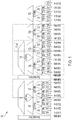
- FIG. 1 shows the 5 GHz WiFi band 100, which may include WiFi channels with bandwidths depending on the protocols used to access the channels.
- channels on the first row e.g., channels 36, 100, 149 with center frequencies 5180 MHz, 5500 MHz and 5745 MHz respectively
- channels on the second row e.g., channels 38, 102, 151 with center frequencies 5190 MHz, 5510 MHz and 5755 MHz respectively
- channels on the third row e.g., channels 42, 106, 155 with center frequencies 5210 MHz, 5530 MHz and 5775 MHz respectively
- channels on the fourth row e.g., channels 50, 114 with center frequencies 5250 MHz and 5570 MHz respectively
- channels on the fourth row e.g., channels 50, 114 with center frequencies 5250 MHz and 5570 MHz respectively
- WiFi channels may also be available to be occupied by a radar signal and referred to as radar-WiFi DFS co-channels (e.g., channels 52-144 on the first row, channels 54-142 on the second row, channels 58-138 on the third row, channels 50, 114 on the fourth row).
- DFS causes a WiFi transceiver to perform a Channel Availability Check (CAC), which determines the WiFi channels that are free of radar signals.
- CAC Channel Availability Check
- the WiFi transceivers may jump to one of the WiFi channels that are determined through CAC as free of radar signals.
- CAC Channel Availability Check
- a WiFi transceiver for DFS may include an IQ generator that provides orthogonal signals to a mixer.
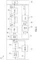
- FIG. 2 depicts a schematic diagram of a DFS receiver 200, according to some embodiments.
- the DFS receiver 200 may receive an RF input signal of a carrier frequency at an input node 202.
- the DFS receiver 200 may include a low noise amplifier (LNA) 204 configured to amplify the RF input signal while ensuring its signal-to-noise ratio.
- LNA low noise amplifier
- the illustrated LNA is a single-ended cascade LNA with integrated input matching and inductive source denegation, any suitable LNA may be employed.
- the DFS receiver 200 may include a test tone generator (TTG) 210 configured to generate a tone signal of the carrier frequency.
- TTG 210 may be coupled to a mixer 206 through a switch 216.
- the illustrated switch is connected to LNA output, any connecting points of LNA input may be employed.
- the illustrated mixer is a current-mode single-balanced passive I/Q mixer, any suitable mixer may be employed.
- the switch 216 may be turned on such that the tone signal generated by the TTG 210 may be used for calibration and to suppress sideband signals with respect to the carrier frequency. After the establishment of a WiFi link, the switch 216 may be turned off.
- the TTG 210 may be coupled to an IQ generator 208.
- the TTG 210 may send one or more of its outputs of the carrier frequency to the IQ generator 208.
- the IQ generator 208 may be configured to convert the outputs of the TTG 210 into orthogonal signals (e.g., I+, I-, Q+, Q-) and provide the orthogonal signals to the mixer 206.
- the DFS receiver 200 may include transimpedance amplifiers (TZA) and low pass filters (LPF) 212, which may be configured to drive successive-approximation-register (SAR) analog-to-digital converters (ADCs) 214.
- the TZA + LPF 212 may be configured with a fixed bandwidth (e.g., 80 MHz) such that the scan of the entire WiFi band may complete within a desired time (e.g., 6 minutes).
- a digital filter may divide the band detected with the radar signal into multiple bands with smaller bandwidths (e.g., an 80 MHz band may be divided into four 20 MHz bands). Then it is determined that the radar signal is in which one of the bands with smaller bandwidths. This configuration may save scan time.
- FIG. 3 is a block diagram of a portion 300 of a DFS receiver (e.g., the DFS receiver 200).
- the portion 300 of the DFS receiver may include an IQ generator 208 receiving an input from a TTG 210 and outputting to a mixer 206.
- the TTG 210 may include a ring oscillator 318, a buffer 320, and a feedback circuitry 322.
- the output signals 324 of the buffer 320 may be fed back to the oscillator 318 through the feedback circuitry 322.
- the feedback circuitry 322 may be configured to detect the phase and frequency of the output signals 324 and generate a control signal 332 for the oscillator 318 based on the detected phase and frequency of the output signals 324.
- the IQ generator 208 may be configured to receive the output signals 324 of the TTG 210.
- the IQ generator 208 may include a delay path 302 and a calibration circuitry 304.
- the delay path 302 may include a delay buffer 306, an IQ delay circuitry 308, a duty-cycle adjustment circuitry 310, and a mixer buffer 312.
- the IQ delay circuitry 308 may receive signals from the delay buffer 306 that may receive the output signals 324 of the TTG 210.
- the IQ delay circuitry 308 may be configured to generate IQ signals 326 that may be substantially orthogonal in phase.
- the IQ signals 326 may have a duty cycle that is similar to the duty cycle of the output signals 324 of the TTG 210, for example, a 50% duty cycle as illustrated.
- the duty-cycle adjustment circuitry 310 may be configured to modify the duty cycle of the IQ signals 326 to generate IQ signals 328.
- the IQ signals 328 may be amplified to IQ signals 330 by the mixer buffer 312, which may be provided to the mixer 206.
- the IQ signals 328 and 330 may have a duty cycle suitable for the mixer 206, and/or suitable for the calibration circuitry 304.
- the IQ signals 328 and 330 have a 25% duty cycle, which is reduced from the 50% duty cycle of the IQ signals 326.
- Providing, to the mixer 206 and the calibration circuitry 304, IQ signals with a 25% duty cycle may reduce signal overlapping for mixer operation.
- the calibration circuitry 304 may include a DC filter 314 and a low power comparator operational amplifier 316.
- the DC filter 314 may be configured to provide the average pulse widths (Vavg +/-) of the IQ signals 330 to the comparator 316.
- the comparator 316 may be configured to generate a control signal 336, which is provided to the IQ delay circuitry 308 such that the IQ delay circuitry 308 may adjust its transconductance to make IQ signals 330 within a targeted phase error.
- an IQ generator may receive as inputs differential outputs of a single phase of a TTG.
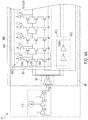
- FIGs. 4A , B depict a portion 400 of a DFS receiver, which may include an IQ generator 420 configured to receive as inputs differential outputs (e.g., IN, INb) of a single phase of a TTG 418 and provide IQ signals 422 to a mixer 426.
- FIG. 5 and FIG. 6 depict time diagrams of the TTG 418 and the IQ generator 420, according to some embodiments.
- the TTG 418 may produce multiple phase signals of a carrier frequency such as CK1, CK2, and CK3.
- the TTG 418 may have a differential configuration, and each phase signal may include a pair of differential signals (e.g., IN, INb for CK3).
- CK1 and CK3 may have a phase difference close to 90 degrees, these signals are likely to have large phase error, for example, illustrated as the shaded edges of CK1, CK2, and CK3 in FIG. 5 , and thus cannot provide a sufficient signal-to-noise ratio.
- the IQ generator 420 may be configured to generate IQ signals with low phase error, for example, illustrated as the sharp edges of I and Q in FIG. 5 .
- the IQ generator 420 may include a delay path 402 and a calibration circuitry 404.
- the delay path 402 may include a pair of delay buffers 406, configured to receive one of the pair of differential signals IN, INb, respectively.
- the delay path 402 may include a pair of I-delay circuitries 408A and 408B, configured to receive one of the outputs of the pair of delay buffers 406, respectively, and provide a pair of differential I signals (e.g., 50% I+, 50% I-, which may refer to a pair of differential I signals that has a duty cycle of 50%).
- the delay path 402 may include a pair of Q-delay circuitries 408C and 408D, configured to receive one of the outputs of the pair of delay buffers 406, respectively, and provide a pair of differential Q signals (e.g., 50% Q+, 50% Q-).
- a pair of differential Q signals e.g., 50% Q+, 50% Q-.
- One pair of the pair of I-delay circuitries 408A, 408B and the pair of Q-delay circuitries 408C, 408D may receive a control signal Vctrl, which may be configured to adjust the transconductance of the pair such that the IQ signals 422 are orthogonal in phase.
- each of the pair of I-delay circuitries 408A and 408B includes delay cells 424.
- a delay cell 424 may include a pair of transistors 424A, 424B sharing a same gate voltage, which may be an output of the pair of delay buffers 406 or an output of another delay cell.
- the delay cell 424 may include a pair of back-to-back connected inverters 424C, 424D coupled to an output of the pair of transistors 424A, 424B for phase matching.
- the delay cell 424 may include a delay unit 424E, which may be controlled by the control signal Vcrtl. Although the illustrated delay unit 424E has one transistor, a delay unit may include one or more transistors. Although five delay cells are illustrated, it should be appreciated either I or Q delay circuitry may include any suitable number of delay cells, for example, at least two delay cells. The number of delay cells may be selected depending on, for example, the carrier frequency. The higher the carrier frequency, the smaller the number of delay cells may be needed.
- the delay path 402 may include a duty-cycle adjustment circuitry 410 configured to receive the pairs of differential I signals (e.g., 50% I+, 50% I-) and different Q signals (e.g., 50% Q+, 50% Q-), modify the duty cycles of the pairs of differential I signals and different Q signals, and provide a new pair of differential I signals (e.g., 25% I+, 25% I-) and a new pair of differential Q signals (e.g., 25% Q+, 25% Q-).
- the duty-cycle adjustment circuitry 410 may include four NAND gates A-D configured to provide the new pair of differential I signals (e.g., 25% I+, 25% I-) and the new pair of differential Q signals (e.g., 25% Q+, 25% Q-).
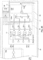
- the calibration circuitry 404 may be configured to generate the control signal Vcrtl that is fed back to the delay path 402.
- the calibration circuitry 404 may include a DC filter 414 and a low power comparator operational amplifier 416.
- the DC filter 414 may be configured to generate the average pulse width Vavg1 and the average pulse width Vavg2 of the new pair of I signals (e.g., 25% I+, 25% I-) and the new pair of differential Q signals (e.g., 25% Q+, 25% Q-), respectively.
- the low power comparator operational amplifier 416 may be configured to generate a control signal Vctrl based on the average pulse widths Vavg1 and Vavg2.
- the calibration circuitry 404 may modify the value of the control signal Vctrl until the average pulse widths Vavg1 and Vavg2 equal to each other.
- an IQ generator may receive as inputs multiple phase outputs of a TTG.
- FIG. 7 depicts a portion 700 of a DFS receiver, which may include an IQ generator 720 configured to receive as inputs multiple phase outputs of a TTG 718 (e.g., CK1, CK3) and provide IQ signals 722 to a mixer 706.
- FIG. 8 depict a time diagram of the IQ generator of FIG. 7 .
- the IQ generator 720 may include delay paths 7021, 702Q for respective phase outputs of the TTG 718.
- the delay paths 702I, 702Q may be configured to convert the multiple phase outputs of the TTG 718 into orthogonal signals (e.g., I, Q).
- the delay paths 7021, 702Q may be configured similar to the delay path 402 in FIGs. 4A , B.
- the delay paths of an IQ generator having multiple delay paths may include fewer delay cells than the delay path of an IQ generator having a single delay path.
- the IQ generator 720 may include a calibration circuitry 704, which may include a DC filter 714 and a comparator 716.
- the DC filter 714 may be configured to average pulse widths of the IQ signals, and/or generate a voltage V_comp representing a difference between the average pulse widths of the IQ signals.
- the comparator 716 may be configured to provide control signals Vt_I and Vt_Q to the delay paths 7021, 702Q, respectively, based on the output of the DC filter 714.
- the calibration circuitry 704 may modify the values of the control signals Vt_I and Vt_Q until the IQ signals have equal average pulse widths.
- IQ generators was described in connection with WiFi technology.
- IQ generators may be used in connection with any suitable technology.
- IQ generators may be used in connection with cellular technology.
- the terms “approximately”, “substantially,” and “about” may be used to mean within ⁇ 20% of a target value in some embodiments, within ⁇ 10% of a target value in some embodiments, within ⁇ 5% of a target value in some embodiments, and yet within ⁇ 2% of a target value in some embodiments.
Landscapes
- Engineering & Computer Science (AREA)
- Signal Processing (AREA)
- Computer Networks & Wireless Communication (AREA)
- Physics & Mathematics (AREA)
- Electromagnetism (AREA)
- Power Engineering (AREA)
- Nonlinear Science (AREA)
- Manipulation Of Pulses (AREA)
- Superheterodyne Receivers (AREA)
Abstract
Description
- This application claims priority to and the benefit of
U.S. Provisional Application Ser. No. 62/958,341, filed January 8, 2020 U.S. Non-Provisional Application Ser. No. 17/111,995, filed December 4, 2020 - This application relates generally to IQ generators.
- Wireless communication devices are commonly deployed in wireless communication systems to provide communication services such as voice, multimedia, data, broadcast, and messaging services. In a wireless communication device such as a mobile phone, an IQ generator may provide orthogonal signals represented by in-phase (I) and quadrature (Q) components.
- IQ generators with lower power consumption and smaller die area are provided.
- Some embodiment relates to a signal generator for generating signals that are orthogonal in phase. The signal generator comprises a delay path configured to generate the signals from an input signal of a carrier frequency, and a calibration circuitry configured to provide a control signal to the delay path based at least in part on the signals. An operating frequency of the signal generator is less than twice the carrier frequency.
- In some embodiments, the input signal of the carrier frequency is from a test tone generator.
- In some embodiments, the input signal of the carrier frequency comprises output signals of the test tone generator that are in two different phases.
- In some embodiments, the input signal of the carrier frequency comprises output signals of the test tone generator that are in a single phase.
- In some embodiments, the output signals of the test tone generator comprise a pair of differential signals in the single phase.
- In some embodiments, the delay path comprises one or more delay cells configured to adjust their transconductances based at least in part on the control signal from the calibration circuitry.
- In some embodiments, a delay cell of the one or more delay cells comprises a pair of transistors that receive the input signal of the carrier frequency, a back-to-back inverter coupled to the pair of transistors, and a delay unit connected in series with the pair of transistors and configured to adjust its transconductance based at least in part on the control signal from the calibration circuitry.
- In some embodiments, the calibration circuitry comprises a comparator configured to compare average pulse widths of the signals and provide the control signal based at least in part on the comparison.
- Some embodiment relates to a signal generator for generating signals that are orthogonal in phase. The signal generator comprises one or more delay paths comprising input nodes that receive an input signal of a carrier frequency and output nodes that provide the signals, and a calibration circuitry comprising input nodes that receive the signals and an output node that provides a control signal to the one or more delay paths. An operating frequency of the signal generator is less than twice the carrier frequency.
- In some embodiments, the input signal of the carrier frequency is from a test tone generator.
- In some embodiments, the input signal of the carrier frequency comprises a pair of differential signals in a single phase.
- In some embodiments, the one or more delay paths comprise a single delay path, and the output node of the calibration circuitry provides a respective control signal to the single delay path.
- In some embodiments, the single delay path comprises a plurality of delay cells controlled by the respective control signal.
- In some embodiments, the input signal of the carrier frequency has a 50% duty cycle, and the single delay path comprises a circuitry that receives signals with the 50% duty cycle and provides signals with a 25% duty cycle.
- In some embodiments, the input signal of the carrier frequency comprises a first output signal of the test tone generator that is in a first phase and a second output signal of the test tone generator that is in a second phase different from the first phase.
- In some embodiments, the one or more delay paths comprise a first delay path for the first output signal of the test tone generator and a second delay path for the second output signal of the test tone generator.
- In some embodiments, the output node of the calibration circuitry is a first output node of the calibration circuitry. The control signal is a first control signal. The first control signal is provided to the first delay path. The calibration circuitry comprises a second output node that provides a second control signal to the second delay path.
- In some embodiments, the calibration circuitry comprises a direct current (DC) filter comprising the input nodes of the calibration circuitry.
- Some embodiments relate to a receiver circuit. The receiver circuit comprises a low-noise amplifier configured to receive an input signal of a carrier frequency and amplify the input signal, a test tone generator configured to generate a tone signal of the carrier frequency, a signal generator configured to generate signals that are orthogonal in phase from the tone signal of the carrier frequency generated by the test tone generator, and a mixer configured to receive the amplified input signal and the signals.
- In some embodiments, the receiver circuit comprises a switch coupled between output nodes of the low-noise amplifier and the test tone generator. The switch is on when the tone signal of the carrier frequency is used to suppress sideband signals with respect to the carrier frequency.
- These techniques may be used alone or in any suitable combination. The foregoing summary is provided by way of illustration and is not intended to be limiting.
- The accompanying drawings are not intended to be drawn to scale. In the drawings, each identical or nearly identical component that is illustrated in various figures is represented by a like numeral. For purposes of clarity, not every component may be labeled in every drawing. In the drawings:
-
FIG. 1 is a schematic diagram of the 5 GHz WiFi band with WiFi channels and radar-WiFi dynamic frequency selection (DFS) co-channels shown. -
FIG. 2 is a schematic diagram of a DFS receiver, according to some embodiments. -
FIG. 3 is a block diagram of an IQ generator receiving an input from a test tone generator (TTG) and outputting to a mixer, according to some embodiments. -
FIGs. 4A , B are a schematic diagram of an IQ generator receiving as inputs multiple phase outputs of a TTG and outputting to a mixer, according to some embodiments. -
FIG. 5 is a time diagram of the TTG and the IQ generator ofFIGs. 4A , B, according to some embodiments. -
FIG. 6 is a time diagram of the TTG and the IQ generator ofFIGs. 4A , B, according to some embodiments. -
FIG. 7 is a schematic diagram of an IQ generator receiving as inputs differential outputs of a single phase of a TTG and outputting to a mixer, according to some embodiments. -
FIG. 8 is a time diagram of the TTG and the IQ generator ofFIG. 7 , according to some embodiments. - Described herein are IQ generators with lower power consumption and smaller die area. The inventors have recognized and appreciated that conventional IQ generators include a synthesizer operating at twice a carrier frequency and a divide-by-2 circuitry configured to convert an output of the synthesizer of the twice the carrier frequency into orthogonal signals of the carrier frequency. A synthesizer, for example, an LC-based voltage controlled oscillator (VCO), occupies significant die area, and increases cost of a chip that includes IQ generators. In addition to occupying extra chip area, the synthesizer and divide-by-2 circuitry, both of which are operating at twice the carrier frequency, consume significant power. This problem becomes more prominent when the carrier frequency increases, for example, to 6 GHz with 801.11ax or 801.11ac.
- The inventors have developed IQ generators with lower power consumption and smaller die area such that a synthesizer generating a signal of twice a carrier frequency is not needed. In some embodiments, IQ generators may be configured without any synthesizer and divide-by-2 circuitry.
- In some embodiments, an IQ generator may be configured to convert one or more phase outputs of a test tone generator into I and Q signals that are orthogonal in phase. In some embodiments, an IQ generator may receive as inputs differential outputs of a single phase of a test tone generator. In some embodiments, an IQ generator may receive as inputs multiple phase outputs of a test tone generator.
- In some embodiments, an IQ generator may include one or more delay paths configured to generate I and Q signals. In some embodiments, an IQ generator may include a single delay path configured to receive one of the differential outputs of the test tone generator. In some embodiments, an IQ generator may include multiple delay paths configured to receive respective phase outputs of the test tone generator. In some embodiments, each delay path may receive a respective control signal such that the I and Q signals generated are orthogonal in phase. In some embodiments, a delay path may include at least two delay cells configured to adjust their transconductances based on a control signal.
- In some embodiments, an IQ generator may include a calibration circuit configured to compare the average waveform bandwidths of the I and Q signals and provide one or more control signals to the one or more delay paths such that the I and Q signals are orthogonal in phase.
- IQ generators may be included in an application for Dynamic Frequency Selection (DFS). Pursuant to DFS, WiFi transceivers (e.g., n x n MIMO transceivers) may identify the presence of a co-channel radar signal so as to avoid such occupied channel when operating in frequency ranges that requires DFS including, for example, 5250-5350 and 5470-5725 MHz.
FIG. 1 shows the 5GHz WiFi band 100, which may include WiFi channels with bandwidths depending on the protocols used to access the channels. In the illustrated example, channels on the first row (e.g.,channels center frequencies 5180 MHz, 5500 MHz and 5745 MHz respectively) have a bandwidth of 20 MHz; channels on the second row (e.g.,channels center frequencies 5190 MHz, 5510 MHz and 5755 MHz respectively) have a bandwidth of 40 MHz; channels on the third row (e.g.,channels center frequencies 5210 MHz, 5530 MHz and 5775 MHz respectively) have a bandwidth of 80 MHz; and channels on the fourth row (e.g.,channels center frequencies 5250 MHz and 5570 MHz respectively) have a bandwidth of 160 MHz. Some of the WiFi channels may also be available to be occupied by a radar signal and referred to as radar-WiFi DFS co-channels (e.g., channels 52-144 on the first row, channels 54-142 on the second row, channels 58-138 on the third row,channels - A WiFi transceiver for DFS may include an IQ generator that provides orthogonal signals to a mixer.
FIG. 2 depicts a schematic diagram of aDFS receiver 200, according to some embodiments. TheDFS receiver 200 may receive an RF input signal of a carrier frequency at aninput node 202. TheDFS receiver 200 may include a low noise amplifier (LNA) 204 configured to amplify the RF input signal while ensuring its signal-to-noise ratio. Although the illustrated LNA is a single-ended cascade LNA with integrated input matching and inductive source denegation, any suitable LNA may be employed. - The
DFS receiver 200 may include a test tone generator (TTG) 210 configured to generate a tone signal of the carrier frequency. TheTTG 210 may be coupled to amixer 206 through aswitch 216. Although the illustrated switch is connected to LNA output, any connecting points of LNA input may be employed. Although the illustrated mixer is a current-mode single-balanced passive I/Q mixer, any suitable mixer may be employed. During the establishment of a WiFi link, theswitch 216 may be turned on such that the tone signal generated by theTTG 210 may be used for calibration and to suppress sideband signals with respect to the carrier frequency. After the establishment of a WiFi link, theswitch 216 may be turned off. - The
TTG 210 may be coupled to anIQ generator 208. TheTTG 210 may send one or more of its outputs of the carrier frequency to theIQ generator 208. TheIQ generator 208 may be configured to convert the outputs of theTTG 210 into orthogonal signals (e.g., I+, I-, Q+, Q-) and provide the orthogonal signals to themixer 206. - The
DFS receiver 200 may include transimpedance amplifiers (TZA) and low pass filters (LPF) 212, which may be configured to drive successive-approximation-register (SAR) analog-to-digital converters (ADCs) 214. In some embodiments, the TZA +LPF 212 may be configured with a fixed bandwidth (e.g., 80 MHz) such that the scan of the entire WiFi band may complete within a desired time (e.g., 6 minutes). When a radar signal is detected in any of the fixed bandwidth channels, a digital filter may divide the band detected with the radar signal into multiple bands with smaller bandwidths (e.g., an 80 MHz band may be divided into four 20 MHz bands). Then it is determined that the radar signal is in which one of the bands with smaller bandwidths. This configuration may save scan time. -
FIG. 3 is a block diagram of aportion 300 of a DFS receiver (e.g., the DFS receiver 200). Theportion 300 of the DFS receiver may include anIQ generator 208 receiving an input from aTTG 210 and outputting to amixer 206. TheTTG 210 may include aring oscillator 318, abuffer 320, and afeedback circuitry 322. The output signals 324 of thebuffer 320 may be fed back to theoscillator 318 through thefeedback circuitry 322. Thefeedback circuitry 322 may be configured to detect the phase and frequency of the output signals 324 and generate acontrol signal 332 for theoscillator 318 based on the detected phase and frequency of the output signals 324. - The
IQ generator 208 may be configured to receive the output signals 324 of theTTG 210. TheIQ generator 208 may include adelay path 302 and acalibration circuitry 304. Thedelay path 302 may include adelay buffer 306, anIQ delay circuitry 308, a duty-cycle adjustment circuitry 310, and amixer buffer 312. TheIQ delay circuitry 308 may receive signals from thedelay buffer 306 that may receive the output signals 324 of theTTG 210. TheIQ delay circuitry 308 may be configured to generateIQ signals 326 that may be substantially orthogonal in phase. The IQ signals 326 may have a duty cycle that is similar to the duty cycle of the output signals 324 of theTTG 210, for example, a 50% duty cycle as illustrated. - The duty-
cycle adjustment circuitry 310 may be configured to modify the duty cycle of the IQ signals 326 to generate IQ signals 328. The IQ signals 328 may be amplified toIQ signals 330 by themixer buffer 312, which may be provided to themixer 206. The IQ signals 328 and 330 may have a duty cycle suitable for themixer 206, and/or suitable for thecalibration circuitry 304. In the illustrated example, the IQ signals 328 and 330 have a 25% duty cycle, which is reduced from the 50% duty cycle of the IQ signals 326. Providing, to themixer 206 and thecalibration circuitry 304, IQ signals with a 25% duty cycle may reduce signal overlapping for mixer operation. - The
calibration circuitry 304 may include aDC filter 314 and a low power comparatoroperational amplifier 316. TheDC filter 314 may be configured to provide the average pulse widths (Vavg +/-) of the IQ signals 330 to thecomparator 316. Thecomparator 316 may be configured to generate acontrol signal 336, which is provided to theIQ delay circuitry 308 such that theIQ delay circuitry 308 may adjust its transconductance to makeIQ signals 330 within a targeted phase error. - In some embodiments, an IQ generator may receive as inputs differential outputs of a single phase of a TTG.
FIGs. 4A , B depict aportion 400 of a DFS receiver, which may include anIQ generator 420 configured to receive as inputs differential outputs (e.g., IN, INb) of a single phase of aTTG 418 and provideIQ signals 422 to amixer 426.FIG. 5 andFIG. 6 depict time diagrams of theTTG 418 and theIQ generator 420, according to some embodiments. - The
TTG 418 may produce multiple phase signals of a carrier frequency such as CK1, CK2, and CK3. In some embodiments, theTTG 418 may have a differential configuration, and each phase signal may include a pair of differential signals (e.g., IN, INb for CK3). Although some of the multiple phase signals such as CK1 and CK3 may have a phase difference close to 90 degrees, these signals are likely to have large phase error, for example, illustrated as the shaded edges of CK1, CK2, and CK3 inFIG. 5 , and thus cannot provide a sufficient signal-to-noise ratio. - The
IQ generator 420 may be configured to generate IQ signals with low phase error, for example, illustrated as the sharp edges of I and Q inFIG. 5 . TheIQ generator 420 may include adelay path 402 and acalibration circuitry 404. Thedelay path 402 may include a pair of delay buffers 406, configured to receive one of the pair of differential signals IN, INb, respectively. Thedelay path 402 may include a pair of I-delay circuitries delay path 402 may include a pair of Q-delay circuitries - One pair of the pair of I-
delay circuitries delay circuitries delay circuitries delay cells 424. Adelay cell 424 may include a pair oftransistors delay buffers 406 or an output of another delay cell. Thedelay cell 424 may include a pair of back-to-back connectedinverters 424C, 424D coupled to an output of the pair oftransistors delay cell 424 may include adelay unit 424E, which may be controlled by the control signal Vcrtl. Although the illustrateddelay unit 424E has one transistor, a delay unit may include one or more transistors. Although five delay cells are illustrated, it should be appreciated either I or Q delay circuitry may include any suitable number of delay cells, for example, at least two delay cells. The number of delay cells may be selected depending on, for example, the carrier frequency. The higher the carrier frequency, the smaller the number of delay cells may be needed. - The
delay path 402 may include a duty-cycle adjustment circuitry 410 configured to receive the pairs of differential I signals (e.g., 50% I+, 50% I-) and different Q signals (e.g., 50% Q+, 50% Q-), modify the duty cycles of the pairs of differential I signals and different Q signals, and provide a new pair of differential I signals (e.g., 25% I+, 25% I-) and a new pair of differential Q signals (e.g., 25% Q+, 25% Q-). The duty-cycle adjustment circuitry 410 may include four NAND gates A-D configured to provide the new pair of differential I signals (e.g., 25% I+, 25% I-) and the new pair of differential Q signals (e.g., 25% Q+, 25% Q-). In the illustrated example, the NAND gate A provides 25% I+ based on 50% I- and 50% Q+; the NAND gate B provides 25% I- based on 50% I+ and 50% Q-; the NAND gate C provides 25% Q+ based on 50% I+ and 50% Q+; the NAND gate D provides 25% Q- based on 50% I- and 50% Q-. - The
calibration circuitry 404 may be configured to generate the control signal Vcrtl that is fed back to thedelay path 402. Thecalibration circuitry 404 may include aDC filter 414 and a low power comparatoroperational amplifier 416. TheDC filter 414 may be configured to generate the average pulse width Vavg1 and the average pulse width Vavg2 of the new pair of I signals (e.g., 25% I+, 25% I-) and the new pair of differential Q signals (e.g., 25% Q+, 25% Q-), respectively. The low power comparatoroperational amplifier 416 may be configured to generate a control signal Vctrl based on the average pulse widths Vavg1 and Vavg2. Thecalibration circuitry 404 may modify the value of the control signal Vctrl until the average pulse widths Vavg1 and Vavg2 equal to each other. The equalization of the average pulse widths Vavg1 and Vavg2 enables that the IQ signals are orthogonal in phase as illustrated inFIG. 6 when T1=T2, compared with T1<T2 or T1>T2. - In some embodiments, an IQ generator may receive as inputs multiple phase outputs of a TTG.
FIG. 7 depicts aportion 700 of a DFS receiver, which may include anIQ generator 720 configured to receive as inputs multiple phase outputs of a TTG 718 (e.g., CK1, CK3) and provideIQ signals 722 to amixer 706.FIG. 8 depict a time diagram of the IQ generator ofFIG. 7 . - The
IQ generator 720 may includedelay paths TTG 718. Thedelay paths 702I, 702Q may be configured to convert the multiple phase outputs of theTTG 718 into orthogonal signals (e.g., I, Q). In some embodiments, thedelay paths delay path 402 inFIGs. 4A , B. In some embodiments, the delay paths of an IQ generator having multiple delay paths may include fewer delay cells than the delay path of an IQ generator having a single delay path. - The
IQ generator 720 may include acalibration circuitry 704, which may include aDC filter 714 and acomparator 716. TheDC filter 714 may be configured to average pulse widths of the IQ signals, and/or generate a voltage V_comp representing a difference between the average pulse widths of the IQ signals. Thecomparator 716 may be configured to provide control signals Vt_I and Vt_Q to thedelay paths DC filter 714. As thecalibration circuitry 404, thecalibration circuitry 704 may modify the values of the control signals Vt_I and Vt_Q until the IQ signals have equal average pulse widths. - Various changes may be made to the illustrative structures shown and described herein. For example, IQ generators was described in connection with WiFi technology. IQ generators may be used in connection with any suitable technology. As a specific example of a possible variation, IQ generators may be used in connection with cellular technology.
- Various aspects of the apparatus and techniques described herein may be used alone, in combination, or in a variety of arrangements not specially discussed in the embodiments described in the foregoing description and is therefore not limited in its application to the details and arrangement of components set forth in the foregoing description or illustrated in the drawings. For example, aspects described in one embodiment may be combined in any manner with aspects described in other embodiments.
- The terms "approximately", "substantially," and "about" may be used to mean within ±20% of a target value in some embodiments, within ±10% of a target value in some embodiments, within ±5% of a target value in some embodiments, and yet within ±2% of a target value in some embodiments.
- Use of ordinal terms such as "first," "second," "third," etc., in the claims to modify a claim element does not by itself connote any priority, precedence, or order of one claim element over another or the temporal order in which acts of a method are performed, but are used merely as labels to distinguish one claim element having a certain name from another element having a same name (but for use of the ordinal term) to distinguish the claim elements.
- Also, the phraseology and terminology used herein is for the purpose of description and should not be regarded as limiting. The use of "including," "comprising," or "having," "containing," "involving," and variations thereof herein, is meant to encompass the items listed thereafter and equivalents thereof as well as additional items.
Claims (15)
- A signal generator for generating signals that are orthogonal in phase, comprising:one or more delay paths (302, 402, 702I, 702Q) comprising input nodes (324, IN, INb) that receive an input signal of a carrier frequency and output nodes (330, 422, 722) that provide the signals; anda calibration circuitry (304, 404, 704) comprising input nodes that receive the signals and an output node that provides a control signal to the one or more delay paths, whereinan operating frequency of the signal generator is less than twice the carrier frequency.
- The signal generator of claim 1, wherein
the input signal of the carrier frequency is from a test tone generator (210, 418, 718). - The signal generator of any preceding claim, wherein
the input signal of the carrier frequency comprises a pair of differential signals in a single phase (IN, INb). - The signal generator of any preceding claim, wherein
the one or more delay paths comprise a single delay path (402), and
the output node of the calibration circuitry provides a control signal (Vctrl) to the single delay path. - The signal generator of claim 4, wherein
the single delay path comprises a plurality of delay cells (424) controlled by the control signal. - The signal generator of claim 4, wherein
the input signal of the carrier frequency has a 50% duty cycle, and
the single delay path comprises a circuitry (410) that receives signals with the 50% duty cycle and provides signals with a 25% duty cycle. - The signal generator of claim 2, wherein
the input signal of the carrier frequency comprises a first output signal of the test tone generator that is in a first phase and a second output signal of the test tone generator that is in a second phase different from the first phase. - The signal generator of claim 7, wherein
the one or more delay paths comprise a first delay path (7021) for the first output signal of the test tone generator and a second delay path (702Q) for the second output signal of the test tone generator. - The signal generator of claim 8, wherein
the output node of the calibration circuitry is a first output node of the calibration circuitry,
the control signal is a first control signal,
the first control signal (Vt_I) is provided to the first delay path, and
the calibration circuitry comprises a second output node that provides a second control signal (Vt_Q) to the second delay path. - The signal generator of any preceding claim, wherein
a delay path of the one or more delay path comprises one or more delay cells configured to adjust their transconductances based at least in part on the control signal from the calibration circuitry. - The signal generator of claim 10, wherein
a delay cell of the one or more delay cells comprisesa pair of transistors (424A, 424B) that receive the input signal of the carrier frequency,a back-to-back inverter (424C, 424D) coupled to the pair of transistors, anda delay unit (424E) connected in series with the pair of transistors and configured to adjust its transconductance based at least in part on the control signal from the calibration circuitry. - The signal generator of any preceding claim, wherein
the calibration circuitry comprises a comparator (316, 416, 716) configured to compare average pulse widths of the signals and provide the control signal based at least in part on the comparison. - The signal generator of any preceding claim, wherein
the calibration circuitry comprises a direct current (DC) filter (314, 414, 714) comprising the input nodes of the calibration circuitry. - A receiver circuit, comprising:a signal generator of any preceding claim;a test tone generator (210) configured to generate the input signal of the carrier frequency;a low-noise amplifier (204) configured to receive a second input signal (202) of a carrier frequency and amplify the second input signal; anda mixer (206) configured to receive the amplified second input signal and the signals that are orthogonal in phase.
- The receiver circuit of claim 14, comprising:a switch (216) coupled between output nodes of the low-noise amplifier and the test tone generator, whereinthe switch is on when the input signal of the carrier frequency is used to suppress sideband signals with respect to the carrier frequency.
Applications Claiming Priority (2)
| Application Number | Priority Date | Filing Date | Title |
|---|---|---|---|
| US202062958341P | 2020-01-08 | 2020-01-08 | |
| US17/111,995 US11646919B2 (en) | 2020-01-08 | 2020-12-04 | IQ generator for mixer |
Publications (2)
| Publication Number | Publication Date |
|---|---|
| EP3849107A1 true EP3849107A1 (en) | 2021-07-14 |
| EP3849107B1 EP3849107B1 (en) | 2025-04-16 |
Family
ID=74045403
Family Applications (1)
| Application Number | Title | Priority Date | Filing Date |
|---|---|---|---|
| EP20217977.6A Active EP3849107B1 (en) | 2020-01-08 | 2020-12-31 | Iq generator for mixer |
Country Status (4)
| Country | Link |
|---|---|
| US (1) | US11646919B2 (en) |
| EP (1) | EP3849107B1 (en) |
| CN (1) | CN113098400A (en) |
| TW (1) | TWI758060B (en) |
Families Citing this family (2)
| Publication number | Priority date | Publication date | Assignee | Title |
|---|---|---|---|---|
| US11973625B2 (en) * | 2021-11-22 | 2024-04-30 | Shenzhen GOODIX Technology Co., Ltd. | IQ clock phase calibration |
| US11742881B2 (en) * | 2022-01-10 | 2023-08-29 | Rockwell Collins, Inc. | Automatic phase shifting control loop |
Citations (3)
| Publication number | Priority date | Publication date | Assignee | Title |
|---|---|---|---|---|
| US20100246995A1 (en) * | 2003-09-29 | 2010-09-30 | Silicon Laboratories, Inc. | Method for Performing Dual Mode Image Rejection Calibration in a Receiver |
| EP2797234A1 (en) * | 2008-08-18 | 2014-10-29 | Qualcomm Incorporated | Local oscillator signal generator with automatic quadrature phase imbalance compensation |
| US10523220B1 (en) * | 2019-03-18 | 2019-12-31 | Avago Technologies International Sales Pte. Limited | Quadrature delay locked loops |
Family Cites Families (27)
| Publication number | Priority date | Publication date | Assignee | Title |
|---|---|---|---|---|
| JP2003168931A (en) * | 2001-12-04 | 2003-06-13 | Nec Corp | Distortion compensating circuit |
| CN100472941C (en) | 2003-04-24 | 2009-03-25 | 皇家飞利浦电子股份有限公司 | Quadrature modulator and its calibration method |
| GB2427089B (en) * | 2005-06-08 | 2009-11-25 | Zarlink Semiconductor Ltd | Radio frequency tuner |
| CN101233684B (en) * | 2005-10-17 | 2011-08-24 | 株式会社日立国际电气 | Non-linear distortion detection method and distortion compensation amplifying device |
| US7671691B2 (en) * | 2006-02-03 | 2010-03-02 | Anritsu Corporation | Quadrature modulator with phase controller apparatus and error detector |
| US7830954B2 (en) * | 2006-06-14 | 2010-11-09 | Broadcom Corporation | Method and apparatus for I/Q imbalance compensation |
| US7881402B2 (en) * | 2006-09-07 | 2011-02-01 | Via Technologies, Inc. | Compensation for gain imbalance, phase imbalance and DC offsets in a transmitter |
| JP5176692B2 (en) * | 2008-05-28 | 2013-04-03 | 日本電気株式会社 | Distortion compensation circuit and distortion compensation method |
| US8064848B2 (en) * | 2008-10-27 | 2011-11-22 | Mediatek Inc. | Transmitter and control method for transmitting and calibrating a phase signal and an amplitude signal |
| US8712357B2 (en) * | 2008-11-13 | 2014-04-29 | Qualcomm Incorporated | LO generation with deskewed input oscillator signal |
| US8350577B1 (en) * | 2010-04-19 | 2013-01-08 | Marvell Israel (M.I.S.L) Ltd. | Method and apparatus for calibration of pulse-width based measurement |
| CN102664608B (en) * | 2010-12-28 | 2015-03-11 | 博通集成电路(上海)有限公司 | Frequency multiplier and frequency multiplication method |
| US9479203B2 (en) * | 2011-04-14 | 2016-10-25 | Mediatek Inc. | Transceiver capable of IQ mismatch compensation on the fly and method thereof |
| JP5620590B2 (en) * | 2011-12-09 | 2014-11-05 | 株式会社Nttドコモ | Predistorter, predistorter control method |
| US10224908B1 (en) * | 2011-12-16 | 2019-03-05 | Altera Corporation | Low frequency variation calibration circuitry |
| US8660170B1 (en) * | 2012-12-09 | 2014-02-25 | Phuong Thu-Minh Huynh | Apparatus and method for calibrating the I/Q mismatch in a quadrature bandpass sampling receiver |
| US8687684B1 (en) * | 2012-12-18 | 2014-04-01 | Phuong Huynh | Apparatus and method for calibrating the I/Q mismatch in a quadrature bandpass sampling receiver |
| US9356732B2 (en) | 2013-03-15 | 2016-05-31 | Analog Devices, Inc. | Quadrature error detection and correction |
| US9176188B2 (en) | 2013-12-20 | 2015-11-03 | Texas Instruments Incorporated | Waveform calibration using built in self test mechanism |
| CN104734695B (en) * | 2013-12-24 | 2018-05-04 | 澜起科技(上海)有限公司 | Signal generator, electronic system and the method for producing signal |
| CN105141560B (en) * | 2015-07-16 | 2018-10-30 | 中国电子科技集团公司第四十一研究所 | A kind of multi-standard signal imitation device and method |
| CN107133014B (en) * | 2017-04-01 | 2021-02-12 | 中国人民解放军国防科技大学 | Broadband spectrum monitoring system and method for generating high-speed pseudo-random sequence signal |
| CN107432715B (en) * | 2017-09-08 | 2021-03-23 | 广东威灵电机制造有限公司 | Vacuum cleaner, motor and its control method and control device |
| US10958217B2 (en) | 2017-12-14 | 2021-03-23 | U-Blox Ag | Methods, circuits, and apparatus for calibrating an in-phase and quadrature imbalance |
| US10444785B2 (en) | 2018-03-15 | 2019-10-15 | Samsung Display Co., Ltd. | Compact and accurate quadrature clock generation circuits |
| CN110708084B (en) * | 2019-10-15 | 2022-04-29 | 成都振芯科技股份有限公司 | Envelope detection based originating IQ correction circuit and method |
| CN111404596B (en) * | 2020-03-27 | 2022-01-28 | 南京宽超通信技术有限公司 | Satellite downlink high-frequency head controller |
-
2020
- 2020-12-04 US US17/111,995 patent/US11646919B2/en active Active
- 2020-12-31 EP EP20217977.6A patent/EP3849107B1/en active Active
-
2021
- 2021-01-08 CN CN202110025756.1A patent/CN113098400A/en active Pending
- 2021-01-08 TW TW110100794A patent/TWI758060B/en active
Patent Citations (3)
| Publication number | Priority date | Publication date | Assignee | Title |
|---|---|---|---|---|
| US20100246995A1 (en) * | 2003-09-29 | 2010-09-30 | Silicon Laboratories, Inc. | Method for Performing Dual Mode Image Rejection Calibration in a Receiver |
| EP2797234A1 (en) * | 2008-08-18 | 2014-10-29 | Qualcomm Incorporated | Local oscillator signal generator with automatic quadrature phase imbalance compensation |
| US10523220B1 (en) * | 2019-03-18 | 2019-12-31 | Avago Technologies International Sales Pte. Limited | Quadrature delay locked loops |
Also Published As
| Publication number | Publication date |
|---|---|
| TW202131622A (en) | 2021-08-16 |
| US20210211335A1 (en) | 2021-07-08 |
| CN113098400A (en) | 2021-07-09 |
| TWI758060B (en) | 2022-03-11 |
| EP3849107B1 (en) | 2025-04-16 |
| US11646919B2 (en) | 2023-05-09 |
Similar Documents
| Publication | Publication Date | Title |
|---|---|---|
| US20100074303A1 (en) | Wireless Communication Apparatus | |
| US12124289B2 (en) | Multi-phase signal generation | |
| US11595003B2 (en) | Programmable driver for frequency mixer | |
| US11431358B2 (en) | Device and method for upconverting signal in wireless communication system | |
| US11881877B2 (en) | Spur compensation method and system | |
| EP3849107B1 (en) | Iq generator for mixer | |
| US20050239417A1 (en) | Transceiver circuit and method for providing local oscillator signals in a transceiver circuit | |
| Yang et al. | A parallel sliding-IF receiver front-end with sub-2-dB noise figure for 5–6-GHz WLAN carrier aggregation | |
| US20250300605A1 (en) | Transimpedance amplifier with virtual ground shunt resistor | |
| WO2025117167A1 (en) | Power amplifier with ruggedness and linearity improvement | |
| KR20180102640A (en) | Generate local oscillator signals in a wireless sensor device | |
| CN117795856A (en) | Local oscillator frequency divider with reduced applied current variation | |
| WO2021091616A1 (en) | Dual 3-phase harmonic rejection transceiver | |
| EP3868024A1 (en) | Downconversion using digital carrier signals | |
| US20250357896A1 (en) | Concurrent matching transceiver for power amplifier | |
| US20250038752A1 (en) | Calibration for a receiver by using neighboring receive paths | |
| US20250226822A1 (en) | Interleaved sampling circuit | |
| US20260088824A1 (en) | Phase alignment system and method | |
| US20250240038A1 (en) | Transmitter implemented with an inverter buffer | |
| HK40127951A (en) | Multi-phase signal generation | |
| WO2025029603A2 (en) | Calibration for a receiver by using neighboring receive paths | |
| US9391562B2 (en) | Local oscillation generator, associated communication system and method for local oscillation generation |
Legal Events
| Date | Code | Title | Description |
|---|---|---|---|
| PUAI | Public reference made under article 153(3) epc to a published international application that has entered the european phase |
Free format text: ORIGINAL CODE: 0009012 |
|
| STAA | Information on the status of an ep patent application or granted ep patent |
Free format text: STATUS: THE APPLICATION HAS BEEN PUBLISHED |
|
| AK | Designated contracting states |
Kind code of ref document: A1 Designated state(s): AL AT BE BG CH CY CZ DE DK EE ES FI FR GB GR HR HU IE IS IT LI LT LU LV MC MK MT NL NO PL PT RO RS SE SI SK SM TR |
|
| STAA | Information on the status of an ep patent application or granted ep patent |
Free format text: STATUS: REQUEST FOR EXAMINATION WAS MADE |
|
| 17P | Request for examination filed |
Effective date: 20220111 |
|
| RBV | Designated contracting states (corrected) |
Designated state(s): AL AT BE BG CH CY CZ DE DK EE ES FI FR GB GR HR HU IE IS IT LI LT LU LV MC MK MT NL NO PL PT RO RS SE SI SK SM TR |
|
| STAA | Information on the status of an ep patent application or granted ep patent |
Free format text: STATUS: EXAMINATION IS IN PROGRESS |
|
| 17Q | First examination report despatched |
Effective date: 20220401 |
|
| P01 | Opt-out of the competence of the unified patent court (upc) registered |
Effective date: 20230627 |
|
| GRAP | Despatch of communication of intention to grant a patent |
Free format text: ORIGINAL CODE: EPIDOSNIGR1 |
|
| STAA | Information on the status of an ep patent application or granted ep patent |
Free format text: STATUS: GRANT OF PATENT IS INTENDED |
|
| INTG | Intention to grant announced |
Effective date: 20241112 |
|
| GRAS | Grant fee paid |
Free format text: ORIGINAL CODE: EPIDOSNIGR3 |
|
| GRAA | (expected) grant |
Free format text: ORIGINAL CODE: 0009210 |
|
| STAA | Information on the status of an ep patent application or granted ep patent |
Free format text: STATUS: THE PATENT HAS BEEN GRANTED |
|
| AK | Designated contracting states |
Kind code of ref document: B1 Designated state(s): AL AT BE BG CH CY CZ DE DK EE ES FI FR GB GR HR HU IE IS IT LI LT LU LV MC MK MT NL NO PL PT RO RS SE SI SK SM TR |
|
| RAP3 | Party data changed (applicant data changed or rights of an application transferred) |
Owner name: MEDIATEK SINGAPORE PTE LTD |
|
| REG | Reference to a national code |
Ref country code: GB Ref legal event code: FG4D |
|
| REG | Reference to a national code |
Ref country code: CH Ref legal event code: EP Ref country code: DE Ref legal event code: R096 Ref document number: 602020049486 Country of ref document: DE |
|
| REG | Reference to a national code |
Ref country code: IE Ref legal event code: FG4D |
|
| REG | Reference to a national code |
Ref country code: NL Ref legal event code: MP Effective date: 20250416 |
|
| PG25 | Lapsed in a contracting state [announced via postgrant information from national office to epo] |
Ref country code: NL Free format text: LAPSE BECAUSE OF FAILURE TO SUBMIT A TRANSLATION OF THE DESCRIPTION OR TO PAY THE FEE WITHIN THE PRESCRIBED TIME-LIMIT Effective date: 20250416 |
|
| REG | Reference to a national code |
Ref country code: AT Ref legal event code: MK05 Ref document number: 1786538 Country of ref document: AT Kind code of ref document: T Effective date: 20250416 |
|
| PG25 | Lapsed in a contracting state [announced via postgrant information from national office to epo] |
Ref country code: PT Free format text: LAPSE BECAUSE OF FAILURE TO SUBMIT A TRANSLATION OF THE DESCRIPTION OR TO PAY THE FEE WITHIN THE PRESCRIBED TIME-LIMIT Effective date: 20250818 Ref country code: FI Free format text: LAPSE BECAUSE OF FAILURE TO SUBMIT A TRANSLATION OF THE DESCRIPTION OR TO PAY THE FEE WITHIN THE PRESCRIBED TIME-LIMIT Effective date: 20250416 Ref country code: ES Free format text: LAPSE BECAUSE OF FAILURE TO SUBMIT A TRANSLATION OF THE DESCRIPTION OR TO PAY THE FEE WITHIN THE PRESCRIBED TIME-LIMIT Effective date: 20250416 |
|
| REG | Reference to a national code |
Ref country code: LT Ref legal event code: MG9D |
|
| PG25 | Lapsed in a contracting state [announced via postgrant information from national office to epo] |
Ref country code: GR Free format text: LAPSE BECAUSE OF FAILURE TO SUBMIT A TRANSLATION OF THE DESCRIPTION OR TO PAY THE FEE WITHIN THE PRESCRIBED TIME-LIMIT Effective date: 20250717 Ref country code: NO Free format text: LAPSE BECAUSE OF FAILURE TO SUBMIT A TRANSLATION OF THE DESCRIPTION OR TO PAY THE FEE WITHIN THE PRESCRIBED TIME-LIMIT Effective date: 20250716 |
|
| PG25 | Lapsed in a contracting state [announced via postgrant information from national office to epo] |
Ref country code: PL Free format text: LAPSE BECAUSE OF FAILURE TO SUBMIT A TRANSLATION OF THE DESCRIPTION OR TO PAY THE FEE WITHIN THE PRESCRIBED TIME-LIMIT Effective date: 20250416 |
|
| PG25 | Lapsed in a contracting state [announced via postgrant information from national office to epo] |
Ref country code: BG Free format text: LAPSE BECAUSE OF FAILURE TO SUBMIT A TRANSLATION OF THE DESCRIPTION OR TO PAY THE FEE WITHIN THE PRESCRIBED TIME-LIMIT Effective date: 20250416 |
|
| PG25 | Lapsed in a contracting state [announced via postgrant information from national office to epo] |
Ref country code: HR Free format text: LAPSE BECAUSE OF FAILURE TO SUBMIT A TRANSLATION OF THE DESCRIPTION OR TO PAY THE FEE WITHIN THE PRESCRIBED TIME-LIMIT Effective date: 20250416 |
|
| PG25 | Lapsed in a contracting state [announced via postgrant information from national office to epo] |
Ref country code: AT Free format text: LAPSE BECAUSE OF FAILURE TO SUBMIT A TRANSLATION OF THE DESCRIPTION OR TO PAY THE FEE WITHIN THE PRESCRIBED TIME-LIMIT Effective date: 20250416 |
|
| PG25 | Lapsed in a contracting state [announced via postgrant information from national office to epo] |
Ref country code: RS Free format text: LAPSE BECAUSE OF FAILURE TO SUBMIT A TRANSLATION OF THE DESCRIPTION OR TO PAY THE FEE WITHIN THE PRESCRIBED TIME-LIMIT Effective date: 20250716 |
|
| PG25 | Lapsed in a contracting state [announced via postgrant information from national office to epo] |
Ref country code: IS Free format text: LAPSE BECAUSE OF FAILURE TO SUBMIT A TRANSLATION OF THE DESCRIPTION OR TO PAY THE FEE WITHIN THE PRESCRIBED TIME-LIMIT Effective date: 20250816 |
|
| PG25 | Lapsed in a contracting state [announced via postgrant information from national office to epo] |
Ref country code: LV Free format text: LAPSE BECAUSE OF FAILURE TO SUBMIT A TRANSLATION OF THE DESCRIPTION OR TO PAY THE FEE WITHIN THE PRESCRIBED TIME-LIMIT Effective date: 20250416 |
|
| PGFP | Annual fee paid to national office [announced via postgrant information from national office to epo] |
Ref country code: DE Payment date: 20251104 Year of fee payment: 6 |
|
| PGFP | Annual fee paid to national office [announced via postgrant information from national office to epo] |
Ref country code: GB Payment date: 20251114 Year of fee payment: 6 |
|
| PG25 | Lapsed in a contracting state [announced via postgrant information from national office to epo] |
Ref country code: DK Free format text: LAPSE BECAUSE OF FAILURE TO SUBMIT A TRANSLATION OF THE DESCRIPTION OR TO PAY THE FEE WITHIN THE PRESCRIBED TIME-LIMIT Effective date: 20250416 Ref country code: SM Free format text: LAPSE BECAUSE OF FAILURE TO SUBMIT A TRANSLATION OF THE DESCRIPTION OR TO PAY THE FEE WITHIN THE PRESCRIBED TIME-LIMIT Effective date: 20250416 |
|
| PGFP | Annual fee paid to national office [announced via postgrant information from national office to epo] |
Ref country code: FR Payment date: 20251110 Year of fee payment: 6 |
|
| REG | Reference to a national code |
Ref country code: DE Ref legal event code: R097 Ref document number: 602020049486 Country of ref document: DE |
|
| PG25 | Lapsed in a contracting state [announced via postgrant information from national office to epo] |
Ref country code: CZ Free format text: LAPSE BECAUSE OF FAILURE TO SUBMIT A TRANSLATION OF THE DESCRIPTION OR TO PAY THE FEE WITHIN THE PRESCRIBED TIME-LIMIT Effective date: 20250416 |
|
| PG25 | Lapsed in a contracting state [announced via postgrant information from national office to epo] |
Ref country code: EE Free format text: LAPSE BECAUSE OF FAILURE TO SUBMIT A TRANSLATION OF THE DESCRIPTION OR TO PAY THE FEE WITHIN THE PRESCRIBED TIME-LIMIT Effective date: 20250416 |
|
| PG25 | Lapsed in a contracting state [announced via postgrant information from national office to epo] |
Ref country code: RO Free format text: LAPSE BECAUSE OF FAILURE TO SUBMIT A TRANSLATION OF THE DESCRIPTION OR TO PAY THE FEE WITHIN THE PRESCRIBED TIME-LIMIT Effective date: 20250416 Ref country code: SK Free format text: LAPSE BECAUSE OF FAILURE TO SUBMIT A TRANSLATION OF THE DESCRIPTION OR TO PAY THE FEE WITHIN THE PRESCRIBED TIME-LIMIT Effective date: 20250416 |
|
| PG25 | Lapsed in a contracting state [announced via postgrant information from national office to epo] |
Ref country code: IT Free format text: LAPSE BECAUSE OF FAILURE TO SUBMIT A TRANSLATION OF THE DESCRIPTION OR TO PAY THE FEE WITHIN THE PRESCRIBED TIME-LIMIT Effective date: 20250416 |
|
| PLBE | No opposition filed within time limit |
Free format text: ORIGINAL CODE: 0009261 |
|
| STAA | Information on the status of an ep patent application or granted ep patent |
Free format text: STATUS: NO OPPOSITION FILED WITHIN TIME LIMIT |
|
| REG | Reference to a national code |
Ref country code: CH Ref legal event code: L10 Free format text: ST27 STATUS EVENT CODE: U-0-0-L10-L00 (AS PROVIDED BY THE NATIONAL OFFICE) Effective date: 20260225 |
|
| 26N | No opposition filed |
Effective date: 20260119 |