EP3848946A1 - Laminate of conductor and insulating film, coil, rotating electrical machine, insulating coating, and insulating film - Google Patents
Laminate of conductor and insulating film, coil, rotating electrical machine, insulating coating, and insulating film Download PDFInfo
- Publication number
- EP3848946A1 EP3848946A1 EP19857927.8A EP19857927A EP3848946A1 EP 3848946 A1 EP3848946 A1 EP 3848946A1 EP 19857927 A EP19857927 A EP 19857927A EP 3848946 A1 EP3848946 A1 EP 3848946A1
- Authority
- EP
- European Patent Office
- Prior art keywords
- laminate
- insulating coating
- insulating
- conductor
- metal oxide
- Prior art date
- Legal status (The legal status is an assumption and is not a legal conclusion. Google has not performed a legal analysis and makes no representation as to the accuracy of the status listed.)
- Pending
Links
Images



Classifications
-
- H—ELECTRICITY
- H01—ELECTRIC ELEMENTS
- H01B—CABLES; CONDUCTORS; INSULATORS; SELECTION OF MATERIALS FOR THEIR CONDUCTIVE, INSULATING OR DIELECTRIC PROPERTIES
- H01B7/00—Insulated conductors or cables characterised by their form
- H01B7/02—Disposition of insulation
- H01B7/0208—Cables with several layers of insulating material
- H01B7/0216—Two layers
-
- H—ELECTRICITY
- H01—ELECTRIC ELEMENTS
- H01B—CABLES; CONDUCTORS; INSULATORS; SELECTION OF MATERIALS FOR THEIR CONDUCTIVE, INSULATING OR DIELECTRIC PROPERTIES
- H01B3/00—Insulators or insulating bodies characterised by the insulating materials; Selection of materials for their insulating or dielectric properties
- H01B3/18—Insulators or insulating bodies characterised by the insulating materials; Selection of materials for their insulating or dielectric properties mainly consisting of organic substances
- H01B3/30—Insulators or insulating bodies characterised by the insulating materials; Selection of materials for their insulating or dielectric properties mainly consisting of organic substances plastics; resins; waxes
- H01B3/303—Macromolecular compounds obtained by reactions forming a linkage containing nitrogen with or without oxygen or carbon in the main chain of the macromolecule, not provided for in groups H01B3/38 or H01B3/302
- H01B3/306—Polyimides or polyesterimides
-
- H—ELECTRICITY
- H01—ELECTRIC ELEMENTS
- H01B—CABLES; CONDUCTORS; INSULATORS; SELECTION OF MATERIALS FOR THEIR CONDUCTIVE, INSULATING OR DIELECTRIC PROPERTIES
- H01B7/00—Insulated conductors or cables characterised by their form
- H01B7/02—Disposition of insulation
-
- C—CHEMISTRY; METALLURGY
- C09—DYES; PAINTS; POLISHES; NATURAL RESINS; ADHESIVES; COMPOSITIONS NOT OTHERWISE PROVIDED FOR; APPLICATIONS OF MATERIALS NOT OTHERWISE PROVIDED FOR
- C09D—COATING COMPOSITIONS, e.g. PAINTS, VARNISHES OR LACQUERS; FILLING PASTES; CHEMICAL PAINT OR INK REMOVERS; INKS; CORRECTING FLUIDS; WOODSTAINS; PASTES OR SOLIDS FOR COLOURING OR PRINTING; USE OF MATERIALS THEREFOR
- C09D179/00—Coating compositions based on macromolecular compounds obtained by reactions forming in the main chain of the macromolecule a linkage containing nitrogen, with or without oxygen, or carbon only, not provided for in groups C09D161/00 - C09D177/00
- C09D179/04—Polycondensates having nitrogen-containing heterocyclic rings in the main chain; Polyhydrazides; Polyamide acids or similar polyimide precursors
- C09D179/08—Polyimides; Polyester-imides; Polyamide-imides; Polyamide acids or similar polyimide precursors
-
- C—CHEMISTRY; METALLURGY
- C09—DYES; PAINTS; POLISHES; NATURAL RESINS; ADHESIVES; COMPOSITIONS NOT OTHERWISE PROVIDED FOR; APPLICATIONS OF MATERIALS NOT OTHERWISE PROVIDED FOR
- C09D—COATING COMPOSITIONS, e.g. PAINTS, VARNISHES OR LACQUERS; FILLING PASTES; CHEMICAL PAINT OR INK REMOVERS; INKS; CORRECTING FLUIDS; WOODSTAINS; PASTES OR SOLIDS FOR COLOURING OR PRINTING; USE OF MATERIALS THEREFOR
- C09D7/00—Features of coating compositions, not provided for in group C09D5/00; Processes for incorporating ingredients in coating compositions
- C09D7/40—Additives
- C09D7/60—Additives non-macromolecular
- C09D7/61—Additives non-macromolecular inorganic
-
- H—ELECTRICITY
- H01—ELECTRIC ELEMENTS
- H01B—CABLES; CONDUCTORS; INSULATORS; SELECTION OF MATERIALS FOR THEIR CONDUCTIVE, INSULATING OR DIELECTRIC PROPERTIES
- H01B3/00—Insulators or insulating bodies characterised by the insulating materials; Selection of materials for their insulating or dielectric properties
- H01B3/18—Insulators or insulating bodies characterised by the insulating materials; Selection of materials for their insulating or dielectric properties mainly consisting of organic substances
- H01B3/30—Insulators or insulating bodies characterised by the insulating materials; Selection of materials for their insulating or dielectric properties mainly consisting of organic substances plastics; resins; waxes
- H01B3/302—Polyurethanes or polythiourethanes; Polyurea or polythiourea
-
- H—ELECTRICITY
- H01—ELECTRIC ELEMENTS
- H01B—CABLES; CONDUCTORS; INSULATORS; SELECTION OF MATERIALS FOR THEIR CONDUCTIVE, INSULATING OR DIELECTRIC PROPERTIES
- H01B3/00—Insulators or insulating bodies characterised by the insulating materials; Selection of materials for their insulating or dielectric properties
- H01B3/18—Insulators or insulating bodies characterised by the insulating materials; Selection of materials for their insulating or dielectric properties mainly consisting of organic substances
- H01B3/30—Insulators or insulating bodies characterised by the insulating materials; Selection of materials for their insulating or dielectric properties mainly consisting of organic substances plastics; resins; waxes
- H01B3/308—Wires with resins
-
- H—ELECTRICITY
- H01—ELECTRIC ELEMENTS
- H01B—CABLES; CONDUCTORS; INSULATORS; SELECTION OF MATERIALS FOR THEIR CONDUCTIVE, INSULATING OR DIELECTRIC PROPERTIES
- H01B3/00—Insulators or insulating bodies characterised by the insulating materials; Selection of materials for their insulating or dielectric properties
- H01B3/18—Insulators or insulating bodies characterised by the insulating materials; Selection of materials for their insulating or dielectric properties mainly consisting of organic substances
- H01B3/30—Insulators or insulating bodies characterised by the insulating materials; Selection of materials for their insulating or dielectric properties mainly consisting of organic substances plastics; resins; waxes
- H01B3/42—Insulators or insulating bodies characterised by the insulating materials; Selection of materials for their insulating or dielectric properties mainly consisting of organic substances plastics; resins; waxes polyesters; polyethers; polyacetals
- H01B3/421—Polyesters
-
- H—ELECTRICITY
- H01—ELECTRIC ELEMENTS
- H01F—MAGNETS; INDUCTANCES; TRANSFORMERS; SELECTION OF MATERIALS FOR THEIR MAGNETIC PROPERTIES
- H01F27/00—Details of transformers or inductances, in general
- H01F27/28—Coils; Windings; Conductive connections
- H01F27/2823—Wires
-
- H—ELECTRICITY
- H01—ELECTRIC ELEMENTS
- H01F—MAGNETS; INDUCTANCES; TRANSFORMERS; SELECTION OF MATERIALS FOR THEIR MAGNETIC PROPERTIES
- H01F5/00—Coils
- H01F5/06—Insulation of windings
-
- C—CHEMISTRY; METALLURGY
- C08—ORGANIC MACROMOLECULAR COMPOUNDS; THEIR PREPARATION OR CHEMICAL WORKING-UP; COMPOSITIONS BASED THEREON
- C08K—Use of inorganic or non-macromolecular organic substances as compounding ingredients
- C08K3/00—Use of inorganic substances as compounding ingredients
- C08K3/18—Oxygen-containing compounds, e.g. metal carbonyls
- C08K3/20—Oxides; Hydroxides
- C08K3/22—Oxides; Hydroxides of metals
- C08K2003/2227—Oxides; Hydroxides of metals of aluminium
-
- C—CHEMISTRY; METALLURGY
- C08—ORGANIC MACROMOLECULAR COMPOUNDS; THEIR PREPARATION OR CHEMICAL WORKING-UP; COMPOSITIONS BASED THEREON
- C08K—Use of inorganic or non-macromolecular organic substances as compounding ingredients
- C08K3/00—Use of inorganic substances as compounding ingredients
- C08K3/18—Oxygen-containing compounds, e.g. metal carbonyls
- C08K3/20—Oxides; Hydroxides
- C08K3/22—Oxides; Hydroxides of metals
Definitions
- the present invention relates to a laminate of a conductor and an insulating coating, a coil, a rotating electric machine, an insulating paint, and an insulating film.
- Electric wires for use in electrical apparatuses such as motors include insulated electric wires on which an insulating layer is formed by applying to a conductor surface an insulating paint obtained by dissolving a resin such as a polyimide or polyamide-imide or a resin precursor thereof in an organic solvent, followed by baking; and insulated electric wires on which an insulating layer is formed by winding an insulating film such as a polyimide film or mica tape around a conductor (so-called tape wrapping).
- high voltage is applied to the insulated electric wires constituting coils. If microvoids are present between adjacent insulated electric wires or in the insulating coating, concentration of electric field may occur at that region, resulting in partial discharge. The partial discharge may cause deterioration of the insulating coating, which may cause premature dielectric breakdown of the coil, leading to a failure of the electrical apparatus.
- Methods for improving the electrical insulation lifetime against such partial discharge have been disclosed, such as a method in which an inorganic material formed of a metal oxide or the like is filled to prevent dielectric breakdown due to partial discharge; and a method in which a nano-size inorganic material is applied to achieve both partial discharge resistance and mechanical properties (flexibility and wear resistance) (see, for example, Patent Literatures 1 to 3).
- the present invention provides aspects of the invention comprising the following features:
- the present invention can provide a laminate of a conductor and an insulating coating that has excellent partial discharge resistance.
- the present invention can also provide a coil formed using the laminate as an electric wire, a rotating electric machine, and an insulating paint for forming the laminate.
- values connected with “to” refer to the numerical range including the values before and after "to” as the lower and upper limits.
- any lower limit and any upper limit may be selected and connected with "to”.
- the laminate of the present invention comprises at least a conductor and an insulating coating formed on the conductor.
- the insulating coating is formed of a resin composition containing a metal oxide hydrate, and an inorganic insulating layer is formed on the insulating coating when the laminate is exposed to partial discharge caused by inverter surges.
- the laminate of the present invention can exhibit excellent partial discharge resistance by virtue of these features.
- the laminate of the present invention also has less migration phenomenon and improved tracking resistance by virtue of these features.
- the laminate of the present invention will be hereinafter described in detail with reference to Figs. 1 to 16 .
- inverter surge refers to an abrupt overvoltage superimposed on the drive voltage, which occurs due to switching of an inverter.
- the switching frequency of an inverter ranges from a relatively low rate of about 1 kHz to a high rate of up to 100 kHz; hence, the frequency of occurrence of inverter surges is also extremely high, from about 1 to 100 kHz.
- the voltage ranges from a voltage of about 600 V that is superimposed on a drive voltage of 400 V for industrial inverter motors, to a voltage of about 3 kV that is superimposed on the drive voltage of high-voltage-driven inverter motors.
- a laminate 10 of the present invention includes a conductor 1 and an insulating coating 2.
- the laminate 10 of the present invention may be in the form of a film having at least the conductor 1 and the insulating coating 2 laminated on the conductor 1.
- the laminate 10 of the present invention may be in the form of an insulated electric wire having a conductor 1 at a central region and an insulating coating 2 formed around the perimeter of the conductor 1.
- the laminate 10 of the present invention may have a circular shape, an oval shape, a polygonal shape (which may be a straight angle shape or an irregular shape), or the like in cross section.
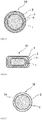
- Figs. 2 to 4 show insulated electric wires having a circular cross section.
- Fig. 5 shows an insulated electric wire having a generally rectangular cross section.
- the laminate 10 of the present invention includes at least the conductor 1 and the insulating coating 2, it may also include other layers.
- the other layers include, for example, insulating layers 3 and 4.
- Fig. 3 shows a laminate 10 (insulated electric wire) including a conductor 1, an insulating coating 2 formed around the conductor 1, and an insulating layer 3 formed around the insulating coating 2.
- Figs. 4 and 5 each show a laminate 10 (insulated electric wire) including a conductor 1, an insulating layer 4 formed around the conductor 1, an insulating coating 2 formed around the insulating layer 4, and an insulating layer 3 formed around the insulating coating 2.
- the materials constituting the insulating layers 3 and 4 may be, for example, the below-described resins having heat resistance (heat-resistant resins).
- the insulating layers 3 and 4 may each be formed of the same material as the material of the insulating coating 2, or may each be formed of other material.
- the insulating layers 3 and 4 may be formed of the same material or different materials.
- the insulating layers 3 and 4 may each be disposed under the insulating coating 2 (i.e., on the conductor 1 side), or may each be disposed over the insulating coating 2 (i.e., the side opposite to the conductor 1).
- the other layers also include a plating layer of a metal different from the conductor, which is formed between the conductor surface and an insulating layer.
- Fig. 10 shows, as another structure of the laminate 10 of the present invention, an insulated electric wire formed by winding around a conductor 1 an insulating film formed of a resin composition for forming an insulating coating 2.
- the insulating film can be formed by shaping the resin composition (insulating paint) for forming the insulating coating 2 using a film coater or the like, and baking the resin composition.
- This method of forming an insulated electric wire includes a method in which the insulating coating 2 is formed on the conductor; and a method in which an insulating film is formed independently and then wound around the conductor.
- the insulating film corresponds to the insulating coating 2 in the form of a film.
- the material constituting the conductor 1 may be any conductive material, for example, a metal such as copper (e.g., low-oxygen copper, oxygen-free copper, or a copper alloy), aluminum, silver, nickel, or iron.
- a metal such as copper (e.g., low-oxygen copper, oxygen-free copper, or a copper alloy), aluminum, silver, nickel, or iron.
- the material constituting the conductor 1 may be selected appropriately according to the purpose of the present invention.
- the insulating coating 2 is formed of a resin composition containing a resin and a metal oxide hydrate.
- the resin may be a highly heat-resistant resin, and may, for example, be a resin that is used for known insulated electric wires and the like.
- Specific examples of the resin include a formal resin, a polyurethane, an epoxy resin, a polyester, a polyamide, a polyester-imide, a polyetherimide, a polyamide-imide, a polyimide, and precursors thereof.
- a polyester-imide, a polyamide-imide, a polyimide, and a precursor of a polyimide are preferably used in order to improve the heat resistance.
- the polyimide may be an aromatic polyimide obtained by dehydration condensation of a known diamine and an acid anhydride.
- the known diamine include 4,4'-diaminodiphenyl ether
- examples of the acid anhydride include pyromellitic anhydride and biphenyltetracarboxylic dianhydride.
- the insulating coating 2 may contain a single resin or two or more resins as the resin.
- the resin may be used in the form of a solution or dispersion in a solvent (such as a resin varnish).
- a metal oxide hydrate is dispersed in the insulating paint used to form the insulating coating 2.
- the amount of the resin contained in the insulating coating 2 is preferably 50% by mass or more, and more preferably 60% by mass or more, while it is preferably 94% by mass or less, more preferably 90% by mass or less, and still more preferably 85% by mass or less, in order to allow an inorganic insulating layer 5 to be satisfactorily formed upon partial discharge to provide a laminate having improved partial discharge resistance.
- the metal oxide hydrate may be such that, after the insulating coating 2 of the laminate of the present invention is exposed to partial discharge, it forms the below-described inorganic insulating layer 5 on a portion of the region where the insulating coating 2 was previously formed.
- the metal oxide hydrate is preferably a hydrated alumina, which forms a particularly strong inorganic insulating layer 5.
- Examples of the hydrated alumina include trihydroxide (Al(OH) 3 ), and two variants of aluminum oxide hydroxide (AIO(OH)), i.e., boehmite ( ⁇ -aluminum oxide hydroxide) and diaspore ( ⁇ -aluminum oxide hydroxide).
- Boehmite is categorized into pseudo-crystalline boehmite and micro-crystalline boehmite, both of which can be used herein without limitation.
- a single metal oxide hydrate or two or more metal oxide hydrates may be used as the metal oxide hydrate.
- the inorganic insulating layer 5 is formed of at least one of a metal oxide and a metal oxide hydrate formed by partial dehydration of the metal oxide hydrate contained in the resin composition constituting the insulating coating 2.
- the metal oxide hydrate contained in the resin composition constituting the insulating coating 2 is Al(OH) 3
- examples of the metal oxide and the metal oxide hydrate formed by partial dehydration of the above-described metal oxide hydrate include Al(OH) 2 , AIO(OH), Al 2 O 3 , and mixtures thereof with Al(OH) 3 .
- the metal oxide hydrate is preferably contained in the form of fine particles in the insulating coating 2.
- the metal oxide hydrate is uniformly dispersed in the insulating coating 2, and preferably has a particle diameter of, for example, 100 nm or less.
- the metal oxide hydrate is preferably in the shape of flat fine particles having a high aspect ratio (one side/thickness), which facilitates forming the inorganic insulating layer 5, and the aspect ratio is preferably 4 to 200.
- the metal oxide hydrate is preferably uniformly dispersed with a nano-size in the insulating coating 2.
- the dispersed state of the metal oxide hydrate can be observed by TEM, and is preferably such that, for example, agglomerated particles with a particle diameter not less than 5 times the particle diameter of the metal oxide hydrate are not observed. The presence of such agglomerated particles may cause concentration of partial discharge at the agglomerated region, possibly leading to dielectric breakdown without the inorganic insulating layer 5 being formed.
- the nano-size refers to a dispersed particle diameter of 500 nm or less.
- the method of mixing the metal oxide hydrate and the resin is not limited as long as it allows the metal oxide hydrate to be uniformly dispersed in the insulating coating 2. It is, however, preferred to use a metal oxide hydrate sol.
- the use of a metal oxide hydrate sol facilitates uniformly dispersing the metal oxide hydrate in the insulating coating 2. If a metal oxide hydrate powder or gel is used, an agglomerate of the metal oxide hydrate may form in the insulating coating. This may cause concentration of partial discharge at the agglomerated region, possibly leading to dielectric breakdown without the inorganic insulating layer 5 being formed.
- the amount of the metal oxide hydrate contained in the insulating coating 2 is preferably 6 parts by mass or more, more preferably 10 parts by mass or more, and still more preferably 15 parts by mass or more, per 100 parts by mass of the resin, in order to allow the inorganic insulating layer 5 to be satisfactorily formed upon partial discharge to provide a laminate having improved partial discharge resistance.
- the upper limit of the amount of the metal oxide hydrate is preferably 100 parts by mass or less, and more preferably 70 parts by mass or less. If the amount of the metal oxide hydrate is less than 6 parts by mass, dielectric breakdown may possibly occur before the inorganic insulating layer 5 is formed. If the amount of the metal oxide hydrate is above 100 parts by mass, the insulating coating 2 may lose flexibility, possibly resulting in reduced flexibility.
- the resin be dissolved or dispersed in a solvent, and the metal oxide hydrate be dispersed in the solvent, in the insulating paint.
- the insulating coating 2 is formed by applying the insulating paint, followed by baking.
- High-boiling-point solvents are typically suitably used as the solvent, including cresol-based phenols, aromatic alcohols, NMP (N-methyl-2-pyrrolidone), DMAC (N,N-dimethylacetamide), DMF (N,N-dimethylformamide), DMI (1,3-dimethyl-2-imidazolidinone), carbonate-based solvents, lactone-based solvents, and glycol ether-based solvents.
- the insulating paint may contain a small amount of an acid component or an alkali component to stabilize the dispersion.
- the insulating paint may also contain water, a low-boiling-point alcohol, or a low-viscosity solvent or the like that contributes to reducing the viscosity of the insulating paint.
- the insulating paint may be mixed with other metal oxides or silicon oxides, or may contain a dispersant or a surface-treating agent added to impart hydrophobicity or improve the dispersibility.
- the inorganic insulating layer 5 is formed on a portion of the insulating coating 2. More specifically, as shown in the schematic diagrams of Figs. 6 and 7 , when the laminate 10 is exposed to partial discharge caused by inverter surges, the inorganic insulating layer 5 (21) is formed on a region 2a where partial discharge occurred in the insulating coating 2. In the region 2a where partial discharge occurred in the insulating coating 2, the insulating coating 2 is slightly eroded by partial discharge.
- the inorganic insulating layer 5 is formed, for example, on a portion of the side opposite to the conductor 1 side of the insulating coating 2.
- the laminate 10 of the present invention is a laminate 10 including at least the conductor 1, the insulating coating 2 formed on the perimeter of the conductor 1, and the inorganic insulating layer 5 formed on a portion of the side opposite to the conductor 1 side of the insulating coating 2.
- the laminate 10 of the present invention is a laminate 10 including at least the conductor 1, the insulating coating 2 formed on the perimeter of the conductor 1, the composite layer 6 formed on a portion of the side opposite to the conductor 1 side of the insulating coating 2, and the inorganic insulating layer 5 formed on a portion of the side opposite to the conductor 1 side of the composite layer 6.
- Fig. 7 is an enlarged schematic view of the region 2a where partial discharge occurred in the insulating coating 2, in the laminate 10 shown in Fig. 6 .
- the inorganic insulating layer 5 (21) is formed that is based on a metal oxide or a metal oxide hydrate formed by partial dehydration of the starting-material metal oxide hydrate contained in the insulating coating 2.
- Fig. 7 also shows that the composite layer 6 (22) is formed between the insulating coating 2 and the inorganic insulating layer 5.
- the composite layer 6 contains a mixture of the materials constituting the insulating coating 2 and the inorganic insulating layer 5.
- the composite layer 6 contains a mixture of the resin and the metal oxide hydrate contained in the insulating coating 2, and the metal oxide or the metal oxide hydrate formed by partial dehydration of the above-described metal oxide hydrate contained in the inorganic insulating layer 5.
- the proportion of the resin contained in the composite layer 6 is smaller than the proportion of the resin contained in the insulating coating 2.
- the composite layer 6 contains voids. The voids in the composite layer 6 are formed by the elimination of a portion of the resin due to partial discharge.
- the inorganic insulating layer 5 formed upon partial discharge is observed as a visually identifiable white layer, for example.
- the thickness of the inorganic insulating layer 5 is, for example, 10 nm or more, preferably 30 nm or more, and more preferably 50 nm or more.
- the electrical insulation lifetime is sharply increased. That is, the inorganic insulating layer 5 achieves a significant effect of acting as a barrier against partial discharge to prevent dielectric breakdown due to partial discharge.
- the inorganic insulating layer 5 is formed simultaneously with the elimination of the resin.
- the thickness of the inorganic insulating layer 5 varies with factors such as the amount of the resin eliminated by partial discharge, the amount of the metal oxide hydrate, and the designed thickness of the insulating coating 2 and the actually applied electric field strength.
- the upper limit of the thickness of the inorganic insulating layer 5 is, for example, 5 ⁇ m.
- the required thickness of the inorganic insulating layer 5 is determined by the actually applied electric field strength and the guaranteed lifetime of the electrical apparatus.
- the thickness is designed appropriately to achieve thicknesses of the insulating coating 2 and also the inorganic insulating layer 5 suitable for the type of the electrical apparatus.
- the inorganic insulating layer 5 may contain voids, and the void ratio of the inorganic insulating layer 5 is preferably lower than 20%. As the inorganic insulating layer 5 becomes denser with a void ratio lower than 20%, the effect of preventing dielectric breakdown due to partial discharge becomes more significant.
- the composite layer 6 is assumed to be a precursor phase to the formation of the inorganic insulating layer 5.
- the composite layer 6 is a layer having a void ratio higher than that of the inorganic insulating layer 5, and hence, can provide a high heat insulation effect. Therefore, a higher heat insulation effect is expected with increasing thickness of the composite layer 6.
- the void ratio of the composite layer 6 is preferably 20% or more, and more preferably 30% or more.
- the upper limit of the void ratio of the composite layer 6 is 80%, for example.
- the thickness of the composite layer 6 is, for example, 10 nm or more, preferably 50 nm or more, and more preferably 100 nm or more. When the thickness of the composite layer 6 is 10 nm or more, the heat insulation effect becomes higher, and dielectric breakdown is further prevented. This can markedly increase the electrical insulation lifetime, in combination with the partial discharge resistance imparted by the inorganic insulating layer 5.
- Figs. 8 and 9 are each a schematic cross-sectional view showing the state of an insulating coating 200 after partial discharge occurred (dielectric breakdown region) in a conventional insulated electric wire 100.
- the insulating coating 200 formed of a resin is formed, and a dielectric breakdown region 7 is formed upon partial discharge, resulting in significantly reduced insulating properties.
- the dielectric breakdown region 7 penetrates the insulating coating 200, exposing the surface of the conductor 1 to the outside.
- the inorganic insulating layer 5 and the composite layer 6 are not formed.
- the laminate 10 of the present invention can be produced by laminating at least the insulating coating 2 on the conductor 1.
- the insulating coating 2 can be formed by applying the above-described insulating paint containing a resin and a metal oxide hydrate, followed by baking.
- the insulating paint for forming the insulating coating 2 is applied on the surface of the conductor 1 and baked to form the insulating coating 2.
- Examples of methods of applying the insulating paint include a method in which the insulating paint is applied with a coater; a method in which the insulting paint is repeatedly applied and dried with a dip coater or a die to obtain a coating with a predetermined thickness; and spray coating.
- Baking may be performed by heating at a high temperature (for example, 300°C or more) for a predetermined time.
- the insulating coating 2 may also be formed by repeating a series of application and heating operations a plurality of times until a predetermined thickness of the insulating coating 2 is achieved. The baking temperature and time are adjusted according to the type of the metal oxide hydrate, such that the metal oxide hydrate does not alter to another metal oxide hydrate or metal oxide.
- the inorganic insulating layer 5 of the present invention is formed on a portion of the insulating coating 2 when the laminate is exposed to partial discharge caused by inverter surges. This partial discharge occurs, for example, at a frequency of 1 to 100 kHz and a voltage of 600 V to 3 kV.
- the insulated electric wire can be produced by applying the insulating paint onto the perimeter of the conductor 1 or onto another layer that covers the perimeter of the conductor 1, followed by baking.
- the insulating coating 2 can be formed by repeating a plurality of times (for example, 10 to 20 times) a series of operations (application and heating) of applying the insulating paint onto the perimeter of the conductor 1 at a predetermined thickness, and heating at a high temperature (for example, from 300 to 500°C or more) for a predetermined time (for example, 1 to 2 minutes), until a predetermined thickness of the insulating coating 2 is achieved.
- the coil of the present invention can be formed by winding the above-described insulated electric wire around a core.
- the rotating electric machine of the present invention is a rotating electric machine in which the coil of the present invention is used for a motor or the like. That is, the rotating electric machine of the present invention may be produced using the insulated electric wire of the present invention, or may be produced by forming a rotating electric machine using the conductor 1, and then forming the insulating coating 2 on the surface of the conductor 1 to form an electric wire.
- Examples of the rotating electric machine include motors and generators.
- the laminate of the present invention can be used as a flexible circuit board or an acoustic member.
- flexible circuit boards include flexible printed circuit boards.
- the flexible circuit board can be produced by applying the insulating paint onto the surface of a conductor or onto another layer that covers the surface of a conductor, followed by baking.
- acoustic members include resin films for speaker diaphragms.
- UPIA registered trademark
- U-varnish-A U-varnish-A
- Neoheat 8600 available from Totoku Toryo Co., Ltd. was used.
- Insulating paints each having the composition shown in Table 1 were produced as described below.
- the polyamide-imide paint 1 was mixed with 20 parts by mass of flat particles of an aluminum hydroxide (Al(OH) 3 ) (average particle diameter: 30 nm, thickness: about 1 to 5 nm, aspect ratio (one side/thickness): 6 to 30) as a hydrated alumina, relative to 80 parts by mass of the resin, and the aluminum hydroxide was uniformly dispersed to obtain an insulating paint.
- Al(OH) 3 aluminum hydroxide
- a sol previously prepared by dispersing the aluminum hydroxide in NMP solvent was used during mixing.
- the polyester-imide paint was mixed with 20 parts by mass of flat particles of an aluminum hydroxide (Al(OH) 3 ) (average particle diameter: 100 nm, thickness: about 2 to 5 nm, aspect ratio (one side/thickness): 20 to 50) as a hydrated alumina, relative to 80 parts by mass of the resin, and the aluminum hydroxide was uniformly dispersed to obtain an insulating paint.
- Al(OH) 3 aluminum hydroxide
- a sol previously prepared by dispersing the aluminum hydroxide in a solvent mixture of a meta/para-cresol mixture and an aromatic hydrocarbon was used during mixing.
- the polyimide paint 1 was mixed with 20 parts by mass of rectangular flat particles of boehmite (particle diameter: about 10 nm ⁇ 50 nm, thickness: about 1 to 5 nm, aspect ratio (long side/thickness): 10 to 50) as a hydrated alumina, relative to 80 parts by mass of the resin, and the boehmite was uniformly dispersed to obtain an insulating paint.
- a sol previously prepared by dispersing the boehmite in NMP was used during mixing.
- phosphoric acid ethyl ester ethyl acid phosphate (Ethyl Phosphate(Mono- and Di- Ester mixture) available from Tokyo Chemical Industry Co., Ltd.; monoester content: 35.0 to 47.0%; diester content: 53.0 to 67.0%)
- phosphoric acid ethyl ester ethyl acid phosphate (Ethyl Phosphate(Mono- and Di- Ester mixture) available from Tokyo Chemical Industry Co., Ltd.; monoester content: 35.0 to 47.0%; diester content: 53.0 to 67.0%)
- the polyimide paint 1 was mixed with 20 parts by mass of flat particles of boehmite (average particle diameter: 20 nm, thickness: about 1 to 5 nm, aspect ratio (one side/thickness): 4 to 20) as a hydrated alumina treated with a methacrylic silane coupling agent (KBM-503; Shin-Etsu Silicone), relative to 80 parts by mass of the resin, and the boehmite was uniformly dispersed to obtain an insulating paint.
- a sol previously prepared by dispersing the boehmite in a solvent mixture of ethanol and NMP was used during mixing. To prevent gelling, the boehmite sol was adjusted to have an ethanol-to-NMP ratio of 40 to 60 parts by mass.
- the polyamide-imide paint was mixed with 10 parts by mass of rectangular flat particles of boehmite (particle diameter: about 10 nm ⁇ 50 nm, thickness: about 1 to 5 nm, aspect ratio (long side/thickness): 10 to 50) as a hydrated alumina, relative to 90 parts by mass of the resin, and the boehmite was uniformly dispersed to obtain an insulating paint.
- phosphoric acid ethyl ester ethyl acid phosphate (Ethyl Phosphate(Mono- and Di- Ester mixture) available from Tokyo Chemical Industry Co., Ltd.; monoester content: 35.0 to 47.0%; diester content: 53.0 to 67.0%)
- monoester content: 35.0 to 47.0%; diester content: 53.0 to 67.0% was added to the boehmite sol.
- An insulating paint was obtained as in Example 3, except that the polyimide paint 1 was replaced by the polyimide paint 2.
- An insulating paint was obtained as in Example 3, except that the polyimide paint 1 was replaced by the polyimide paint 3.
- An insulating paint was obtained as in Example 3, except that the polyimide paint 1 was mixed with 15 parts by mass of the hydrated alumina, relative to 85 parts by mass of the resin.
- the insulating paint was applied to a copper conductor (diameter: about 1 mm), and baked for about 1 minute while the temperature was continuously increased from an inlet temperature of 350°C to an outlet temperature of 420°C. This process was repeated to produce an electric wire having a 38- ⁇ m-thick insulating coating (hydrated alumina concentration: 15% by mass) on the surface of the copper conductor (diameter: about 1 mm).
- the polyamide-imide paint 1 was mixed with 20 parts by mass of spherical particles of alumina (average particle diameter: 20 nm), relative to 80 parts by mass of the resin, and the alumina was uniformly dispersed to obtain an insulating paint.
- a sol previously prepared by dispersing the alumina in NMP was used during mixing.
- the polyimide paint 1 was mixed with 20 parts by mass of silica (average particle diameter: 13 nm, spherical), relative to 80 parts by mass of the resin, and the silica was uniformly dispersed to obtain an insulating paint.
- a silica sol previously prepared by dispersing the silica in NMP was used during mixing.
- the polyimide paint 1 was mixed with talc particles (average particle diameter: 0.6 ⁇ m, plate-like) to give 20 parts by mass of talc, relative to 80 parts by mass of the resin, and the talc particles were uniformly dispersed to obtain an insulating paint.
- talc particles average particle diameter: 0.6 ⁇ m, plate-like
- the polyimide paint 1 was mixed with zinc oxide fine particles (average particle diameter: 35 nm, spherical) to give 20 parts by mass of the zinc oxide, relative to 80 parts by mass of the resin, and the zinc oxide fine particles were uniformly dispersed to obtain an insulating paint.
- zinc oxide fine particles average particle diameter: 35 nm, spherical
- An insulating paint was obtained as in Example 2, except that the aluminum hydroxide was not used.
- An insulating paint was obtained as in Example 1, except that the aluminum hydroxide was not used.
- An insulating paint was obtained as in Example 3, except that the boehmite was not used.
- An insulating paint obtained as in Comparative Example 7 was applied to a copper conductor (diameter: about 1 mm), and baked for about 1 minute while the temperature was continuously increased from an inlet temperature of 350°C to an outlet temperature of 420°C. This process was repeated to produce an electric wire having a 38- ⁇ m-thick insulating coating on the surface of the copper conductor (diameter: about 1 mm).
- the polyester-imide paint was mixed with 20 parts by mass of silica (average particle diameter: 13 nm, spherical), relative to 80 parts by mass of the resin, and the silica was uniformly dispersed to obtain an insulating paint.
- a silica sol previously prepared by dispersing the silica in NMP was used during mixing.
- the insulating paint was applied to a copper conductor, and baked for about 1 minute while the temperature was continuously increased from an inlet temperature of 350°C to an outlet temperature of 420°C. This process was repeated to produce an electric wire having a 38- ⁇ m-thick insulating coating (silica concentration: 15% by mass) on the surface of the copper conductor (diameter: about 1 mm).
- Laminates (films) of conductors and insulating coatings were produced using the insulating paints obtained in Examples 1 to 7 and Comparative Examples 1 to 7. Specifically, each insulating paint was uniformly applied to the surface of aluminum foil (thickness: 300 ⁇ m) serving as a conductor, and baked at a temperature of 300°C for 1 hour to obtain a film having an insulating coating (thickness: 50 ⁇ m) laminated on the surface of the aluminum foil.
- a partial discharge exposure test and a V-t characteristic evaluation were conducted using the method described below.
- a voltage was applied across an electrode and each film, using a rod electrode.
- the testing method was as follows: As shown in Fig. 15 , sequentially from below, on a stainless steel support 23, an aluminum sheet 1 covered with the insulating coating 2 was mounted. A metal ball 22 (2 mm in diameter) and a copper tube 21 were sequentially placed thereon, and fixed to press under their own weight.
- the copper tube 21 and the aluminum sheet (conductor 1) were connected to a power supply, such that the metal ball 22 served as a high-voltage electrode and the aluminum sheet (conductor 1) as a low-voltage electrode.
- the voltage was applied by generating bipolar square waves at a pulse width of 5 ⁇ s and a frequency of 10 kHz, using the inverter pulse generator PG-W03KP-A available from Nissin Pulse Electronics Co., Ltd.
- V-t characteristic evaluation voltage-partial discharge lifetime characteristic test
- a twisted pair sample was produced in accordance with JIS C 3216, and a voltage was applied across the two wires.
- the voltage was applied by generating bipolar square waves at a pulse width of 5 ⁇ s and a frequency of 10 kHz, using the inverter pulse generator PG-W03KP-A available from Nissin Pulse Electronics Co., Ltd.
- a (visual) test for the presence/absence of the inorganic insulating layer involved visually observing an eroded region after the V-t test at 1.5 kVp.
- a (visual) test for the presence/absence of the inorganic layer after tape peel test involved carrying out a tape peel test in accordance with JIS H 8504 on the eroded region of the sample after the (visual) test for the presence/absence of the inorganic insulating layer, and visually observing the sample after the test.
- the thicknesses of the inorganic insulating layer and the composite layer were measured by continuously applying a voltage of 2.0 kVp for 100 hours, embedding a partial discharge-induced eroded region of the coating in resin, cutting the cross section into thin pieces by FIB (gallium focused ion beam), checking the presence/absence of the inorganic insulating layer and the composite layer by TEM (transmission electron microscopy), and then measuring the thicknesses of the layers. The results are shown in Table 1.
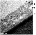
- Fig. 11 is a TEM image of a region where partial discharge occurred in the insulating coating of Example 3.
- the layer structure as shown in the enlarged schematic view shown in Fig. 7 was observed.
- the white regions shown in the image indicate voids.
- Fig. 12 is an enlarged TEM image of the inorganic insulating layer 5, the composite layer 6, or the insulating coating 2 in sequence from the left, in the image shown in Fig. 11 .
- the inorganic insulating layer 5 is a very dense layer, and the crystals of the inorganic particles are joined together, since each one of the crystals is not seen.
- the composite layer 6 is a layer in which voids, the metal oxide hydrate fine particles, and the remaining heat-resistant resin are combined.
- the metal oxide hydrate fine particles are randomly dispersed in the heat-resistant resin, as in the insulating coating 2 before exposure to partial discharge.
- staining was performed using image processing to determine the void ratio of the composite layer 6 formed in the film of Example 3, and the ratio of the area of voids P to the area of the whole composite layer 6 was determined. As a result of the calculation, the void ratio of the composite layer 6 was about 42%. Using the same technique, the void ratio of the inorganic insulating layer 5 formed in the film of Example 3 was also determined. As a result, the void ratio was about 5%.
- Fig. 14 is a TEM image of a region where partial discharge occurred in the insulating coating of Comparative Example 2. It can be observed that although the inorganic insulating layer 5 is observable, it contains many voids, and is very sparse. It can also be seen that the inorganic insulating layer 5 has numerous defective regions on the surface, and is fragile.
Landscapes
- Chemical & Material Sciences (AREA)
- Engineering & Computer Science (AREA)
- Power Engineering (AREA)
- Spectroscopy & Molecular Physics (AREA)
- Physics & Mathematics (AREA)
- Life Sciences & Earth Sciences (AREA)
- Materials Engineering (AREA)
- Wood Science & Technology (AREA)
- Organic Chemistry (AREA)
- Inorganic Chemistry (AREA)
- Chemical Kinetics & Catalysis (AREA)
- Organic Insulating Materials (AREA)
- Insulated Conductors (AREA)
- Laminated Bodies (AREA)
- Insulating Bodies (AREA)
- Paints Or Removers (AREA)
- Inorganic Insulating Materials (AREA)
Abstract
Description
- The present invention relates to a laminate of a conductor and an insulating coating, a coil, a rotating electric machine, an insulating paint, and an insulating film.
- Electric wires for use in electrical apparatuses such as motors include insulated electric wires on which an insulating layer is formed by applying to a conductor surface an insulating paint obtained by dissolving a resin such as a polyimide or polyamide-imide or a resin precursor thereof in an organic solvent, followed by baking; and insulated electric wires on which an insulating layer is formed by winding an insulating film such as a polyimide film or mica tape around a conductor (so-called tape wrapping).
- In electrical apparatuses with a high operating voltage, such as motors used at a high voltage, high voltage is applied to the insulated electric wires constituting coils. If microvoids are present between adjacent insulated electric wires or in the insulating coating, concentration of electric field may occur at that region, resulting in partial discharge. The partial discharge may cause deterioration of the insulating coating, which may cause premature dielectric breakdown of the coil, leading to a failure of the electrical apparatus.
- Furthermore, in recent years, even in apparatuses categorized as the low-voltage-driven type of systems in which motors or the like are driven by inverters used for energy conservation and variable speed, there has been an increasing number of cases where abrupt overvoltages (so-called inverter surges) occur in the drive voltage repeatedly in an extremely short period, leading to dielectric breakdown. The dielectric breakdown is due to partial discharge caused by the overvoltages that occur repeatedly due to the inverter surges.
- Methods for improving the electrical insulation lifetime against such partial discharge have been disclosed, such as a method in which an inorganic material formed of a metal oxide or the like is filled to prevent dielectric breakdown due to partial discharge; and a method in which a nano-size inorganic material is applied to achieve both partial discharge resistance and mechanical properties (flexibility and wear resistance) (see, for example,
Patent Literatures 1 to 3). -
- Patent Literature 1:
US Patent No. 5,654,095 - Patent Literature 2:
JP 2006-302835 A - Patent Literature 3:
JP 2001-307557 A - It is a main object of the present invention to provide a laminate of a conductor and an insulating coating that has excellent partial discharge resistance. It is also an object of the present invention to provide a coil formed using the laminate as an insulated electric wire, a rotating electric machine, an insulating paint for forming the laminate, and an insulating film.
- The present invention provides aspects of the invention comprising the following features:
-
Item 1. A laminate comprising at least a conductor and an insulating coating, wherein
the insulating coating is formed of a resin composition containing a metal oxide hydrate, and
an inorganic insulating layer is formed on the insulating coating when the laminate is exposed to partial discharge caused by inverter surges. -
Item 2. The laminate according toitem 1, wherein the metal oxide hydrate is a hydrated alumina. -
Item 3. The laminate according toitem -
Item 4. The laminate according to any one ofitems 1 to 3, wherein the inorganic insulating layer has a thickness of 10 nm or more. -
Item 5. The laminate according to any one ofitems 1 to 4, further comprising a composite layer formed between the conductor and the inorganic insulating layer. -
Item 6. The laminate according toitem 5, wherein the composite layer has a thickness of 10 nm or more. -
Item 7. The laminate according to any one ofitems 1 to 6, wherein the resin composition contains the metal oxide hydrate in an amount of 6 to 50 parts by mass per 100 parts by mass of the resin. - Item 8. The laminate according to any one of
items 1 to 7, wherein the resin in the resin composition is at least one selected from the group consisting of a formal resin, a polyurethane, an epoxy resin, a polyester, a polyester-imide, a polyetherimide, a polyamide-imide, a polyimide, and precursors thereof. - Item 9. The laminate according to any one of
items 1 to 8, wherein the laminate is in the form of an insulated electric wire or a film. -
Item 10. A coil comprising the insulated electric wire according to item 9. - Item 11. A rotating electric machine comprising the insulated electric wire according to item 9.
- Item 12. An insulating paint comprising the resin composition, for producing the laminate according to any one of
items 1 to 9. - Item 13. An insulating film formed from the resin composition, for forming the insulating coating of the laminate according to any one of
items 1 to 9. - Item 14. A laminate comprising a conductor and an insulating coating, wherein the insulating coating includes an inorganic insulating layer and a composite layer.
- The present invention can provide a laminate of a conductor and an insulating coating that has excellent partial discharge resistance. The present invention can also provide a coil formed using the laminate as an electric wire, a rotating electric machine, and an insulating paint for forming the laminate.
-
-
Fig. 1 is a schematic cross-sectional view showing one example of a laminate according to an embodiment of the present invention. -
Fig. 2 is a schematic cross-sectional view showing another example of an insulated electric wire according to an embodiment of the present invention. -
Fig. 3 is a schematic cross-sectional view showing another example of an insulated electric wire according to an embodiment of the present invention. -
Fig. 4 is a schematic cross-sectional view showing another example of an insulated electric wire according to an embodiment of the present invention. -
Fig. 5 is a schematic cross-sectional view showing another example of an insulated electric wire according to an embodiment of the present invention. -
Fig. 6 is a schematic cross-sectional view showing the state of an insulating coating after partial discharge occurred in the laminate shown inFig. 1 . -
Fig. 7 is an enlarged schematic view of a region where partial discharge occurred in the insulating coating, in the laminate shown inFig. 6 . -
Fig. 8 is a schematic cross-sectional view showing the state of an insulating coating after partial discharge occurred (dielectric breakdown region) in a conventional insulated electric wire. -
Fig. 9 is an enlarged schematic view of the dielectric breakdown region of the insulating coating shown inFig. 8 . -
Fig. 10 is a schematic diagram of another insulated electric wire according to an embodiment of the present invention. -
Fig. 11 is a TEM image of a region where partial discharge occurred in the insulating coating of Example 3. -
Fig. 12 is an enlarged image of the inorganic insulatinglayer 5, thecomposite layer 6, or the insulatingcoating 2 in sequence from the left, in the TEM image shown inFig. 11 . -
Fig. 13 is a TEM image of a stained region for determining the void ratios of the inorganic insulatinglayer 5 and thecomposite layer 6 formed in the film of Example 3. -
Fig. 14 is a TEM image of a region where partial discharge occurred in the insulating coating of Comparative Example 2. -
Fig. 15 is a schematic diagram for explaining the partial discharge exposure test and the V-t characteristic evaluation method. -
Fig. 16 is a TEM image of a region where partial discharge occurred in the insulating coating of Example 8; for reference, the white lines each indicate the boundary between thecomposite layer 6 and the insulatingcoating 2 or the boundary between thecomposite layer 6 and the inorganic insulatinglayer 5. - A laminate, a coil, a rotating electric machine, an insulating paint, and an insulating film of the present invention will be hereinafter described in detail. As used herein, values connected with "to" refer to the numerical range including the values before and after "to" as the lower and upper limits. When a plurality of lower limits and a plurality of upper limits are mentioned separately, any lower limit and any upper limit may be selected and connected with "to".
- The laminate of the present invention comprises at least a conductor and an insulating coating formed on the conductor. In the laminate of the present invention, the insulating coating is formed of a resin composition containing a metal oxide hydrate, and an inorganic insulating layer is formed on the insulating coating when the laminate is exposed to partial discharge caused by inverter surges. The laminate of the present invention can exhibit excellent partial discharge resistance by virtue of these features. The laminate of the present invention also has less migration phenomenon and improved tracking resistance by virtue of these features. The laminate of the present invention will be hereinafter described in detail with reference to
Figs. 1 to 16 . - In the present invention, "inverter surge" refers to an abrupt overvoltage superimposed on the drive voltage, which occurs due to switching of an inverter. The switching frequency of an inverter ranges from a relatively low rate of about 1 kHz to a high rate of up to 100 kHz; hence, the frequency of occurrence of inverter surges is also extremely high, from about 1 to 100 kHz. The voltage ranges from a voltage of about 600 V that is superimposed on a drive voltage of 400 V for industrial inverter motors, to a voltage of about 3 kV that is superimposed on the drive voltage of high-voltage-driven inverter motors.
- A
laminate 10 of the present invention includes aconductor 1 and an insulatingcoating 2. As shown inFig. 1 , for example, thelaminate 10 of the present invention may be in the form of a film having at least theconductor 1 and the insulatingcoating 2 laminated on theconductor 1. Alternatively, as shown inFigs. 2 to 5 , for example, thelaminate 10 of the present invention may be in the form of an insulated electric wire having aconductor 1 at a central region and an insulatingcoating 2 formed around the perimeter of theconductor 1. When thelaminate 10 of the present invention is in the form of an insulated electric wire, it may have a circular shape, an oval shape, a polygonal shape (which may be a straight angle shape or an irregular shape), or the like in cross section.Figs. 2 to 4 show insulated electric wires having a circular cross section.Fig. 5 shows an insulated electric wire having a generally rectangular cross section. - As long as the
laminate 10 of the present invention includes at least theconductor 1 and the insulatingcoating 2, it may also include other layers. The other layers include, for example, insulatinglayers Fig. 3 , for example, shows a laminate 10 (insulated electric wire) including aconductor 1, an insulatingcoating 2 formed around theconductor 1, and an insulatinglayer 3 formed around the insulatingcoating 2.Figs. 4 and 5 each show a laminate 10 (insulated electric wire) including aconductor 1, an insulatinglayer 4 formed around theconductor 1, an insulatingcoating 2 formed around the insulatinglayer 4, and an insulatinglayer 3 formed around the insulatingcoating 2. The materials constituting the insulatinglayers - The insulating
layers coating 2, or may each be formed of other material.
The insulatinglayers
The insulatinglayers conductor 1 side), or may each be disposed over the insulating coating 2 (i.e., the side opposite to the conductor 1). - The other layers also include a plating layer of a metal different from the conductor, which is formed between the conductor surface and an insulating layer.
-
Fig. 10 shows, as another structure of thelaminate 10 of the present invention, an insulated electric wire formed by winding around aconductor 1 an insulating film formed of a resin composition for forming an insulatingcoating 2. The insulating film can be formed by shaping the resin composition (insulating paint) for forming the insulatingcoating 2 using a film coater or the like, and baking the resin composition. This method of forming an insulated electric wire includes a method in which the insulatingcoating 2 is formed on the conductor; and a method in which an insulating film is formed independently and then wound around the conductor. The insulating film corresponds to the insulatingcoating 2 in the form of a film. - The material constituting the
conductor 1 may be any conductive material, for example, a metal such as copper (e.g., low-oxygen copper, oxygen-free copper, or a copper alloy), aluminum, silver, nickel, or iron. The material constituting theconductor 1 may be selected appropriately according to the purpose of the present invention. - The insulating
coating 2 is formed of a resin composition containing a resin and a metal oxide hydrate. The resin may be a highly heat-resistant resin, and may, for example, be a resin that is used for known insulated electric wires and the like. Specific examples of the resin include a formal resin, a polyurethane, an epoxy resin, a polyester, a polyamide, a polyester-imide, a polyetherimide, a polyamide-imide, a polyimide, and precursors thereof. Among the above, a polyester-imide, a polyamide-imide, a polyimide, and a precursor of a polyimide are preferably used in order to improve the heat resistance. The polyimide may be an aromatic polyimide obtained by dehydration condensation of a known diamine and an acid anhydride. Examples of the known diamine include 4,4'-diaminodiphenyl ether, and examples of the acid anhydride include pyromellitic anhydride and biphenyltetracarboxylic dianhydride. The insulatingcoating 2 may contain a single resin or two or more resins as the resin. - In the preparation of the below-described insulating paint for forming the insulating
coating 2, the resin may be used in the form of a solution or dispersion in a solvent (such as a resin varnish). A metal oxide hydrate is dispersed in the insulating paint used to form the insulatingcoating 2. - The amount of the resin contained in the insulating
coating 2 is preferably 50% by mass or more, and more preferably 60% by mass or more, while it is preferably 94% by mass or less, more preferably 90% by mass or less, and still more preferably 85% by mass or less, in order to allow an inorganic insulatinglayer 5 to be satisfactorily formed upon partial discharge to provide a laminate having improved partial discharge resistance. - The metal oxide hydrate may be such that, after the insulating
coating 2 of the laminate of the present invention is exposed to partial discharge, it forms the below-described inorganicinsulating layer 5 on a portion of the region where the insulatingcoating 2 was previously formed. The metal oxide hydrate is preferably a hydrated alumina, which forms a particularly strong inorganicinsulating layer 5. Examples of the hydrated alumina include trihydroxide (Al(OH)3), and two variants of aluminum oxide hydroxide (AIO(OH)), i.e., boehmite (γ-aluminum oxide hydroxide) and diaspore (α-aluminum oxide hydroxide). Boehmite is categorized into pseudo-crystalline boehmite and micro-crystalline boehmite, both of which can be used herein without limitation. A single metal oxide hydrate or two or more metal oxide hydrates may be used as the metal oxide hydrate. - When the laminate 10 is exposed to partial discharge caused by inverter surges, the inorganic insulating
layer 5 is formed. The inorganicinsulating layer 5 is formed of at least one of a metal oxide and a metal oxide hydrate formed by partial dehydration of the metal oxide hydrate contained in the resin composition constituting the insulatingcoating 2. When the metal oxide hydrate contained in the resin composition constituting the insulatingcoating 2 is Al(OH)3, examples of the metal oxide and the metal oxide hydrate formed by partial dehydration of the above-described metal oxide hydrate include Al(OH)2, AIO(OH), Al2O3, and mixtures thereof with Al(OH)3. - The metal oxide hydrate is preferably contained in the form of fine particles in the insulating
coating 2. The metal oxide hydrate is uniformly dispersed in the insulatingcoating 2, and preferably has a particle diameter of, for example, 100 nm or less. The metal oxide hydrate is preferably in the shape of flat fine particles having a high aspect ratio (one side/thickness), which facilitates forming the inorganic insulatinglayer 5, and the aspect ratio is preferably 4 to 200. - The metal oxide hydrate is preferably uniformly dispersed with a nano-size in the insulating
coating 2. The dispersed state of the metal oxide hydrate can be observed by TEM, and is preferably such that, for example, agglomerated particles with a particle diameter not less than 5 times the particle diameter of the metal oxide hydrate are not observed. The presence of such agglomerated particles may cause concentration of partial discharge at the agglomerated region, possibly leading to dielectric breakdown without the inorganic insulatinglayer 5 being formed. As used herein, the nano-size refers to a dispersed particle diameter of 500 nm or less. - The method of mixing the metal oxide hydrate and the resin is not limited as long as it allows the metal oxide hydrate to be uniformly dispersed in the insulating
coating 2. It is, however, preferred to use a metal oxide hydrate sol. The use of a metal oxide hydrate sol facilitates uniformly dispersing the metal oxide hydrate in the insulatingcoating 2. If a metal oxide hydrate powder or gel is used, an agglomerate of the metal oxide hydrate may form in the insulating coating. This may cause concentration of partial discharge at the agglomerated region, possibly leading to dielectric breakdown without the inorganic insulatinglayer 5 being formed. - The amount of the metal oxide hydrate contained in the insulating
coating 2 is preferably 6 parts by mass or more, more preferably 10 parts by mass or more, and still more preferably 15 parts by mass or more, per 100 parts by mass of the resin, in order to allow the inorganic insulatinglayer 5 to be satisfactorily formed upon partial discharge to provide a laminate having improved partial discharge resistance. The upper limit of the amount of the metal oxide hydrate is preferably 100 parts by mass or less, and more preferably 70 parts by mass or less. If the amount of the metal oxide hydrate is less than 6 parts by mass, dielectric breakdown may possibly occur before the inorganic insulatinglayer 5 is formed. If the amount of the metal oxide hydrate is above 100 parts by mass, the insulatingcoating 2 may lose flexibility, possibly resulting in reduced flexibility. - In the preparation of the below-described insulating paint for forming the insulating
coating 2, it is preferred that the resin be dissolved or dispersed in a solvent, and the metal oxide hydrate be dispersed in the solvent, in the insulating paint. The insulatingcoating 2 is formed by applying the insulating paint, followed by baking. High-boiling-point solvents are typically suitably used as the solvent, including cresol-based phenols, aromatic alcohols, NMP (N-methyl-2-pyrrolidone), DMAC (N,N-dimethylacetamide), DMF (N,N-dimethylformamide), DMI (1,3-dimethyl-2-imidazolidinone), carbonate-based solvents, lactone-based solvents, and glycol ether-based solvents. The insulating paint may contain a small amount of an acid component or an alkali component to stabilize the dispersion. The insulating paint may also contain water, a low-boiling-point alcohol, or a low-viscosity solvent or the like that contributes to reducing the viscosity of the insulating paint. Optionally, the insulating paint may be mixed with other metal oxides or silicon oxides, or may contain a dispersant or a surface-treating agent added to impart hydrophobicity or improve the dispersibility. - When the
laminate 10 of the present invention is exposed to partial discharge caused by inverter surges, the inorganic insulatinglayer 5 is formed on a portion of the insulatingcoating 2. More specifically, as shown in the schematic diagrams ofFigs. 6 and7 , when the laminate 10 is exposed to partial discharge caused by inverter surges, the inorganic insulating layer 5 (21) is formed on aregion 2a where partial discharge occurred in the insulatingcoating 2. In theregion 2a where partial discharge occurred in the insulatingcoating 2, the insulatingcoating 2 is slightly eroded by partial discharge. - The inorganic
insulating layer 5 is formed, for example, on a portion of the side opposite to theconductor 1 side of the insulatingcoating 2. In this case, therefore, after thelaminate 10 of the present invention is exposed to partial discharge caused by inverter surges, and the inorganic insulatinglayer 5 is formed, thelaminate 10 of the present invention is a laminate 10 including at least theconductor 1, the insulatingcoating 2 formed on the perimeter of theconductor 1, and the inorganic insulatinglayer 5 formed on a portion of the side opposite to theconductor 1 side of the insulatingcoating 2. - Furthermore, the below-described
composite layer 6 is formed, for example, between the insulatingcoating 2 and the inorganic insulatinglayer 5. In this case, therefore, after thelaminate 10 of the present invention is exposed to partial discharge caused by inverter surges, and the inorganic insulatinglayer 5 and thecomposite layer 6 are formed, thelaminate 10 of the present invention is a laminate 10 including at least theconductor 1, the insulatingcoating 2 formed on the perimeter of theconductor 1, thecomposite layer 6 formed on a portion of the side opposite to theconductor 1 side of the insulatingcoating 2, and the inorganic insulatinglayer 5 formed on a portion of the side opposite to theconductor 1 side of thecomposite layer 6. -
Fig. 7 is an enlarged schematic view of theregion 2a where partial discharge occurred in the insulatingcoating 2, in the laminate 10 shown inFig. 6 . As is seen in theenlarged region 2a where partial discharged occurred in the laminate 10, the inorganic insulating layer 5 (21) is formed that is based on a metal oxide or a metal oxide hydrate formed by partial dehydration of the starting-material metal oxide hydrate contained in the insulatingcoating 2.Fig. 7 also shows that the composite layer 6 (22) is formed between the insulatingcoating 2 and the inorganic insulatinglayer 5. Thecomposite layer 6 contains a mixture of the materials constituting the insulatingcoating 2 and the inorganic insulatinglayer 5. That is, thecomposite layer 6 contains a mixture of the resin and the metal oxide hydrate contained in the insulatingcoating 2, and the metal oxide or the metal oxide hydrate formed by partial dehydration of the above-described metal oxide hydrate contained in the inorganic insulatinglayer 5. The proportion of the resin contained in thecomposite layer 6 is smaller than the proportion of the resin contained in the insulatingcoating 2. Furthermore, thecomposite layer 6 contains voids. The voids in thecomposite layer 6 are formed by the elimination of a portion of the resin due to partial discharge. - In the
laminate 10 of the present invention, the inorganic insulatinglayer 5 formed upon partial discharge is observed as a visually identifiable white layer, for example. - To provide a laminate having excellent partial discharge resistance, the thickness of the inorganic insulating
layer 5 is, for example, 10 nm or more, preferably 30 nm or more, and more preferably 50 nm or more. When the thickness of the inorganic insulatinglayer 5 is 10 nm or more, the electrical insulation lifetime is sharply increased. That is, the inorganic insulatinglayer 5 achieves a significant effect of acting as a barrier against partial discharge to prevent dielectric breakdown due to partial discharge. As described above, the inorganic insulatinglayer 5 is formed simultaneously with the elimination of the resin. The thickness of the inorganic insulatinglayer 5 varies with factors such as the amount of the resin eliminated by partial discharge, the amount of the metal oxide hydrate, and the designed thickness of the insulatingcoating 2 and the actually applied electric field strength. The upper limit of the thickness of the inorganic insulatinglayer 5 is, for example, 5 µm. - For example, in the case of making an insulation design of the coil of an electrical apparatus (such as a rotating electric machine), the required thickness of the inorganic insulating
layer 5 is determined by the actually applied electric field strength and the guaranteed lifetime of the electrical apparatus. The thickness is designed appropriately to achieve thicknesses of the insulatingcoating 2 and also the inorganic insulatinglayer 5 suitable for the type of the electrical apparatus. - The inorganic
insulating layer 5 may contain voids, and the void ratio of the inorganic insulatinglayer 5 is preferably lower than 20%. As the inorganic insulatinglayer 5 becomes denser with a void ratio lower than 20%, the effect of preventing dielectric breakdown due to partial discharge becomes more significant. - The
composite layer 6 is assumed to be a precursor phase to the formation of the inorganic insulatinglayer 5. Thecomposite layer 6 is a layer having a void ratio higher than that of the inorganic insulatinglayer 5, and hence, can provide a high heat insulation effect. Therefore, a higher heat insulation effect is expected with increasing thickness of thecomposite layer 6. The void ratio of thecomposite layer 6 is preferably 20% or more, and more preferably 30% or more. The upper limit of the void ratio of thecomposite layer 6 is 80%, for example. The thickness of thecomposite layer 6 is, for example, 10 nm or more, preferably 50 nm or more, and more preferably 100 nm or more. When the thickness of thecomposite layer 6 is 10 nm or more, the heat insulation effect becomes higher, and dielectric breakdown is further prevented. This can markedly increase the electrical insulation lifetime, in combination with the partial discharge resistance imparted by the inorganic insulatinglayer 5. -
Figs. 8 and 9 are each a schematic cross-sectional view showing the state of an insulatingcoating 200 after partial discharge occurred (dielectric breakdown region) in a conventional insulatedelectric wire 100. In the conventional insulatedelectric wire 100 also, the insulatingcoating 200 formed of a resin is formed, and adielectric breakdown region 7 is formed upon partial discharge, resulting in significantly reduced insulating properties. In the schematic diagram shown inFig. 9 , thedielectric breakdown region 7 penetrates the insulatingcoating 200, exposing the surface of theconductor 1 to the outside. In the conventional insulatedelectric wire 100, the inorganic insulatinglayer 5 and thecomposite layer 6 are not formed. - The
laminate 10 of the present invention can be produced by laminating at least the insulatingcoating 2 on theconductor 1. The insulatingcoating 2 can be formed by applying the above-described insulating paint containing a resin and a metal oxide hydrate, followed by baking. For example, when the insulatingcoating 2 is to be laminated on the surface of theconductor 1, the insulating paint for forming the insulatingcoating 2 is applied on the surface of theconductor 1 and baked to form the insulatingcoating 2. - Examples of methods of applying the insulating paint include a method in which the insulating paint is applied with a coater; a method in which the insulting paint is repeatedly applied and dried with a dip coater or a die to obtain a coating with a predetermined thickness; and spray coating. Baking may be performed by heating at a high temperature (for example, 300°C or more) for a predetermined time. The insulating
coating 2 may also be formed by repeating a series of application and heating operations a plurality of times until a predetermined thickness of the insulatingcoating 2 is achieved. The baking temperature and time are adjusted according to the type of the metal oxide hydrate, such that the metal oxide hydrate does not alter to another metal oxide hydrate or metal oxide. - The inorganic
insulating layer 5 of the present invention is formed on a portion of the insulatingcoating 2 when the laminate is exposed to partial discharge caused by inverter surges. This partial discharge occurs, for example, at a frequency of 1 to 100 kHz and a voltage of 600 V to 3 kV. - For example, when the
laminate 10 of the present invention is in the form of an insulated electric wire, the insulated electric wire can be produced by applying the insulating paint onto the perimeter of theconductor 1 or onto another layer that covers the perimeter of theconductor 1, followed by baking. The insulatingcoating 2 can be formed by repeating a plurality of times (for example, 10 to 20 times) a series of operations (application and heating) of applying the insulating paint onto the perimeter of theconductor 1 at a predetermined thickness, and heating at a high temperature (for example, from 300 to 500°C or more) for a predetermined time (for example, 1 to 2 minutes), until a predetermined thickness of the insulatingcoating 2 is achieved. - The coil of the present invention can be formed by winding the above-described insulated electric wire around a core. The rotating electric machine of the present invention is a rotating electric machine in which the coil of the present invention is used for a motor or the like. That is, the rotating electric machine of the present invention may be produced using the insulated electric wire of the present invention, or may be produced by forming a rotating electric machine using the
conductor 1, and then forming the insulatingcoating 2 on the surface of theconductor 1 to form an electric wire. - Examples of the rotating electric machine include motors and generators.
- Furthermore, by virtue of its excellent partial discharge resistance, the laminate of the present invention can be used as a flexible circuit board or an acoustic member. Examples of flexible circuit boards include flexible printed circuit boards. When the laminate of the present invention is used as a flexible circuit board, the flexible circuit board can be produced by applying the insulating paint onto the surface of a conductor or onto another layer that covers the surface of a conductor, followed by baking. Examples of acoustic members include resin films for speaker diaphragms.
- The present invention will be described in more detail with examples.
- In a 10-L four-neck flask equipped with a stirrer and a thermometer, 400.8 g of 4,4'-diaminodiphenylether and 4109 g of NMP were placed, and dissolved by heating to 40°C with stirring under nitrogen. Subsequently, 220.0 g of pyromellitic anhydride and 279.5 g of biphenyltetracarboxylic dianhydride were gradually added to the solution. After the completion of the addition, the mixture was stirred for 1 hour to obtain a polyimide paint in which an aromatic polyamic acid represented by formula (I) below was dissolved at a concentration of 18.0% by mass. In formula (I) below, n is an integer of 2 or more.

- In a 10-L four-neck flask equipped with a stirrer and a thermometer, 400.5 g of 4,4'-diaminodiphenylether and 3780 g of NMP were placed, and dissolved by heating to 40°C with stirring under nitrogen. Subsequently, 425.2 g of pyromellitic anhydride was gradually added to the solution. After the completion of the addition, the mixture was stirred for 1 hour to obtain a polyimide paint in which an aromatic polyamic acid represented by formula (II) below was dissolved at a concentration of 17.9% by mass. In formula (II) below, n is an integer of 2 or more.


- UPIA (registered trademark)-AT (U-varnish-A) available from Ube Industries, Ltd. was used. This product is a polyimide paint formed of an aromatic polyamic acid obtained by reacting 4,4'-diaminodiphenyl ether and biphenyltetracarboxylic dianhydride.
- In a 3-L four-neck flask equipped with a stirrer and a thermometer, 192.1g of trimellitic anhydride, 255.3 g of 4,4'-diphenylmethane diisocyanate, and 1210 g of NMP were placed, and the contents were heated to 160°C with stirring under nitrogen and reacted for 1 hour. Subsequently, 2 g of methanol was added to terminate the reaction, and the reaction product was cooled to obtain a polyamide-imide paint in which the polyamide-imide was dissolved at a concentration of 25.1% by mass.
- Neoheat 8600 available from Totoku Toryo Co., Ltd. was used.
- Insulating paints each having the composition shown in Table 1 were produced as described below.
- The polyamide-
imide paint 1 was mixed with 20 parts by mass of flat particles of an aluminum hydroxide (Al(OH)3) (average particle diameter: 30 nm, thickness: about 1 to 5 nm, aspect ratio (one side/thickness): 6 to 30) as a hydrated alumina, relative to 80 parts by mass of the resin, and the aluminum hydroxide was uniformly dispersed to obtain an insulating paint. A sol previously prepared by dispersing the aluminum hydroxide in NMP solvent was used during mixing. - The polyester-imide paint was mixed with 20 parts by mass of flat particles of an aluminum hydroxide (Al(OH)3) (average particle diameter: 100 nm, thickness: about 2 to 5 nm, aspect ratio (one side/thickness): 20 to 50) as a hydrated alumina, relative to 80 parts by mass of the resin, and the aluminum hydroxide was uniformly dispersed to obtain an insulating paint. A sol previously prepared by dispersing the aluminum hydroxide in a solvent mixture of a meta/para-cresol mixture and an aromatic hydrocarbon was used during mixing.
- The
polyimide paint 1 was mixed with 20 parts by mass of rectangular flat particles of boehmite (particle diameter: about 10 nm × 50 nm, thickness: about 1 to 5 nm, aspect ratio (long side/thickness): 10 to 50) as a hydrated alumina, relative to 80 parts by mass of the resin, and the boehmite was uniformly dispersed to obtain an insulating paint. A sol previously prepared by dispersing the boehmite in NMP was used during mixing. To prevent gelling, 6 parts by mass of phosphoric acid ethyl ester (ethyl acid phosphate (Ethyl Phosphate(Mono- and Di- Ester mixture) available from Tokyo Chemical Industry Co., Ltd.; monoester content: 35.0 to 47.0%; diester content: 53.0 to 67.0%)), relative to 100 parts by mass of the boehmite, was added to the boehmite sol. - The
polyimide paint 1 was mixed with 20 parts by mass of flat particles of boehmite (average particle diameter: 20 nm, thickness: about 1 to 5 nm, aspect ratio (one side/thickness): 4 to 20) as a hydrated alumina treated with a methacrylic silane coupling agent (KBM-503; Shin-Etsu Silicone), relative to 80 parts by mass of the resin, and the boehmite was uniformly dispersed to obtain an insulating paint. A sol previously prepared by dispersing the boehmite in a solvent mixture of ethanol and NMP was used during mixing. To prevent gelling, the boehmite sol was adjusted to have an ethanol-to-NMP ratio of 40 to 60 parts by mass. - The polyamide-imide paint was mixed with 10 parts by mass of rectangular flat particles of boehmite (particle diameter: about 10 nm × 50 nm, thickness: about 1 to 5 nm, aspect ratio (long side/thickness): 10 to 50) as a hydrated alumina, relative to 90 parts by mass of the resin, and the boehmite was uniformly dispersed to obtain an insulating paint. A sol previously prepared by dispersing the boehmite in a solvent mixture of NMP, γ-butyrolactone, and ethanol was used during mixing. To prevent gelling, 5 parts by mass of phosphoric acid ethyl ester (ethyl acid phosphate (Ethyl Phosphate(Mono- and Di- Ester mixture) available from Tokyo Chemical Industry Co., Ltd.; monoester content: 35.0 to 47.0%; diester content: 53.0 to 67.0%)), relative to 100 parts by mass of the boehmite, was added to the boehmite sol.
- An insulating paint was obtained as in Example 3, except that the
polyimide paint 1 was replaced by thepolyimide paint 2. - An insulating paint was obtained as in Example 3, except that the
polyimide paint 1 was replaced by thepolyimide paint 3. - An insulating paint was obtained as in Example 3, except that the
polyimide paint 1 was mixed with 15 parts by mass of the hydrated alumina, relative to 85 parts by mass of the resin. The insulating paint was applied to a copper conductor (diameter: about 1 mm), and baked for about 1 minute while the temperature was continuously increased from an inlet temperature of 350°C to an outlet temperature of 420°C. This process was repeated to produce an electric wire having a 38-µm-thick insulating coating (hydrated alumina concentration: 15% by mass) on the surface of the copper conductor (diameter: about 1 mm). - The polyamide-
imide paint 1 was mixed with 20 parts by mass of spherical particles of alumina (average particle diameter: 20 nm), relative to 80 parts by mass of the resin, and the alumina was uniformly dispersed to obtain an insulating paint. A sol previously prepared by dispersing the alumina in NMP was used during mixing. - The
polyimide paint 1 was mixed with 20 parts by mass of silica (average particle diameter: 13 nm, spherical), relative to 80 parts by mass of the resin, and the silica was uniformly dispersed to obtain an insulating paint. A silica sol previously prepared by dispersing the silica in NMP was used during mixing. - The
polyimide paint 1 was mixed with talc particles (average particle diameter: 0.6 µm, plate-like) to give 20 parts by mass of talc, relative to 80 parts by mass of the resin, and the talc particles were uniformly dispersed to obtain an insulating paint. - The
polyimide paint 1 was mixed with zinc oxide fine particles (average particle diameter: 35 nm, spherical) to give 20 parts by mass of the zinc oxide, relative to 80 parts by mass of the resin, and the zinc oxide fine particles were uniformly dispersed to obtain an insulating paint. - An insulating paint was obtained as in Example 2, except that the aluminum hydroxide was not used.
- An insulating paint was obtained as in Example 1, except that the aluminum hydroxide was not used.
- An insulating paint was obtained as in Example 3, except that the boehmite was not used.
- An insulating paint obtained as in Comparative Example 7 was applied to a copper conductor (diameter: about 1 mm), and baked for about 1 minute while the temperature was continuously increased from an inlet temperature of 350°C to an outlet temperature of 420°C. This process was repeated to produce an electric wire having a 38-µm-thick insulating coating on the surface of the copper conductor (diameter: about 1 mm).
- The polyester-imide paint was mixed with 20 parts by mass of silica (average particle diameter: 13 nm, spherical), relative to 80 parts by mass of the resin, and the silica was uniformly dispersed to obtain an insulating paint. A silica sol previously prepared by dispersing the silica in NMP was used during mixing. The insulating paint was applied to a copper conductor, and baked for about 1 minute while the temperature was continuously increased from an inlet temperature of 350°C to an outlet temperature of 420°C. This process was repeated to produce an electric wire having a 38-µm-thick insulating coating (silica concentration: 15% by mass) on the surface of the copper conductor (diameter: about 1 mm).
- Laminates (films) of conductors and insulating coatings were produced using the insulating paints obtained in Examples 1 to 7 and Comparative Examples 1 to 7. Specifically, each insulating paint was uniformly applied to the surface of aluminum foil (thickness: 300 µm) serving as a conductor, and baked at a temperature of 300°C for 1 hour to obtain a film having an insulating coating (thickness: 50 µm) laminated on the surface of the aluminum foil.
- For the films obtained above, and the electric wires obtained in Example 8, and Comparative Examples 8 and 9, flexibility was evaluated using the method described below. The results are shown in Table 1. For each film, the test was conducted in accordance with the cylindrical mandrel bend test method as defined in JIS K5600-5-1. For each electric wire, the test was conducted in accordance with the winding test as defined in JIS C3216-5-1.
- For each film obtained above, a partial discharge exposure test and a V-t characteristic evaluation (voltage-partial discharge lifetime characteristic test) were conducted using the method described below. In the testing method, a voltage was applied across an electrode and each film, using a rod electrode. Specifically, the testing method was as follows: As shown in
Fig. 15 , sequentially from below, on astainless steel support 23, analuminum sheet 1 covered with the insulatingcoating 2 was mounted. A metal ball 22 (2 mm in diameter) and acopper tube 21 were sequentially placed thereon, and fixed to press under their own weight. Thecopper tube 21 and the aluminum sheet (conductor 1) were connected to a power supply, such that themetal ball 22 served as a high-voltage electrode and the aluminum sheet (conductor 1) as a low-voltage electrode. The voltage was applied by generating bipolar square waves at a pulse width of 5 µs and a frequency of 10 kHz, using the inverter pulse generator PG-W03KP-A available from Nissin Pulse Electronics Co., Ltd. - For each electric wire, a partial discharge exposure test and a V-t characteristic evaluation (voltage-partial discharge lifetime characteristic test) were conducted using the method described below. Using each electric wire, a twisted pair sample was produced in accordance with JIS C 3216, and a voltage was applied across the two wires. The voltage was applied by generating bipolar square waves at a pulse width of 5 µs and a frequency of 10 kHz, using the inverter pulse generator PG-W03KP-A available from Nissin Pulse Electronics Co., Ltd.
- In the observation of partial discharge exposure, a (visual) test for the presence/absence of the inorganic insulating layer involved visually observing an eroded region after the V-t test at 1.5 kVp. A (visual) test for the presence/absence of the inorganic layer after tape peel test involved carrying out a tape peel test in accordance with JIS H 8504 on the eroded region of the sample after the (visual) test for the presence/absence of the inorganic insulating layer, and visually observing the sample after the test. The thicknesses of the inorganic insulating layer and the composite layer were measured by continuously applying a voltage of 2.0 kVp for 100 hours, embedding a partial discharge-induced eroded region of the coating in resin, cutting the cross section into thin pieces by FIB (gallium focused ion beam), checking the presence/absence of the inorganic insulating layer and the composite layer by TEM (transmission electron microscopy), and then measuring the thicknesses of the layers. The results are shown in Table 1.
- In the V-t characteristic test, a voltage of 1.5, 2.0, or 2.5 kVp was applied, and the time to dielectric breakdown of the sample was measured. The results are shown in Table 1.


- In Table 1, "-" denotes that the item was not evaluated.
- *1: Many defects were observed on the surface.
- *2: White smoky matter rose when the twisted pair wire sample after the test was unwound for observation.
- In the observation test of the layer structure by TEM for the film of Example 3, distinctive formation of the inorganic insulating layer and the composite layer was confirmed, as shown in
Figs. 12 and 13 . Likewise, in the observation test of the layer structure by TEM for the electric wire of Example 8, distinctive formation of the inorganic insulating layer and the composite layer was confirmed, as shown inFig. 16 . InFig. 16 , for reference, the white lines each indicate the boundary between thecomposite layer 6 and the insulatingcoating 2 or the boundary between thecomposite layer 6 and the inorganic insulatinglayer 5. - In contrast, in the comparative examples, the formation of a strong inorganic insulating layer as seen in the examples was not observed on the insulating coatings after partial discharge exposure. In the observation test of the layer structure by TEM measured for the sample of Comparative Example 2, as shown in
Fig. 14 , although the inorganic insulatinglayer 5 was observed, it contained numerous voids, and had numerous defective regions on the surface. Thecomposite layer 6 was not observed. -
Fig. 11 is a TEM image of a region where partial discharge occurred in the insulating coating of Example 3. In the image shown inFig. 11 , the layer structure as shown in the enlarged schematic view shown inFig. 7 was observed. The white regions shown in the image indicate voids. -
Fig. 12 is an enlarged TEM image of the inorganic insulatinglayer 5, thecomposite layer 6, or the insulatingcoating 2 in sequence from the left, in the image shown inFig. 11 . From the left image inFig. 12 , it can be observed that the inorganic insulatinglayer 5 is a very dense layer, and the crystals of the inorganic particles are joined together, since each one of the crystals is not seen. From the middle image inFig. 12 , it can be observed that thecomposite layer 6 is a layer in which voids, the metal oxide hydrate fine particles, and the remaining heat-resistant resin are combined. From the right image inFig. 12 , it is observed that in the insulatingcoating 2, the metal oxide hydrate fine particles are randomly dispersed in the heat-resistant resin, as in the insulatingcoating 2 before exposure to partial discharge. - With reference to
Fig. 13 , staining was performed using image processing to determine the void ratio of thecomposite layer 6 formed in the film of Example 3, and the ratio of the area of voids P to the area of the wholecomposite layer 6 was determined. As a result of the calculation, the void ratio of thecomposite layer 6 was about 42%. Using the same technique, the void ratio of the inorganic insulatinglayer 5 formed in the film of Example 3 was also determined. As a result, the void ratio was about 5%. -
Fig. 14 is a TEM image of a region where partial discharge occurred in the insulating coating of Comparative Example 2. It can be observed that although the inorganic insulatinglayer 5 is observable, it contains many voids, and is very sparse. It can also be seen that the inorganic insulatinglayer 5 has numerous defective regions on the surface, and is fragile. -
- 1: Conductor
- 2: Insulating coating
- 2a: Region where partial discharge occurred in insulating coating
- 3: Insulating layer
- 4: Insulating layer
- 5: Inorganic insulating layer
- 6: Composite layer
- 7: Dielectric breakdown region
- 10: Laminate
- 21: Electrode (copper tube)
- 22: Metal ball
- 23: Stainless steel support
- 100: Conventional insulated electric wire
- 200: Conventional insulating coating
- P: Voids
Claims (14)
- A laminate comprising at least a conductor and an insulating coating, wherein
the insulating coating is formed of a resin composition containing a metal oxide hydrate, and
an inorganic insulating layer is formed on the insulating coating when the laminate is exposed to partial discharge caused by inverter surges. - The laminate according to claim 1, wherein the metal oxide hydrate is a hydrated alumina.
- The laminate according to claim 1 or 2, wherein the inorganic insulating layer is formed of at least one of a metal oxide and a metal oxide hydrate formed by partial dehydration of the metal oxide hydrate.
- The laminate according to any one of claims 1 to 3, wherein the inorganic insulating layer has a thickness of 10 nm or more.
- The laminate according to any one of claims 1 to 4, further comprising a composite layer formed between the conductor and the inorganic insulating layer.
- The laminate according to claim 5, wherein the composite layer has a thickness of 10 nm or more.
- The laminate according to any one of claims 1 to 6, wherein the resin composition contains the metal oxide hydrate in an amount of 6 to 50 parts by mass per 100 parts by mass of the resin.
- The laminate according to any one of claims 1 to 7, wherein the resin in the resin composition is at least one selected from the group consisting of a formal resin, a polyurethane, an epoxy resin, a polyester, a polyester-imide, a polyetherimide, a polyamide-imide, a polyimide, and precursors thereof.
- The laminate according to any one of claims 1 to 8, wherein the laminate is in the form of an insulated electric wire or a film.
- A coil comprising the insulated electric wire according to claim 9.
- A rotating electric machine comprising the insulated electric wire according to claim 9.
- An insulating paint comprising the resin composition, for producing the laminate according to any one of claims 1 to 9.
- An insulating film formed from the resin composition, for forming the insulating coating of the laminate according to any one of claims 1 to 9.
- A laminate comprising a conductor and an insulating coating, wherein the insulating coating includes an inorganic insulating layer and a composite layer.
Applications Claiming Priority (2)
| Application Number | Priority Date | Filing Date | Title |
|---|---|---|---|
| JP2018164717 | 2018-09-03 | ||
| PCT/JP2019/013120 WO2020049784A1 (en) | 2018-09-03 | 2019-03-27 | Laminate of conductor and insulating film, coil, rotating electrical machine, insulating coating, and insulating film |
Publications (2)
| Publication Number | Publication Date |
|---|---|
| EP3848946A1 true EP3848946A1 (en) | 2021-07-14 |
| EP3848946A4 EP3848946A4 (en) | 2022-09-07 |
Family
ID=69723017
Family Applications (1)
| Application Number | Title | Priority Date | Filing Date |
|---|---|---|---|
| EP19857927.8A Pending EP3848946A4 (en) | 2018-09-03 | 2019-03-27 | CONDUCTOR LAMINATE AND INSULATING FILM, COIL, ROTATING ELECTRICAL MACHINE, INSULATING CLADDING AND INSULATING FILM |
Country Status (7)
| Country | Link |
|---|---|
| US (1) | US11955258B2 (en) |
| EP (1) | EP3848946A4 (en) |
| JP (1) | JP6567797B1 (en) |
| KR (1) | KR102661175B1 (en) |
| CN (1) | CN112640011B (en) |
| TW (1) | TW202020070A (en) |
| WO (1) | WO2020049784A1 (en) |
Cited By (2)
| Publication number | Priority date | Publication date | Assignee | Title |
|---|---|---|---|---|
| EP3848424A4 (en) * | 2018-09-03 | 2022-06-08 | Sumitomo Seika Chemicals Co., Ltd. | Coating material for partial-discharge resistance, insulating coating film for partial-discharge resistance, electrical wire, and dynamo-electric machine |
| US12100533B2 (en) | 2018-09-03 | 2024-09-24 | Sumitomo Seika Chemicals Co., Ltd. | Partial discharge-resistant paint, partial discharge-resistant insulating coating, electric wire, and rotating electric machine |
Families Citing this family (4)
| Publication number | Priority date | Publication date | Assignee | Title |
|---|---|---|---|---|
| WO2021256405A1 (en) | 2020-06-19 | 2021-12-23 | 住友精化株式会社 | Layered body of conductor and insulation film, coil, rotating electric machine, insulation coating, and insulation film |
| US20240170179A1 (en) * | 2021-03-19 | 2024-05-23 | Hide Technology, Llc | Layered body of conductor and insulation film, coil, and rotary electric machine |
| CN119895504A (en) | 2022-10-27 | 2025-04-25 | 住友精化株式会社 | Laminate of conductor and insulating film, coil, rotary electric machine, insulating resin composition, insulating paint, and insulating film |
| CN119374505B (en) * | 2024-12-30 | 2025-07-25 | 相变能源科技(青岛)有限公司 | Method and system for measuring sample by conducting wire insulating layer |
Family Cites Families (13)
| Publication number | Priority date | Publication date | Assignee | Title |
|---|---|---|---|---|
| FR2630578B1 (en) * | 1988-04-22 | 1990-07-27 | France Transfo Sa | DRY COATED TRANSFORMER WITH IMPROVED FIRE BEHAVIOR AND PROCESS FOR PREPARING ITS COATING RESIN |
| US5654095A (en) | 1995-06-08 | 1997-08-05 | Phelps Dodge Industries, Inc. | Pulsed voltage surge resistant magnet wire |
| JP3496636B2 (en) | 2000-02-16 | 2004-02-16 | 日立電線株式会社 | Paint for partial discharge resistant enameled wire and partial discharge resistant enameled wire |
| JP4584014B2 (en) | 2005-04-25 | 2010-11-17 | 日立マグネットワイヤ株式会社 | Partially discharge-resistant insulating paint, insulated wire, and method for producing the same |
| JP2008010303A (en) * | 2006-06-29 | 2008-01-17 | Swcc Showa Cable Systems Co Ltd | Resin composition for covering electric wires and cables, and electric wires and cables using the same |
| WO2010073952A1 (en) * | 2008-12-26 | 2010-07-01 | 三菱瓦斯化学株式会社 | Copper foil with resin |
| JP5700004B2 (en) * | 2012-09-04 | 2015-04-15 | 日立金属株式会社 | Insulated wire and coil using the same |
| CN105073899B (en) * | 2013-01-15 | 2017-08-01 | 三菱瓦斯化学株式会社 | Resin combination, prepreg, plywood, clad with metal foil plywood and printed circuit board (PCB) |
| KR20180028454A (en) * | 2015-07-09 | 2018-03-16 | 스미토모 세이카 가부시키가이샤 | Electro Insulation Resin Composition |
| WO2017007000A1 (en) | 2015-07-09 | 2017-01-12 | 住友精化株式会社 | Electrical insulating resin composition for partial-discharge resistance |
| JP6740642B2 (en) * | 2016-03-03 | 2020-08-19 | 日立金属株式会社 | Insulated wire manufacturing method |
| JP2018026320A (en) | 2016-08-01 | 2018-02-15 | 三菱マテリアル株式会社 | Insulation film |
| WO2018025538A1 (en) * | 2016-08-01 | 2018-02-08 | 三菱マテリアル株式会社 | Insulating film |
-
2019
- 2019-03-27 EP EP19857927.8A patent/EP3848946A4/en active Pending
- 2019-03-27 JP JP2019521497A patent/JP6567797B1/en active Active
- 2019-03-27 WO PCT/JP2019/013120 patent/WO2020049784A1/en not_active Ceased
- 2019-03-27 CN CN201980056768.1A patent/CN112640011B/en active Active
- 2019-03-27 US US17/250,771 patent/US11955258B2/en active Active
- 2019-03-27 KR KR1020217006253A patent/KR102661175B1/en active Active
- 2019-08-30 TW TW108131278A patent/TW202020070A/en unknown
Cited By (2)
| Publication number | Priority date | Publication date | Assignee | Title |
|---|---|---|---|---|
| EP3848424A4 (en) * | 2018-09-03 | 2022-06-08 | Sumitomo Seika Chemicals Co., Ltd. | Coating material for partial-discharge resistance, insulating coating film for partial-discharge resistance, electrical wire, and dynamo-electric machine |
| US12100533B2 (en) | 2018-09-03 | 2024-09-24 | Sumitomo Seika Chemicals Co., Ltd. | Partial discharge-resistant paint, partial discharge-resistant insulating coating, electric wire, and rotating electric machine |
Also Published As
| Publication number | Publication date |
|---|---|
| US11955258B2 (en) | 2024-04-09 |
| TW202020070A (en) | 2020-06-01 |
| CN112640011B (en) | 2024-09-10 |
| JPWO2020049784A1 (en) | 2020-09-10 |
| US20210202128A1 (en) | 2021-07-01 |
| KR20210047882A (en) | 2021-04-30 |
| JP6567797B1 (en) | 2019-08-28 |
| CN112640011A (en) | 2021-04-09 |
| EP3848946A4 (en) | 2022-09-07 |
| WO2020049784A1 (en) | 2020-03-12 |
| KR102661175B1 (en) | 2024-04-29 |
Similar Documents
| Publication | Publication Date | Title |
|---|---|---|
| US11955258B2 (en) | Laminate of conductor and insulating coating, coil, rotating electric machine, insulating paint, and insulating film | |
| EP4169714A1 (en) | Layered body of conductor and insulation film, coil, rotating electric machine, insulation coating, and insulation film | |
| KR102600796B1 (en) | Electrical insulating resin composition for internal discharge only | |
| CN102206464B (en) | Insulating varnish and insulated wire formed by using the same | |
| EP2568476B1 (en) | Insulated electric wire, electric device, and process for production of insulated electric wire | |
| CN102568663B (en) | High temperature high frequency magnet wire and manufacture method | |
| CN102855975A (en) | Insulated electric wire and coil using same | |
| JP2012195290A (en) | Insulated wire | |
| JP2010040320A (en) | Insulation coating for electric wire, and electric insulated wire using the same | |
| KR20180028454A (en) | Electro Insulation Resin Composition | |
| EP4310869A1 (en) | Layered body of conductor and insulation film, coil, and rotary electric machine | |
| US20260106050A1 (en) | Laminate of conductor and insulating coating, coil, rotating electric machine, insulating resin composition, insulating paint, and insulating film | |
| US12198832B2 (en) | Electrically-insulating resin composition and electrical insulator | |
| WO2025216174A1 (en) | Laminated body of conductor and insulating coating, coil, rotary electric machine, and insulating paint | |
| CN114550984A (en) | Insulated wire | |
| JP2016195089A (en) | Enamel wire, coil using enamel wire, and electrical component using coil | |
| TWI577764B (en) | Low dielectric polyimide insulation coating and enameled wire | |
| JP7338643B2 (en) | Electrical insulating resin composition and electrical insulator | |
| CN107573842B (en) | Low dielectric polyimide insulating paint and enameled wire | |
| JP3035154B2 (en) | Enamelled copper wire with enhanced adhesion to copper conductors | |
| JP2013187045A (en) | Insulated wire and coil formed using the same |
Legal Events
| Date | Code | Title | Description |
|---|---|---|---|
| STAA | Information on the status of an ep patent application or granted ep patent |
Free format text: STATUS: THE INTERNATIONAL PUBLICATION HAS BEEN MADE |
|
| PUAI | Public reference made under article 153(3) epc to a published international application that has entered the european phase |
Free format text: ORIGINAL CODE: 0009012 |
|
| STAA | Information on the status of an ep patent application or granted ep patent |
Free format text: STATUS: REQUEST FOR EXAMINATION WAS MADE |
|
| 17P | Request for examination filed |
Effective date: 20210304 |
|
| AK | Designated contracting states |
Kind code of ref document: A1 Designated state(s): AL AT BE BG CH CY CZ DE DK EE ES FI FR GB GR HR HU IE IS IT LI LT LU LV MC MK MT NL NO PL PT RO RS SE SI SK SM TR |
|
| DAV | Request for validation of the european patent (deleted) | ||
| DAX | Request for extension of the european patent (deleted) | ||
| RIC1 | Information provided on ipc code assigned before grant |
Ipc: H01B 3/30 20060101ALI20220427BHEP Ipc: H02K 3/40 20060101ALI20220427BHEP Ipc: H02K 3/30 20060101ALI20220427BHEP Ipc: H01F 5/00 20060101ALI20220427BHEP Ipc: H01B 7/02 20060101ALI20220427BHEP Ipc: H01F 5/06 20060101AFI20220427BHEP |
|
| A4 | Supplementary search report drawn up and despatched |
Effective date: 20220804 |
|
| RIC1 | Information provided on ipc code assigned before grant |
Ipc: H01B 3/30 20060101ALI20220729BHEP Ipc: H02K 3/40 20060101ALI20220729BHEP Ipc: H02K 3/30 20060101ALI20220729BHEP Ipc: H01F 5/00 20060101ALI20220729BHEP Ipc: H01B 7/02 20060101ALI20220729BHEP Ipc: H01F 5/06 20060101AFI20220729BHEP |
|
| STAA | Information on the status of an ep patent application or granted ep patent |
Free format text: STATUS: EXAMINATION IS IN PROGRESS |
|
| 17Q | First examination report despatched |
Effective date: 20250317 |