EP3846340A1 - Device for mixing or multiplying frequency - Google Patents
Device for mixing or multiplying frequency Download PDFInfo
- Publication number
- EP3846340A1 EP3846340A1 EP20212674.4A EP20212674A EP3846340A1 EP 3846340 A1 EP3846340 A1 EP 3846340A1 EP 20212674 A EP20212674 A EP 20212674A EP 3846340 A1 EP3846340 A1 EP 3846340A1
- Authority
- EP
- European Patent Office
- Prior art keywords
- signal input
- frequency conversion
- microstrip line
- conversion units
- channel
- Prior art date
- Legal status (The legal status is an assumption and is not a legal conclusion. Google has not performed a legal analysis and makes no representation as to the accuracy of the status listed.)
- Granted
Links
Images


Classifications
-
- H—ELECTRICITY
- H03—ELECTRONIC CIRCUITRY
- H03D—DEMODULATION OR TRANSFERENCE OF MODULATION FROM ONE CARRIER TO ANOTHER
- H03D9/00—Demodulation or transference of modulation of modulated electromagnetic waves
- H03D9/02—Demodulation using distributed inductance and capacitance, e.g. in feeder lines
-
- H—ELECTRICITY
- H01—ELECTRIC ELEMENTS
- H01P—WAVEGUIDES; RESONATORS, LINES, OR OTHER DEVICES OF THE WAVEGUIDE TYPE
- H01P1/00—Auxiliary devices
- H01P1/20—Frequency-selective devices, e.g. filters
- H01P1/213—Frequency-selective devices, e.g. filters combining or separating two or more different frequencies
- H01P1/2135—Frequency-selective devices, e.g. filters combining or separating two or more different frequencies using strip line filters
-
- H—ELECTRICITY
- H03—ELECTRONIC CIRCUITRY
- H03D—DEMODULATION OR TRANSFERENCE OF MODULATION FROM ONE CARRIER TO ANOTHER
- H03D7/00—Transference of modulation from one carrier to another, e.g. frequency-changing
- H03D7/16—Multiple-frequency-changing
- H03D7/165—Multiple-frequency-changing at least two frequency changers being located in different paths, e.g. in two paths with carriers in quadrature
-
- H—ELECTRICITY
- H01—ELECTRIC ELEMENTS
- H01P—WAVEGUIDES; RESONATORS, LINES, OR OTHER DEVICES OF THE WAVEGUIDE TYPE
- H01P1/00—Auxiliary devices
- H01P1/18—Phase-shifters
- H01P1/184—Strip line phase-shifters
-
- H—ELECTRICITY
- H01—ELECTRIC ELEMENTS
- H01P—WAVEGUIDES; RESONATORS, LINES, OR OTHER DEVICES OF THE WAVEGUIDE TYPE
- H01P7/00—Resonators of the waveguide type
- H01P7/08—Strip line resonators
- H01P7/082—Microstripline resonators
-
- H—ELECTRICITY
- H03—ELECTRONIC CIRCUITRY
- H03D—DEMODULATION OR TRANSFERENCE OF MODULATION FROM ONE CARRIER TO ANOTHER
- H03D9/00—Demodulation or transference of modulation of modulated electromagnetic waves
- H03D9/06—Transference of modulation using distributed inductance and capacitance
- H03D9/0608—Transference of modulation using distributed inductance and capacitance by means of diodes
- H03D9/0633—Transference of modulation using distributed inductance and capacitance by means of diodes mounted on a stripline circuit
-
- H—ELECTRICITY
- H03—ELECTRONIC CIRCUITRY
- H03D—DEMODULATION OR TRANSFERENCE OF MODULATION FROM ONE CARRIER TO ANOTHER
- H03D9/00—Demodulation or transference of modulation of modulated electromagnetic waves
- H03D9/06—Transference of modulation using distributed inductance and capacitance
- H03D9/0608—Transference of modulation using distributed inductance and capacitance by means of diodes
- H03D9/0633—Transference of modulation using distributed inductance and capacitance by means of diodes mounted on a stripline circuit
- H03D9/0641—Transference of modulation using distributed inductance and capacitance by means of diodes mounted on a stripline circuit located in a hollow waveguide
Definitions
- the present disclosure relates to a field of communication technology, and in particular to a device for mixing or multiplying frequency.
- terahertz wave technology As an important research field, has attracted more and more attention at home and abroad.
- no matter which aspect and frequency band the terahertz wave is applied to the reception of the terahertz wave is necessary.
- a mixer for frequency down conversion is a key component.
- the mixer becomes the first stage of the receiving end, so the performance of the mixer is directly related to the performance of the entire receiver system.
- sub-harmonic mixing technology is an effective way to solve this problem.
- the purpose of the present disclosure is to solve at least one aspect of the above-mentioned problems and defects existing in the prior art.
- a device for mixing or multiplying frequency including:
- the signal output channel is perpendicular to the plane where the microstrip line is located.
- the signal output channel is led out by using one of: an SMA connector; a glass insulator; or a coaxial metal column structure.
- the SMA connector is connected to a frequency output port of the microstrip line through gold wire bonding.
- the glass insulator is connected to the frequency output port of the microstrip line through gold wire bonding.
- the coaxial metal column structure includes a metal pin and a plurality of second columnar parts spaced apart from each other and sleeved on the metal pin along an axial direction of the metal pin, one of the second columnar parts is connected to the metal housing, and the metal pin is connected to a frequency output port of the microstrip line through gold wire bonding.
- one of adjacent two of the second columnar parts has a diameter different from the other of the adjacent two of the second columnar parts.
- the radio frequency signal input channel and the local oscillator signal input channel of the frequency conversion unit are both introduced into the microstrip line in a direction perpendicular to a length of the microstrip line and are coupled to the microstrip line.
- the radio frequency signal input channel and the local oscillator signal input channel of the frequency conversion unit are introduced in opposite directions.
- the device includes a plurality of frequency conversion units
- the plurality of frequency conversion units are divided into one group or two groups, and the frequency conversion units of each group are arranged in a row along the length of the microstrip line.
- the plurality of frequency conversion units are divided into two groups, the two groups of frequency conversion units are respectively arranged in the box body and the cover and are arranged in mirror symmetry.
- the radio frequency signal input channels of each row of the frequency conversion units are parallel to each other and ports of the radio frequency signal input channels of each row of the frequency conversion units are aligned with each other, and the local oscillator signal input channels of each row of the frequency conversion units are parallel to each other and ports of the local oscillator signal input channels of each row of the frequency conversion units are aligned with each other.
- the signal output channels of each row of the frequency conversion units are parallel to each other, and two adjacent signal output channels in each row of the frequency conversion units are led out in opposite directions.
- the device includes a plurality of frequency conversion units, the local oscillator signal input channels of the plurality of frequency conversion units are collected to one port through a power divider.
- the direction where the signal output channel is led out is changed from a direction parallel to the plane where the microstrip line is located to a direction at an angle to the plane where the microstrip line is located, which avoids the problem of poor integration due to the presence of the radio frequency signal input channel, the local oscillator signal input channel and the signal output channel in the same plane.
- a device of mixing or multiplying frequency including: a metal housing including a box body and a cover buckled together to define a metal cavity; at least one frequency conversion unit including a microstrip line located in the metal cavity; and a channel structure including a radio frequency signal input channel, a local oscillator signal input channel and a signal output channel respectively passing through the metal housing and coupled to the microstrip line, wherein the signal output channel is led out at an angle with respect to a plane where the microstrip line is located.
- the terahertz mixer according to the present disclosure is a radio frequency transition microstrip line mixer, which mainly includes a metal housing and at least one frequency conversion unit located in the metal housing.
- the metal housing includes a box body and a cover buckled with the box body, for example, through a screw.
- a metal cavity may be defined in the metal housing when the box body and the cover are buckled together.
- the metal housing is further provided with a band port standard flange structure.
- the terahertz mixer is further provided with alignment pins and the like.
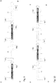
- FIG. 1 shows a schematic diagram of a terahertz mixer including a single frequency conversion unit according to an exemplary embodiment of the present disclosure.
- FIG. 2 shows a schematic diagram of a terahertz mixer including a plurality of frequency conversion units according to another exemplary embodiment of the present disclosure.
- the frequency conversion unit of the terahertz mixer includes a microstrip line 107 and a channel structure.
- the microstrip line 107 is located in the metal cavity.
- the channel structure includes a radio frequency signal input channel 101, a local oscillator signal input channel 102 and a signal output channel, which pass through the metal housing and are coupled to the microstrip line 107 respectively.
- a part of the microstrip line 107 respectively extends to the metal cavity where the radio frequency signal input channel 101 and the local oscillator signal input channel 102 are located, so as to form an antenna 104 for receiving radio frequency input signals and local oscillator input signals.
- Other composition parts and dimension parameters of the mixer may refer to the prior art, or other documents or patents.
- the radio frequency signal input channel 101 and the local oscillator signal input channel 102 of the mixer according to the present disclosure are respectively formed in the box body (or cover) defining the metal cavity and are parallel to the plane where the microstrip line 107 is located, and the signal output channel (which is an intermediate frequency signal output channel in this embodiment) is perpendicular to the plane where the microstrip line 107 is located and is led out from the cover or box body through an SMA connector 112.
- the terahertz mixer changes, by using the SMA connector, a direction along which the intermediate frequency signal of the mixer is led out, from the direction parallel to the plane where the microstrip line 107 is located to the direction perpendicular to the plane where the microstrip line 107 is located, thereby avoiding the problem of poor integration due to the presence of the radio frequency signal input channel, the local oscillator signal input channel and the signal output channel in the same plane. Moreover, it reduces the complexity and processing cost of multi-channel integration while ensuring the basic high-frequency characteristics of the mixer, which improves the flexibility of the mixer integration mode, and provides favorable conditions for further system integration.
- the SMA connector 112 is a wall-through structure and has a metal pin pointing outwards perpendicular to the principle plane.
- One end of the SMA connector 112 is level with the microstrip line 107 and connected to the intermediate frequency signal output port 103 of the microstrip line 107 through gold wire bonding, so as to realize a vertical extraction of the intermediate frequency signal.
- the SMA connector 112 may also adopt other connectors, such as a 2.92 mm connector.
- FIG. 3 shows a schematic diagram of a terahertz mixer including a single frequency conversion unit according to yet another exemplary embodiment of the present disclosure.
- FIG. 4 shows a schematic diagram of a terahertz mixer including a plurality of frequency conversion units according to yet another exemplary embodiment of the present disclosure.
- FIG. 5 shows a schematic diagram of a glass insulator according to an exemplary embodiment of the present disclosure.
- the signal output channel is led out vertically through a glass insulator.
- the glass insulator includes a metal pin 212 and a first columnar portion 213 sheathed on the middle of the metal pin 212.
- the metal pin 212 points outwards perpendicular to the principle plane, with a first end being level with the microstrip line 107 and connected to the intermediate frequency signal output port 103 of the microstrip line 107 through gold wire bonding.
- the first columnar part 213 is made of insulating glass medium.
- a metal layer 214 is provided on an outer surface of the first columnar part 213.
- the first columnar part 213 is connected to the cover or box body defining the metal housing, for example, located in a hole formed in the cover or box body.
- a second end of the metal pin 212 of the glass insulator which is opposite to the first end, is connected with an SMA connector so as to be connected to an external component.
- FIG. 6 shows a schematic diagram of a terahertz mixer including a single frequency conversion unit according to another exemplary embodiment of the present disclosure.
- FIG. 7 shows a schematic diagram of a terahertz mixer including a plurality of frequency conversion units according to yet another exemplary embodiment of the present disclosure.
- FIG. 8 shows a schematic diagram of a coaxial metal column structure according to an exemplary embodiment of the present disclosure.
- the signal output channel is led out vertically through the coaxial metal column.
- the coaxial metal column includes a metal pin 312 and a plurality of second columnar parts 313A, 313B, 313C, which are spaced apart from each other and sleeved on the metal pin 312 along the axial direction of the metal pin 312.
- One of the second columnar parts 313A, 313B, 313C (preferably the one far away from the intermediate frequency signal output port 103) is connected to the metal housing.
- the metal pin 312 points outwards perpendicular to the principle plane, with a first end being level with the microstrip line 107 and connected to the intermediate frequency signal output port 103 of the microstrip line through gold wire bonding.
- one of adjacent two of the second columnar parts 313A, 313B, 313C has a diameter difference from the other of the adjacent two of the second columnar parts 313A, 313B, 313C.
- the coaxial metal column adopts second columnar parts with different diameters to form effective filter characteristics, so that radio frequency signals and local oscillator signals may be filtered to ensure the output of intermediate frequency signals. Since the coaxial metal column integrates a low-pass filter, the overall length of the quartz microstrip line is shortened, thereby improving the integration of the multi-channel mixer.
- a second end of the metal pin 312 of the coaxial metal column which is opposite to the first end, is connected with an SMA connector so as to be connected to an external component.
- the intermediate frequency signal extraction direction may also be at an angle with respect to the plane where the microstrip line 107 is located, and the angle is not equal to zero.
- the radio frequency signal input channel 101 and the local oscillator signal input channel 102 of the frequency conversion unit are both introduced perpendicular to the length of the microstrip line 107 and directly coupled to the microstrip line.
- the radio frequency signal input channel 101 and the local oscillator signal input channel 102 of the frequency conversion unit may also be introduced in other directions.
- the radio frequency signal input channel 101 and the local oscillator signal input channel 102 of the frequency conversion unit are both introduced parallel to the length of the microstrip line 107 and coupled to the microstrip line through a 90° turn.
- the radio frequency signal input channel 101 and the local oscillator signal input channel 102 of the frequency conversion unit are introduced in opposite directions, so as to avoid interference of the radio frequency signal input channel 101, the local oscillator signal input channel 102 and their associated components in spatial position, and also shorten the overall length of the microstrip line 107, thereby further improving the integration of the mixer.
- the radio frequency signal input channel 101 and the local oscillator signal input channel 102 of the frequency conversion unit may also be introduced in the same direction.
- the introduction directions of the radio frequency signal input channel 101 and the local oscillator signal input channel 102 of the frequency conversion unit may not be parallel.
- the plurality of frequency conversion units are arranged in a row along the length of the microstrip line 107.
- the specific arrangements may be adjusted according to requirements.
- the radio frequency signal input channel 101 and the local oscillator signal input channel 102 of the frequency conversion unit are both introduced parallel to the length of the microstrip line 107 and coupled to the microstrip line 107 through a 90° turn
- the plurality of frequency conversion units may be arranged in a row along the direction perpendicular to the length of the microstrip line 107.
- other arrangements may also be adopted, and the specific arrangements may be adjusted according to requirements.
- the radio frequency signal input channels 101 of each row of frequency conversion units are parallel to each other and ports of the radio frequency signal input channels 101 are aligned with each other, and the local oscillator signal input channels 102 are parallel to each other and ports of the local oscillator signal input channels 102 are aligned with each other, so as to ensure that the signal reception of the multi-channel receiver and the input local oscillator signal are consistent.
- the operating process of the above-mentioned mixer includes the following.
- the terahertz signal that needs to be received passes through the radio frequency signal input channel 101.
- the terahertz signal is transmitted to the antenna 104 of the microstrip line 107.
- the local oscillator signal enters from the local oscillator signal input channel 102, passes through a microstrip transition structure 107 of a duplexer and a local oscillator low-pass filter 106, and then mixes with the radio frequency signal in a gallium arsenide Schottky diode 109.
- the radio frequency signal is mixed with second harmonic of the local oscillator.
- the differential intermediate frequency signal passes through an intermediate frequency filter 108 to the intermediate frequency signal output port 103, and then is transmitted to a load through the SMA connector or glass insulator or coaxial metal column.
- a ground line 105 connected to the metal cavity is led out from the microstrip line 107, which may be applied to the nearest metal cavity by conductive silver glue, or may be welded to the nearest metal cavity by gold wire bonding.
- FIG. 9 shows a schematic diagram of a distribution of a plurality of frequency conversion units of the terahertz mixer on the box body according to another exemplary embodiment of the present disclosure.
- FIG. 10 shows a schematic diagram of a distribution of a plurality of frequency conversion units of the terahertz mixer on the cover according to another exemplary embodiment of the present disclosure.
- the plurality of frequency conversion units are divided into two groups, which are respectively arranged in the box body (see FIG. 9 ) and the cover (see FIG. 10 ) and arranged in mirror symmetry.
- a microstrip line assembly position I of the frequency conversion unit in the cover corresponds to an air cavity position II on the microstrip line of the frequency conversion unit in the box body
- the air cavity position II on the microstrip line of the frequency conversion unit in the cover corresponds to the microstrip line assembly position I of the frequency conversion unit in the box body.
- the upper and lower adjacent channels have opposite intermediate frequency signal extraction directions, so as to be led out from the box body and the cover respectively, thereby reserving a large space for the SMA connector or glass insulator or coaxial metal column. If the SMA connector or glass insulator or coaxial metal column has the maximum outer diameter of a, then it is only needed to ensure that the spacing between channels is not less than a/2. If the spacing between channels needs to be further reduced, a custom small-size connector on the intermediate frequency output port may be employed.
- the signal output channels 103 of each row of frequency conversion units are parallel to each other, and two adjacent signal output channels are led out in opposite directions, so as to further reserve a large space for the SMA connector or glass insulator or coaxial metal column.
- A-A' to B'-B are marked at the corresponding positions of the box body and the cover to avoid incorrect buckling.
- the plurality of frequency conversion units may be one group all arranged on the box body or all arranged on the cover.
- the local oscillator signal input channels 102 of the plurality of frequency conversion units may be collected to a port through a (one to four, or one to eight) power divider, and then input signals through the local oscillator source, so as to realize the simultaneous operation of the mixer.
- the microstrip line 107 may be a quartz substrate-based microstrip line structure, or a sapphire-based microstrip line structure, or a common microstrip line structure, or a suspended microstrip line structure, or a monolithic integrated microstrip circuit of gallium arsenide (GaAs), or a monolithic integrated microstrip circuit of indium phosphide (InP).
- the material of the metal housing includes but is not limited to alloy metals such as aluminum or brass, and semiconductor materials based on silicon, or gallium arsenide, indium phosphide, and the like.
- the metal cavity defined by the metal housing may be a shielded cavity structure with a metal inner wall processed by a Micro-Electro-Mechanical System (MEMS) technology, or a shielded cavity structure with a metal inner wall processed by a micro-coaxial technology.
- MEMS Micro-Electro-Mechanical System
- the antenna 104 may be integrated and processed together with the radio frequency signal input channel 101.
- the size of the antenna 104 may be optimized according to the channel spacing to ensure the system's requirements for receiver parameters..
- the harmonic type of the mixer is not limited, and it may be a single-ended, single-balanced, double-balanced, triple-balanced, or I/Q passive mixer.
- the plurality of local oscillator signal input channels of the mixer may be collected to a port through a (one to four, or one to eight) power divider, and then input signals through the local oscillator source, so as to realize the simultaneous operation of the mixer.
- the terahertz mixer changes the direction along which the intermediate signal of the mixer is led out, from the direction parallel to the plane where the microstrip line 107 is located to the direction perpendicular to the plane where the microstrip line 107 is located, thereby avoiding the problem of poor integration due to the presence of the radio frequency signal input channel, the local oscillator signal input channel and the signal output channel in the same plane. Moreover, it reduces the complexity and processing cost of multi-channel integration while ensuring the basic high-frequency characteristics of the mixer, which improves the flexibility of the mixer integration mode, and provides favorable conditions for further system integration.
- the foregoing embodiments are all described by taking the mixer as an example, those skilled in the art should understand that in some other embodiments of the present disclosure, the device is also applicable to a frequency multiplier.
Landscapes
- Engineering & Computer Science (AREA)
- Power Engineering (AREA)
- Physics & Mathematics (AREA)
- Electromagnetism (AREA)
- Transceivers (AREA)
- Waveguides (AREA)
Abstract
Description
- The present disclosure relates to a field of communication technology, and in particular to a device for mixing or multiplying frequency.
- In recent years, terahertz wave technology, as an important research field, has attracted more and more attention at home and abroad. However, no matter which aspect and frequency band the terahertz wave is applied to, the reception of the terahertz wave is necessary. For the most commonly used receiver based on superheterodyne system, a mixer for frequency down conversion is a key component. In a solid-state terahertz radar and communications system, because a low-noise amplifier is difficult to implement, the mixer becomes the first stage of the receiving end, so the performance of the mixer is directly related to the performance of the entire receiver system. At the same time, since it is difficult to achieve a high-performance local oscillator in the same frequency band, sub-harmonic mixing technology is an effective way to solve this problem.
- With increased requirements of system performance, requirements of receiver indexes are also increasing. To improve integration or imaging resolution, multi-channel integration of the receiver is a key issue. Because the current terahertz mixers mainly use metal cavity materials such as copper or aluminum, which can achieve a good channel spacing, multi-channel at present is still spliced by independent single channels. However, due to limitations of machining requirements of the metal cavity, it is difficult to reduce the multi-channel spacing to improve the overall integration.
- The purpose of the present disclosure is to solve at least one aspect of the above-mentioned problems and defects existing in the prior art.
- According to an embodiment of the present disclosure, there is provided a device for mixing or multiplying frequency, including:
- a metal housing, including a box body and a cover buckled together to define a metal cavity;
- at least one frequency conversion unit, including:
- a microstrip line located in the metal cavity; and
- a channel structure, including a radio frequency signal input channel, a local oscillator signal input channel and a signal output channel, the radio frequency signal input channel, the local oscillator signal input channel and the signal output channel pass through the metal housing and are coupled to the microstrip line respectively, wherein the signal output channel is led out at an angle with respect to a plane where the microstrip line is located.
- According to the device of an exemplary embodiment of the present disclosure, the signal output channel is perpendicular to the plane where the microstrip line is located.
- According to the device of an exemplary embodiment of the present disclosure, the signal output channel is led out by using one of: an SMA connector; a glass insulator; or a coaxial metal column structure.
- According to the device of an exemplary embodiment of the present disclosure, the SMA connector is connected to a frequency output port of the microstrip line through gold wire bonding.
- According to the device of an exemplary embodiment of the present disclosure, the glass insulator is connected to the frequency output port of the microstrip line through gold wire bonding.
- According to the device of an exemplary embodiment of the present disclosure, the coaxial metal column structure includes a metal pin and a plurality of second columnar parts spaced apart from each other and sleeved on the metal pin along an axial direction of the metal pin, one of the second columnar parts is connected to the metal housing, and the metal pin is connected to a frequency output port of the microstrip line through gold wire bonding.
- According to the device of an exemplary embodiment of the present disclosure, one of adjacent two of the second columnar parts has a diameter different from the other of the adjacent two of the second columnar parts.
- According to the device of an exemplary embodiment of the present disclosure, the radio frequency signal input channel and the local oscillator signal input channel of the frequency conversion unit are both introduced into the microstrip line in a direction perpendicular to a length of the microstrip line and are coupled to the microstrip line.
- According to the device of an exemplary embodiment of the present disclosure, the radio frequency signal input channel and the local oscillator signal input channel of the frequency conversion unit are introduced in opposite directions.
- According to the device of an exemplary embodiment of the present disclosure, if the device includes a plurality of frequency conversion units, the plurality of frequency conversion units are divided into one group or two groups, and the frequency conversion units of each group are arranged in a row along the length of the microstrip line.
- According to the device of an exemplary embodiment of the present disclosure, the plurality of frequency conversion units are divided into two groups, the two groups of frequency conversion units are respectively arranged in the box body and the cover and are arranged in mirror symmetry.
- According to the device of an exemplary embodiment of the present disclosure, the radio frequency signal input channels of each row of the frequency conversion units are parallel to each other and ports of the radio frequency signal input channels of each row of the frequency conversion units are aligned with each other, and the local oscillator signal input channels of each row of the frequency conversion units are parallel to each other and ports of the local oscillator signal input channels of each row of the frequency conversion units are aligned with each other.
- According to the device of an exemplary embodiment of the present disclosure, the signal output channels of each row of the frequency conversion units are parallel to each other, and two adjacent signal output channels in each row of the frequency conversion units are led out in opposite directions.
- According to the device of an exemplary embodiment of the present disclosure, the device includes a plurality of frequency conversion units, the local oscillator signal input channels of the plurality of frequency conversion units are collected to one port through a power divider.
- In the device of mixing or multiplying frequency according to the above various embodiments of the present disclosure, the direction where the signal output channel is led out is changed from a direction parallel to the plane where the microstrip line is located to a direction at an angle to the plane where the microstrip line is located, which avoids the problem of poor integration due to the presence of the radio frequency signal input channel, the local oscillator signal input channel and the signal output channel in the same plane.
-
-
FIG. 1 shows a schematic diagram of a terahertz mixer including a single frequency conversion unit according to an exemplary embodiment of the present disclosure. -
FIG. 2 shows a schematic diagram of a terahertz mixer including a plurality of frequency conversion units according to another exemplary embodiment of the present disclosure. -
FIG. 3 shows a schematic diagram of a terahertz mixer including a single frequency conversion unit according to yet another exemplary embodiment of the present disclosure. -
FIG. 4 shows a schematic diagram of a terahertz mixer including a plurality of frequency conversion units according to yet another exemplary embodiment of the present disclosure. -
FIG. 5 shows a schematic diagram of a glass insulator according to an exemplary embodiment of the present disclosure. -
FIG. 6 shows a schematic diagram of a terahertz mixer including a single frequency conversion unit according to another exemplary embodiment of the present disclosure. -
FIG. 7 shows a schematic diagram of a terahertz mixer including a plurality of frequency conversion units according to yet another exemplary embodiment of the present disclosure. -
FIG. 8 shows a schematic diagram of a coaxial metal column structure according to an exemplary embodiment of the present disclosure. -
FIG. 9 shows a schematic diagram of a distribution of a plurality of frequency conversion units of the terahertz mixer on the box body according to another exemplary embodiment of the present disclosure. -
FIG. 10 shows a schematic diagram of a distribution of a plurality of frequency conversion units of the terahertz mixer on the cover according to another exemplary embodiment of the present disclosure. - Although the present disclosure will be fully described with reference to the drawings containing the preferred embodiments of the present disclosure, it should be understood that those skilled in the art may modify the invention described herein while obtaining the technical effects of the present disclosure. Therefore, it should be understood that the above description is a broad disclosure for those ordinary skilled in the art, and its content is not intended to limit the exemplary embodiments described in the present disclosure.
- In addition, in the following detailed description, for the convenience of explanation, many specific details are set forth to provide a comprehensive understanding of the embodiments of the present disclosure. Obviously, however, one or more embodiments may also be implemented without these specific details. In other cases, well-known structures and devices are shown in diagrammatic form to simplify the drawings.
- According to a general inventive concept of the present disclosure, there is provided a device of mixing or multiplying frequency, including: a metal housing including a box body and a cover buckled together to define a metal cavity; at least one frequency conversion unit including a microstrip line located in the metal cavity; and a channel structure including a radio frequency signal input channel, a local oscillator signal input channel and a signal output channel respectively passing through the metal housing and coupled to the microstrip line, wherein the signal output channel is led out at an angle with respect to a plane where the microstrip line is located.
- The terahertz mixer according to the present disclosure is a radio frequency transition microstrip line mixer, which mainly includes a metal housing and at least one frequency conversion unit located in the metal housing. The metal housing includes a box body and a cover buckled with the box body, for example, through a screw. A metal cavity may be defined in the metal housing when the box body and the cover are buckled together. In addition, the metal housing is further provided with a band port standard flange structure. In order to facilitate the connection of the cover and the box body, the terahertz mixer is further provided with alignment pins and the like.
-
FIG. 1 shows a schematic diagram of a terahertz mixer including a single frequency conversion unit according to an exemplary embodiment of the present disclosure.FIG. 2 shows a schematic diagram of a terahertz mixer including a plurality of frequency conversion units according to another exemplary embodiment of the present disclosure. - As shown in
FIGS. 1 and 2 , the frequency conversion unit of the terahertz mixer includes amicrostrip line 107 and a channel structure. Themicrostrip line 107 is located in the metal cavity. The channel structure includes a radio frequencysignal input channel 101, a local oscillatorsignal input channel 102 and a signal output channel, which pass through the metal housing and are coupled to themicrostrip line 107 respectively. A part of themicrostrip line 107 respectively extends to the metal cavity where the radio frequencysignal input channel 101 and the local oscillatorsignal input channel 102 are located, so as to form anantenna 104 for receiving radio frequency input signals and local oscillator input signals. Other composition parts and dimension parameters of the mixer may refer to the prior art, or other documents or patents. - The specific content of this solution will be described below in combination with more specific examples. It should be understood that the dimensions and proportions in the figures are only for illustration and have nothing to do with the actual structure.
- As shown in
FIGS. 1 and 2 , the radio frequencysignal input channel 101 and the local oscillatorsignal input channel 102 of the mixer according to the present disclosure are respectively formed in the box body (or cover) defining the metal cavity and are parallel to the plane where themicrostrip line 107 is located, and the signal output channel (which is an intermediate frequency signal output channel in this embodiment) is perpendicular to the plane where themicrostrip line 107 is located and is led out from the cover or box body through anSMA connector 112. The terahertz mixer changes, by using the SMA connector, a direction along which the intermediate frequency signal of the mixer is led out, from the direction parallel to the plane where themicrostrip line 107 is located to the direction perpendicular to the plane where themicrostrip line 107 is located, thereby avoiding the problem of poor integration due to the presence of the radio frequency signal input channel, the local oscillator signal input channel and the signal output channel in the same plane. Moreover, it reduces the complexity and processing cost of multi-channel integration while ensuring the basic high-frequency characteristics of the mixer, which improves the flexibility of the mixer integration mode, and provides favorable conditions for further system integration. - As shown in
FIGS. 1 and 2 , theSMA connector 112 is a wall-through structure and has a metal pin pointing outwards perpendicular to the principle plane. One end of theSMA connector 112 is level with themicrostrip line 107 and connected to the intermediate frequencysignal output port 103 of themicrostrip line 107 through gold wire bonding, so as to realize a vertical extraction of the intermediate frequency signal. Those skilled in the art should understand that theSMA connector 112 may also adopt other connectors, such as a 2.92 mm connector. -
FIG. 3 shows a schematic diagram of a terahertz mixer including a single frequency conversion unit according to yet another exemplary embodiment of the present disclosure.FIG. 4 shows a schematic diagram of a terahertz mixer including a plurality of frequency conversion units according to yet another exemplary embodiment of the present disclosure.FIG. 5 shows a schematic diagram of a glass insulator according to an exemplary embodiment of the present disclosure. - In some embodiments of the present disclosure, as shown in
FIGS. 3 and 4 , the signal output channel is led out vertically through a glass insulator. Specifically, as shown inFIG. 5 , the glass insulator includes ametal pin 212 and a firstcolumnar portion 213 sheathed on the middle of themetal pin 212. Themetal pin 212 points outwards perpendicular to the principle plane, with a first end being level with themicrostrip line 107 and connected to the intermediate frequencysignal output port 103 of themicrostrip line 107 through gold wire bonding. The firstcolumnar part 213 is made of insulating glass medium. Ametal layer 214 is provided on an outer surface of the firstcolumnar part 213. The firstcolumnar part 213 is connected to the cover or box body defining the metal housing, for example, located in a hole formed in the cover or box body. - In some embodiments of the present disclosure, a second end of the
metal pin 212 of the glass insulator, which is opposite to the first end, is connected with an SMA connector so as to be connected to an external component. -
FIG. 6 shows a schematic diagram of a terahertz mixer including a single frequency conversion unit according to another exemplary embodiment of the present disclosure.FIG. 7 shows a schematic diagram of a terahertz mixer including a plurality of frequency conversion units according to yet another exemplary embodiment of the present disclosure.FIG. 8 shows a schematic diagram of a coaxial metal column structure according to an exemplary embodiment of the present disclosure. - In some embodiments of the present disclosure, as shown in
FIGS. 6 and 7 , the signal output channel is led out vertically through the coaxial metal column. Specifically, as shown inFIG. 8 , the coaxial metal column includes ametal pin 312 and a plurality of secondcolumnar parts metal pin 312 along the axial direction of themetal pin 312. One of the secondcolumnar parts metal pin 312 points outwards perpendicular to the principle plane, with a first end being level with themicrostrip line 107 and connected to the intermediate frequencysignal output port 103 of the microstrip line through gold wire bonding. - In an exemplary embodiment of the present disclosure, as shown in
FIG. 8 , one of adjacent two of the secondcolumnar parts columnar parts - In some embodiments of the present disclosure, a second end of the
metal pin 312 of the coaxial metal column, which is opposite to the first end, is connected with an SMA connector so as to be connected to an external component. - It should be noted that although in the above-mentioned embodiment, through the SMA connector or the glass insulator or the coaxial metal column, the direction along which the intermediate frequency signal of the mixer is led out is changed from the direction parallel to the plane where the
microstrip line 107 is located to the direction perpendicular to the plane where themicrostrip line 107 is located, those skilled in the art should understand that in some other embodiments of the present disclosure, the intermediate frequency signal extraction direction may also be at an angle with respect to the plane where themicrostrip line 107 is located, and the angle is not equal to zero. - In some exemplary embodiments of the present disclosure, as shown in
FIGS. 1-4 ,6 and 7 , the radio frequencysignal input channel 101 and the local oscillatorsignal input channel 102 of the frequency conversion unit are both introduced perpendicular to the length of themicrostrip line 107 and directly coupled to the microstrip line. Those skilled in the art should understand that in some other embodiments of the present disclosure, the radio frequencysignal input channel 101 and the local oscillatorsignal input channel 102 of the frequency conversion unit may also be introduced in other directions. For example, the radio frequencysignal input channel 101 and the local oscillatorsignal input channel 102 of the frequency conversion unit are both introduced parallel to the length of themicrostrip line 107 and coupled to the microstrip line through a 90° turn. - In an exemplary embodiment of the present disclosure, as shown in
FIGS. 1-4 ,6 and 7 , the radio frequencysignal input channel 101 and the local oscillatorsignal input channel 102 of the frequency conversion unit are introduced in opposite directions, so as to avoid interference of the radio frequencysignal input channel 101, the local oscillatorsignal input channel 102 and their associated components in spatial position, and also shorten the overall length of themicrostrip line 107, thereby further improving the integration of the mixer. However, it should be noted that in some other embodiments of the present disclosure, the radio frequencysignal input channel 101 and the local oscillatorsignal input channel 102 of the frequency conversion unit may also be introduced in the same direction. In addition, in some other embodiments of the present disclosure, the introduction directions of the radio frequencysignal input channel 101 and the local oscillatorsignal input channel 102 of the frequency conversion unit may not be parallel. - In an exemplary embodiment, as shown in
FIGS. 2 ,4 and7 , in case that the device includes a plurality of frequency conversion units, the plurality of frequency conversion units are arranged in a row along the length of themicrostrip line 107. However, those skilled in the art should understand that in some other embodiments of the present disclosure, other arrangements may also be adopted, and the specific arrangements may be adjusted according to requirements. - In the case where the radio frequency
signal input channel 101 and the local oscillatorsignal input channel 102 of the frequency conversion unit are both introduced parallel to the length of themicrostrip line 107 and coupled to themicrostrip line 107 through a 90° turn, if the device includes a plurality of frequency conversion units, the plurality of frequency conversion units may be arranged in a row along the direction perpendicular to the length of themicrostrip line 107. However, those skilled in the art should understand that in some other embodiments of the present disclosure, other arrangements may also be adopted, and the specific arrangements may be adjusted according to requirements. - In an exemplary embodiment, as shown in
FIGS. 2 ,4 and7 , the radio frequencysignal input channels 101 of each row of frequency conversion units are parallel to each other and ports of the radio frequencysignal input channels 101 are aligned with each other, and the local oscillatorsignal input channels 102 are parallel to each other and ports of the local oscillatorsignal input channels 102 are aligned with each other, so as to ensure that the signal reception of the multi-channel receiver and the input local oscillator signal are consistent. - The operating process of the above-mentioned mixer includes the following. The terahertz signal that needs to be received passes through the radio frequency
signal input channel 101. In the waveguide-transition-microstrip line structure of the E-surface probe, the terahertz signal is transmitted to theantenna 104 of themicrostrip line 107. The local oscillator signal enters from the local oscillatorsignal input channel 102, passes through amicrostrip transition structure 107 of a duplexer and a local oscillator low-pass filter 106, and then mixes with the radio frequency signal in a galliumarsenide Schottky diode 109. The radio frequency signal is mixed with second harmonic of the local oscillator. The differential intermediate frequency signal passes through anintermediate frequency filter 108 to the intermediate frequencysignal output port 103, and then is transmitted to a load through the SMA connector or glass insulator or coaxial metal column. In order to avoid DC offset caused by the inconsistency of the pair ofSchottky diodes 109, aground line 105 connected to the metal cavity is led out from themicrostrip line 107, which may be applied to the nearest metal cavity by conductive silver glue, or may be welded to the nearest metal cavity by gold wire bonding. -
FIG. 9 shows a schematic diagram of a distribution of a plurality of frequency conversion units of the terahertz mixer on the box body according to another exemplary embodiment of the present disclosure.FIG. 10 shows a schematic diagram of a distribution of a plurality of frequency conversion units of the terahertz mixer on the cover according to another exemplary embodiment of the present disclosure. - In an exemplary embodiment, as shown in
FIGS. 9 and 10 , in case that the device includes a plurality of frequency conversion units, the plurality of frequency conversion units are divided into two groups, which are respectively arranged in the box body (seeFIG. 9 ) and the cover (seeFIG. 10 ) and arranged in mirror symmetry. Specifically, a microstrip line assembly position I of the frequency conversion unit in the cover corresponds to an air cavity position II on the microstrip line of the frequency conversion unit in the box body, and the air cavity position II on the microstrip line of the frequency conversion unit in the cover corresponds to the microstrip line assembly position I of the frequency conversion unit in the box body. In this way, the upper and lower adjacent channels have opposite intermediate frequency signal extraction directions, so as to be led out from the box body and the cover respectively, thereby reserving a large space for the SMA connector or glass insulator or coaxial metal column. If the SMA connector or glass insulator or coaxial metal column has the maximum outer diameter of a, then it is only needed to ensure that the spacing between channels is not less than a/2. If the spacing between channels needs to be further reduced, a custom small-size connector on the intermediate frequency output port may be employed. - In an exemplary embodiment, as shown in
FIG. 9 and FIG. 10 , thesignal output channels 103 of each row of frequency conversion units are parallel to each other, and two adjacent signal output channels are led out in opposite directions, so as to further reserve a large space for the SMA connector or glass insulator or coaxial metal column. - In an exemplary embodiment, as shown in
FIG. 9 and FIG. 10 , A-A' to B'-B are marked at the corresponding positions of the box body and the cover to avoid incorrect buckling. - It should be noted that if the device includes a plurality of frequency conversion units, the plurality of frequency conversion units may be one group all arranged on the box body or all arranged on the cover.
- In an exemplary embodiment, the local oscillator
signal input channels 102 of the plurality of frequency conversion units may be collected to a port through a (one to four, or one to eight) power divider, and then input signals through the local oscillator source, so as to realize the simultaneous operation of the mixer. - It should be noted that the
microstrip line 107 may be a quartz substrate-based microstrip line structure, or a sapphire-based microstrip line structure, or a common microstrip line structure, or a suspended microstrip line structure, or a monolithic integrated microstrip circuit of gallium arsenide (GaAs), or a monolithic integrated microstrip circuit of indium phosphide (InP). In addition, the material of the metal housing includes but is not limited to alloy metals such as aluminum or brass, and semiconductor materials based on silicon, or gallium arsenide, indium phosphide, and the like. The metal cavity defined by the metal housing may be a shielded cavity structure with a metal inner wall processed by a Micro-Electro-Mechanical System (MEMS) technology, or a shielded cavity structure with a metal inner wall processed by a micro-coaxial technology. - In addition, in an exemplary embodiment of the present disclosure, the
antenna 104 may be integrated and processed together with the radio frequencysignal input channel 101. The size of theantenna 104 may be optimized according to the channel spacing to ensure the system's requirements for receiver parameters.. - In addition, those skilled in the art should understand that the harmonic type of the mixer is not limited, and it may be a single-ended, single-balanced, double-balanced, triple-balanced, or I/Q passive mixer. The plurality of local oscillator signal input channels of the mixer may be collected to a port through a (one to four, or one to eight) power divider, and then input signals through the local oscillator source, so as to realize the simultaneous operation of the mixer.
- The terahertz mixer changes the direction along which the intermediate signal of the mixer is led out, from the direction parallel to the plane where the
microstrip line 107 is located to the direction perpendicular to the plane where themicrostrip line 107 is located, thereby avoiding the problem of poor integration due to the presence of the radio frequency signal input channel, the local oscillator signal input channel and the signal output channel in the same plane. Moreover, it reduces the complexity and processing cost of multi-channel integration while ensuring the basic high-frequency characteristics of the mixer, which improves the flexibility of the mixer integration mode, and provides favorable conditions for further system integration. In addition, although the foregoing embodiments are all described by taking the mixer as an example, those skilled in the art should understand that in some other embodiments of the present disclosure, the device is also applicable to a frequency multiplier. - Those skilled in the art may understand that the embodiments described above are exemplary, and those skilled in the art may make improvements. The structures described in the various embodiments may be combined freely without conflicts in structure or principle.
- After describing the preferred embodiments of the present disclosure in detail, those skilled in the art may clearly understand that various changes and modifications may be made without departing from the scope and spirit of the appended claims, and the present disclosure is not limited to the exemplary embodiments described in the present disclosure.
Claims (14)
- A device for mixing or multiplying frequency, comprising:a metal housing, comprising a box body and a cover buckled together to define a metal cavity;at least one frequency conversion unit, comprising:a microstrip line located in the metal cavity; anda channel structure comprising a radio frequency signal input channel, a local oscillator signal input channel and a signal output channel, the radio frequency signal input channel, the local oscillator signal input channel and the signal output channel pass through the metal housing and are coupled to the microstrip line respectively, wherein the signal output channel is led out at an angle with respect to a plane where the microstrip line is located.
- The device according to claim 1, wherein the signal output channel is perpendicular to the plane where the microstrip line is located.
- The device according to claim 1, wherein the signal output channel is led out by using one of an SMA connector, a glass insulator, or a coaxial metal column structure.
- The device according to claim 3, wherein the SMA connector is connected to a frequency output port of the microstrip line through gold wire bonding.
- The device according to claim 3, wherein the glass insulator is connected to a frequency output port of the microstrip line through gold wire bonding.
- The device according to claim 3, wherein the coaxial metal column structure includes a metal pin and a plurality of second columnar parts spaced apart from each other and sleeved on the metal pin along an axial direction of the metal pin, one of the second columnar parts is connected to the metal housing, and the metal pin is connected to a frequency output port of the microstrip line through gold wire bonding.
- The device according to claim 6, wherein one of adjacent two of the second columnar parts has a diameter different from the other of the adjacent two of the second columnar parts.
- The device according to any of claims 1 to 7, wherein the radio frequency signal input channel and the local oscillator signal input channel of the frequency conversion unit are both introduced into the microstrip line in a direction perpendicular to a length of the microstrip line and are coupled to the microstrip line.
- The device according to claim 8, wherein the radio frequency signal input channel and the local oscillator signal input channel of the frequency conversion unit are introduced in opposite directions.
- The device according to claim 9, wherein the device includes a plurality of frequency conversion units, the plurality of frequency conversion units are divided into one group or two groups, and the frequency conversion units of each group are arranged in a row along the length of the microstrip line.
- The device according to claim 10, wherein the plurality of frequency conversion units are divided into two groups, the two groups of frequency conversion units are respectively arranged in the box body and the cover and are arranged in mirror symmetry.
- The device according to claim 11, wherein the radio frequency signal input channels of each row of the frequency conversion units are parallel to each other and ports of the radio frequency signal input channels of each row of the frequency conversion units are aligned with each other, and the local oscillator signal input channels of each row of the frequency conversion units are parallel to each other and ports of the local oscillator signal input channels of each row of the frequency conversion units are aligned with each other.
- The device according to claim 12, wherein the signal output channels of each row of the frequency conversion units are parallel to each other, and two adjacent signal output channels in each row of the frequency conversion units are led out in opposite directions.
- The device according to any of claims 1 to 7, wherein the device includes a plurality of frequency conversion units, the local oscillator signal input channels of the plurality of frequency conversion units are collected to one port through a power divider.
Applications Claiming Priority (1)
| Application Number | Priority Date | Filing Date | Title |
|---|---|---|---|
| CN201911425658.6A CN113131871B (en) | 2019-12-31 | 2019-12-31 | A device that mixes or multiplies frequencies |
Publications (2)
| Publication Number | Publication Date |
|---|---|
| EP3846340A1 true EP3846340A1 (en) | 2021-07-07 |
| EP3846340B1 EP3846340B1 (en) | 2023-11-01 |
Family
ID=73789877
Family Applications (1)
| Application Number | Title | Priority Date | Filing Date |
|---|---|---|---|
| EP20212674.4A Active EP3846340B1 (en) | 2019-12-31 | 2020-12-09 | Device for mixing or multiplying frequency |
Country Status (3)
| Country | Link |
|---|---|
| EP (1) | EP3846340B1 (en) |
| CN (1) | CN113131871B (en) |
| BR (1) | BR102020025872A2 (en) |
Cited By (2)
| Publication number | Priority date | Publication date | Assignee | Title |
|---|---|---|---|---|
| CN114784475A (en) * | 2022-05-10 | 2022-07-22 | 电子科技大学 | Millimeter-wave waveguide-suspended microstrip probe transition structure with microstrip filtering branches |
| CN118969768A (en) * | 2024-07-31 | 2024-11-15 | 中国电子科技集团公司第十研究所 | RF connection structure of multi-layer SiP package based on glass substrate |
Citations (3)
| Publication number | Priority date | Publication date | Assignee | Title |
|---|---|---|---|---|
| CN202888829U (en) * | 2012-08-15 | 2013-04-17 | 深圳市海鹏信电子股份有限公司 | Strip-line antenna-feed lightning protection device |
| CN109509952A (en) * | 2018-12-29 | 2019-03-22 | 同方威视技术股份有限公司 | Terahertz frequency mixer and its manufacturing method and electronic equipment including the frequency mixer |
| CN209133660U (en) * | 2018-12-29 | 2019-07-19 | 同方威视技术股份有限公司 | Terahertz mixer and electronic device including the same |
Family Cites Families (5)
| Publication number | Priority date | Publication date | Assignee | Title |
|---|---|---|---|---|
| US4276655A (en) * | 1979-10-29 | 1981-06-30 | Sperry Corporation | Integrated circuit planar high frequency mixer |
| US4641369A (en) * | 1984-11-29 | 1987-02-03 | Trw Inc. | Local oscillator and mixer assembly |
| FR2928066A1 (en) * | 2008-02-27 | 2009-08-28 | Thomson Licensing Sas | SYSTEM FOR INTERCONNECTING TWO SUBSTRATES COMPRISING EACH AT LEAST ONE TRANSMISSION LINE |
| CN103684269B (en) * | 2013-12-16 | 2017-02-08 | 中国电子科技集团公司第四十一研究所 | Broadband-tunable 1mm subharmonic mixer |
| CN206340652U (en) * | 2016-12-28 | 2017-07-18 | 成都雷电微力科技有限公司 | Radio frequency vertical transition structure comprising ceramic micro-strip |
-
2019
- 2019-12-31 CN CN201911425658.6A patent/CN113131871B/en active Active
-
2020
- 2020-12-09 EP EP20212674.4A patent/EP3846340B1/en active Active
- 2020-12-17 BR BR102020025872-9A patent/BR102020025872A2/en unknown
Patent Citations (3)
| Publication number | Priority date | Publication date | Assignee | Title |
|---|---|---|---|---|
| CN202888829U (en) * | 2012-08-15 | 2013-04-17 | 深圳市海鹏信电子股份有限公司 | Strip-line antenna-feed lightning protection device |
| CN109509952A (en) * | 2018-12-29 | 2019-03-22 | 同方威视技术股份有限公司 | Terahertz frequency mixer and its manufacturing method and electronic equipment including the frequency mixer |
| CN209133660U (en) * | 2018-12-29 | 2019-07-19 | 同方威视技术股份有限公司 | Terahertz mixer and electronic device including the same |
Cited By (2)
| Publication number | Priority date | Publication date | Assignee | Title |
|---|---|---|---|---|
| CN114784475A (en) * | 2022-05-10 | 2022-07-22 | 电子科技大学 | Millimeter-wave waveguide-suspended microstrip probe transition structure with microstrip filtering branches |
| CN118969768A (en) * | 2024-07-31 | 2024-11-15 | 中国电子科技集团公司第十研究所 | RF connection structure of multi-layer SiP package based on glass substrate |
Also Published As
| Publication number | Publication date |
|---|---|
| EP3846340B1 (en) | 2023-11-01 |
| CN113131871B (en) | 2025-01-24 |
| BR102020025872A2 (en) | 2021-07-13 |
| CN113131871A (en) | 2021-07-16 |
Similar Documents
| Publication | Publication Date | Title |
|---|---|---|
| EP3846284A1 (en) | Device for mixing or multiplying frequency | |
| US8868021B1 (en) | Ultra-broadband planar millimeter-wave mixer with multi-octave IF bandwidth | |
| CN107196608B (en) | Novel terahertz frequency band broadband monolithic integration subharmonic mixer | |
| CN107276540B (en) | Terahertz image frequency suppression mixing circuit | |
| CN104166124B (en) | A kind of multiband borne Millimeter Wave Collision Avoidance Radars receiver | |
| WO2020134331A1 (en) | Terahertz mixer and manufacturing method therefor, and electronic device comprising mixer | |
| US12267100B2 (en) | Hetero-integrated terahertz low-noise miniaturized image frequency rejection transceiver front-end | |
| EP3846340B1 (en) | Device for mixing or multiplying frequency | |
| CN109617621A (en) | Adjustable Terahertz minimizes multifunctional unit radio-frequency front-end | |
| CN104092473A (en) | 3mm Band Receiver and Its Application | |
| US4270224A (en) | Microwave down converter | |
| US11984636B2 (en) | Active waveguide transition having a probe and RF amplifier system and which is usable in a transmit/receive communication system | |
| KR100471049B1 (en) | non-radiative dielectric waveguide mixer using a ring hybrid coupler | |
| CN107395128A (en) | Terahertz frequency mixer | |
| CN113131869B (en) | A device that mixes or multiplies frequencies | |
| US10193639B2 (en) | Over the air measurement module | |
| CN213186048U (en) | W-band subharmonic mixer | |
| CN113131163A (en) | Arrangements for mixing or multiplying frequencies | |
| CN101185194A (en) | High frequency electromagnetic wave receiver and broadband waveguide mixer | |
| CN113890488A (en) | Millimeter wave broadband single-balance down converter and frequency conversion method | |
| CN113131106B (en) | Terahertz mixer and electronic component | |
| CN119787982B (en) | A terahertz power combining circuit | |
| Paudel et al. | A THz Perpendicular Mode Converter for Interconnections Between Rectangular Waveguides to Substrate Integrated Waveguides | |
| JPH02206903A (en) | harmonic mixer | |
| CN120110319A (en) | A terahertz IQ second harmonic mixer |
Legal Events
| Date | Code | Title | Description |
|---|---|---|---|
| STAA | Information on the status of an ep patent application or granted ep patent |
Free format text: STATUS: REQUEST FOR EXAMINATION WAS MADE |
|
| PUAI | Public reference made under article 153(3) epc to a published international application that has entered the european phase |
Free format text: ORIGINAL CODE: 0009012 |
|
| 17P | Request for examination filed |
Effective date: 20201209 |
|
| AK | Designated contracting states |
Kind code of ref document: A1 Designated state(s): AL AT BE BG CH CY CZ DE DK EE ES FI FR GB GR HR HU IE IS IT LI LT LU LV MC MK MT NL NO PL PT RO RS SE SI SK SM TR |
|
| STAA | Information on the status of an ep patent application or granted ep patent |
Free format text: STATUS: EXAMINATION IS IN PROGRESS |
|
| 17Q | First examination report despatched |
Effective date: 20220404 |
|
| GRAP | Despatch of communication of intention to grant a patent |
Free format text: ORIGINAL CODE: EPIDOSNIGR1 |
|
| STAA | Information on the status of an ep patent application or granted ep patent |
Free format text: STATUS: GRANT OF PATENT IS INTENDED |
|
| INTG | Intention to grant announced |
Effective date: 20230524 |
|
| GRAS | Grant fee paid |
Free format text: ORIGINAL CODE: EPIDOSNIGR3 |
|
| GRAA | (expected) grant |
Free format text: ORIGINAL CODE: 0009210 |
|
| STAA | Information on the status of an ep patent application or granted ep patent |
Free format text: STATUS: THE PATENT HAS BEEN GRANTED |
|
| AK | Designated contracting states |
Kind code of ref document: B1 Designated state(s): AL AT BE BG CH CY CZ DE DK EE ES FI FR GB GR HR HU IE IS IT LI LT LU LV MC MK MT NL NO PL PT RO RS SE SI SK SM TR |
|
| REG | Reference to a national code |
Ref country code: GB Ref legal event code: FG4D |
|
| REG | Reference to a national code |
Ref country code: CH Ref legal event code: EP |
|
| REG | Reference to a national code |
Ref country code: IE Ref legal event code: FG4D |
|
| REG | Reference to a national code |
Ref country code: DE Ref legal event code: R096 Ref document number: 602020020186 Country of ref document: DE |
|
| P01 | Opt-out of the competence of the unified patent court (upc) registered |
Effective date: 20231208 |
|
| REG | Reference to a national code |
Ref country code: LT Ref legal event code: MG9D |
|
| REG | Reference to a national code |
Ref country code: NL Ref legal event code: MP Effective date: 20231101 |
|
| PG25 | Lapsed in a contracting state [announced via postgrant information from national office to epo] |
Ref country code: GR Free format text: LAPSE BECAUSE OF FAILURE TO SUBMIT A TRANSLATION OF THE DESCRIPTION OR TO PAY THE FEE WITHIN THE PRESCRIBED TIME-LIMIT Effective date: 20240202 |
|
| PG25 | Lapsed in a contracting state [announced via postgrant information from national office to epo] |
Ref country code: IS Free format text: LAPSE BECAUSE OF FAILURE TO SUBMIT A TRANSLATION OF THE DESCRIPTION OR TO PAY THE FEE WITHIN THE PRESCRIBED TIME-LIMIT Effective date: 20240301 |
|
| PG25 | Lapsed in a contracting state [announced via postgrant information from national office to epo] |
Ref country code: LT Free format text: LAPSE BECAUSE OF FAILURE TO SUBMIT A TRANSLATION OF THE DESCRIPTION OR TO PAY THE FEE WITHIN THE PRESCRIBED TIME-LIMIT Effective date: 20231101 |
|
| REG | Reference to a national code |
Ref country code: AT Ref legal event code: MK05 Ref document number: 1628379 Country of ref document: AT Kind code of ref document: T Effective date: 20231101 |
|
| PG25 | Lapsed in a contracting state [announced via postgrant information from national office to epo] |
Ref country code: NL Free format text: LAPSE BECAUSE OF FAILURE TO SUBMIT A TRANSLATION OF THE DESCRIPTION OR TO PAY THE FEE WITHIN THE PRESCRIBED TIME-LIMIT Effective date: 20231101 |
|
| PG25 | Lapsed in a contracting state [announced via postgrant information from national office to epo] |
Ref country code: AT Free format text: LAPSE BECAUSE OF FAILURE TO SUBMIT A TRANSLATION OF THE DESCRIPTION OR TO PAY THE FEE WITHIN THE PRESCRIBED TIME-LIMIT Effective date: 20231101 |
|
| PG25 | Lapsed in a contracting state [announced via postgrant information from national office to epo] |
Ref country code: ES Free format text: LAPSE BECAUSE OF FAILURE TO SUBMIT A TRANSLATION OF THE DESCRIPTION OR TO PAY THE FEE WITHIN THE PRESCRIBED TIME-LIMIT Effective date: 20231101 |
|
| PG25 | Lapsed in a contracting state [announced via postgrant information from national office to epo] |
Ref country code: NL Free format text: LAPSE BECAUSE OF FAILURE TO SUBMIT A TRANSLATION OF THE DESCRIPTION OR TO PAY THE FEE WITHIN THE PRESCRIBED TIME-LIMIT Effective date: 20231101 Ref country code: LT Free format text: LAPSE BECAUSE OF FAILURE TO SUBMIT A TRANSLATION OF THE DESCRIPTION OR TO PAY THE FEE WITHIN THE PRESCRIBED TIME-LIMIT Effective date: 20231101 Ref country code: IS Free format text: LAPSE BECAUSE OF FAILURE TO SUBMIT A TRANSLATION OF THE DESCRIPTION OR TO PAY THE FEE WITHIN THE PRESCRIBED TIME-LIMIT Effective date: 20240301 Ref country code: GR Free format text: LAPSE BECAUSE OF FAILURE TO SUBMIT A TRANSLATION OF THE DESCRIPTION OR TO PAY THE FEE WITHIN THE PRESCRIBED TIME-LIMIT Effective date: 20240202 Ref country code: ES Free format text: LAPSE BECAUSE OF FAILURE TO SUBMIT A TRANSLATION OF THE DESCRIPTION OR TO PAY THE FEE WITHIN THE PRESCRIBED TIME-LIMIT Effective date: 20231101 Ref country code: BG Free format text: LAPSE BECAUSE OF FAILURE TO SUBMIT A TRANSLATION OF THE DESCRIPTION OR TO PAY THE FEE WITHIN THE PRESCRIBED TIME-LIMIT Effective date: 20240201 Ref country code: AT Free format text: LAPSE BECAUSE OF FAILURE TO SUBMIT A TRANSLATION OF THE DESCRIPTION OR TO PAY THE FEE WITHIN THE PRESCRIBED TIME-LIMIT Effective date: 20231101 Ref country code: PT Free format text: LAPSE BECAUSE OF FAILURE TO SUBMIT A TRANSLATION OF THE DESCRIPTION OR TO PAY THE FEE WITHIN THE PRESCRIBED TIME-LIMIT Effective date: 20240301 |
|
| PG25 | Lapsed in a contracting state [announced via postgrant information from national office to epo] |
Ref country code: SE Free format text: LAPSE BECAUSE OF FAILURE TO SUBMIT A TRANSLATION OF THE DESCRIPTION OR TO PAY THE FEE WITHIN THE PRESCRIBED TIME-LIMIT Effective date: 20231101 Ref country code: RS Free format text: LAPSE BECAUSE OF FAILURE TO SUBMIT A TRANSLATION OF THE DESCRIPTION OR TO PAY THE FEE WITHIN THE PRESCRIBED TIME-LIMIT Effective date: 20231101 Ref country code: PL Free format text: LAPSE BECAUSE OF FAILURE TO SUBMIT A TRANSLATION OF THE DESCRIPTION OR TO PAY THE FEE WITHIN THE PRESCRIBED TIME-LIMIT Effective date: 20231101 Ref country code: NO Free format text: LAPSE BECAUSE OF FAILURE TO SUBMIT A TRANSLATION OF THE DESCRIPTION OR TO PAY THE FEE WITHIN THE PRESCRIBED TIME-LIMIT Effective date: 20240201 Ref country code: LV Free format text: LAPSE BECAUSE OF FAILURE TO SUBMIT A TRANSLATION OF THE DESCRIPTION OR TO PAY THE FEE WITHIN THE PRESCRIBED TIME-LIMIT Effective date: 20231101 Ref country code: HR Free format text: LAPSE BECAUSE OF FAILURE TO SUBMIT A TRANSLATION OF THE DESCRIPTION OR TO PAY THE FEE WITHIN THE PRESCRIBED TIME-LIMIT Effective date: 20231101 |
|
| PG25 | Lapsed in a contracting state [announced via postgrant information from national office to epo] |
Ref country code: DK Free format text: LAPSE BECAUSE OF FAILURE TO SUBMIT A TRANSLATION OF THE DESCRIPTION OR TO PAY THE FEE WITHIN THE PRESCRIBED TIME-LIMIT Effective date: 20231101 |
|
| PG25 | Lapsed in a contracting state [announced via postgrant information from national office to epo] |
Ref country code: CZ Free format text: LAPSE BECAUSE OF FAILURE TO SUBMIT A TRANSLATION OF THE DESCRIPTION OR TO PAY THE FEE WITHIN THE PRESCRIBED TIME-LIMIT Effective date: 20231101 |
|
| PG25 | Lapsed in a contracting state [announced via postgrant information from national office to epo] |
Ref country code: SK Free format text: LAPSE BECAUSE OF FAILURE TO SUBMIT A TRANSLATION OF THE DESCRIPTION OR TO PAY THE FEE WITHIN THE PRESCRIBED TIME-LIMIT Effective date: 20231101 |
|
| PG25 | Lapsed in a contracting state [announced via postgrant information from national office to epo] |
Ref country code: SM Free format text: LAPSE BECAUSE OF FAILURE TO SUBMIT A TRANSLATION OF THE DESCRIPTION OR TO PAY THE FEE WITHIN THE PRESCRIBED TIME-LIMIT Effective date: 20231101 Ref country code: SK Free format text: LAPSE BECAUSE OF FAILURE TO SUBMIT A TRANSLATION OF THE DESCRIPTION OR TO PAY THE FEE WITHIN THE PRESCRIBED TIME-LIMIT Effective date: 20231101 Ref country code: IT Free format text: LAPSE BECAUSE OF FAILURE TO SUBMIT A TRANSLATION OF THE DESCRIPTION OR TO PAY THE FEE WITHIN THE PRESCRIBED TIME-LIMIT Effective date: 20231101 Ref country code: EE Free format text: LAPSE BECAUSE OF FAILURE TO SUBMIT A TRANSLATION OF THE DESCRIPTION OR TO PAY THE FEE WITHIN THE PRESCRIBED TIME-LIMIT Effective date: 20231101 Ref country code: DK Free format text: LAPSE BECAUSE OF FAILURE TO SUBMIT A TRANSLATION OF THE DESCRIPTION OR TO PAY THE FEE WITHIN THE PRESCRIBED TIME-LIMIT Effective date: 20231101 Ref country code: CZ Free format text: LAPSE BECAUSE OF FAILURE TO SUBMIT A TRANSLATION OF THE DESCRIPTION OR TO PAY THE FEE WITHIN THE PRESCRIBED TIME-LIMIT Effective date: 20231101 |
|
| REG | Reference to a national code |
Ref country code: CH Ref legal event code: PL |
|
| REG | Reference to a national code |
Ref country code: DE Ref legal event code: R097 Ref document number: 602020020186 Country of ref document: DE |
|
| PG25 | Lapsed in a contracting state [announced via postgrant information from national office to epo] |
Ref country code: LU Free format text: LAPSE BECAUSE OF NON-PAYMENT OF DUE FEES Effective date: 20231209 |
|
| PG25 | Lapsed in a contracting state [announced via postgrant information from national office to epo] |
Ref country code: MC Free format text: LAPSE BECAUSE OF FAILURE TO SUBMIT A TRANSLATION OF THE DESCRIPTION OR TO PAY THE FEE WITHIN THE PRESCRIBED TIME-LIMIT Effective date: 20231101 |
|
| REG | Reference to a national code |
Ref country code: BE Ref legal event code: MM Effective date: 20231231 |
|
| PG25 | Lapsed in a contracting state [announced via postgrant information from national office to epo] |
Ref country code: MC Free format text: LAPSE BECAUSE OF FAILURE TO SUBMIT A TRANSLATION OF THE DESCRIPTION OR TO PAY THE FEE WITHIN THE PRESCRIBED TIME-LIMIT Effective date: 20231101 Ref country code: LU Free format text: LAPSE BECAUSE OF NON-PAYMENT OF DUE FEES Effective date: 20231209 |
|
| PLBE | No opposition filed within time limit |
Free format text: ORIGINAL CODE: 0009261 |
|
| STAA | Information on the status of an ep patent application or granted ep patent |
Free format text: STATUS: NO OPPOSITION FILED WITHIN TIME LIMIT |
|
| 26N | No opposition filed |
Effective date: 20240802 |
|
| REG | Reference to a national code |
Ref country code: IE Ref legal event code: MM4A |
|
| PG25 | Lapsed in a contracting state [announced via postgrant information from national office to epo] |
Ref country code: IE Free format text: LAPSE BECAUSE OF NON-PAYMENT OF DUE FEES Effective date: 20231209 |
|
| PG25 | Lapsed in a contracting state [announced via postgrant information from national office to epo] |
Ref country code: BE Free format text: LAPSE BECAUSE OF NON-PAYMENT OF DUE FEES Effective date: 20231231 |
|
| PG25 | Lapsed in a contracting state [announced via postgrant information from national office to epo] |
Ref country code: FR Free format text: LAPSE BECAUSE OF NON-PAYMENT OF DUE FEES Effective date: 20240101 |
|
| PG25 | Lapsed in a contracting state [announced via postgrant information from national office to epo] |
Ref country code: CH Free format text: LAPSE BECAUSE OF NON-PAYMENT OF DUE FEES Effective date: 20231231 |
|
| PG25 | Lapsed in a contracting state [announced via postgrant information from national office to epo] |
Ref country code: SI Free format text: LAPSE BECAUSE OF FAILURE TO SUBMIT A TRANSLATION OF THE DESCRIPTION OR TO PAY THE FEE WITHIN THE PRESCRIBED TIME-LIMIT Effective date: 20231101 |
|
| PG25 | Lapsed in a contracting state [announced via postgrant information from national office to epo] |
Ref country code: SI Free format text: LAPSE BECAUSE OF FAILURE TO SUBMIT A TRANSLATION OF THE DESCRIPTION OR TO PAY THE FEE WITHIN THE PRESCRIBED TIME-LIMIT Effective date: 20231101 Ref country code: IE Free format text: LAPSE BECAUSE OF NON-PAYMENT OF DUE FEES Effective date: 20231209 Ref country code: FR Free format text: LAPSE BECAUSE OF NON-PAYMENT OF DUE FEES Effective date: 20240101 Ref country code: CH Free format text: LAPSE BECAUSE OF NON-PAYMENT OF DUE FEES Effective date: 20231231 Ref country code: BE Free format text: LAPSE BECAUSE OF NON-PAYMENT OF DUE FEES Effective date: 20231231 |
|
| PG25 | Lapsed in a contracting state [announced via postgrant information from national office to epo] |
Ref country code: RO Free format text: LAPSE BECAUSE OF FAILURE TO SUBMIT A TRANSLATION OF THE DESCRIPTION OR TO PAY THE FEE WITHIN THE PRESCRIBED TIME-LIMIT Effective date: 20231101 |
|
| PG25 | Lapsed in a contracting state [announced via postgrant information from national office to epo] |
Ref country code: FI Free format text: LAPSE BECAUSE OF FAILURE TO SUBMIT A TRANSLATION OF THE DESCRIPTION OR TO PAY THE FEE WITHIN THE PRESCRIBED TIME-LIMIT Effective date: 20231101 |
|
| PG25 | Lapsed in a contracting state [announced via postgrant information from national office to epo] |
Ref country code: CY Free format text: LAPSE BECAUSE OF FAILURE TO SUBMIT A TRANSLATION OF THE DESCRIPTION OR TO PAY THE FEE WITHIN THE PRESCRIBED TIME-LIMIT; INVALID AB INITIO Effective date: 20201209 |
|
| PG25 | Lapsed in a contracting state [announced via postgrant information from national office to epo] |
Ref country code: HU Free format text: LAPSE BECAUSE OF FAILURE TO SUBMIT A TRANSLATION OF THE DESCRIPTION OR TO PAY THE FEE WITHIN THE PRESCRIBED TIME-LIMIT; INVALID AB INITIO Effective date: 20201209 |
|
| PG25 | Lapsed in a contracting state [announced via postgrant information from national office to epo] |
Ref country code: TR Free format text: LAPSE BECAUSE OF FAILURE TO SUBMIT A TRANSLATION OF THE DESCRIPTION OR TO PAY THE FEE WITHIN THE PRESCRIBED TIME-LIMIT Effective date: 20231101 |
|
| PGFP | Annual fee paid to national office [announced via postgrant information from national office to epo] |
Ref country code: GB Payment date: 20251111 Year of fee payment: 6 |
|
| PGFP | Annual fee paid to national office [announced via postgrant information from national office to epo] |
Ref country code: DE Payment date: 20251222 Year of fee payment: 6 |