EP3846237B1 - Organisches elektroelement, anzeigetafel damit und anzeigevorrichtung damit - Google Patents
Organisches elektroelement, anzeigetafel damit und anzeigevorrichtung damit Download PDFInfo
- Publication number
- EP3846237B1 EP3846237B1 EP20213723.8A EP20213723A EP3846237B1 EP 3846237 B1 EP3846237 B1 EP 3846237B1 EP 20213723 A EP20213723 A EP 20213723A EP 3846237 B1 EP3846237 B1 EP 3846237B1
- Authority
- EP
- European Patent Office
- Prior art keywords
- group
- compound
- chemical formula
- layer
- electric element
- Prior art date
- Legal status (The legal status is an assumption and is not a legal conclusion. Google has not performed a legal analysis and makes no representation as to the accuracy of the status listed.)
- Active
Links
Images


Classifications
-
- H—ELECTRICITY
- H10—SEMICONDUCTOR DEVICES; ELECTRIC SOLID-STATE DEVICES NOT OTHERWISE PROVIDED FOR
- H10K—ORGANIC ELECTRIC SOLID-STATE DEVICES
- H10K85/00—Organic materials used in the body or electrodes of devices covered by this subclass
- H10K85/60—Organic compounds having low molecular weight
- H10K85/611—Charge transfer complexes
-
- H—ELECTRICITY
- H10—SEMICONDUCTOR DEVICES; ELECTRIC SOLID-STATE DEVICES NOT OTHERWISE PROVIDED FOR
- H10K—ORGANIC ELECTRIC SOLID-STATE DEVICES
- H10K50/00—Organic light-emitting devices
-
- H—ELECTRICITY
- H10—SEMICONDUCTOR DEVICES; ELECTRIC SOLID-STATE DEVICES NOT OTHERWISE PROVIDED FOR
- H10K—ORGANIC ELECTRIC SOLID-STATE DEVICES
- H10K50/00—Organic light-emitting devices
- H10K50/10—OLEDs or polymer light-emitting diodes [PLED]
- H10K50/11—OLEDs or polymer light-emitting diodes [PLED] characterised by the electroluminescent [EL] layers
- H10K50/12—OLEDs or polymer light-emitting diodes [PLED] characterised by the electroluminescent [EL] layers comprising dopants
-
- H—ELECTRICITY
- H10—SEMICONDUCTOR DEVICES; ELECTRIC SOLID-STATE DEVICES NOT OTHERWISE PROVIDED FOR
- H10K—ORGANIC ELECTRIC SOLID-STATE DEVICES
- H10K50/00—Organic light-emitting devices
- H10K50/10—OLEDs or polymer light-emitting diodes [PLED]
- H10K50/11—OLEDs or polymer light-emitting diodes [PLED] characterised by the electroluminescent [EL] layers
- H10K50/125—OLEDs or polymer light-emitting diodes [PLED] characterised by the electroluminescent [EL] layers specially adapted for multicolour light emission, e.g. for emitting white light
- H10K50/13—OLEDs or polymer light-emitting diodes [PLED] characterised by the electroluminescent [EL] layers specially adapted for multicolour light emission, e.g. for emitting white light comprising stacked EL layers within one EL unit
-
- H—ELECTRICITY
- H10—SEMICONDUCTOR DEVICES; ELECTRIC SOLID-STATE DEVICES NOT OTHERWISE PROVIDED FOR
- H10K—ORGANIC ELECTRIC SOLID-STATE DEVICES
- H10K50/00—Organic light-emitting devices
- H10K50/10—OLEDs or polymer light-emitting diodes [PLED]
- H10K50/14—Carrier transporting layers
-
- H—ELECTRICITY
- H10—SEMICONDUCTOR DEVICES; ELECTRIC SOLID-STATE DEVICES NOT OTHERWISE PROVIDED FOR
- H10K—ORGANIC ELECTRIC SOLID-STATE DEVICES
- H10K50/00—Organic light-emitting devices
- H10K50/10—OLEDs or polymer light-emitting diodes [PLED]
- H10K50/17—Carrier injection layers
-
- H—ELECTRICITY
- H10—SEMICONDUCTOR DEVICES; ELECTRIC SOLID-STATE DEVICES NOT OTHERWISE PROVIDED FOR
- H10K—ORGANIC ELECTRIC SOLID-STATE DEVICES
- H10K59/00—Integrated devices, or assemblies of multiple devices, comprising at least one organic light-emitting element covered by group H10K50/00
- H10K59/10—OLED displays
- H10K59/12—Active-matrix OLED [AMOLED] displays
-
- H—ELECTRICITY
- H10—SEMICONDUCTOR DEVICES; ELECTRIC SOLID-STATE DEVICES NOT OTHERWISE PROVIDED FOR
- H10K—ORGANIC ELECTRIC SOLID-STATE DEVICES
- H10K85/00—Organic materials used in the body or electrodes of devices covered by this subclass
- H10K85/60—Organic compounds having low molecular weight
- H10K85/615—Polycyclic condensed aromatic hydrocarbons, e.g. anthracene
-
- H—ELECTRICITY
- H10—SEMICONDUCTOR DEVICES; ELECTRIC SOLID-STATE DEVICES NOT OTHERWISE PROVIDED FOR
- H10K—ORGANIC ELECTRIC SOLID-STATE DEVICES
- H10K85/00—Organic materials used in the body or electrodes of devices covered by this subclass
- H10K85/60—Organic compounds having low molecular weight
- H10K85/615—Polycyclic condensed aromatic hydrocarbons, e.g. anthracene
- H10K85/622—Polycyclic condensed aromatic hydrocarbons, e.g. anthracene containing four rings, e.g. pyrene
-
- H—ELECTRICITY
- H10—SEMICONDUCTOR DEVICES; ELECTRIC SOLID-STATE DEVICES NOT OTHERWISE PROVIDED FOR
- H10K—ORGANIC ELECTRIC SOLID-STATE DEVICES
- H10K85/00—Organic materials used in the body or electrodes of devices covered by this subclass
- H10K85/60—Organic compounds having low molecular weight
- H10K85/615—Polycyclic condensed aromatic hydrocarbons, e.g. anthracene
- H10K85/624—Polycyclic condensed aromatic hydrocarbons, e.g. anthracene containing six or more rings
-
- H—ELECTRICITY
- H10—SEMICONDUCTOR DEVICES; ELECTRIC SOLID-STATE DEVICES NOT OTHERWISE PROVIDED FOR
- H10K—ORGANIC ELECTRIC SOLID-STATE DEVICES
- H10K85/00—Organic materials used in the body or electrodes of devices covered by this subclass
- H10K85/60—Organic compounds having low molecular weight
- H10K85/615—Polycyclic condensed aromatic hydrocarbons, e.g. anthracene
- H10K85/626—Polycyclic condensed aromatic hydrocarbons, e.g. anthracene containing more than one polycyclic condensed aromatic rings, e.g. bis-anthracene
-
- H—ELECTRICITY
- H10—SEMICONDUCTOR DEVICES; ELECTRIC SOLID-STATE DEVICES NOT OTHERWISE PROVIDED FOR
- H10K—ORGANIC ELECTRIC SOLID-STATE DEVICES
- H10K85/00—Organic materials used in the body or electrodes of devices covered by this subclass
- H10K85/60—Organic compounds having low molecular weight
- H10K85/631—Amine compounds having at least two aryl rest on at least one amine-nitrogen atom, e.g. triphenylamine
-
- H—ELECTRICITY
- H10—SEMICONDUCTOR DEVICES; ELECTRIC SOLID-STATE DEVICES NOT OTHERWISE PROVIDED FOR
- H10K—ORGANIC ELECTRIC SOLID-STATE DEVICES
- H10K85/00—Organic materials used in the body or electrodes of devices covered by this subclass
- H10K85/60—Organic compounds having low molecular weight
- H10K85/631—Amine compounds having at least two aryl rest on at least one amine-nitrogen atom, e.g. triphenylamine
- H10K85/633—Amine compounds having at least two aryl rest on at least one amine-nitrogen atom, e.g. triphenylamine comprising polycyclic condensed aromatic hydrocarbons as substituents on the nitrogen atom
-
- H—ELECTRICITY
- H10—SEMICONDUCTOR DEVICES; ELECTRIC SOLID-STATE DEVICES NOT OTHERWISE PROVIDED FOR
- H10K—ORGANIC ELECTRIC SOLID-STATE DEVICES
- H10K85/00—Organic materials used in the body or electrodes of devices covered by this subclass
- H10K85/60—Organic compounds having low molecular weight
- H10K85/649—Aromatic compounds comprising a hetero atom
- H10K85/654—Aromatic compounds comprising a hetero atom comprising only nitrogen as heteroatom
-
- H—ELECTRICITY
- H10—SEMICONDUCTOR DEVICES; ELECTRIC SOLID-STATE DEVICES NOT OTHERWISE PROVIDED FOR
- H10K—ORGANIC ELECTRIC SOLID-STATE DEVICES
- H10K85/00—Organic materials used in the body or electrodes of devices covered by this subclass
- H10K85/60—Organic compounds having low molecular weight
- H10K85/649—Aromatic compounds comprising a hetero atom
- H10K85/657—Polycyclic condensed heteroaromatic hydrocarbons
- H10K85/6572—Polycyclic condensed heteroaromatic hydrocarbons comprising only nitrogen in the heteroaromatic polycondensed ring system, e.g. phenanthroline or carbazole
-
- H—ELECTRICITY
- H10—SEMICONDUCTOR DEVICES; ELECTRIC SOLID-STATE DEVICES NOT OTHERWISE PROVIDED FOR
- H10K—ORGANIC ELECTRIC SOLID-STATE DEVICES
- H10K2101/00—Properties of the organic materials covered by group H10K85/00
- H10K2101/30—Highest occupied molecular orbital [HOMO], lowest unoccupied molecular orbital [LUMO] or Fermi energy values
-
- H—ELECTRICITY
- H10—SEMICONDUCTOR DEVICES; ELECTRIC SOLID-STATE DEVICES NOT OTHERWISE PROVIDED FOR
- H10K—ORGANIC ELECTRIC SOLID-STATE DEVICES
- H10K50/00—Organic light-emitting devices
- H10K50/10—OLEDs or polymer light-emitting diodes [PLED]
- H10K50/14—Carrier transporting layers
- H10K50/15—Hole transporting layers
-
- H—ELECTRICITY
- H10—SEMICONDUCTOR DEVICES; ELECTRIC SOLID-STATE DEVICES NOT OTHERWISE PROVIDED FOR
- H10K—ORGANIC ELECTRIC SOLID-STATE DEVICES
- H10K50/00—Organic light-emitting devices
- H10K50/10—OLEDs or polymer light-emitting diodes [PLED]
- H10K50/17—Carrier injection layers
- H10K50/171—Electron injection layers
-
- H—ELECTRICITY
- H10—SEMICONDUCTOR DEVICES; ELECTRIC SOLID-STATE DEVICES NOT OTHERWISE PROVIDED FOR
- H10K—ORGANIC ELECTRIC SOLID-STATE DEVICES
- H10K50/00—Organic light-emitting devices
- H10K50/10—OLEDs or polymer light-emitting diodes [PLED]
- H10K50/19—Tandem OLEDs
Definitions
- Embodiments of the present disclosure relate to an organic electric element, a display panel, and a display device including the organic electric element.
- an organic light emitting phenomenon refers to the phenomenon of converting electrical energy into light energy by means of an organic material.
- An organic electric element refers to an electric element using the organic light emitting phenomenon.
- An organic electric element using the organic light emitting phenomenon may be applied to a display device. Since the portable display device is driven by a battery, which is a limited power source, an organic electric element used in the portable display device requires excellent light emission efficiency. In addition, since the image should be displayed normally during use of the electronic device, a long life of the organic electric element may be also required.
- US 2019/207123 Al discloses an organic light emitting diode comprising at least two light emitting stacks interposed between an anode and a cathode and a charge generation layer interposed between the light emitting stacks, where the charge generation layer comprises an N-type charge generation layer and a P-type charge generation layer, the N-type charge generation layer and the P-type charge generation layer are stacked in such direction for the N-type charge generation layer to face the anode and for the P-type charge generation layer to face the cathode, the N-type charge generation layer comprises substituted fused heterocylic compounds (I).
- WO 2018/221871 Al discloses an organic light emitting device including a charge generation layer comprising a p-type charge injection layer, a p-type charge generation layer, or a layer which simultaneously injects and generates p-type charges, and the p-type charge injection layer, the p-type charge generation layer, or the layer which simultaneously injects and generates p-type charges has electric conductivity of 1 ⁇ 10 -6 S/cm or more.
- embodiments of the present disclosure are directed to an organic electric element, a display panel, and a display device including the organic electric element that substantially obviate one or more of the problems due to limitations and disadvantages of the related art.
- An aspect of the present disclosure is to provide an organic electric element having high efficiency or long life.
- Another aspect of the present disclosure is to provide a display panel having high efficiency or long life by including the above-described organic electric element.
- Another aspect of the present disclosure is to provide a display device having high efficiency or long life by including the above-described display panel.
- an organic electric element according to claim 1. Further embodiments are described in the dependent claims. According to aspect, an organic electric element comprises a first electrode, a second electrode and an organic layer.
- the organic layer is positioned between the first electrode and the second electrode.
- the organic layer comprises a first stack comprising a first light emitting layer, a second stack comprising a second light emitting layer, and a charge generating layer positioned between the first stack and the second stack.
- the charge generating layer comprises a first layer and a second layer.
- the first layer comprises a first compound and a second compound.
- the first compound is represented by one or more of the following chemical formula 1 and chemical formula 2.
- the second compound is selected from one or more of the compounds 1-63 of claim 1.
- the second layer comprises a third compound represented by the following chemical formula 4.
- a display panel comprises a subpixel comprising the organic electric element.
- a display device comprises the display panel and a driving circuit for driving the display panel.
- the organic electric element having high luminous efficiency and long life.
- a display panel including the organic electric element having a high luminous efficiency and long life and a display device comprising the same.
- first element is connected or coupled to
- contacts or overlaps etc. a second element
- a third element can also be “interposed” between the first and second elements, or the first and second elements can “be connected or coupled to", “contact or overlap”, etc. each other via a fourth element.
- the second element may be included in at least one of two or more elements that "are connected or coupled to", “contact or overlap”, etc. each other.
- halo or halogen as used herein refers to fluorine (F), bromine (Br), chlorine (Cl), or iodine (I) unless otherwise indicated.
- alkyl or “alkyl group” refers to a saturated aliphatic functional radical of 1 to 60 carbon atoms with a single bond therein, including a straight chain alkyl group, a branched chain alkyl group, a cycloalkyl (alicyclic) group, an alkyl-substituted cycloalkyl group, and a cycloalkyl-substituted alkyl group, unless otherwise indicated.
- haloalkyl group or halogenalkyl group, as used herein, means a halogen-substituted alkyl group unless otherwise specified.
- heteroalkyl group means that at least one of the carbon atoms constituting the alkyl group has been replaced with a heteroatom.
- alkenyl group and “alkynyl group”, refer to a straight or branched chain of 2 to 60 carbon atoms with a double and a triple bond therein, respectively, unless stated otherwise, but are not limited thereto.
- cycloalkyl refers to an alkyl forming a ring having 3 to 60 carbon atoms, without being limited thereto.
- alkoxyl group means an alkyl group of 1 to 60 carbon atoms having an oxygen radical attached thereto, but is not limited thereto.
- alkenoxyl group means an alkenyl group of 2 to 60 carbon atoms having an oxygen radical attached thereto, unless otherwise stated, but is not limited thereto.
- aryloxyl group or “aryloxy group” means an aryl group of 6 to 60 carbon atoms having an oxygen radical attached thereto unless otherwise specified, but is not limited thereto.
- aryl group and “arylene group” each refer to having 6 to 60 carbon atoms unless otherwise stated, but are not limited thereto.
- an aryl group or an arylene group means a single or multiple aromatic ring, including an aromatic ring which is formed as neighboring substituents participate in a bond or a reaction.
- the aryl group may be a phenyl group, a biphenyl group, a terphenyl group, a naphthyl group, an anthracenyl group, a fluorene group, a spirofluorene group, or a spirobifluorene group.
- aryl or "ar” means a radical substituted with an aryl group.
- an arylalkyl group is an alkyl group substituted with an aryl group and an arylalkenyl group is an alkenyl group substituted with an aryl group.
- the radical substituted with an aryl group has the number of carbon atoms described herein.
- an arylalkoxy group means an alkoxy group substituted with an aryl group
- an alkoxylcarbonyl group means a carbonyl group substituted with an alkoxyl group
- an arylcarbonylalkenyl group means an alkenyl group substituted with an arylcarbonyl group wherein the arylcarbonyl group is a carbonyl group substituted with an aryl group.
- heteroalkyl means an alkyl bearing one or more heteroatoms unless otherwise indicated.
- heteroaryl group and “heteroarylene group” refer respectively to an aryl group and an arylene group of 2 to 60 carbon atoms bearing one or more heteroatoms therein, unless otherwise specified, without being limited thereto. It may include at least one of a single ring and multiple rings, and may be formed by combining adjacent functional groups.
- heterocyclic group refers to at least one of heteroaliphatic rings and heteroaromatic rings of 2 to 60 carbon atoms bearing one or more heteroatoms as a ring member thereof, which may be mono- or multi-cyclic and may be formed as neighboring functional groups combine with each other.
- heteroatom refers to N, O, S, P, or Si unless otherwise stated.
- Heterocyclic groups may also include rings comprising SO2, in place of carbon atoms, as a ring member.
- a “heterocyclic group” includes the following compounds.
- aliphatic as used herein means an aliphatic hydrocarbon of 1 to 60 carbon atoms
- aliphatic ring means an aliphatic hydrocarbon ring of 3 to 60 carbon atoms.
- ring refers to an aliphatic ring of 3 to 60 carbon atoms, an aromatic ring of 6 to 60 carbon atoms, a hetero ring of 2 to 60 carbon atoms, or a fused ring consisting of a combination thereof whether or not it is saturated or unsaturated.
- hetero-compounds or hetero-radicals other than the aforementioned hetero-compounds include, but are not limited to, one or more heteroatoms.
- carbonyl as used herein is represented by -COR', wherein R' is hydrogen, an alkyl group of 1 to 20 carbon atoms, an aryl group of 6 to 30 carbon atoms, a cycloalkyl group of 3 to 30 carbon atoms, an alkenyl group of 2 to 20 carbon atoms, an alkynyl group of 2 to 20 carbon atoms, or a combination thereof.
- ether as used herein is represented by -R-O-R', wherein R and R' are each independently hydrogen, an alkyl group of 1 to 20 carbon atoms, an aryl group of 6 to 30 carbon atoms, a cycloalkyl group of 3 to 30 carbon atoms, an alkenyl group of 2 to 20 carbon atoms, an alkynyl group of 2 to 20 carbon atoms, or a combination thereof.
- substituted in the expression “substituted or unsubstituted” means having at least one substituent selected from the group consisting of, but not limited to, deuterium, halogen, an amino group, a nitrile group, a nitro group, a C1-C20 alkyl group, a C1-C20 alkoxyl group, a C1-C20 alkylamine group, a C1-C20 alkylthiophene group, a C6-C20 arylthiophene group, a C2-C20 alkenyl group, a C2-C20 alkynyl, a C3-C20 cycloalkyl group, a C6-C20 aryl group, a deuterium-substituted C6-C20 aryl group, a C8-C20 aryl alkenyl group, a silane group, a boron group, a germanium
- the formation of a ring by combining substituents with each other means that adjacent groups combine with each other to form a monocycle or single ring, a ring aggregated or a conjugated multi-cycle, and the monocycle, the ring aggregated and the formed conjugated multicycle may include the heterocycle including at least one heteroatom, and may include aromatic and non-aromatic rings.
- the organic electric element may mean a component(s) between an anode and a cathode, or an organic light emitting diode including the anode, the cathode and the component(s) positioned therebetween.
- the organic electric element may mean one of an organic electric device, the organic light emitting diode and a panel including the same, and an electronic device including the panel and a circuit.
- the electronic device includes a display device, a lighting device, a solar cell, a portable or mobile terminal (e.g., a smart phone, a tablet, a PDA, an electronic dictionary, a PMP, etc.), a navigation terminal, a game machine, various TVs, and various computers monitor and the like, but is not limited thereto, and may be any type of device as long as the component(s) are included.
- FIG. 1 is a system configuration diagram of a display device according to embodiments.
- the display device 100 in accordance with embodiments of the present disclosure includes a display panel 110 in which a plurality of data lines DL and a plurality of gate lines GL are arranged and a plurality of sub-pixels 111 defined by the plurality of data lines DL and the plurality of gate lines GL is arranged, a data driving circuit DDC (or a data driver) for driving the plurality of data lines DL, a gate driving circuit GDC (or a gate driver) for driving the plurality of gate lines GL, a controller D-CTR controlling the data driving circuit DDC and the gate driving circuit GDC, and the like.
- a data driving circuit DDC or a data driver
- GDC gate driving circuit
- controller D-CTR controlling the data driving circuit DDC and the gate driving circuit GDC
- the controller D-CTR controls operations of the data driving circuit DDC and the gate driving circuit GDC by supplying respective control signals (DCS, GCS) to the data driving circuit DDC and the gate driving circuit GDC.
- the controller D-CTR starts the scan of pixels according to timings processed in each frame, converts image data inputted from other devices or other image providing sources to be adapted to a data signal form used in the data driving circuit DDC and then outputs image data DATA resulted from the converting, and causes the data to be loaded into the pixels at a preconfigured time according to the scan.
- the controller D-CTR may be implemented as a separate component from the data driving circuit DDC or may be integrated with data driving circuit DDC so the controller D-CTR can be implemented as an integrated circuit.
- the data driving circuit DDC drives the plurality of data lines DL by providing data voltages corresponding to image data DATA received from the controller D-CTR to the data lines DL.
- the data driving circuit DDC is sometimes referred to as a source driving circuit or a source driver.
- the data driving circuit DDC may include at least one source driver integrated circuit SDIC to be implemented.
- Each source driver integrated circuit SDIC may include a shift register, a latch circuit, a digital to analog converter DAC, an output buffer, and/or the like.
- each source driver integrated circuit SDIC may further include one or more analog to digital converters ADC.
- the gate driving circuit GDC sequentially drives a plurality of gate lines GL by sequentially providing scan signals to the plurality of gate lines GL.
- the gate driving circuit GDC is sometimes referred to as a scan driving circuit or a scan driver.
- the gate driving circuit GDC may include at least one gate driver integrated circuit GDIC to be implemented.
- Each gate driver integrated circuit GDIC may include a shift register, a level shifter, and/or the like.
- Each gate driver integrated circuit GDIC may be connected to a bonding pad of the display panel 110 in a tape automated bonding (TAB) type or a chip on glass (COG) type, or be directly disposed on the display panel 110 as being implemented in a gate in panel (GIP) type.
- TAB tape automated bonding
- COG chip on glass
- GIP gate in panel
- the gate driver integrated circuit GDIC may be disposed to be integrated with the display panel 110.
- each gate driver integrated circuit GDIC may be implemented in a chip on film (COF) type in which the gate driver integrated circuit GDIC is mounted on a film connected with the display panel 110.
- COF chip on film
- the gate driving circuit GDC sequentially provides scan signals of an on-voltage or an off-voltage to the plurality of gate lines GL.
- the data driving circuit DDC converts image data DATA received from the controller D-CTR into analog data voltages and provides the obtained analog data voltages to the plurality of data lines DL.
- the data driving circuit DDC may be located on, but not limited to, only one side (e.g., an upper side or a lower side) of the display panel 110, or in some instances, be located on, but not limited to, two sides (e.g., the upper side and the lower side) of the display panel 110 according to driving schemes, panel design schemes, or the like.
- the gate driving circuit GDC may be located on, but not limited to, only one side (e.g., a left side or a right side) of the panel 110, or in some instances, be located on, but not limited to, two sides (e.g., the left side and the right side) of the display panel 110 according to driving schemes, panel design schemes, or the like.
- the display device 100 may be one of various types of display devices, such as, a liquid crystal display device, an organic light emitting display device, a plasma display device, or the like.
- each sub-pixel 111 arranged in the display panel 110 may include circuit components, such as an organic light emitting diode (OLED), which is a self-emissive element, a driving transistor for driving the organic light emitting diode OLED, and the like.
- OLED organic light emitting diode
- Types of circuit elements and the number of the circuit elements included in each subpixel 111 may be different depending on types of the panel (e.g., an LCD panel, an OLED panel, etc.), provided functions, design schemes/features, or the like.
- FIG. 2 is a view illustrating a subpixel circuit of a display panel according to embodiments.
- each subpixel 111 may include an organic light emitting diode OLED and a driving transistor DRT for driving the organic light emitting diode OLED as basic circuit components.
- each sub-pixel 111 may further include a first transistor T1 allowing a data voltage VDATA to be applied to a first node N1 corresponding to a gate node of the driving transistor DRT, and a storage capacitor C1 for remaining a data voltage VDATA corresponding to an image signal voltage or a voltage corresponding to this during one frame time.
- the organic light emitting diode OLED may include a first electrode 221 (an anode electrode or a cathode electrode), a light emitting layer 222, a second electrode 223 (the cathode electrode or the anode electrode), and the like.
- a low-level voltage EVSS may be applied to the second electrode 223 of the organic light emitting diode OLED.
- the driving transistor DRT causes the organic light emitting diode OLED to be driven by providing a driving current to the organic light emitting diode OLED.
- the driving transistor DRT includes a first node N1, a second node N2 and a third node N3.
- the first node N1 of the driving transistor DRT may be a node corresponding to the gate node thereof, and may be electrically connected to a source node or a drain node of the first transistor T1.
- the second node N2 of the driving transistor DRT may be electrically connected to the first electrode 221 of the organic light emitting diode OLED and may be a source node or a drain node.
- the third node N3 of the driving transistor DRT may be the drain node or the source node as a node to which a driving voltage EVDD is applied, and may be electrically connected to a driving voltage line DVL used to supply a driving voltage EVDD.
- the first transistor T1 may be electrically connected between a data line DL and the first node N1 of the driving transistor DRT and may be controlled by a scan signal SCAN that is provided through a gate line and applied to the gate node of the first transistor T1.
- the storage capacitor C1 may be electrically connected between the first node N1 and the second node N2 of the driving transistor DRT.
- the storage capacitor C1 is an external capacitor intentionally designed to be located outside of the driving transistor DRT, not an internal storage, such as a parasitic capacitor (e.g., a Cgs, a Cgd) that presents between the first node N1 and the second node N2 of the driving transistor DRT.
- a parasitic capacitor e.g., a Cgs, a Cgd
- FIG. 3 is a cross-sectional view of a display device according to the embodiments.
- an organic electric element 320 includes a first electrode 321 and a second electrode 323, an organic layer 322 positioned therebetween.
- the first electrode 321 may be an anode and the second electrode 323 may be a cathode. In the case of an inverted type, the first electrode 321 may be a cathode and the second electrode 323 may be an anode.
- the first electrode 321 may be a transparent electrode, and the second electrode 323 may be a reflective electrode.
- the first electrode 321 may be a reflective electrode, and the second electrode 323 may be a transparent electrode.
- the organic layer 322 may include a plurality of layers which is located between the first electrode 321 and the second electrode 323 and includes an organic material.
- the organic layer includes a first stack 324, a second stack 325, and a charge generating layer 326 positioned between the first stack 324 and the second stack 325.
- the organic electric element 320 may be a tandem organic electric element including a plurality of stacks each including a light emitting layer.
- the plurality of light emitting layers may be made of the same material as each other, or may be made of different materials from each other.
- the first stack 324 includes a first light emitting layer 324a.
- the first light emitting layer 324a may include, for example, a host material and a dopant.
- the first stack 324 may further include a first hole transport layer 324b and a first electron transport layer 324c.
- the first hole transport layer 324b may be positioned between the first light emitting layer 324a and one of the first electrode 321 and the second electrode 323 as an anode electrode.
- the first electron transport layer 324c may be positioned between the first light emitting layer 324a and one of the first electrode 321 and the second electrode 323 as a cathode electrode.
- the first hole transport layer 324b may be positioned on the first electrode 321
- the first light emitting layer 324a may be positioned on the first hole transport layer 324b
- the first electron transport layer 324c may be positioned on the first light emitting layer 324a.
- the second stack 325 includes a second light emitting layer 325a.
- the second light emitting layer 325a may include, for example, a host material and a dopant.
- the second stack 325 may further include a second hole transport layer 325b and a second electron transport layer 325c.
- the second hole transport layer 325b may be positioned between the second light emitting layer 325a and one of the first electrode 321 and the second electrode 323 as an anode electrode.
- the second electron transport layer 325c may be positioned between the second light emitting layer 325a and one of the first electrode 321 and the second electrode 323 as a cathode electrode.
- the second hole transport layer 325b may be positioned on the first electrode 321
- the second light emitting layer 325a may be positioned on the second hole transport layer 325b
- the second electron transport layer 325c may be positioned on the second light emitting layer 325a.
- first stack 324 and the second stack 325 are configured as described above, holes and electrons transmitted from the first electrode 321 and the second electrode 323 are recombined with each other in the first and second light emitting layers 324a and 325a so that light may be emitted from the first and second light emitting layers 324a and 325a by recombination of holes and electrons.
- the charge generating layer 326 is formed between a plurality of light emitting layers to smoothly distribute charges so that it may increase the current efficiency of the light emitting layers. Accordingly, the charge generating layer 326 is positioned between the first stack 324 including the first light emitting layer 324a and the second stack 325 including the second light emitting layer 325a.
- the charge generating layer 326 may include a p-type charge generating layer and an n-type charge generating layer in order to smoothly distribute charges.
- the first layer 326a may be a p-type charge generating layer and the second layer 326b may be an n-type charge generating layer.
- the p-type charge generating layer may be located on the cathode electrode side and the n-type charge generating layer may be located on the anode side.
- the first layer 326a may be positioned between the second layer 326b and the second electrode 323 which is a cathode electrode.
- FIG. 3 shows the tandem organic electric element including two stacks
- the embodiment is not limited to the tandem organic electric element including two stacks, and includes tandem organic electric element including two or more stacks.
- a charge generating layer may be additionally positioned between the additionally included stack and one of the adjacent first stack 324 and the second stack 325.
- the organic electric element 320 may include a hole injection layer 327.
- the hole injection layer 327 may be positioned between the first electrode 321 as an anode electrode and the first light emitting layer 324a.
- the hole injection layer 327 may be positioned between the first electrode 321 as an anode electrode and the first hole transport layer 324b.
- the organic electric element 320 may further include an electron injection layer.
- the electron injection layer may be positioned between the second electrode 323 as a cathode electrode, and the second electron transport layer 325c.
- each of the first stack 324 and the second stack 325 may further include one or more of a hole injection layer and an electron injection layer.
- the hole injection layer may be located between the light emitting layer and the anode electrode
- an electron injection layer may be located between the light emitting layer and the cathode electrode.
- the first layer 326a includes the first compound.
- the first hole transport layer 324b may include the first compound, and the second hole transport layer 325b may also include the first compound. Further, the hole injection layer may also include the first compound.
- the first compound included in each layer may be the same as each other or may be different from each other as long as the requirements for the first compound described later are met.
- the first compound is represented by one or more of the following chemical formula 1 and chemical formula 2.
- R 1 to R 6 which are same or different, are each independently one selected from the group consisting of hydrogen; deuterium; tritium; a halogen; a cyano group; a nitro group; a C 6 -C 60 aryl group; a fluorenyl group; a C 2 -C 60 hetero ring group containing at least one hetero atom from O, N, S, Si and P; a fused ring group of a C 3 -C 60 aliphatic ring and a C 6 -C 60 aromatic ring; a C 1 -C 50 alkyl group; a C 2 -C 20 alkenyl group; a C 2 -C 20 alkynyl group; a C 1 -C 30 alkoxy group; a C 6 -C 30 aryloxy group; a C 3 -C 60 alkylsilyl group; a C 18 -C 60 arylsilyl group; and a C 8 -C 60 alkylaryl
- R 1 to R 6 are the aryl groups, they may be each independently a C 6 -C 60 aryl group, a C 6 -C 30 aryl group or a C 6 -C 12 aryl group.
- a 1 to A 4 which may be the same or different, are each independently one selected from the group consisting of hydrogen; deuterium; tritium; a halogen; a cyano group; a nitro group; a C 6 -C 60 aryl group; a fluorenyl group; a C 2 -C 60 hetero ring group containing at least one hetero atom from O, N, S, Si and P; a fused ring group of a C 3 -C 60 aliphatic ring and a C 6 -C 60 aromatic ring; a C 1 -C 50 alkyl group; a C 2 -C 20 alkenyl group; a C 2 -C 20 alkynyl group; a C 1 -C 30 alkoxy group; a C 6 -C 30 aryloxy group; a C 3 -C 60 alkylsilyl group; a C 18 -C 60 arylsilyl group; and a C 8 -C 60 alkyl
- the aryl group, the fluorenyl group, the hetero ring group, the fused ring group, the alkyl group, the alkenyl group, the alkynyl group, the alkoxy group, the aryloxy group, the alkylsilyl group, the arylsilyl group and the alkylarylsilyl group may each be further substituted with at least one substituent selected from the group consisting of deuterium; a nitro group; a cyano group; a halogen; an amino group; a C 1 -C 20 alkoxyl group; a C 1 -C 20 alkyl group; a C 2 - C 20 alkenyl group; a C 2 -C 20 alkynyl group; a C 6 -C 20 aryl group; a C 6 -C 20 aryl group substituted with deuterium; a fluorenyl group; a
- the first layer includes one compound (A) represented by chemical formula 1 and one compound (B) represented by chemical formula 2, it means that all the two compounds (A, B) are included in the first compound.
- the first layer 326b includes a second compound.
- the second compound is selected from one or more of the compounds 1-63 of claim 1. In an embodiment not forming part of the claimed invention, the second compound is represented by the following chemical formula 3.
- R 1 and R 2 which may be the same or different, are each independently one selected from the group consisting of a C 6 -C 60 aryl group; a fluorenyl group; a C 2 -C 60 hetero ring group containing at least one hetero atom from O, N, S, Si and P; a fused ring group of a C 3 -C 60 aliphatic ring and a C 6 -C 60 aromatic ring; a C 1 -C 60 alkyl group.
- R 1 and R 2 are the aryl group, they may be each independently the C 6 -C 60 aryl group, the C 6 -C 30 aryl group or the C 6 -C 12 aryl group.
- L is one selected from the group consisting of a C 6 -C 60 arylene group; a fluorylene group; a C 2 -C 60 divalent hetero ring group containing at least one heteroatom from O, N, S, Si and P; a divalent fused ring group of a C 3 -C 60 aliphatic ring and a C 6 -C 60 aromatic ring.
- L is the aryl group, it may be each independently the C 6 -C 60 aryl group, the C 6 -C 30 aryl group or the C 6 -C 12 aryl group.
- the aryl group, the fluorenyl group, the hetero ring group, the fused ring group, the arylene group, the fluorylene group, the C 2 -C 60 divalent hetero ring group and a divalent fused ring group may each be further substituted with at least one substituent selected from the group consisting of deuterium; a nitro group; a cyano group; a halogen; an amino group; a C 1 -C 20 alkoxyl group; a C 1 -C 20 alkyl group; a C 2 - C 20 alkenyl group; a C 2 -C 20 alkynyl group; a C 6 -C 20 aryl group; a C 6 -C 20 aryl group substituted with deuterium; a fluorenyl group; a C 2 -C 20 hetero ring group; a C 3 -C 60 alkylsilyl group; a C 18
- the second layer 326b includes a third compound.
- the third compound may be represented by the following chemical formula 4.
- R 1 to R 6 which are same or different, are each independently one selected from the group consisting of hydrogen; deuterium; tritium; a halogen; a nitro group; a C 6 -C 60 aryl group; a fluorenyl group; a C 2 -C 60 hetero ring group containing at least one hetero atom from O, N, S, Si and P; a fused ring group of a C 3 -C 60 aliphatic ring and a C 6 -C 60 aromatic ring; a C 1 -C 50 alkyl group; a C 2 -C 20 alkenyl group; a C 2 -C 20 alkynyl group; a C 1 -C 30 alkoxy group; a C 6 -C 30 aryloxy group; a C 3 -C 60 alkylsilyl group; a C 18 -C 60 arylsilyl group; and a C 8 -C 60 alkylarylsilyl group, and one
- R 1 to R 6 are the aryl groups, they may be each independently a C 6 -C 60 aryl group, a C 6 -C 30 aryl group or a C 6 -C 12 aryl group.
- R 1 to R 6 are the hetero ring group containing at least one hetero atom from O, N, S, Si and P, they may be each independently the C 6 -C 60 hetero ring group, the C 6 -C 50 hetero ring group or the C 6 -C 40 hetero ring group.
- Ar 1 and Ar 2 which are same or different, are each independently one selected from the group consisting of hydrogen; deuterium; tritium; a halogen; a cyano group; a nitro group; a C 6 -C 60 aryl group; a fluorenyl group; a C 2 -C 60 hetero ring group containing at least one hetero atom from O, N, S, Si and P; a fused ring group of a C 3 -C 60 aliphatic ring and a C 6 -C 60 aromatic ring; a C 1 -C 50 alkyl group; a C 2 -C 20 alkenyl group; a C 2 -C 20 alkynyl group; a C 1 -C 30 alkoxy group; a C 6 -C 30 aryloxy group; a C 3 -C 60 alkylsilyl group; a C 18 -C 60 arylsilyl group; and a C 8 -C 60 alkylaryl
- Ar 1 to Ar 6 are the aryl groups, they may be each independently a C 6 -C 60 aryl group, a C 6 -C 50 aryl group or a C 6 -C 40 aryl group.
- Ar 1 to Ar 6 are the hetero ring group containing at least one hetero atom from O, N, S, Si and P, they may be each independently the C 6 -C 60 hetero ring group, the C 6 -C 50 hetero ring group or the C 6 -C 40 hetero ring group.
- L is one selected from the group consisting of a C 6 -C 60 arylene group; a fluorylene group; a C 2 -C 60 divalent hetero ring group containing at least one heteroatom from O, N, S, Si and P; a divalent fused ring group of a C 3 -C 60 aliphatic ring and a C 6 -C 60 aromatic ring.
- the aryl group, the fluorenyl group, the hetero ring group, the fused ring group, the alkyl group, the alkenyl group, the alkynyl group, the alkoxy group, the aryloxy group, the alkylsilyl group, the arylsilyl group, the alkylarylsilyl group, the arylene group, the fluorylene group, the divalent fused ring group, the divalent fused ring group may each be further substituted with at least one substituent selected from the group consisting of deuterium; a nitro group; a cyano group; a halogen; an amino group; a C 1 -C 20 alkoxyl group; a C 1 -C 20 alkyl group; a C 2 - C 20 alkenyl group; a C 2 -C 20 alkynyl group; a C 6 -C 20 aryl group;
- the organic electric element 320 includes the first layer 326a including the first compound and the second compound and the second layer 326b including the third compound, it can have high efficiency or long life.
- the first chemical compound is represented by one or more of the following chemical formula 5 and chemical formula 6.
- n and m are each independently an integer from 0 to 5.
- R 7 to R 8 which may be the same or different, are each independently one selected from the group consisting of deuterium; tritium; a halogen; a cyano group; a C 1 -C 50 alkyl group; and a C 1 -C 30 alkoxy group.
- R 7 and R 8 are alkoxy groups, they may be, for example, a C 1 -C 30 alkoxy group, a C 1 -C 20 alkoxy group or a C 1 -C 10 alkoxy group.
- the alkyl group and the alkoxy group may each be further substituted with at least one substituent selected from the group consisting of deuterium and a halogen.
- the first layer includes one compound (C) represented by chemical formula 5 and one compound (D) represented by chemical formula 6, it means that all the two compounds (C, D) are included in the first compound.
- the organic electric element 320 may have high efficiency or long life.
- the first chemical compound is represented by one or more of the following chemical formula 7 and formula 8.
- R 1 to R 6 which are same or different, are each independently one selected from the group consisting of hydrogen; deuterium; tritium; a halogen; a cyano group; a nitro group; a C 6 -C 60 aryl group; a fluorenyl group; a C 2 -C 60 hetero ring group containing at least one hetero atom from O, N, S, Si and P; a fused ring group of a C 3 -C 60 aliphatic ring and a C 6 -C 60 aromatic ring; a C 1 -C 50 alkyl group; a C 2 -C 20 alkenyl group; a C 2 -C 20 alkynyl group; a C 1 -C 30 alkoxy group; a C 6 -C 30 aryloxy group; a C 3 -C 60 alkylsilyl group; a C 18 -C 60 arylsilyl group; and a C 8 -C 60 alkylaryl
- R 1 to R 6 are the aryl groups, they may be each independently a C 6 -C 60 aryl group, a C 6 -C 30 aryl group or a C 6 -C 12 aryl group.
- the aryl group, the fluorenyl group, the hetero ring group, the fused ring group, the alkyl group, the alkenyl group, the alkynyl group, the alkoxy group, the aryloxy group, the alkylsilyl group, the arylsilyl group and the alkylarylsilyl group may each be further substituted with at least one substituent selected from the group consisting of deuterium; a nitro group; a cyano group; a halogen; an amino group; a C 1 -C 20 alkoxyl group; a C 1 -C 20 alkyl group; a C 2 - C 20 alkenyl group; a C 2 -C 20 alkynyl group; a C 6 -C 20 aryl group; a C 6 -C 20 aryl group substituted with deuterium; a fluorenyl group; a C 2 -C 20
- the first layer includes one compound (E) represented by chemical formula 7 and one compound (F) represented by chemical formula 8, it means that all the two compounds (E, F) are included in the first compound.
- the organic electric element 320 may have high efficiency or long life.
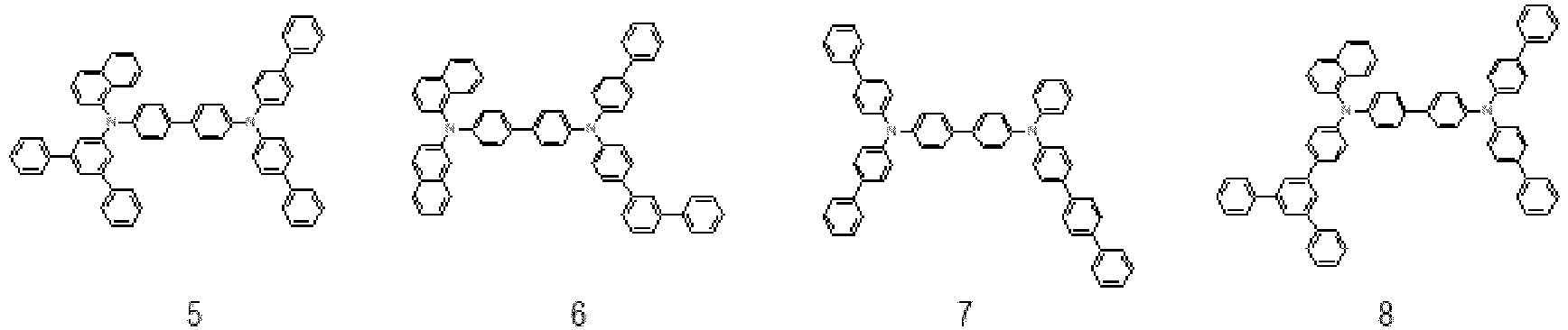
- the first chemical compound may be one or more of the following chemical compounds.
- the organic electric element 320 may have high efficiency or long life.
- the second chemical compound is one or more of the following chemical compounds.
- the organic electric element 320 may have high efficiency or long life.
- the third chemical compound is one or more of the following chemical compounds.
- the organic electric element 320 may have high efficiency or long life.
- the organic electric element 320 satisfies the following general formula 1.
- L 3 is the LUMO(Lowest Unoccupied Molecular Orbital) energy level of the third compound.
- L 1 is the LUMO energy level of the first compound.
- the upper limit of L 3 -L 1 defined in the general formula 1 may be 2.0 eV or less, or 1.8 eV or less.
- the organic electric element 320 includes a first layer including a first compound satisfying the general formula 1 so that it may have a high efficiency or long life.
- the organic electric element 320 satisfies the following general formula 2.
- L 1 is the LUMO(Lowest Unoccupied Molecular Orbital) energy level of the first compound.
- H 2 is the HOMO(Highest Occupied Molecular Orbital) energy level of the second compound.
- the upper limit of L 1 -H 2 defined in the general formula 2 may be 2.6 eV or less, or 2.4 eV or less.
- the organic electric element 320 includes the first and the second layers including the second and the third compounds satisfying the general formula 2 so that it may have a high efficiency or long life.
- the organic electric element 320 satisfies the following general formula 3. 0.32 eV ⁇ L 1 ⁇ H 2 ⁇ 0.6 eV
- L 1 is the LUMO(Lowest Unoccupied Molecular Orbital) energy level of the first compound.
- H 2 is the HOMO(Highest Occupied Molecular Orbital) energy level of the second compound.
- the lower limit of L 1 -H 2 defined in the general formula 3 may be 0.34 eV or more, or 0.38 eV or more.
- the upper limit of L 1 -H 2 defined in the general formula 3 may be 0.65 eV or less, or 0.50 eV or less.
- the organic electric element 320 includes a first layer including the first and the second compounds satisfying the general formula 3 so that it may have a high efficiency or long life.
- the first compound included in the first layer 326a may be a dopant, and the second compound may be a host compound. Since the first layer 326a includes the above-described first compound as the dopant and the above-described second compound as the host, the first layer 326a has excellent hole transport properties so that the organic electric element may have excellent efficiency and lifespan.
- the first compound may be doped at the ratio of 10% to 50% by weight into the first layer 326a.
- the first layer has excellent hole transport properties so that the organic electric element may have excellent efficiency and lifespan.
- the thickness of the first layer 326a is not particularly limited, but may be, for example, 50 ⁇ to 500 ⁇ .
- the thickness of the second layer 326b is not particularly limited, but may be, for example, 50 ⁇ to 500 ⁇ .
- the hole injection layer 327 may include a fourth compound and a fifth compound.
- the fourth compound may be represented by one or more of the chemical formulas 1 and 2.
- the fourth compound may be represented by one or more of Formula 5 and Formula 6, or may be represented by one or more of Formula 7 and Formula 8. That is, what has been described for the first compound can be applied to the fourth compound as it is.
- the specific fourth compound included in the organic electric element 320 according to the embodiments may be different from the first compound, or may be the same as each other.
- the fifth compound may be represented by the chemical formula 3 described above.
- the specific fifth compound included in the organic electric element 320 may be different from the second compound, or may be the same as each other.
- the organic electric element 320 includes a hole injection layer 327 including a fourth compound and a fifth compound, it may have high efficiency or long life.
- the fourth compound included in the hole injection layer 327 may be a dopant, and the fifth compound may be a host compound.
- the hole injection layer 327 includes the above-described fourth compound as the dopant, and the fifth compound as the host, so that the hole injection layer 327 has excellent hole injection characteristics so that the organic electric element may have excellent efficiency and lifespan.
- the fourth compound may be doped at a ratio of 10% to 50% by weight into the hole injection layer 327.
- the hole injection layer 327 has excellent hole injection characteristics, so that the organic electric element may have excellent efficiency and lifespan.
- the thickness of the hole injection layer 327 is not particularly limited, but may be, for example, 50 ⁇ to 500 ⁇ .
- FIG. 1 may depict a display panel 110.
- the display panel 110 includes a sub-pixel 111 including the above-described organic electric element 220.
- the organic electrical element 220 is the same as the organic electrical element 220 according to the above-described embodiments, a description thereof will be omitted.
- FIG. 1 may depict a display device 100.
- the display device 100 includes the above-described display panel 110 and a driving circuit for driving the above-described display panel 110.
- the display panel 110 is the same as the display panel 110 according to the above-described embodiments, so a description thereof will be omitted.
- a first hole transport layer was formed by thermal vacuum deposition of a hole transport material (NPD) of 100 nm.
- a second hole transport layer was formed by thermal vacuum deposition of a hole transport material (TCTA, Tris(4-carbazoyl-9-ylphenyl) amine) to a thickness of 100 nm.
- TCTA hole transport material
- ADN(9,10-di(naphtha-2-yl)anthracene) and 1,6-Bis (diphenylamine)pyrene were used as host and dopant materials, respectively, doped with 3%, and thermally vacuum-deposited to a thickness of 20 nm to form a first light emitting layer.
- a first electron transport layer was formed by thermal vacuum deposition of an electron transport material (TmPyPB, 1,3,5-Tri (m-pyridin-3-ylphenyl) benzene) to a thickness of 10 nm, and Bphen(Bathophenanthroline) as the third compound was used, and Li was doped with 2% to form a second layer (n-type charge generation layer) by thermal vacuum deposition to a thickness of 20 nm.
- an electron transport material TmPyPB, 1,3,5-Tri (m-pyridin-3-ylphenyl) benzene
- NPD N,N'-Di(1-naphthyl)-N,N'-diphenyl- (1,1'-biphenyl)-4,4'-diamine
- F4-TCNQ 2,3,5,6-tetrafluoro-tetracyanoquinodimethane
- NPD(N,N'-Di(1-naphthyl)-N,N'-diphenyl- (1,1'-biphenyl)-4,4'-diamine) as a hole transport material was vacuum-deposited to a thickness of 20nm and then CBP (4,4'-Bis (N-carbazolyl)-1,1'-biphenyl) is used as a host and Ir(ppy)3 (tris(2-phenylpyridine)Iridium (III) was doped with 10% as a dopant.
- Thermal vacuum deposition was performed to form a second light emitting layer of 20 nm.
- a second electron transport layer was formed by thermal vacuum deposition using Alq3 as an electron transport material, and then thermal vacuum deposition was performed using LiF as an electron injection material to form an electron injection layer.
- a cathode was formed by depositing Al to a thickness of 200 nm, thereby fabricating an organic electric element.
- the organic electric element was manufactured in the same manner as in the Comparative Example 1, except that the first compound, the second compound, the fourth compound, and the fifth compound were used in the types and ratios shown in Tables 1 and 2 below.
- Tables 3 and 4 show the performances of the manufactured organic electric elements.
- A04, A15 and A38 are chemical compounds described as being selectable as the first chemical compound
- 25, 34 and 60 are chemical compounds described as being selectable as the second chemical compounds
- E05 and E27 are chemical compounds described as being selectable as the third chemical compounds.
- F4-TCNQ is as follows.
- the organic electric element according to the embodiments includes the charge generating layer including the first layer including the first compound and the second compound according to claim 1 and the second layer including the third compound according to claim 1 so that it may have excellent efficiency or lifespan compared to the organic electric element of the Comparative Example.
- the organic electric element of the claimed invention including the first layer comprising the second compound selected from any of compounds 1-63 has better efficiency and longer life than the organic electric elements of Embodiments 1, 5 and 9.
- the organic electric element of the Embodiments comprising the second layer containing the third compound represented by the chemical formula 4 has better efficiency and longer life than the organic electric elements of Embodiments 1, 5 and 9.
- the organic electric element of the embodiments comprising the first layer comprising a second compound selected from any of compounds 1-63 and a second layer comprising a third compound represented by the chemical formula 4 has better efficiency and longer life than the organic electric elements of Embodiments 1, 5 and 9.
- a feature comprising the first compound represented by one or more of the chemical formulas 1 and 2 and the second compound selected from one or more of the compounds 1-63, and a feature comprising a third compound represented by the chemical formula 4 provide synergistic effects with each other to provide a more excellent organic electric element.
- the driving voltage, efficiency, and lifespan did not increase even when the doping ratio of the p-type doping material was increased, but in the case of the Embodiment, when the doping ratio of the first chemical compound that is the p-type doping material was increased, it can be seen that the organic electric element is improved in terms of the driving voltage, efficiency, or lifespan.
Landscapes
- Physics & Mathematics (AREA)
- Engineering & Computer Science (AREA)
- Spectroscopy & Molecular Physics (AREA)
- Chemical & Material Sciences (AREA)
- Materials Engineering (AREA)
- Optics & Photonics (AREA)
- Microelectronics & Electronic Packaging (AREA)
- Electroluminescent Light Sources (AREA)
Claims (13)
- Organisches elektrisches Element (320), aufweisend:eine erste Elektrode (321),eine zweite Elektrode (323) undeine zwischen der ersten Elektrode (321) und der zweiten Elektrode (323) angeordnete organische Schicht (322),wobei die organische Schicht (322) aufweist: einen ersten Stapel (324), der eine erste lichtemittierende Schicht (324a) aufweist, einen zweiten Stapel (325), der eine zweite lichtemittierende Schicht (325a) aufweist, und eine Ladungserzeugungsschicht (326), die zwischen dem ersten Stapel (324) und dem zweiten Stapel (325) angeordnet ist,die Ladungserzeugungsschicht (326) eine erste Schicht (326a) und eine zweite Schicht (326b) aufweist,die erste Schicht (326a) eine erste Verbindung, die durch eine oder mehrere der folgenden chemischen Formel 1 und chemischen Formel 2 dargestellt ist, und eine zweite Verbindung aufweist, unddie zweite Schicht (326b) eine dritte Verbindung aufweist, die durch die folgende chemische Formel 4 dargestellt ist:


 wobei in der chemischen Formel 1 und der chemischen Formel 2,R1 bis R6, die gleich oder verschieden sind, jeweils unabhängig voneinander eines sind, das ausgewählt ist aus der Gruppe bestehend aus Wasserstoff, Deuterium, Tritium, einem Halogen, einer Cyanogruppe, einer Nitrogruppe, einer C6-C60-Arylgruppe, einer Fluorenylgruppe, einer C2-C60-Heteroringgruppe, die mindestens ein Heteroatom aus O, N, S, Si und P enthält, einer kondensierten Ringgruppe aus einem aliphatischen C3-C60-Ring und einem aromatischen C6-C60-Ring, einer C1-C50-Alkylgruppe, einer C2-C20-Alkenylgruppe, einer C2-C20-Alkinylgruppe, einer C1-C30-Alkoxygruppe, einer C6-C30-Aryloxygruppe, einer C3-C60-Alkylsilylgruppe, einer C15-C60-Arylsilylgruppe und einer C8-C60-Alkylarylsilylgruppe, und eines oder mehrere von R1 bis R6 die Cyanogruppe ist,A1 bis A4, die gleich oder verschieden sein können, jeweils unabhängig voneinander eines sind, das ausgewählt ist aus der Gruppe bestehend aus Wasserstoff, Deuterium, Tritium, einem Halogen, einer Cyanogruppe, einer Nitrogruppe, einer C6-C60-Arylgruppe, einer Fluorenylgruppe, einer C2-C60-Heteroringgruppe, die mindestens ein Heteroatom aus O, N, S, Si und P enthält, einer kondensierten Ringgruppe aus einem aliphatischen C3-C60-Ring und einem aromatischen C6-C60-Ring, einer C1-C50-Alkylgruppe, einer C2-C20-Alkenylgruppe, einer C2-C20-Alkinylgruppe, einer C1-C30-Alkoxygruppe, einer C6-C30-Aryloxygruppe, einer C3-C60-Alkylsilylgruppe, einer C18-C60-Arylsilylgruppe und einer C8-C60-Alkylarylsilylgruppe,in R1 bis R6 und A1 bis A4 der chemischen Formel 1 und der chemischen Formel 2 die Arylgruppe, die Fluorenylgruppe, die Heteroringgruppe, die kondensierte Ringgruppe, die Alkylgruppe, die Alkenylgruppe, die Alkinylgruppe, die Alkoxygruppe, die Aryloxygruppe, die Alkylsilylgruppe, die Arylsilylgruppe und die Alkylarylsilylgruppe jeweils ferner mit mindestens einem Substituenten substituiert sein können, der ausgewählt ist aus der Gruppe bestehend aus Deuterium, einer Nitrogruppe, einer Cyanogruppe, einem Halogen, einer Aminogruppe, einer C1-C20-Alkoxylgruppe, einer C1-C20-Alkylgruppe, einer C2-C20-Alkenylgruppe, einer C2-C20-Alkinylgruppe, einer C6-C20-Arylgruppe, einer C6-C20-Arylgruppe, die mit Deuterium substituiert ist, einer Fluorenylgruppe, einer C2-C20-Heteroringgruppe, einer C3-C60-Alkylsilylgruppe, einer C18-C60-Arylsilylgruppe und einer C8-C60-Alkylarylsilylgruppe,wobei die zweite chemische Verbindung eine oder mehrere der folgenden Verbindungen ist:





 wobei in der chemischen Formel 4 R1 bis R6, die gleich oder verschieden sind, jeweils unabhängig voneinander eines sind, das ausgewählt ist aus der Gruppe bestehend aus Wasserstoff, Deuterium, Tritium, einem Halogen, einer Nitrogruppe, einer C6-C60-Arylgruppe, einer Fluorenylgruppe, einer C2-C60-Heteroringgruppe, die mindestens ein Heteroatom aus O, N, S, Si und P enthält, einer kondensierten Ringgruppe aus einem aliphatischen C3-C60-Ring und einem aromatischen C6-C60-Ring, einer C1-C50-Alkylgruppe, einer C2-C20-Alkenylgruppe, einer C2-C20-Alkinylgruppe, einer C1-C30-Alkoxygruppe, einer C6-C30-Aryloxygruppe, einer C3-C60-Alkylsilylgruppe, einer C18-C60-Arylsilylgruppe und einer C8-C60-Alkylarylsilylgruppe,Ar1 und Ar2, die gleich oder verschieden sind, jeweils unabhängig voneinander eines sind, das ausgewählt ist aus der Gruppe bestehend aus Wasserstoff, Deuterium, Tritium, einem Halogen, einer Cyanogruppe, einer Nitrogruppe, einer C6-C60-Arylgruppe, einer Fluorenylgruppe, einer C2-C60-Heteroringgruppe, die mindestens ein Heteroatom aus O, N, S, Si und P enthält, einer kondensierten Ringgruppe aus einem aliphatischen C3-C60-Ring und einem aromatischen C6-C60-Ring, einer C1-C50-Alkylgruppe, einer C2-C20-Alkenylgruppe, einer C2-C20-Alkinylgruppe, einer C1-C30-Alkoxygruppe, einer C6-C30-Aryloxygruppe, einer C3-C60-Alkylsilylgruppe, einer C18-C60-Arylsilylgruppe und einer C8-C60-Alkylarylsilylgruppe,L eines ist, das ausgewählt ist aus der Gruppe bestehend aus einer C6-C60-Arylengruppe, einer Fluorylengruppe, einer zweiwertigen C2-C60-Heteroringgruppe, die mindestens ein Heteroatom aus O, N, S, Si und P enthält, einer zweiwertigen kondensierten Ringgruppe aus einem aliphatischen C3-C60-Ring und einem aromatischen C6-C60-Ring, undin R1 bis R6, Ar1, Ar2 und L der chemischen Formel 4, die Arylgruppe, die Fluorenylgruppe, die Heteroringgruppe, die kondensierte Ringgruppe, die Alkylgruppe, die Alkenylgruppe, die Alkinylgruppe, die Alkoxygruppe, die Aryloxygruppe, die Alkylsilylgruppe, die Arylsilylgruppe, die Alkylarylsilylgruppe, die Arylengruppe, die Fluorylengruppe, die zweiwertige kondensierte Ringgruppe, die zweiwertige kondensierte Ringgruppe jeweils mit mindestens einem Substituenten weiter substituiert sein können, der ausgewählt ist aus der Gruppe bestehend aus Deuterium, einer Nitrogruppe, einer Cyanogruppe, einem Halogen, einer Aminogruppe, einer C1-C20-Alkoxylgruppe, einer C1-C20-Alkylgruppe, einer C2-C20-Alkenylgruppe, einer C2-C20-Alkinylgruppe, einer C6-C20-Arylgruppe, einer mit Deuterium substituierten C6-C20-Arylgruppe, einer Fluorenylgruppe, einer C2-C20-Heteroringgruppe, einer C3-C60-Alkylsilylgruppe, einer C18-C60-Arylsilylgruppe und einer C8-C60-Alkylarylsilylgruppe.
 - Organisches elektrisches Element (320) gemäß Anspruch 1, wobei die erste chemische Verbindung durch eine oder mehrere der folgenden chemischen Formel 5 und chemischen Formel 6 dargestellt ist:

 wobei in der chemischen Formel 5 und der chemischen Formel 6,n und m jeweils unabhängig voneinander eine ganze Zahl von 0 bis 5 sind,R7 bis R8, die gleich oder verschieden sein können, jeweils unabhängig eines sind, das ausgewählt ist aus der Gruppe bestehend aus Deuterium, Tritium, einem Halogen, einer Cyanogruppe, einer C1-C50-Alkylgruppe und einer C1-C30-Alkoxygruppe, undin R7 und R8 der chemischen Formel 5 und der chemischen Formel 6 die Alkylgruppe und die Alkoxygruppe jeweils weiter mit mindestens einem Substituenten substituiert sein können, der aus der Gruppe bestehend aus Deuterium und einem Halogen ausgewählt ist.
 - Organisches elektrisches Element (320) gemäß Anspruch 1, wobei die erste chemische Verbindung durch eine oder mehrere der folgenden chemischen Formel 7 und Formel 8 dargestellt ist:

 wobei in der chemischen Formel 7 und der chemischen Formel 8,R1 bis R6 gleich wie R1 bis R6 sind, die in den chemischen Formeln 1 und 2 definiert sind.
 - Organisches elektrisches Element (320) gemäß Anspruch 1, wobei die erste chemische Verbindung eine oder mehrere der folgenden chemischen Verbindungen ist:


- Organisches elektrisches Element (320) gemäß irgendeinem der Ansprüche 1 bis 4, wobei die dritte chemische Verbindung eine oder mehrere der folgenden chemischen Verbindungen ist:





- Organisches elektrisches Element (320) gemäß irgendeinem der Ansprüche 1 bis 5, wobei die erste Elektrode (321) eine Anodenelektrode ist, die zweite Elektrode (323) eine Kathodenelektrode ist und die erste Schicht (326a) zwischen der zweiten Schicht (326b) und der zweiten Elektrode (323) angeordnet ist.
- Organisches elektrisches Element (320) gemäß irgendeinem der Ansprüche 1 bis 6, ferner aufweisend eine Lochinjektionsschicht (327), die zwischen der ersten Elektrode (321) und der ersten lichtemittierenden Schicht (324a) angeordnet ist, wobei
die Lochinjektionsschicht (327) eine vierte Verbindung, die durch eine oder mehrere der chemischen Formel 1 und der chemischen Formel 2 dargestellt ist, und eine fünfte Verbindung, die durch die chemische Formel 3 dargestellt ist, aufweist. - Organisches elektrisches Element (320) gemäß Anspruch 7, wobei die vierte Verbindung die gleiche Verbindung wie die erste Verbindung ist und die fünfte Verbindung die gleiche Verbindung wie die zweite Verbindung ist.
- Organisches elektrisches Element (320) gemäß irgendeinem der Ansprüche 1 bis 8, wobei die folgende allgemeine Formel 1 erfüllt ist:
 L3 das Niedrigstes-Unbesetztes-Molekülorbital-, LUMO-, Energieniveau der dritten Verbindung ist, undL1 das LUMO-Energieniveau der ersten Verbindung ist.
 - Organisches elektrisches Element (320) gemäß irgendeinem der Ansprüche 1 bis 9, wobei die folgende allgemeine Formel 2 erfüllt ist:
 L3 das Niedrigstes-Unbesetztes-Molekülorbital-, LUMO-, Energieniveau der dritten Verbindung ist, undH1 das Höchstes-Besetztes-Molekülorbital-, HOMO-, Energieniveau der zweiten Verbindung ist.
 - Organisches elektrisches Element (320) gemäß irgendeinem der Ansprüche 1 bis 10, wobei die folgende allgemeine Formel 3 erfüllt ist:
 L1 das Niedrigstes-Unbesetztes-Molekülorbital-, LUMO-, Energieniveau der ersten Verbindung ist, undH2 das Höchstes-Besetztes-Molekülorbital-, HOMO-, Energieniveau der zweiten Verbindung ist.
 - Anzeigepanel (110), aufweisend ein Subpixel (111), welches das organische elektrische Element (320) gemäß irgendeinem der Ansprüche 1 bis 11 aufweist.
- Anzeigevorrichtung (100), aufweisend:das Anzeigepanel (111) gemäß Anspruch 12 undeine Treiberschaltung (GDC, DDC) zum Ansteuern des Anzeigepanels (111).
Applications Claiming Priority (1)
| Application Number | Priority Date | Filing Date | Title |
|---|---|---|---|
| KR1020190180017A KR102939742B1 (ko) | 2019-12-31 | 2019-12-31 | 유기전기소자, 이를 포함하는 표시패널 및 이를 포함하는 표시장치 |
Publications (2)
| Publication Number | Publication Date |
|---|---|
| EP3846237A1 EP3846237A1 (de) | 2021-07-07 |
| EP3846237B1 true EP3846237B1 (de) | 2025-04-02 |
Family
ID=73835389
Family Applications (1)
| Application Number | Title | Priority Date | Filing Date |
|---|---|---|---|
| EP20213723.8A Active EP3846237B1 (de) | 2019-12-31 | 2020-12-14 | Organisches elektroelement, anzeigetafel damit und anzeigevorrichtung damit |
Country Status (4)
| Country | Link |
|---|---|
| US (1) | US12364158B2 (de) |
| EP (1) | EP3846237B1 (de) |
| KR (1) | KR102939742B1 (de) |
| CN (1) | CN113130801B (de) |
Families Citing this family (1)
| Publication number | Priority date | Publication date | Assignee | Title |
|---|---|---|---|---|
| KR20220089235A (ko) * | 2020-12-21 | 2022-06-28 | 엘지디스플레이 주식회사 | 유기 화합물, 이를 포함하는 유기발광다이오드 및 유기발광장치 |
Family Cites Families (8)
| Publication number | Priority date | Publication date | Assignee | Title |
|---|---|---|---|---|
| KR20150102179A (ko) * | 2014-02-27 | 2015-09-07 | 삼성디스플레이 주식회사 | 표시 장치 및 이의 제조 방법 |
| US10096782B2 (en) * | 2014-08-01 | 2018-10-09 | Lg Display Co., Ltd. | Organic light emitting display device |
| KR102504145B1 (ko) | 2015-08-21 | 2023-02-27 | 엘지디스플레이 주식회사 | 유기전계발광소자 |
| KR102032599B1 (ko) * | 2015-10-06 | 2019-10-15 | 주식회사 엘지화학 | 아민 화합물 및 이를 포함하는 유기 발광 소자 |
| EP3176844B1 (de) * | 2015-12-03 | 2020-11-18 | LG Display Co., Ltd. | Organische lichtemittierende anzeigevorrichtung |
| KR102120520B1 (ko) * | 2016-09-23 | 2020-06-08 | 주식회사 엘지화학 | 아민계 화합물 및 이를 포함하는 유기 발광 소자 |
| KR102086890B1 (ko) * | 2017-05-31 | 2020-03-09 | 주식회사 엘지화학 | 유기 발광 소자 |
| KR102486441B1 (ko) * | 2017-12-28 | 2023-01-06 | 엘지디스플레이 주식회사 | 유기발광다이오드 |
-
2019
- 2019-12-31 KR KR1020190180017A patent/KR102939742B1/ko active Active
-
2020
- 2020-12-11 CN CN202011450053.5A patent/CN113130801B/zh active Active
- 2020-12-14 EP EP20213723.8A patent/EP3846237B1/de active Active
- 2020-12-29 US US17/136,559 patent/US12364158B2/en active Active
Also Published As
| Publication number | Publication date |
|---|---|
| CN113130801B (zh) | 2024-05-28 |
| US20210202845A1 (en) | 2021-07-01 |
| US12364158B2 (en) | 2025-07-15 |
| KR102939742B1 (ko) | 2026-03-16 |
| KR20210086221A (ko) | 2021-07-08 |
| CN113130801A (zh) | 2021-07-16 |
| EP3846237A1 (de) | 2021-07-07 |
Similar Documents
| Publication | Publication Date | Title |
|---|---|---|
| EP3846241A1 (de) | Organisches elektrisches element, anzeigetafel damit und anzeigevorrichtung damit | |
| US11997919B2 (en) | Organic electric element, display panel comprising the same and display device comprising the same | |
| EP3846239B1 (de) | Organisches elektrisches element, anzeigetafel damit und anzeigevorrichtung damit | |
| US20240040812A1 (en) | Organic electric element, display panel comprising the same and display device comprising the same | |
| EP3846242B1 (de) | Organisches elektrisches element, anzeigetafel damit und anzeigevorrichtung damit | |
| EP3846238A1 (de) | Organisches elektroelement, anzeigetafel damit und anzeigevorrichtung damit | |
| EP3846237B1 (de) | Organisches elektroelement, anzeigetafel damit und anzeigevorrichtung damit |
Legal Events
| Date | Code | Title | Description |
|---|---|---|---|
| STAA | Information on the status of an ep patent application or granted ep patent |
Free format text: STATUS: REQUEST FOR EXAMINATION WAS MADE |
|
| PUAI | Public reference made under article 153(3) epc to a published international application that has entered the european phase |
Free format text: ORIGINAL CODE: 0009012 |
|
| 17P | Request for examination filed |
Effective date: 20201214 |
|
| AK | Designated contracting states |
Kind code of ref document: A1 Designated state(s): AL AT BE BG CH CY CZ DE DK EE ES FI FR GB GR HR HU IE IS IT LI LT LU LV MC MK MT NL NO PL PT RO RS SE SI SK SM TR |
|
| RBV | Designated contracting states (corrected) |
Designated state(s): AL AT BE BG CH CY CZ DE DK EE ES FI FR GB GR HR HU IE IS IT LI LT LU LV MC MK MT NL NO PL PT RO RS SE SI SK SM TR |
|
| STAA | Information on the status of an ep patent application or granted ep patent |
Free format text: STATUS: EXAMINATION IS IN PROGRESS |
|
| 17Q | First examination report despatched |
Effective date: 20230403 |
|
| REG | Reference to a national code |
Ref country code: DE Free format text: PREVIOUS MAIN CLASS: H01L0051540000 Ref country code: DE Ref legal event code: R079 Ref document number: 602020048648 Country of ref document: DE Free format text: PREVIOUS MAIN CLASS: H01L0051540000 Ipc: H10K0085600000 |
|
| GRAP | Despatch of communication of intention to grant a patent |
Free format text: ORIGINAL CODE: EPIDOSNIGR1 |
|
| STAA | Information on the status of an ep patent application or granted ep patent |
Free format text: STATUS: GRANT OF PATENT IS INTENDED |
|
| RIC1 | Information provided on ipc code assigned before grant |
Ipc: H10K 50/19 20230101ALN20241010BHEP Ipc: H10K 85/60 20230101AFI20241010BHEP |
|
| RIC1 | Information provided on ipc code assigned before grant |
Ipc: H10K 50/19 20230101ALN20241015BHEP Ipc: H10K 85/60 20230101AFI20241015BHEP |
|
| INTG | Intention to grant announced |
Effective date: 20241024 |
|
| RIN1 | Information on inventor provided before grant (corrected) |
Inventor name: LEE, SUNGJAE Inventor name: LEE, YONGHAN Inventor name: KIM, DONGHEON Inventor name: YUN, JUN Inventor name: YOON, JOOYONG Inventor name: KIM, SHINHAN Inventor name: SEO, JEONGDAE Inventor name: YOO, SEONKEUN Inventor name: SHIN, JICHEOL |
|
| GRAS | Grant fee paid |
Free format text: ORIGINAL CODE: EPIDOSNIGR3 |
|
| GRAA | (expected) grant |
Free format text: ORIGINAL CODE: 0009210 |
|
| STAA | Information on the status of an ep patent application or granted ep patent |
Free format text: STATUS: THE PATENT HAS BEEN GRANTED |
|
| AK | Designated contracting states |
Kind code of ref document: B1 Designated state(s): AL AT BE BG CH CY CZ DE DK EE ES FI FR GB GR HR HU IE IS IT LI LT LU LV MC MK MT NL NO PL PT RO RS SE SI SK SM TR |
|
| REG | Reference to a national code |
Ref country code: GB Ref legal event code: FG4D |
|
| REG | Reference to a national code |
Ref country code: CH Ref legal event code: EP |
|
| REG | Reference to a national code |
Ref country code: IE Ref legal event code: FG4D |
|
| REG | Reference to a national code |
Ref country code: DE Ref legal event code: R096 Ref document number: 602020048648 Country of ref document: DE |
|
| REG | Reference to a national code |
Ref country code: NL Ref legal event code: MP Effective date: 20250402 |
|
| PG25 | Lapsed in a contracting state [announced via postgrant information from national office to epo] |
Ref country code: NL Free format text: LAPSE BECAUSE OF FAILURE TO SUBMIT A TRANSLATION OF THE DESCRIPTION OR TO PAY THE FEE WITHIN THE PRESCRIBED TIME-LIMIT Effective date: 20250402 |
|
| REG | Reference to a national code |
Ref country code: AT Ref legal event code: MK05 Ref document number: 1782621 Country of ref document: AT Kind code of ref document: T Effective date: 20250402 |
|
| PG25 | Lapsed in a contracting state [announced via postgrant information from national office to epo] |
Ref country code: FI Free format text: LAPSE BECAUSE OF FAILURE TO SUBMIT A TRANSLATION OF THE DESCRIPTION OR TO PAY THE FEE WITHIN THE PRESCRIBED TIME-LIMIT Effective date: 20250402 Ref country code: ES Free format text: LAPSE BECAUSE OF FAILURE TO SUBMIT A TRANSLATION OF THE DESCRIPTION OR TO PAY THE FEE WITHIN THE PRESCRIBED TIME-LIMIT Effective date: 20250402 Ref country code: PT Free format text: LAPSE BECAUSE OF FAILURE TO SUBMIT A TRANSLATION OF THE DESCRIPTION OR TO PAY THE FEE WITHIN THE PRESCRIBED TIME-LIMIT Effective date: 20250804 |
|
| REG | Reference to a national code |
Ref country code: LT Ref legal event code: MG9D |
|
| PG25 | Lapsed in a contracting state [announced via postgrant information from national office to epo] |
Ref country code: NO Free format text: LAPSE BECAUSE OF FAILURE TO SUBMIT A TRANSLATION OF THE DESCRIPTION OR TO PAY THE FEE WITHIN THE PRESCRIBED TIME-LIMIT Effective date: 20250702 Ref country code: GR Free format text: LAPSE BECAUSE OF FAILURE TO SUBMIT A TRANSLATION OF THE DESCRIPTION OR TO PAY THE FEE WITHIN THE PRESCRIBED TIME-LIMIT Effective date: 20250703 |
|
| PG25 | Lapsed in a contracting state [announced via postgrant information from national office to epo] |
Ref country code: PL Free format text: LAPSE BECAUSE OF FAILURE TO SUBMIT A TRANSLATION OF THE DESCRIPTION OR TO PAY THE FEE WITHIN THE PRESCRIBED TIME-LIMIT Effective date: 20250402 |
|
| PG25 | Lapsed in a contracting state [announced via postgrant information from national office to epo] |
Ref country code: BG Free format text: LAPSE BECAUSE OF FAILURE TO SUBMIT A TRANSLATION OF THE DESCRIPTION OR TO PAY THE FEE WITHIN THE PRESCRIBED TIME-LIMIT Effective date: 20250402 |
|
| PG25 | Lapsed in a contracting state [announced via postgrant information from national office to epo] |
Ref country code: HR Free format text: LAPSE BECAUSE OF FAILURE TO SUBMIT A TRANSLATION OF THE DESCRIPTION OR TO PAY THE FEE WITHIN THE PRESCRIBED TIME-LIMIT Effective date: 20250402 |
|
| PG25 | Lapsed in a contracting state [announced via postgrant information from national office to epo] |
Ref country code: AT Free format text: LAPSE BECAUSE OF FAILURE TO SUBMIT A TRANSLATION OF THE DESCRIPTION OR TO PAY THE FEE WITHIN THE PRESCRIBED TIME-LIMIT Effective date: 20250402 |
|
| PG25 | Lapsed in a contracting state [announced via postgrant information from national office to epo] |
Ref country code: RS Free format text: LAPSE BECAUSE OF FAILURE TO SUBMIT A TRANSLATION OF THE DESCRIPTION OR TO PAY THE FEE WITHIN THE PRESCRIBED TIME-LIMIT Effective date: 20250702 |
|
| PG25 | Lapsed in a contracting state [announced via postgrant information from national office to epo] |
Ref country code: IS Free format text: LAPSE BECAUSE OF FAILURE TO SUBMIT A TRANSLATION OF THE DESCRIPTION OR TO PAY THE FEE WITHIN THE PRESCRIBED TIME-LIMIT Effective date: 20250802 |
|
| PG25 | Lapsed in a contracting state [announced via postgrant information from national office to epo] |
Ref country code: LV Free format text: LAPSE BECAUSE OF FAILURE TO SUBMIT A TRANSLATION OF THE DESCRIPTION OR TO PAY THE FEE WITHIN THE PRESCRIBED TIME-LIMIT Effective date: 20250402 |
|
| REG | Reference to a national code |
Ref country code: DE Ref legal event code: R097 Ref document number: 602020048648 Country of ref document: DE |
|
| PGFP | Annual fee paid to national office [announced via postgrant information from national office to epo] |
Ref country code: DE Payment date: 20251020 Year of fee payment: 6 |
|
| PGFP | Annual fee paid to national office [announced via postgrant information from national office to epo] |
Ref country code: GB Payment date: 20251023 Year of fee payment: 6 |
|
| PG25 | Lapsed in a contracting state [announced via postgrant information from national office to epo] |
Ref country code: DK Free format text: LAPSE BECAUSE OF FAILURE TO SUBMIT A TRANSLATION OF THE DESCRIPTION OR TO PAY THE FEE WITHIN THE PRESCRIBED TIME-LIMIT Effective date: 20250402 Ref country code: SM Free format text: LAPSE BECAUSE OF FAILURE TO SUBMIT A TRANSLATION OF THE DESCRIPTION OR TO PAY THE FEE WITHIN THE PRESCRIBED TIME-LIMIT Effective date: 20250402 |
|
| PGFP | Annual fee paid to national office [announced via postgrant information from national office to epo] |
Ref country code: FR Payment date: 20251021 Year of fee payment: 6 |
|
| PG25 | Lapsed in a contracting state [announced via postgrant information from national office to epo] |
Ref country code: CZ Free format text: LAPSE BECAUSE OF FAILURE TO SUBMIT A TRANSLATION OF THE DESCRIPTION OR TO PAY THE FEE WITHIN THE PRESCRIBED TIME-LIMIT Effective date: 20250402 |
|
| PG25 | Lapsed in a contracting state [announced via postgrant information from national office to epo] |
Ref country code: EE Free format text: LAPSE BECAUSE OF FAILURE TO SUBMIT A TRANSLATION OF THE DESCRIPTION OR TO PAY THE FEE WITHIN THE PRESCRIBED TIME-LIMIT Effective date: 20250402 |
|
| PG25 | Lapsed in a contracting state [announced via postgrant information from national office to epo] |
Ref country code: SK Free format text: LAPSE BECAUSE OF FAILURE TO SUBMIT A TRANSLATION OF THE DESCRIPTION OR TO PAY THE FEE WITHIN THE PRESCRIBED TIME-LIMIT Effective date: 20250402 Ref country code: RO Free format text: LAPSE BECAUSE OF FAILURE TO SUBMIT A TRANSLATION OF THE DESCRIPTION OR TO PAY THE FEE WITHIN THE PRESCRIBED TIME-LIMIT Effective date: 20250402 |
|
| PG25 | Lapsed in a contracting state [announced via postgrant information from national office to epo] |
Ref country code: IT Free format text: LAPSE BECAUSE OF FAILURE TO SUBMIT A TRANSLATION OF THE DESCRIPTION OR TO PAY THE FEE WITHIN THE PRESCRIBED TIME-LIMIT Effective date: 20250402 |
|
| PLBE | No opposition filed within time limit |
Free format text: ORIGINAL CODE: 0009261 |
|
| STAA | Information on the status of an ep patent application or granted ep patent |
Free format text: STATUS: NO OPPOSITION FILED WITHIN TIME LIMIT |
|
| REG | Reference to a national code |
Ref country code: CH Ref legal event code: L10 Free format text: ST27 STATUS EVENT CODE: U-0-0-L10-L00 (AS PROVIDED BY THE NATIONAL OFFICE) Effective date: 20260211 |
|
| 26N | No opposition filed |
Effective date: 20260105 |