EP3845288A1 - Percolating filter - Google Patents
Percolating filter Download PDFInfo
- Publication number
- EP3845288A1 EP3845288A1 EP19908550.7A EP19908550A EP3845288A1 EP 3845288 A1 EP3845288 A1 EP 3845288A1 EP 19908550 A EP19908550 A EP 19908550A EP 3845288 A1 EP3845288 A1 EP 3845288A1
- Authority
- EP
- European Patent Office
- Prior art keywords
- base material
- surface layer
- filtration filter
- pdni
- intermediate layer
- Prior art date
- Legal status (The legal status is an assumption and is not a legal conclusion. Google has not performed a legal analysis and makes no representation as to the accuracy of the status listed.)
- Granted
Links
Images




Classifications
-
- B—PERFORMING OPERATIONS; TRANSPORTING
- B01—PHYSICAL OR CHEMICAL PROCESSES OR APPARATUS IN GENERAL
- B01D—SEPARATION
- B01D39/00—Filtering material for liquid or gaseous fluids
- B01D39/14—Other self-supporting filtering material ; Other filtering material
- B01D39/20—Other self-supporting filtering material ; Other filtering material of inorganic material, e.g. asbestos paper, metallic filtering material of non-woven wires
- B01D39/2027—Metallic material
-
- C—CHEMISTRY; METALLURGY
- C12—BIOCHEMISTRY; BEER; SPIRITS; WINE; VINEGAR; MICROBIOLOGY; ENZYMOLOGY; MUTATION OR GENETIC ENGINEERING
- C12M—APPARATUS FOR ENZYMOLOGY OR MICROBIOLOGY; APPARATUS FOR CULTURING MICROORGANISMS FOR PRODUCING BIOMASS, FOR GROWING CELLS OR FOR OBTAINING FERMENTATION OR METABOLIC PRODUCTS, i.e. BIOREACTORS OR FERMENTERS
- C12M29/00—Means for introduction, extraction or recirculation of materials, e.g. pumps
- C12M29/04—Filters; Permeable or porous membranes or plates, e.g. dialysis
-
- C—CHEMISTRY; METALLURGY
- C12—BIOCHEMISTRY; BEER; SPIRITS; WINE; VINEGAR; MICROBIOLOGY; ENZYMOLOGY; MUTATION OR GENETIC ENGINEERING
- C12M—APPARATUS FOR ENZYMOLOGY OR MICROBIOLOGY; APPARATUS FOR CULTURING MICROORGANISMS FOR PRODUCING BIOMASS, FOR GROWING CELLS OR FOR OBTAINING FERMENTATION OR METABOLIC PRODUCTS, i.e. BIOREACTORS OR FERMENTERS
- C12M33/00—Means for introduction, transport, positioning, extraction, harvesting, peeling or sampling of biological material in or from the apparatus
- C12M33/14—Means for introduction, transport, positioning, extraction, harvesting, peeling or sampling of biological material in or from the apparatus with filters, sieves or membranes
-
- C—CHEMISTRY; METALLURGY
- C12—BIOCHEMISTRY; BEER; SPIRITS; WINE; VINEGAR; MICROBIOLOGY; ENZYMOLOGY; MUTATION OR GENETIC ENGINEERING
- C12M—APPARATUS FOR ENZYMOLOGY OR MICROBIOLOGY; APPARATUS FOR CULTURING MICROORGANISMS FOR PRODUCING BIOMASS, FOR GROWING CELLS OR FOR OBTAINING FERMENTATION OR METABOLIC PRODUCTS, i.e. BIOREACTORS OR FERMENTERS
- C12M47/00—Means for after-treatment of the produced biomass or of the fermentation or metabolic products, e.g. storage of biomass
- C12M47/02—Separating microorganisms from the culture medium; Concentration of biomass
-
- C—CHEMISTRY; METALLURGY
- C12—BIOCHEMISTRY; BEER; SPIRITS; WINE; VINEGAR; MICROBIOLOGY; ENZYMOLOGY; MUTATION OR GENETIC ENGINEERING
- C12M—APPARATUS FOR ENZYMOLOGY OR MICROBIOLOGY; APPARATUS FOR CULTURING MICROORGANISMS FOR PRODUCING BIOMASS, FOR GROWING CELLS OR FOR OBTAINING FERMENTATION OR METABOLIC PRODUCTS, i.e. BIOREACTORS OR FERMENTERS
- C12M47/00—Means for after-treatment of the produced biomass or of the fermentation or metabolic products, e.g. storage of biomass
- C12M47/12—Purification
-
- C—CHEMISTRY; METALLURGY
- C23—COATING METALLIC MATERIAL; COATING MATERIAL WITH METALLIC MATERIAL; CHEMICAL SURFACE TREATMENT; DIFFUSION TREATMENT OF METALLIC MATERIAL; COATING BY VACUUM EVAPORATION, BY SPUTTERING, BY ION IMPLANTATION OR BY CHEMICAL VAPOUR DEPOSITION, IN GENERAL; INHIBITING CORROSION OF METALLIC MATERIAL OR INCRUSTATION IN GENERAL
- C23F—NON-MECHANICAL REMOVAL OF METALLIC MATERIAL FROM SURFACE; INHIBITING CORROSION OF METALLIC MATERIAL OR INCRUSTATION IN GENERAL; MULTI-STEP PROCESSES FOR SURFACE TREATMENT OF METALLIC MATERIAL INVOLVING AT LEAST ONE PROCESS PROVIDED FOR IN CLASS C23 AND AT LEAST ONE PROCESS COVERED BY SUBCLASS C21D OR C22F OR CLASS C25
- C23F1/00—Etching metallic material by chemical means
-
- C—CHEMISTRY; METALLURGY
- C23—COATING METALLIC MATERIAL; COATING MATERIAL WITH METALLIC MATERIAL; CHEMICAL SURFACE TREATMENT; DIFFUSION TREATMENT OF METALLIC MATERIAL; COATING BY VACUUM EVAPORATION, BY SPUTTERING, BY ION IMPLANTATION OR BY CHEMICAL VAPOUR DEPOSITION, IN GENERAL; INHIBITING CORROSION OF METALLIC MATERIAL OR INCRUSTATION IN GENERAL
- C23F—NON-MECHANICAL REMOVAL OF METALLIC MATERIAL FROM SURFACE; INHIBITING CORROSION OF METALLIC MATERIAL OR INCRUSTATION IN GENERAL; MULTI-STEP PROCESSES FOR SURFACE TREATMENT OF METALLIC MATERIAL INVOLVING AT LEAST ONE PROCESS PROVIDED FOR IN CLASS C23 AND AT LEAST ONE PROCESS COVERED BY SUBCLASS C21D OR C22F OR CLASS C25
- C23F1/00—Etching metallic material by chemical means
- C23F1/10—Etching compositions
- C23F1/14—Aqueous compositions
- C23F1/16—Acidic compositions
- C23F1/18—Acidic compositions for etching copper or alloys thereof
-
- C—CHEMISTRY; METALLURGY
- C23—COATING METALLIC MATERIAL; COATING MATERIAL WITH METALLIC MATERIAL; CHEMICAL SURFACE TREATMENT; DIFFUSION TREATMENT OF METALLIC MATERIAL; COATING BY VACUUM EVAPORATION, BY SPUTTERING, BY ION IMPLANTATION OR BY CHEMICAL VAPOUR DEPOSITION, IN GENERAL; INHIBITING CORROSION OF METALLIC MATERIAL OR INCRUSTATION IN GENERAL
- C23F—NON-MECHANICAL REMOVAL OF METALLIC MATERIAL FROM SURFACE; INHIBITING CORROSION OF METALLIC MATERIAL OR INCRUSTATION IN GENERAL; MULTI-STEP PROCESSES FOR SURFACE TREATMENT OF METALLIC MATERIAL INVOLVING AT LEAST ONE PROCESS PROVIDED FOR IN CLASS C23 AND AT LEAST ONE PROCESS COVERED BY SUBCLASS C21D OR C22F OR CLASS C25
- C23F1/00—Etching metallic material by chemical means
- C23F1/44—Compositions for etching metallic material from a metallic material substrate of different composition
-
- C—CHEMISTRY; METALLURGY
- C25—ELECTROLYTIC OR ELECTROPHORETIC PROCESSES; APPARATUS THEREFOR
- C25D—PROCESSES FOR THE ELECTROLYTIC OR ELECTROPHORETIC PRODUCTION OF COATINGS; ELECTROFORMING; APPARATUS THEREFOR
- C25D1/00—Electroforming
- C25D1/20—Separation of the formed objects from the electrodes with no destruction of said electrodes
-
- B—PERFORMING OPERATIONS; TRANSPORTING
- B01—PHYSICAL OR CHEMICAL PROCESSES OR APPARATUS IN GENERAL
- B01D—SEPARATION
- B01D2239/00—Aspects relating to filtering material for liquid or gaseous fluids
- B01D2239/04—Additives and treatments of the filtering material
- B01D2239/0471—Surface coating material
- B01D2239/0478—Surface coating material on a layer of the filter
-
- B—PERFORMING OPERATIONS; TRANSPORTING
- B01—PHYSICAL OR CHEMICAL PROCESSES OR APPARATUS IN GENERAL
- B01D—SEPARATION
- B01D2239/00—Aspects relating to filtering material for liquid or gaseous fluids
- B01D2239/06—Filter cloth, e.g. knitted, woven non-woven; self-supported material
- B01D2239/065—More than one layer present in the filtering material
-
- B—PERFORMING OPERATIONS; TRANSPORTING
- B01—PHYSICAL OR CHEMICAL PROCESSES OR APPARATUS IN GENERAL
- B01D—SEPARATION
- B01D2239/00—Aspects relating to filtering material for liquid or gaseous fluids
- B01D2239/10—Filtering material manufacturing
-
- C—CHEMISTRY; METALLURGY
- C25—ELECTROLYTIC OR ELECTROPHORETIC PROCESSES; APPARATUS THEREFOR
- C25D—PROCESSES FOR THE ELECTROLYTIC OR ELECTROPHORETIC PRODUCTION OF COATINGS; ELECTROFORMING; APPARATUS THEREFOR
- C25D1/00—Electroforming
- C25D1/08—Perforated or foraminous objects, e.g. sieves
-
- C—CHEMISTRY; METALLURGY
- C25—ELECTROLYTIC OR ELECTROPHORETIC PROCESSES; APPARATUS THEREFOR
- C25D—PROCESSES FOR THE ELECTROLYTIC OR ELECTROPHORETIC PRODUCTION OF COATINGS; ELECTROFORMING; APPARATUS THEREFOR
- C25D3/00—Electroplating: Baths therefor
- C25D3/02—Electroplating: Baths therefor from solutions
- C25D3/56—Electroplating: Baths therefor from solutions of alloys
- C25D3/567—Electroplating: Baths therefor from solutions of alloys containing more than 50% by weight of platinum group metals
-
- C—CHEMISTRY; METALLURGY
- C25—ELECTROLYTIC OR ELECTROPHORETIC PROCESSES; APPARATUS THEREFOR
- C25D—PROCESSES FOR THE ELECTROLYTIC OR ELECTROPHORETIC PRODUCTION OF COATINGS; ELECTROFORMING; APPARATUS THEREFOR
- C25D5/00—Electroplating characterised by the process; Pretreatment or after-treatment of workpieces
- C25D5/02—Electroplating of selected surface areas
- C25D5/022—Electroplating of selected surface areas using masking means
-
- C—CHEMISTRY; METALLURGY
- C25—ELECTROLYTIC OR ELECTROPHORETIC PROCESSES; APPARATUS THEREFOR
- C25D—PROCESSES FOR THE ELECTROLYTIC OR ELECTROPHORETIC PRODUCTION OF COATINGS; ELECTROFORMING; APPARATUS THEREFOR
- C25D5/00—Electroplating characterised by the process; Pretreatment or after-treatment of workpieces
- C25D5/48—After-treatment of electroplated surfaces
-
- C—CHEMISTRY; METALLURGY
- C25—ELECTROLYTIC OR ELECTROPHORETIC PROCESSES; APPARATUS THEREFOR
- C25D—PROCESSES FOR THE ELECTROLYTIC OR ELECTROPHORETIC PRODUCTION OF COATINGS; ELECTROFORMING; APPARATUS THEREFOR
- C25D7/00—Electroplating characterised by the article coated
- C25D7/12—Semiconductors
- C25D7/123—Semiconductors first coated with a seed layer or a conductive layer
Definitions
- the present invention relates to a filtration filter.
- filters for trapping biological materials described in Patent Document 1 are known as filtration filters.
- a surface of a filter for trapping a biological material made of a metal other than gold is plated with gold, and the gold plating is electroless gold plating.
- Patent Document 1 Japanese Unexamined Patent Application Publication No. 2018-88932
- a filtration filter includes a surface layer, a base material formed inside the surface layer; and an intermediate layer formed between the surface layer and the base material, wherein the surface layer is composed mainly of Pd, the base material is composed mainly of a PdNi alloy, and the intermediate layer is composed mainly of a PdNi alloy in which a Pd:Ni ratio changes from a surface layer side toward a base material side.
- the present invention can provide a filtration filter with improved corrosion resistance.
- Filtration filters for trapping biological materials are known (see Patent Document 1, for example).
- a surface of a base material formed of a non-precious metal is coated with a noble metal by plating or the like to form a surface layer of the noble metal on the surface of the base material of the non-precious metal. This reduces the dissolution of the base material when the filtration filter comes into contact with an electrolyte solution, such as physiological saline.
- the surface layer on the base material may have a defect.
- a coating material may not adhere to the defective portion, and the base material surface may be exposed through the defect.
- the electrolyte solution comes into contact with the base material through the defect on the surface layer, and the base material is eluted through the defect.
- a surface layer of the noble metal is formed on the surface of the base material such that the surface layer of the noble metal is laminated on the surface of the base material.
- a continuous interface is formed between the surface layer of the noble metal and the base material of the non-precious metal.
- the present inventors have found a problem that when an electrolyte solution flows into a filtration filter through a defect on a surface layer, the surface layer and a base material come into contact with each other via the electrolyte solution and form a local cell at the interface therebetween, thus resulting in the corrosion of the base material.
- the electrolyte solution may flow into the filtration filter through a defect on the surface layer and may come into contact with the interface between the surface layer and the base material.
- a local cell is formed by the surface layer of the noble metal, the base material of the non-precious metal, and the electrolyte solution in contact with the interface between the surface layer and the base material. Consequently, an anodic reaction occurs on the surface of the base material of the non-precious metal, and the base material is corroded.
- the continuous interface facilitates the contact with the electrolyte solution flowing in through the defect on the surface layer and promotes corrosion. At the continuous interface, the corrosion of a portion of the base material spreads easily over the entire base material.
- the present inventors have completed the following invention by finding a filtration filter that includes an intermediate layer composed mainly of a PdNi alloy formed between a surface layer composed mainly of Pd and a base material composed mainly of a PdNi alloy, wherein the Pd:Ni ratio of the PdNi alloy of the intermediate layer changes.
- a filtration filter includes a surface layer, a base material formed inside the surface layer, and an intermediate layer formed between the surface layer and the base material, wherein the surface layer is composed mainly of Pd, the base material is composed mainly of a PdNi alloy, and the intermediate layer is composed mainly of a PdNi alloy in which the Pd:Ni ratio changes from the surface layer side toward the base material side.
- Such a structure can improve corrosion resistance.
- the ratio of Ni to Pd in the intermediate layer may increase with the depth in the filtration filter.
- Such a structure can further improve corrosion resistance.
- the intermediate layer may have a larger thickness than the surface layer.
- Such a structure can further improve corrosion resistance.
- the intermediate layer may be formed in a region with a depth of more than 10 nm and 35 nm or less from a surface of the filtration filter.
- Such a structure can further improve corrosion resistance.
- the base material may have a Pd:Ni ratio of 80:20
- the intermediate layer may have a Pd:Ni ratio varying in the range of 100:0 to 80:20.
- Such a structure can further improve corrosion resistance.
- the base material may have a Pd:Ni ratio in the range of 75:25 to 85:15
- the intermediate layer may have a Pd:Ni ratio varying in the range of 100:0 to 75:25.
- Such a structure can further improve corrosion resistance.
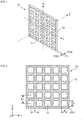
- Fig. 1 is a schematic perspective view of a portion of an example of a filtration filter 10 according to a first embodiment of the present invention.
- Fig. 2 is a schematic view of a portion of the filtration filter 10 of Fig. 1 viewed in the thickness direction.
- the X, Y, and Z directions in the drawing indicate the vertical direction, the horizontal direction, and the thickness direction of the filtration filter 10, respectively.
- Figs. 1 and 2 are enlarged views of a portion of the filtration filter 10.
- the filtration filter 10 includes a filter base portion 12 with a plurality of through-holes 11.
- the filtration filter 10 is a plate-like structure that has a first main surface PS1 on which an object to be filtered contained in a liquid is trapped and a second main surface PS2 facing the first main surface PS1.
- object to be filtered refers to an object to be filtered among objects contained in a liquid.
- an object to be filtered may be a biological substance contained in a liquid.
- biological substance refers to a substance originating from an organism, such as a cell (eukaryote), bacterium (eubacterium), or virus.
- Examples of the cell include induced pluripotent stem cells (iPS cells), ES cells, stem cells, mesenchymal stem cells, mononuclear cells, single cells, cell clusters, suspension cells, adherent cells, neuronal cells, leukocytes, cells for regenerative medicine, autologous cells, cancer cells, circulating cancer cells (CTC), HL-60, HELA, and fungi.
- Examples of the bacterium include Escherichia coli and Mycobacterium tuberculosis.
- Examples of the "liquid” include electrolyte solutions, cell suspensions, and cell culture media.
- the through-holes 11 in the filter base portion 12 are periodically arranged on the first main surface PS1 and the second main surface PS2 of the filtration filter 10. More specifically, the through-holes 11 are arranged in a matrix at regular intervals in the filter base portion 12.
- the through-holes 11 have a square shape when viewed from the first main surface PS1 side of the filtration filter 10, that is, in the Z direction.
- the shape of the through-holes 11 viewed in the thickness direction of the filtration filter 10 (in the Z direction) is not limited to square and may be rectangular, polygonal, circular, or elliptical.
- the through-holes 11 have a rectangular shape (cross-sectional shape) when projected onto a plane perpendicular to the first main surface PS1 of the filtration filter 10. More specifically, the length of one side of each through-hole 11 in the vertical direction (X direction) and the horizontal direction (Y direction) of the filtration filter 10 is larger than the depth of each through-hole 11 in the thickness direction (Z direction) of the filtration filter 10.
- the cross-sectional shape of the through-holes 11 is not limited to rectangular and may be a tapered shape, such as a parallelogram or trapezoid, a symmetric shape, or an asymmetric shape.
- the through-holes 11 are arranged at regular intervals in two array directions parallel to each side of the square when viewed from the first main surface PS1 side of the filtration filter 10 (in the Z direction), that is, in the X direction and in the Y direction in Fig. 1 .
- the through-holes 11 in the square lattice arrangement can have an increased opening ratio and can reduce the resistance of liquid passing through the filtration filter 10. Such a structure can shorten the filtration time and reduce stress on an object to be filtered.
- the arrangement of the through-holes 11 is not limited to the square lattice arrangement and may be a quasi-periodic arrangement or a periodic arrangement.
- the periodic arrangement may be a square or rectangular arrangement, such as a rectangular arrangement with intervals different in two array directions, a triangular lattice arrangement, or a regular triangular lattice arrangement.
- the through-holes 11 may be arranged in any manner, provided that the filter base portion 12 has a plurality of through-holes 11.
- the interval b between the through-holes 11 is appropriately determined according to the type (size, form, property, elasticity) or number of cells to be filtered. As illustrated in Fig. 2 , the interval b between the through-holes 11 refers to the distance between the center of a through-hole 11 and the center of an adjacent through-hole 11 when the through-holes 11 are viewed from the first main surface PS1 side of the filtration filter 10. In the periodic arrangement structure, the interval b between the through-holes 11 may be more than one time and not more than 10 times the length of one side d of the through-holes 11, preferably not more than three times the length of one side d of the through-holes 11.
- the filtration filter 10 may have an opening ratio of 10% or more, preferably 25% or more.
- Such a structure can reduce the resistance of liquid passing through the filtration filter 10. This can shorten the processing time and reduce stress on cells.
- the opening ratio is calculated by (the area occupied by the through-holes 11)/(the projected area of the first main surface PS1 in the absence of the through-holes 11).
- the filtration filter 10 preferably has a thickness of more than 0.1 times and not more than 100 times the size (one side d) of the through-holes 11. More preferably, the filtration filter 10 has a thickness of more than 0.5 times and not more than 10 times the size (one side d) of the through-holes 11.
- Such a structure can reduce the resistance of the filtration filter 10 to liquid and shorten the filtration time. This can reduce stress on an object to be filtered.
- the first main surface PS1 with which a liquid containing an object to be filtered comes into contact preferably has a small surface roughness.
- the surface roughness refers to the average difference between the maximum value and the minimum value measured with a stylus profilometer at five points on the first main surface PS1.
- the surface roughness is preferably smaller than the size of an object to be filtered and is more preferably smaller than half the size of the object to be filtered.
- the openings of the through-holes 11 on the first main surface PS1 of the filtration filter 10 are formed on one plane (XY plane).
- the filter base portion 12, which is a portion where the through-holes 11 are not formed, is continuous and is formed in one piece.
- the openings on the first main surface PS1 communicate with the openings on the second main surface PS2 through a continuous wall surface. More specifically, in the through-holes 11, the openings on the first main surface PS1 can be projected onto the openings on the second main surface PS2. In other words, when the filtration filter 10 is viewed from the first main surface PS1 side, in the through-holes 11, the openings on the first main surface PS1 overlap the openings on the second main surface PS2.
- the inner wall of each through-hole 11 is perpendicular to the first main surface PS1 and the second main surface PS2.
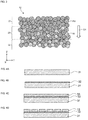
- Fig. 3 is a schematic view of a portion of an example of the filtration filter 10 according to the first embodiment of the present invention.
- Fig. 3 illustrates a portion of an example of the filter base portion 12.
- the filter base portion 12 includes a surface layer 21, a base material 22 formed inside the surface layer 21, and an intermediate layer 23 formed between the surface layer 21 and the base material 22.
- the surface layer 21 is composed mainly of Pd.
- the base material 22 is composed mainly of a PdNi alloy.
- the intermediate layer 23 is composed mainly of a PdNi alloy in which the Pd:Ni ratio changes from the surface layer 21 side toward the base material 22 side.
- the surface layer 21 “composed mainly of Pd” means that the number percentage of Pd atoms in the surface layer 21 is more than 90%.
- the base material 22 “composed mainly of a PdNi alloy” means that the number percentage of Pd atoms in the base material 22 is 70% or more.
- the intermediate layer 23 “composed mainly of a PdNi alloy” means that the number percentage of Pd atoms in the intermediate layer 23 is 50% or more.
- the "PdNi alloy in which the Pd:Ni ratio changes" refers to a PdNi alloy in which the Pd content and the Ni content change stepwise or continuously in the depth direction D1 of the filtration filter 10.
- a change in the Pd:Ni ratio is measured by secondary ion mass spectrometry (SIMS).
- SIMS secondary ion mass spectrometry
- the Pd:Ni ratio can be measured by component analysis performed by SIMS at a predetermined pitch in the depth direction D1 from the surface of the filtration filter 10.
- the surface layer 21 may contain a component other than Pd.
- the surface layer 21 may contain Au, Pt, Fe, Cu, Ti, C, and an oxide thereof.
- the base material 22 and the intermediate layer 23 may contain a component other than PdNi.
- the base material 22 and the intermediate layer 23 may contain Au, Pt, Fe, Cu, Ti, Co, Mo, C, and an oxide thereof.
- the surface layer 21 is a layer on the surface of the filtration filter 10.
- the surface layer 21 covers the base material 22 with the intermediate layer 23 interposed therebetween.
- the surface layer 21 is composed mainly of Pd and does not contain Ni. Thus, the surface layer 21 has a Pd:Ni ratio of 100:0.
- the base material 22 is a main material of the filtration filter 10 and is covered with the surface layer 21 with the intermediate layer 23 interposed therebetween.
- the base material 22 is composed mainly of a PdNi alloy with a constant Pd:Ni ratio.
- the base material 22 has a larger thickness than the surface layer 21 and the intermediate layer 23.
- the base material 22 has a Pd:Ni ratio in the range of 75:25 to 85:15.
- the PdNi alloy of the base material 22 has a Pd:Ni ratio of 80:20.
- the intermediate layer 23 is a layer between the surface layer 21 and the base material 22.
- the intermediate layer 23 is composed mainly of a PdNi alloy in which the Pd:Ni ratio changes.
- the Pd:Ni ratio changes in the depth direction D1 of the filtration filter 10. More specifically, in the intermediate layer 23, the ratio of Ni to Pd of the PdNi alloy increases from the surface layer 21 toward the base material 22.
- the Pd:Ni ratio of the intermediate layer 23 changes in the range of 100:0 to 75:25. In the first embodiment, the Pd:Ni ratio of the intermediate layer 23 changes from 100:0 to 80:20 as the depth increases in the depth direction D1 of the filtration filter 10.
- Ni is dispersed.
- the interface between Pd and Ni is not continuous and is dispersed.
- the intermediate layer 23 has a larger thickness than the surface layer 21.
- the interface between Pd and Ni is easily dispersed in the thickness direction of the filtration filter 10 (in the Z direction). This can reduce corrosion at the interface between Pd and Ni.
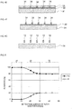
- FIG. 4A to 4G illustrate an example of a production process of the filtration filter 10 according to the first embodiment of the present invention.
- a substrate 31 made of silicon or the like is prepared.
- the substrate 31 may be subjected to surface cleaning, for example.
- a Cu film 32 500 nm in thickness is formed on the substrate 31.
- the Cu film 32 is formed by sputtering with a sputter deposition apparatus.
- the Cu film 32 may be formed by vapor deposition with a vapor deposition apparatus.
- a Ti film 50 nm in thickness may be formed between the substrate 31 and the Cu film 32.
- a resist is applied to the Cu film 32 and is dried to form a resist film 33 2 ⁇ m in thickness.
- a photosensitive positive liquid resist (Pfi-3A manufactured by Sumitomo Chemical Co., Ltd.) is applied to the Cu film 32 with a spin coater.
- the spin coater conditions include 1140 rpm and 30 seconds, for example.
- the resist is heated and dried on a hot plate to form the resist film 33 2.0 ⁇ m in thickness.
- the hot plate conditions include a heating temperature of 90°C and a heating time of 90 seconds, for example.
- the resist film 33 is exposed to light and is developed to remove a portion of the resist film 33 corresponding to the filter base portion 12.
- an i-line stepper Pfi-37A manufactured by Canon Inc.
- Development is performed with a paddle developing apparatus.
- Tetramethylammonium hydroxide (TMAH) is used as a developer. Exposure to light and development are followed by washing with water and drying.
- electroplating is performed in a PdNi plating bath with an electroplating apparatus.
- a PdNi plating film 34 is formed on the portion from which the resist film 33 has been removed.
- the electroplating conditions include a current density of 1 A/dm 2 , an electric quantity of 4 AM, a pH of the plating solution of 7.5, and a plating thickness of 1.6 ⁇ m, for example.
- the resist film 33 is stripped with a stripping liquid NMP (N-methyl-2-pyrrolidone) in a resist stripping apparatus capable of high-pressure spray treatment. Subsequently, the PdNi plating film 34 is washed with IPA (isopropyl alcohol), is washed with water, and is dried.
- NMP N-methyl-2-pyrrolidone
- the PdNi plating film 34 is removed from the substrate 31, and Ni in the surface layer of the PdNi plating film 34 is dissolved.
- the filter base portion 12 is formed.
- the immersion treatment of the PdNi plating film 34 in the aqueous acetic acid hydrogen peroxide can gradually dissolve Ni from the surface of the PdNi plating film 34 toward the inside.
- Ni in the PdNi plating film 34 easily comes into contact with the aqueous acetic acid hydrogen peroxide and is easily dissolved.
- the amount of dissolved Ni decreases gradually from the surface of the PdNi plating film 34 toward the inside.
- the aqueous acetic acid hydrogen peroxide dissolves Ni, and the surface layer 21 composed mainly of Pd is formed.
- the amount of Ni dissolved in the aqueous acetic acid hydrogen peroxide decreases gradually from the surface layer 21 of the filter base portion 12 in the depth direction D1.
- the intermediate layer 23 thus formed is composed mainly of a PdNi alloy in which the Pd:Ni ratio changes.
- a portion of the PdNi plating film 34 in which Ni is not dissolved in the aqueous acetic acid hydrogen peroxide becomes the base material 22.
- the filtration filter 10 which includes the surface layer 21 composed mainly of Pd, the base material 22 composed mainly of a PdNi alloy, and the intermediate layer 23 composed mainly of a PdNi alloy in which the Pd:Ni ratio changes formed between the surface layer 21 and the base material 22.
- Example 1 is described below.
- a portion of the filter base portion 12 produced by the above production method was used as a sample, and the Pd:Ni ratio in the depth direction D1 of the filter base portion 12 was analyzed.
- the PdNi plating film 34 with a Pd:Ni ratio of 80:20 was immersed in the aqueous acetic acid hydrogen peroxide to form the filter base portion 12.
- the outer surface of the filter base portion 12 was irradiated with primary ions.
- the surface at the position where the measuring apparatus detected the first metal information was assumed to have a depth of 0 nm.
- the surface with a depth of 0 nm is defined as the surface of the filter base portion 12.
- Fig. 5 shows analytical data of the Pd:Ni ratio of the filter base portion 12 of Example 1 in the depth direction D1.
- the surface layer 21 is formed in a region with a depth in the range of 0 to 10 nm from the surface of the filter base portion 12.
- the surface layer 21 has a thickness of 10 nm.
- Pd constitutes 100%
- Ni constitutes 0%.
- the surface layer 21 has a Pd:Ni ratio of 100:0.
- the intermediate layer 23 is formed in a region with a depth of more than 10 nm and 30 nm or less from the surface of the filter base portion 12. More preferably, the intermediate layer 23 is formed in a region with a depth in the range of 20 to 30 nm from the surface of the filtration filter 10. Thus, the intermediate layer 23 has a thickness in the range of 10 to 20 nm.
- the Pd content decreases from 100% to 80%, and the Ni content increases from 0% to 20%.
- the Pd:Ni ratio changes in the range of 100:0 to 80:20.
- the region in which the intermediate layer 23 is formed is not limited to the region in Example 1.
- the intermediate layer 23 is formed at least in a region with a depth in the range of 20 to 30 nm from the surface of the filtration filter 10.
- the intermediate layer 23 may be formed in a region with a depth of more than 10 nm and 40 nm or less from the surface of the filter base portion 12.
- the intermediate layer 23 may also be formed in a region with a depth of more than 10 nm and 35 nm or less from the surface of the filter base portion 12.
- the ratio of Ni to Pd in the PdNi alloy in the intermediate layer 23 increases with the depth in the depth direction D1 of the filtration filter 10.
- the ratio of Ni to Pd in the PdNi alloy in the intermediate layer 23 increases from the surface layer 21 side toward the base material 22 side.
- the base material 22 is formed in a region with a depth of more than 30 nm from the surface of the filter base portion 12.
- Pd constitutes 80%
- Ni constitutes 20%.
- the base material 22 has a constant Pd:Ni ratio of 80:20.
- Example 1 component analysis was performed on the surface of the filter base portion 12.
- the analysis was performed by X-ray photoelectron spectroscopy (XPS). Under analytical conditions, the analysis was performed on the surface of the PdNi plating film 34 before immersed in the aqueous acetic acid hydrogen peroxide (see Fig. 4F ) and on the surface of the filter base portion 12 after immersed in the aqueous acetic acid hydrogen peroxide (see Fig. 4G ).
- XPS X-ray photoelectron spectroscopy
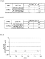
- Fig. 6 is a table of component analysis results of the surface of the filter base portion 12 of Example 1. As shown in Fig. 6 , in Example 1, the Ni content is 7% and the Pd content is 93% on the surface of the PdNi plating film 34 before immersed in the aqueous acetic acid hydrogen peroxide.
- Example 1 when the PdNi plating film 34 is immersed in the aqueous acetic acid hydrogen peroxide to form the filter base portion 12, the Ni content becomes 0% and the Pd content becomes 100% on the surface of the filter base portion 12.
- Example 1 The analysis results in Example 1 show that the PdNi plating film 34 can be immersed in the aqueous acetic acid hydrogen peroxide to remove Ni from the surface layer of the PdNi plating film 34.
- the filter base portion 12 including the surface layer 21 composed mainly of Pd could be produced.
- Example 2 the filter base portion 12 was subjected to the component analysis at a Pd:Ni ratio different from the Pd:Ni ratio in Example 1.
- the PdNi plating film 34 with a Pd:Ni ratio of 50:50 was immersed in the aqueous acetic acid hydrogen peroxide to form the filter base portion 12.
- the analysis method and analytical conditions in Example 2 are the same as those in Example 1.
- Fig. 7 is a table of component analysis results of the surface of the filter base portion 12 of Example 2. As shown in Fig. 7 , in Example 2, the Ni content is 11% and the Pd content is 89% on the surface of the PdNi plating film 34 before immersed in the aqueous acetic acid hydrogen peroxide.
- Example 2 when the PdNi plating film 34 is immersed in the aqueous acetic acid hydrogen peroxide to form the filter base portion 12, the Ni content becomes 0% and the Pd content becomes 100% on the surface of the filter base portion 12.
- Example 2 The analysis results in Example 2 also show that the PdNi plating film 34 could be immersed in the aqueous acetic acid hydrogen peroxide to remove Ni from the surface layer of the PdNi plating film 34 and thereby produce the filter base portion 12 including the surface layer 21 composed mainly of Pd.
- Example 3 is described below.
- the filtration filter 10 was produced by the above production method at different pH values of the plating solution for the PdNi plating bath.
- the pH values of the plating solution were 7.2, 7.5, and 7.9.
- the filtration filter 10 was subjected to an elution test. In the elution test, a portion with a surface area of 1 cm 2 in the filtration filter 10 was immersed in 10 ml of PBS and was kept at 37°C in an incubator for one week.
- the elution concentrations of Pd and Ni were analyzed with an ICP-MS (manufactured by Agilent Technologies). The detection limit of the ICP-MS for Pd and Ni is 0.005 ⁇ g/ml.
- Fig. 8 is a graph of analysis results of the elution concentration of Ni in Example 3.
- Fig. 9 is a graph of analysis results of the elution concentration of Pd in Example 3.
- Figs. 8 and 9 show that the elution concentrations of Pd and Ni were below the detection limit of the ICP-MS for Pd and Ni. This indicates that Pd and Ni are not eluted in Example 3.
- the pH value of the plating solution ranges from 7.0 to 8.5. More preferably, the pH value of the plating solution ranges from 7.2 to 7.9.
- Example 4 is described below.
- the filtration filter 10 was produced by the above production method at different current densities of the PdNi plating bath. The current densities ranged from 2.9 to 14.5 [A/dm 2 ].
- the filtration filter 10 was subjected to an elution test. In the elution test, a portion with a surface area of 1 cm 2 in the filtration filter 10 was immersed in 10 ml of PBS and was kept at 37°C in an incubator for one week. In the same manner as in Example 3, the elution concentrations of Pd and Ni were analyzed with the ICP-MS (manufactured by Agilent Technologies).
- Fig. 10 is a graph of analysis results of the elution concentration of Ni in Example 4.
- Fig. 11 is a graph of analysis results of the elution concentration of Pd in Example 4.
- Figs. 10 and 11 show that the elution concentrations of Pd and Ni were below the detection limit of the ICP-MS for Pd and Ni. This indicates that Pd and Ni are not eluted in Example 4.
- the current density ranges from 0.5 to 30 [A/dm 2 ]. More preferably, the current density ranges from 2.9 to 14.5 [A/dm 2 ].
- Example 5 is described below.
- the PdNi plating film 34 was formed by the above production method at different concentration ratios of Pd to Ni in the PdNi plating bath.
- the Pd concentration ratio ranged from 52% to 80%.
- the Pd concentration ratio is calculated using the formula Pd/(Pd + Ni).
- the Ni concentration ratio is calculated using the formula Ni/(Pd + Ni).
- the Pd concentration ratio of the PdNi plating film 34 formed by changing the Pd concentration ratio was analyzed to examine the effect of changing the Pd concentration ratio of the plating bath on the composition of the PdNi plating film 34.
- Fig. 12 is a graph of an example of the relationship between the Pd concentration ratio of the plating film 34 and the Pd concentration ratio in Example 5.
- Fig. 12 shows that the concentration ratio of Pd to Ni in the plating bath in the formation of the PdNi plating film 34 can be controlled to change the component ratio of the PdNi plating film 34.
- each PdNi plating film 34 formed at the Pd concentration ratio shown in Fig. 12 was subjected to the XPS component analysis of the surface layer.
- Fig. 13 is a table of analysis results of the Ni component in the surface layer of the PdNi plating film 34 at each component ratio in Example 5. ND in Fig. 13 indicates that the value is below the detection limit of XPS.
- Fig. 13 shows that the Ni ratio of the surface layer of the PdNi plating film 34 was ND at Pd:Ni ratios of 52:48, 58:42, 66:34, 68:32, and 80:20. This indicates that Ni is not detected in the surface layer of the PdNi plating film 34 in Example 5.
- Example 6 is described below.
- the filtration filter 10 was produced by the above production method at different surface roughnesses Ra of the PdNi plating film 34.
- the surface roughness Ra was changed by adjusting the pH value of the plating solution, the current density, the substrate base material, and the film thickness in the PdNi plating bath.
- the surface roughness Ra was 0.02, 0.94, or 1.98 ⁇ m.
- the filtration filter 10 was subjected to an elution test. In the elution test, a portion with a surface area of 1 cm 2 in the filtration filter 10 was immersed in 10 ml of PBS and was kept at 37°C in an incubator for one week. In the same manner as in Examples 3 and 4, the elution concentration of Ni was analyzed with the ICP-MS (manufactured by Agilent Technologies).
- Fig. 14 is a graph of analysis results of the elution concentration of Ni in Example 6. Fig. 14 shows that the elution concentration of Ni was below the detection limit of the ICP-MS for Ni. This indicates that Ni is not eluted in Example 6.
- the surface roughness Ra is 2.5 ⁇ m or less. More preferably, the surface roughness Ra is 1.98 ⁇ m or less.
- the immersion of the PdNi plating film 34 in the aqueous acetic acid hydrogen peroxide dissolves and eliminates Ni on the surface layer and consequently increases the Pd content of the surface layer 21.
- the elution test of the PdNi plating film 34 in this state shows that the elution concentration of Ni is below the detection limit (0.01 ⁇ g/ml).
- the immersion in the aqueous acetic acid hydrogen peroxide causes sufficient liquid exchange with the aqueous acetic acid hydrogen peroxide on the surface of the PdNi plating film 34, completely eliminates Ni from the surface layer 21, and increases the Pd content of the surface layer 21.
- a portion of fine asperities of the surface layer 21 is not sufficiently covered with the aqueous acetic acid hydrogen peroxide, and liquid exchange is less likely to occur at the portion. It may be difficult to eliminate Ni and increase the Pd content at the portion of the surface layer 21.
- the elution test of the PdNi plating film 34 in this state shows that the Ni concentration was increased probably due to the elution of Ni remaining in the surface layer 21.
- Example 7 is described below.
- the filtration filter 10 was produced by the above production method at different immersion times of the PdNi plating film 34 in the aqueous acetic acid hydrogen peroxide.
- the PdNi plating film 34 in Example 7 has a Pd:Ni ratio of 9:1.
- the immersion time was 0 seconds, 10 seconds, 30 seconds, 1 minute, 5 minutes, 30 minutes, 1 hour, and 2 hours at room temperature.
- the aqueous acetic acid hydrogen peroxide is acetic acid 5%:hydrogen peroxide 5%:pure water 90%.
- Fig. 15 is a table of analysis results of the Ni component in the surface layer of the filtration filter 10 in Example 7.
- Fig. 15 shows that an immersion time of 1 minute or more can result in the Ni content of 0% in the surface layer of the filtration filter 10.
- Example 8 is described below.
- the compositions of samples A1 and A2 of the filtration filter 10 produced by the above production method were examined.
- TEM observation and EDX mapping were performed.
- the TEM observation was performed with an FE-TEM (JEOL Ltd.: JEM-F200).
- the TEM measurement conditions included accelerating voltage: 200 kV, focusing lens aperture: #2, and pretreatment: Pt coating.
- the EDX mapping was performed with Noran system 7 (Wakenyaku Co., Ltd.).
- the EDX measurement conditions included spot diameter: ⁇ 1.0 nm, time constant: Rate 1, and the number of scans: 100.
- the sample A1 of the filtration filter 10 was prepared at a current density of 2.9 [A/dm 2 ].
- the sample A2 was prepared at a current density of 14.5 [A/dm 2 ].
- the immersion time of the PdNi plating film in the aqueous acetic acid hydrogen peroxide was 2 hours.
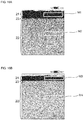
- Fig. 16A is an EDX mapping of the sample A1 in Example 8.
- a portion M1 indicates a portion of the surface layer 21 of the sample A1
- a portion M2 indicates a portion of the base material of the sample A1.
- the intermediate layer 23 of the sample A1 in Fig. 16A is formed in a region at a distance of approximately 32 nm from the surface.
- the portion M2 of the base material 22 in Fig. 16A is a region at a distance of approximately 106 nm from the surface.
- Fig. 16B is an EDX mapping of the sample A2 in Example 8.
- a portion M3 indicates a portion of the surface layer 21 of the sample A2
- a portion M4 indicates a portion of the base material 22 of the sample A2.
- the intermediate layer 23 of the sample A2 in Fig. 16B is formed in a region at a distance of approximately 22.5 nm from the surface.
- the portion M4 of the base material 22 in Fig. 16B was a region at a distance of approximately 97 nm from the surface.
- the EDX quantitative analysis of the portion M1 in Fig. 16A showed Pd: 98.7%, Ni: 0.6%, and O: 0.7%.
- the EDX quantitative analysis of the portion M2 in Fig. 16A showed Pd: 81.6%, Ni: 18.4%, and O: 0%. It should be noted that values of less than 1% include noise.
- the EDX quantitative analysis of the portion M3 in Fig. 16B showed Pd: 98.9%, Ni: 1.1%, and O: 0%.
- the EDX quantitative analysis of the portion M4 in Fig. 16B showed Pd: 76.6%, Ni: 23.4%, and O: 0%. It should be noted that values of less than 1% include noise.
- Figs. 16A and 16B show that Ni in the surface layer portion was eliminated in the samples A1 and A2 of Example 8.
- Ni in the surface layer portion was eliminated in the filtration filters 10 produced at a current density of 2.9 [A/dm 2 ] and at a current density of 14.5 [A/dm 2 ].
- the difference in the Pd:Ni ratio between the portion M2 (base material portion) of the sample A1 and the portion M4 (base material portion) of the sample A2 is probably due to the difference in current density.
- the filtration filter 10 according to the first embodiment has the following advantages.
- the filtration filter 10 includes the surface layer 21, the base material 22 formed inside the surface layer 21, and the intermediate layer 23 formed between the surface layer 21 and the base material 22.
- the surface layer 21 is composed mainly of Pd
- the base material 22 is composed mainly of a PdNi alloy
- the intermediate layer 23 is composed mainly of a PdNi alloy in which the Pd:Ni ratio changes from the surface layer 21 side toward the base material 22 side.
- the filtration filter 10 with such a structure can have improved corrosion resistance.
- a filtration filter according to Comparative Example 1 is described below.
- a surface of a base material 122 formed of a non-precious metal is coated with a noble metal by plating to form a surface layer 121 of the noble metal on the surface of the base material 122 of the non-precious metal.
- the surface layer 121 is composed mainly of Pd
- the base material 122 is composed mainly of Ni.
- Fig. 17 is a schematic view of a portion of an example of a filtration filter 110 according to Comparative Example 1.
- the surface layer 121 composed mainly of a noble metal Pd is formed on the base material 122 composed mainly of a non-precious metal Ni.
- the plating forms defects 150 in the surface layer 121 due to impurities adhering to the surface of the base material 122 and/or due to surface roughness.
- a liquid such as an electrolyte solution, easily comes into contact with the base material 122 through the defects 150 in the surface layer 121. This makes it difficult to prevent the base material 122 from being eluted through the defects 150.
- the surface layer 121, the base material 122, and the electrolyte solution in contact with the interface between the surface layer 121 and the base material 122 tend to form a local cell, which causes an anodic reaction on the surface of the base material 122 made of the non-precious metal (Ni) and may result in corrosion of the base material 122. Furthermore, due to the continuous interface between the surface layer 121 and the base material 122, corrosion of the base material 122 spreads easily over the entire base material 122.
- the base material 122 When the surface layer 121 is damaged and peeled off, the base material 122 is easily exposed and is easily eluted when coming into contact with the electrolyte solution.
- the intermediate layer 23 is formed between the surface layer 21 and the base material 22.
- the Pd:Ni ratio changes from the surface layer 21 side toward the base material 22 side.
- the interface between Pd and Ni is dispersed in the intermediate layer 23 of the filtration filter 10. This can prevent Ni from being eluted through defects in the surface layer 21 when the filtration filter 10 comes into contact with a liquid, such as an electrolyte solution.
- the intermediate layer 23 formed between the surface layer 21 and the base material 22 can reduce the elution of the base material 22.
- the ratio of Ni to Pd in the intermediate layer 23 increases with the depth in the depth direction D1 of the filtration filter 10.
- Such a structure can separate most of the Ni in the intermediate layer 23 from the surface layer 21 and reduce the elution and corrosion of Ni caused by contact with an electrolyte solution. This can further improve the corrosion resistance of the filtration filter 10.
- the intermediate layer 23 has a larger thickness than the surface layer 21.
- Such a structure enables Ni to be further dispersed in the depth direction D1 of the filtration filter 10.
- Such a structure can also further separate the base material 22 from the surface layer 21 and can further reduce the elution and corrosion of the base material 22. This can further improve the corrosion resistance of the filtration filter 10.
- the intermediate layer 23 is formed in a region with a depth of more than 10 nm and 30 nm or less from the surface of the filtration filter 10. More preferably, the intermediate layer 23 is formed in a region with a depth in the range of 20 to 30 nm from the surface of the filtration filter 10.
- the filtration filter 10 with such a structure can have further improved corrosion resistance.
- the base material 22 is formed at a position deeper than the intermediate layer 23.
- the permeation of an electrolyte solution decreases with increasing depth, and the chance of the electrolyte solution coming into contact with the base material decreases with increasing depth.
- the filtration filter 10 with such a structure can therefore have improved corrosion resistance.
- the base material 22 has a Pd:Ni ratio of 80:20, and the intermediate layer 23 has a Pd:Ni ratio varying in the range of 100:0 to 80:20.
- the filtration filter 10 with such a structure can have further improved corrosion resistance.
- the filtration filter 10 composed of Pd and the PdNi alloy is described in the first embodiment, the present invention is not limited to this embodiment.
- the filtration filter 10 may be made of a metal or alloy containing a noble metal other than Pd and a non-precious metal other than Ni.
- the present invention is not limited to this embodiment.
- the intermediate layer 23 may include a portion where the ratio of Ni to Pd in the PdNi alloy is constant and/or decreases.
- the filtration filter 10 with such a structure can also have improved corrosion resistance.
- the intermediate layer 23 has a larger thickness than the surface layer 21 in the first embodiment, the present invention is not limited to this embodiment.
- the intermediate layer 23 may have a thickness smaller than or equal to the thickness of the surface layer 21.
- the filtration filter 10 with such a structure can also have improved corrosion resistance.
- the filtration filter of the first embodiment is used as a mesh of a mesh nebulizer.
- Major differences between the second embodiment and the first embodiment are described below.
- the same or equivalent constituents as the constituents of the first embodiment are denoted by the same reference numerals and letters.
- the constituents described in the first embodiment are omitted in the second embodiment.
- the second embodiment aims to improve the corrosion resistance of the mesh of the mesh nebulizer.
- Fig. 18 is a schematic partial cross-sectional view of an example of a mesh 50 according to the second embodiment of the present invention.
- the mesh 50 includes a first base portion 12 and a second base portion 13.
- First through-holes 11 and the first base portion 12 described in the second embodiment correspond to the through-holes 11 and the filter base portion 12 in the first embodiment.
- the second base portion 13 is located on a first main surface PS1 side of the first base portion 12.
- the second base portion 13 is a plate-like member having a third main surface PS3 and a fourth main surface PS4 facing the third main surface PS3.
- the second base portion 13 has a smaller thickness than the first base portion 12.
- the second base portion 13 and the first base portion 12 form a single body.
- the second base portion 13 has a plurality of second through-holes 14.
- the second through-holes 14 are periodically arranged on the third main surface PS3 and the fourth main surface PS4 of the second base portion 13. More specifically, the second through-holes 14 are arranged in a matrix at regular intervals in the second base portion 13.
- the second through-holes 14 have a square lattice arrangement when viewed from the third main surface PS3 side (in the Z direction).
- the arrangement of the second through-holes 14 is not limited to the square lattice arrangement and may be a quasi-periodic arrangement or a periodic arrangement.
- the periodic arrangement may be a square or rectangular arrangement, such as a rectangular arrangement with intervals different in two array directions, a triangular lattice arrangement, or a regular triangular lattice arrangement.
- the second through-holes 14 may be any array of through-holes in the second base portion 13.
- each of the second through-holes 14 has a square shape when viewed from the third main surface PS3 side (in the Z direction).
- the shape of the second through-holes 14 viewed from the third main surface PS3 side (in the Z direction) is not limited to square and may be rectangular, polygonal, circular, or elliptical.
- the second through-holes 14 have a rectangular shape (cross-sectional shape) when projected onto a plane perpendicular to the third main surface PS3 of the second base portion 13.
- the cross-sectional shape of the second through-holes 14 is not limited to rectangular and may be a tapered shape, such as a parallelogram or trapezoid, a symmetric shape, or an asymmetric shape.
- the second through-holes 14 have a smaller size than the first through-holes 11.
- the length of one side of the second through-holes 14 in the vertical direction (X direction) and the horizontal direction (Y direction) of the mesh 50 is smaller than the length of one side of the first through-holes 11.
- the second through-holes 14 have a circular shape, the second through-holes 14 have a smaller diameter than the first through-holes 11.
- the second through-holes 14 connect to the first through-holes 11. In other words, the second through-holes 14 communicate with the first through-holes 11.
- the mesh 50 includes a surface layer 21, a base material 22 formed inside the surface layer 21, and an intermediate layer 23 formed between the surface layer 21 and the base material 22.
- the surface layer 21 of the mesh 50 is composed mainly of Pd.
- the base material 22 of the mesh 50 is composed mainly of a PdNi alloy.
- the intermediate layer 23 of the mesh 50 is composed mainly of a PdNi alloy in which the Pd:Ni ratio changes from the surface layer 21 side toward the base material 22 side.
- Figs. 19A to 19K illustrate an example of a production process of the mesh 50 according to the second embodiment of the present invention.
- a substrate 41 made of silicon or the like is prepared.
- the substrate 41 may be subjected to surface cleaning, for example.
- a Cu film 42 500 nm in thickness is formed on the substrate 41.
- the Cu film 42 is formed by sputtering with a sputter deposition apparatus.
- the Cu film 42 may be formed by vapor deposition with a vapor deposition apparatus.
- a Ti film 50 nm in thickness may be formed between the substrate 41 and the Cu film 42.
- a resist is applied to the Cu film 42 and is dried to form a resist film 43 2 ⁇ m in thickness.
- a photosensitive positive liquid resist (Pfi-3A manufactured by Sumitomo Chemical Co., Ltd.) is applied to the Cu film 42 with a spin coater.
- the spin coater conditions include 1140 rpm and 30 seconds, for example.
- the resist is heated and dried on a hot plate to form the resist film 43 2.0 ⁇ m in thickness.
- the hot plate conditions include a heating temperature of 90°C and a heating time of 90 seconds, for example.
- the resist film 43 is exposed to light and is developed to remove a portion of the resist film 43 corresponding to the second base portion 13.
- an i-line stepper Pfi-37A manufactured by Canon Inc.
- Development is performed with a paddle developing apparatus.
- Tetramethylammonium hydroxide (TMAH) is used as a developer. Exposure to light and development are followed by washing with water and drying.
- electroplating is performed in a PdNi plating bath with an electroplating apparatus.
- a PdNi plating film 44 is formed on the portion from which the resist film 43 has been removed.
- the electroplating conditions include a current density of 1 A/dm, an electric quantity of 4 AM, a pH of the plating solution of 7.5, and a plating thickness of 1.6 ⁇ m, for example.
- the resist film 43 is stripped with a stripping liquid NMP (N-methyl-2-pyrrolidone) in a resist stripping apparatus capable of high-pressure spray treatment.
- NMP N-methyl-2-pyrrolidone
- the PdNi plating film 44 is washed with IPA (isopropyl alcohol), is washed with water, and is dried.
- a dry film resist 45 is laminated to the PdNi plating film 44.
- the dry film resist 45 has a thickness of 50 ⁇ m.
- the upper and lower roll temperatures in the lamination are 100°C, and the feed rate is 0.4 m/s.
- the dry film resist 45 is exposed to light and is developed to remove a portion of the dry film resist 45 corresponding to the first base portion 12.
- the dry film resist 45 is exposed to light with an aligner and is developed by spray development.
- the developer is a 3% sodium carbonate solution.
- electroplating is performed in a PdNi plating bath with an electroplating apparatus.
- a PdNi plating film 46 is formed on the portion from which the dry film resist 45 has been removed.
- Immersion in 5% hydrochloric acid for 1 minute and washing with water were performed as plating pretreatment.
- PdNi electroplating was performed with an electroplating apparatus.
- the electroplating conditions include a current density of 1 A/dm 2 , an electric quantity of 4 AM, a pH of the plating solution of 7.5, and a plating thickness of 1.6 ⁇ m, for example.
- the resist film 45 is stripped with a stripping liquid NMP (N-methyl-2-pyrrolidone) in a resist stripping apparatus.
- NMP N-methyl-2-pyrrolidone
- the PdNi plating films 44 and 46 are removed from the substrate 41, and Ni in the surface layer of the PdNi plating films 44 and 46 is dissolved.
- the first base portion 12 and the second base portion 13 are formed.
- the immersion treatment of the PdNi plating films 44 and 46 in the aqueous acetic acid hydrogen peroxide gradually dissolves Ni from the surface of the PdNi plating films 44 and 46 toward the inside.
- Ni in the PdNi plating films 44 and 46 easily comes into contact with the aqueous acetic acid hydrogen peroxide and is easily dissolved.
- it becomes more difficult for Ni in the PdNi plating films 44 and 46 at a deeper position to come into contact with the aqueous acetic acid hydrogen peroxide and to dissolve.
- the amount of dissolved Ni decreases gradually from the surface of the PdNi plating film 44 and 46 toward the inside.
- the aqueous acetic acid hydrogen peroxide dissolves Ni, and the surface layer 21 composed mainly of Pd is formed.
- the amount of Ni dissolved in the aqueous acetic acid hydrogen peroxide decreases gradually from the surface layer 21 of the first base portion 12 and the second base portion 13 in the depth direction D1.
- the intermediate layer 23 thus formed is composed mainly of a PdNi alloy in which the Pd:Ni ratio changes.
- a portion of the PdNi plating films 44 and 46 in which Ni is not dissolved in the aqueous acetic acid hydrogen peroxide becomes the base material 22.
- the mesh 50 which includes the surface layer 21 composed mainly of Pd, the base material 22 composed mainly of a PdNi alloy, and the intermediate layer 23 composed mainly of a PdNi alloy in which the Pd:Ni ratio changes formed between the surface layer 21 and the base material 22.
- the mesh 50 according to the second embodiment has the following advantages.
- the mesh 50 includes the surface layer 21, the base material 22 formed inside the surface layer 21, and the intermediate layer 23 formed between the surface layer 21 and the base material 22.
- the surface layer 21 is composed mainly of Pd
- the base material 22 is composed mainly of a PdNi alloy
- the intermediate layer 23 is composed mainly of a PdNi alloy in which the Pd:Ni ratio changes from the surface layer 21 side toward the base material 22 side.
- the mesh 50 with such a structure can have improved corrosion resistance.
- the mesh 50 includes the first base portion 12 and the second base portion 13 in the second embodiment, the present invention is not limited to this embodiment. It is only necessary that the mesh 50 includes the surface layer 21, the base material 22, and the intermediate layer 23. The mesh 50 may include no second base portion 13.
- the filtration filter according to the present invention is useful in filtering an object to be filtered in a liquid.
Landscapes
- Chemical & Material Sciences (AREA)
- Engineering & Computer Science (AREA)
- Life Sciences & Earth Sciences (AREA)
- Organic Chemistry (AREA)
- Health & Medical Sciences (AREA)
- Wood Science & Technology (AREA)
- Bioinformatics & Cheminformatics (AREA)
- Zoology (AREA)
- Biotechnology (AREA)
- Chemical Kinetics & Catalysis (AREA)
- General Engineering & Computer Science (AREA)
- Sustainable Development (AREA)
- Microbiology (AREA)
- Biochemistry (AREA)
- Biomedical Technology (AREA)
- General Health & Medical Sciences (AREA)
- Genetics & Genomics (AREA)
- Metallurgy (AREA)
- Materials Engineering (AREA)
- General Chemical & Material Sciences (AREA)
- Mechanical Engineering (AREA)
- Molecular Biology (AREA)
- Geology (AREA)
- Electrochemistry (AREA)
- Filtering Materials (AREA)
- Separation Using Semi-Permeable Membranes (AREA)
- Exposure And Positioning Against Photoresist Photosensitive Materials (AREA)
- Apparatus Associated With Microorganisms And Enzymes (AREA)
Abstract
Description
- The present invention relates to a filtration filter.
- For example, filters for trapping biological materials described in
Patent Document 1 are known as filtration filters. In the filters described inPatent Document 1, a surface of a filter for trapping a biological material made of a metal other than gold is plated with gold, and the gold plating is electroless gold plating. - Patent Document 1:
Japanese Unexamined Patent Application Publication No. 2018-88932 - However, there is room for improvement in the corrosion resistance of the filters described in
Patent Document 1. - It is an object of the present invention to provide a filtration filter with improved corrosion resistance. Solution to Problem
- A filtration filter according to one aspect of the present invention includes
a surface layer,
a base material formed inside the surface layer; and
an intermediate layer formed between the surface layer and the base material,
wherein the surface layer is composed mainly of Pd,
the base material is composed mainly of a PdNi alloy, and
the intermediate layer is composed mainly of a PdNi alloy in which a Pd:Ni ratio changes from a surface layer side toward a base material side. - The present invention can provide a filtration filter with improved corrosion resistance.
-
- [
Fig. 1] Fig. 1 is a schematic perspective view of a portion of an example of a filtration filter according to a first embodiment of the present invention. - [
Fig. 2] Fig. 2 is a schematic view of a portion of the filtration filter ofFig. 1 viewed in the thickness direction. - [
Fig. 3] Fig. 3 is a schematic view of a portion of an example of the filtration filter according to the first embodiment of the present invention. - [
Fig. 4A] Fig. 4A is a schematic view of an example of a production process of the filtration filter according to the first embodiment of the present invention. - [
Fig. 4B] Fig. 4B is a schematic view of an example of a production process of the filtration filter according to the first embodiment of the present invention. - [
Fig. 4C] Fig. 4C is a schematic view of an example of a production process of the filtration filter according to the first embodiment of the present invention. - [
Fig. 4D] Fig. 4D is a schematic view of an example of a production process of the filtration filter according to the first embodiment of the present invention. - [
Fig. 4E] Fig. 4E is a schematic view of an example of a production process of the filtration filter according to the first embodiment of the present invention. - [
Fig. 4F] Fig. 4F is a schematic view of an example of a production process of the filtration filter according to the first embodiment of the present invention. - [
Fig. 4G] Fig. 4G is a schematic view of an example of a production process of the filtration filter according to the first embodiment of the present invention. - [
Fig. 5] Fig. 5 is analytical data of the Pd:Ni ratio of a filter base portion of Example 1 in the depth direction. - [
Fig. 6] Fig. 6 is a table of component analysis results of a surface layer of the filter base portion of Example 1. - [
Fig. 7] Fig. 7 is a table of component analysis results of a surface layer of a filter base portion of Example 2. - [
Fig. 8] Fig. 8 is a graph of analysis results of the elution concentration of Ni in Example 3. - [
Fig. 9] Fig. 9 is a graph of analysis results of the elution concentration of Pd in Example 3. - [
Fig. 10] Fig. 10 is a graph of analysis results of the elution concentration of Ni in Example 4. - [
Fig. 11] Fig. 11 is a graph of analysis results of the elution concentration of Pd in Example 4. - [
Fig. 12] Fig. 12 is a graph of an example of the relationship between the Pd concentration ratio of a plating film and the Pd concentration ratio in Example 5. - [
Fig. 13] Fig. 13 is a table of analysis results of a Ni component in a surface layer of a PdNi plating film at each component ratio in Example 5. - [
Fig. 14] Fig. 14 is a graph of analysis results of the elution concentration of Ni in Example 6. - [
Fig. 15] Fig. 15 is a table of analysis results of a Ni component in a surface layer of a filtration filter in Example 7. - [
Fig. 16A] Fig. 16A is an EDX mapping of a sample A1 in Example 8. - [
Fig. 16B] Fig. 16B is an EDX mapping of a sample A2 in Example 8. - [
Fig. 17] Fig. 17 is a schematic view of a portion of an example of a filtration filter according to Comparative Example 1. - [
Fig. 18] Fig. 18 is a schematic partial cross-sectional view of an example of a mesh according to a second embodiment of the present invention. - [
Fig. 19A] Fig. 19A is a schematic view of an example of a production process of the mesh according to the second embodiment of the present invention. - [
Fig. 19B] Fig. 19B is a schematic view of an example of a production process of the mesh according to the second embodiment of the present invention. - [
Fig. 19C] Fig. 19C is a schematic view of an example of a production process of the mesh according to the second embodiment of the present invention. - [
Fig. 19D] Fig. 19D is a schematic view of an example of a production process of the mesh according to the second embodiment of the present invention. - [
Fig. 19E] Fig. 19E is a schematic view of an example of a production process of the mesh according to the second embodiment of the present invention. - [
Fig. 19F] Fig. 19F is a schematic view of an example of a production process of the mesh according to the second embodiment of the present invention. - [
Fig. 19G] Fig. 19G is a schematic view of an example of a production process of the mesh according to the second embodiment of the present invention. - [
Fig. 19H] Fig. 19H is a schematic view of an example of a production process of the mesh according to the second embodiment of the present invention. - [
Fig. 19I] Fig. 19I is a schematic view of an example of a production process of the mesh according to the second embodiment of the present invention. - [
Fig. 19J] Fig. 19J is a schematic view of an example of a production process of the mesh according to the second embodiment of the present invention. - [
Fig. 19K] Fig. 19K is a schematic view of an example of a production process of the mesh according to the second embodiment of the present invention. - Filtration filters for trapping biological materials are known (see
Patent Document 1, for example). In such filtration filters, a surface of a base material formed of a non-precious metal is coated with a noble metal by plating or the like to form a surface layer of the noble metal on the surface of the base material of the non-precious metal. This reduces the dissolution of the base material when the filtration filter comes into contact with an electrolyte solution, such as physiological saline. - In such filtration filters, however, the surface layer on the base material may have a defect. For example, when an impurity adheres to the surface of the base material or when the base material has a large surface roughness, a coating material may not adhere to the defective portion, and the base material surface may be exposed through the defect. In such a case, there is a problem that the electrolyte solution comes into contact with the base material through the defect on the surface layer, and the base material is eluted through the defect.
- When the base material of the non-precious metal is coated with a noble metal, a surface layer of the noble metal is formed on the surface of the base material such that the surface layer of the noble metal is laminated on the surface of the base material. Thus, a continuous interface is formed between the surface layer of the noble metal and the base material of the non-precious metal.
- The present inventors have found a problem that when an electrolyte solution flows into a filtration filter through a defect on a surface layer, the surface layer and a base material come into contact with each other via the electrolyte solution and form a local cell at the interface therebetween, thus resulting in the corrosion of the base material.
- More specifically, when a filtration filter including a base material of a non-precious metal coated with a noble metal comes into contact with an electrolyte solution, the electrolyte solution may flow into the filtration filter through a defect on the surface layer and may come into contact with the interface between the surface layer and the base material. Given this situation, a local cell is formed by the surface layer of the noble metal, the base material of the non-precious metal, and the electrolyte solution in contact with the interface between the surface layer and the base material. Consequently, an anodic reaction occurs on the surface of the base material of the non-precious metal, and the base material is corroded. The continuous interface facilitates the contact with the electrolyte solution flowing in through the defect on the surface layer and promotes corrosion. At the continuous interface, the corrosion of a portion of the base material spreads easily over the entire base material.
- These problems make it difficult to improve the corrosion resistance of the filtration filter. Thus, the present inventors have completed the following invention by finding a filtration filter that includes an intermediate layer composed mainly of a PdNi alloy formed between a surface layer composed mainly of Pd and a base material composed mainly of a PdNi alloy, wherein the Pd:Ni ratio of the PdNi alloy of the intermediate layer changes.
- A filtration filter according to one aspect of the present invention includes a surface layer, a base material formed inside the surface layer, and an intermediate layer formed between the surface layer and the base material, wherein the surface layer is composed mainly of Pd, the base material is composed mainly of a PdNi alloy, and the intermediate layer is composed mainly of a PdNi alloy in which the Pd:Ni ratio changes from the surface layer side toward the base material side.
- Such a structure can improve corrosion resistance.
- The ratio of Ni to Pd in the intermediate layer may increase with the depth in the filtration filter.
- Such a structure can further improve corrosion resistance.
- The intermediate layer may have a larger thickness than the surface layer.
- Such a structure can further improve corrosion resistance.
- The intermediate layer may be formed in a region with a depth of more than 10 nm and 35 nm or less from a surface of the filtration filter.
- Such a structure can further improve corrosion resistance.
- The base material may have a Pd:Ni ratio of 80:20, and the intermediate layer may have a Pd:Ni ratio varying in the range of 100:0 to 80:20.
- Such a structure can further improve corrosion resistance.
- The base material may have a Pd:Ni ratio in the range of 75:25 to 85:15, and the intermediate layer may have a Pd:Ni ratio varying in the range of 100:0 to 75:25.
- Such a structure can further improve corrosion resistance.
- A first embodiment of the present invention is described below with reference to the accompanying drawings. In the drawings, each component is exaggerated for convenience of description.
-
Fig. 1 is a schematic perspective view of a portion of an example of afiltration filter 10 according to a first embodiment of the present invention.Fig. 2 is a schematic view of a portion of thefiltration filter 10 ofFig. 1 viewed in the thickness direction. The X, Y, and Z directions in the drawing indicate the vertical direction, the horizontal direction, and the thickness direction of thefiltration filter 10, respectively.Figs. 1 and 2 are enlarged views of a portion of thefiltration filter 10. - As illustrated in
Figs. 1 and 2 , thefiltration filter 10 includes afilter base portion 12 with a plurality of through-holes 11. Thefiltration filter 10 is a plate-like structure that has a first main surface PS1 on which an object to be filtered contained in a liquid is trapped and a second main surface PS2 facing the first main surface PS1. - The term "object to be filtered", as used herein, refers to an object to be filtered among objects contained in a liquid. For example, an object to be filtered may be a biological substance contained in a liquid. The term "biological substance" refers to a substance originating from an organism, such as a cell (eukaryote), bacterium (eubacterium), or virus. Examples of the cell (eukaryote) include induced pluripotent stem cells (iPS cells), ES cells, stem cells, mesenchymal stem cells, mononuclear cells, single cells, cell clusters, suspension cells, adherent cells, neuronal cells, leukocytes, cells for regenerative medicine, autologous cells, cancer cells, circulating cancer cells (CTC), HL-60, HELA, and fungi. Examples of the bacterium (eubacterium) include Escherichia coli and Mycobacterium tuberculosis. Examples of the "liquid" include electrolyte solutions, cell suspensions, and cell culture media.
- The through-
holes 11 in thefilter base portion 12 are periodically arranged on the first main surface PS1 and the second main surface PS2 of thefiltration filter 10. More specifically, the through-holes 11 are arranged in a matrix at regular intervals in thefilter base portion 12. - In the first embodiment, the through-
holes 11 have a square shape when viewed from the first main surface PS1 side of thefiltration filter 10, that is, in the Z direction. The shape of the through-holes 11 viewed in the thickness direction of the filtration filter 10 (in the Z direction) is not limited to square and may be rectangular, polygonal, circular, or elliptical. - In the first embodiment, the through-
holes 11 have a rectangular shape (cross-sectional shape) when projected onto a plane perpendicular to the first main surface PS1 of thefiltration filter 10. More specifically, the length of one side of each through-hole 11 in the vertical direction (X direction) and the horizontal direction (Y direction) of thefiltration filter 10 is larger than the depth of each through-hole 11 in the thickness direction (Z direction) of thefiltration filter 10. The cross-sectional shape of the through-holes 11 is not limited to rectangular and may be a tapered shape, such as a parallelogram or trapezoid, a symmetric shape, or an asymmetric shape. - In the first embodiment, the through-
holes 11 are arranged at regular intervals in two array directions parallel to each side of the square when viewed from the first main surface PS1 side of the filtration filter 10 (in the Z direction), that is, in the X direction and in the Y direction inFig. 1 . The through-holes 11 in the square lattice arrangement can have an increased opening ratio and can reduce the resistance of liquid passing through thefiltration filter 10. Such a structure can shorten the filtration time and reduce stress on an object to be filtered. - The arrangement of the through-
holes 11 is not limited to the square lattice arrangement and may be a quasi-periodic arrangement or a periodic arrangement. The periodic arrangement may be a square or rectangular arrangement, such as a rectangular arrangement with intervals different in two array directions, a triangular lattice arrangement, or a regular triangular lattice arrangement. The through-holes 11 may be arranged in any manner, provided that thefilter base portion 12 has a plurality of through-holes 11. - The interval b between the through-
holes 11 is appropriately determined according to the type (size, form, property, elasticity) or number of cells to be filtered. As illustrated inFig. 2 , the interval b between the through-holes 11 refers to the distance between the center of a through-hole 11 and the center of an adjacent through-hole 11 when the through-holes 11 are viewed from the first main surface PS1 side of thefiltration filter 10. In the periodic arrangement structure, the interval b between the through-holes 11 may be more than one time and not more than 10 times the length of one side d of the through-holes 11, preferably not more than three times the length of one side d of the through-holes 11. Thefiltration filter 10 may have an opening ratio of 10% or more, preferably 25% or more. Such a structure can reduce the resistance of liquid passing through thefiltration filter 10. This can shorten the processing time and reduce stress on cells. The opening ratio is calculated by (the area occupied by the through-holes 11)/(the projected area of the first main surface PS1 in the absence of the through-holes 11). - The
filtration filter 10 preferably has a thickness of more than 0.1 times and not more than 100 times the size (one side d) of the through-holes 11. More preferably, thefiltration filter 10 has a thickness of more than 0.5 times and not more than 10 times the size (one side d) of the through-holes 11. Such a structure can reduce the resistance of thefiltration filter 10 to liquid and shorten the filtration time. This can reduce stress on an object to be filtered. - In the
filtration filter 10, the first main surface PS1 with which a liquid containing an object to be filtered comes into contact preferably has a small surface roughness. The surface roughness refers to the average difference between the maximum value and the minimum value measured with a stylus profilometer at five points on the first main surface PS1. In the first embodiment, the surface roughness is preferably smaller than the size of an object to be filtered and is more preferably smaller than half the size of the object to be filtered. In other words, the openings of the through-holes 11 on the first main surface PS1 of thefiltration filter 10 are formed on one plane (XY plane). Thefilter base portion 12, which is a portion where the through-holes 11 are not formed, is continuous and is formed in one piece. Such a structure can reduce the adhesion of an object to be filtered to the surface (first main surface PS1) of thefiltration filter 10 and can reduce the resistance of liquid. - In the through-
holes 11, the openings on the first main surface PS1 communicate with the openings on the second main surface PS2 through a continuous wall surface. More specifically, in the through-holes 11, the openings on the first main surface PS1 can be projected onto the openings on the second main surface PS2. In other words, when thefiltration filter 10 is viewed from the first main surface PS1 side, in the through-holes 11, the openings on the first main surface PS1 overlap the openings on the second main surface PS2. In the first embodiment, the inner wall of each through-hole 11 is perpendicular to the first main surface PS1 and the second main surface PS2. -
Fig. 3 is a schematic view of a portion of an example of thefiltration filter 10 according to the first embodiment of the present invention.Fig. 3 illustrates a portion of an example of thefilter base portion 12. As illustrated inFig. 3 , thefilter base portion 12 includes asurface layer 21, abase material 22 formed inside thesurface layer 21, and anintermediate layer 23 formed between thesurface layer 21 and thebase material 22. Thesurface layer 21 is composed mainly of Pd. Thebase material 22 is composed mainly of a PdNi alloy. Theintermediate layer 23 is composed mainly of a PdNi alloy in which the Pd:Ni ratio changes from thesurface layer 21 side toward thebase material 22 side. - In the
surface layer 21, "composed mainly of Pd" means that the number percentage of Pd atoms in thesurface layer 21 is more than 90%. In thebase material 22, "composed mainly of a PdNi alloy" means that the number percentage of Pd atoms in thebase material 22 is 70% or more. In theintermediate layer 23, "composed mainly of a PdNi alloy" means that the number percentage of Pd atoms in theintermediate layer 23 is 50% or more. - The "PdNi alloy in which the Pd:Ni ratio changes" refers to a PdNi alloy in which the Pd content and the Ni content change stepwise or continuously in the depth direction D1 of the
filtration filter 10. For example, a change in the Pd:Ni ratio is measured by secondary ion mass spectrometry (SIMS). The Pd:Ni ratio can be measured by component analysis performed by SIMS at a predetermined pitch in the depth direction D1 from the surface of thefiltration filter 10. - The
surface layer 21 may contain a component other than Pd. For example, thesurface layer 21 may contain Au, Pt, Fe, Cu, Ti, C, and an oxide thereof. Thebase material 22 and theintermediate layer 23 may contain a component other than PdNi. For example, thebase material 22 and theintermediate layer 23 may contain Au, Pt, Fe, Cu, Ti, Co, Mo, C, and an oxide thereof. - The
surface layer 21 is a layer on the surface of thefiltration filter 10. Thesurface layer 21 covers thebase material 22 with theintermediate layer 23 interposed therebetween. Thesurface layer 21 is composed mainly of Pd and does not contain Ni. Thus, thesurface layer 21 has a Pd:Ni ratio of 100:0. - The
base material 22 is a main material of thefiltration filter 10 and is covered with thesurface layer 21 with theintermediate layer 23 interposed therebetween. Thebase material 22 is composed mainly of a PdNi alloy with a constant Pd:Ni ratio. Thebase material 22 has a larger thickness than thesurface layer 21 and theintermediate layer 23. Thebase material 22 has a Pd:Ni ratio in the range of 75:25 to 85:15. In the first embodiment, the PdNi alloy of thebase material 22 has a Pd:Ni ratio of 80:20. - The
intermediate layer 23 is a layer between thesurface layer 21 and thebase material 22. Theintermediate layer 23 is composed mainly of a PdNi alloy in which the Pd:Ni ratio changes. In theintermediate layer 23, the Pd:Ni ratio changes in the depth direction D1 of thefiltration filter 10. More specifically, in theintermediate layer 23, the ratio of Ni to Pd of the PdNi alloy increases from thesurface layer 21 toward thebase material 22. The Pd:Ni ratio of theintermediate layer 23 changes in the range of 100:0 to 75:25. In the first embodiment, the Pd:Ni ratio of theintermediate layer 23 changes from 100:0 to 80:20 as the depth increases in the depth direction D1 of thefiltration filter 10. - In the
intermediate layer 23, Ni is dispersed. Thus, in theintermediate layer 23, the interface between Pd and Ni is not continuous and is dispersed. - The
intermediate layer 23 has a larger thickness than thesurface layer 21. Thus, the interface between Pd and Ni is easily dispersed in the thickness direction of the filtration filter 10 (in the Z direction). This can reduce corrosion at the interface between Pd and Ni. - An example of a method for producing the
filtration filter 10 is described with reference toFigs. 4A to 4G. Figs. 4A to 4G illustrate an example of a production process of thefiltration filter 10 according to the first embodiment of the present invention. - As illustrated in
Fig. 4A , asubstrate 31 made of silicon or the like is prepared. Thesubstrate 31 may be subjected to surface cleaning, for example. - As illustrated in
Fig. 4B , aCu film 32 500 nm in thickness is formed on thesubstrate 31. For example, theCu film 32 is formed by sputtering with a sputter deposition apparatus. Alternatively, theCu film 32 may be formed by vapor deposition with a vapor deposition apparatus. To improve the adhesion between thesubstrate 31 and theCu film 32, aTi film 50 nm in thickness may be formed between thesubstrate 31 and theCu film 32. - As illustrated in
Fig. 4C , a resist is applied to theCu film 32 and is dried to form a resistfilm 33 2 µm in thickness. For example, a photosensitive positive liquid resist (Pfi-3A manufactured by Sumitomo Chemical Co., Ltd.) is applied to theCu film 32 with a spin coater. The spin coater conditions include 1140 rpm and 30 seconds, for example. Next, the resist is heated and dried on a hot plate to form the resistfilm 33 2.0 µm in thickness. The hot plate conditions include a heating temperature of 90°C and a heating time of 90 seconds, for example. - As illustrated in
Fig. 4D , the resistfilm 33 is exposed to light and is developed to remove a portion of the resistfilm 33 corresponding to thefilter base portion 12. For example, an i-line stepper (Pfi-37A manufactured by Canon Inc.) is used as an exposure apparatus. Development is performed with a paddle developing apparatus. Tetramethylammonium hydroxide (TMAH) is used as a developer. Exposure to light and development are followed by washing with water and drying. - As illustrated in
Fig. 4E , electroplating is performed in a PdNi plating bath with an electroplating apparatus. Thus, aPdNi plating film 34 is formed on the portion from which the resistfilm 33 has been removed. The electroplating conditions include a current density of 1 A/dm2, an electric quantity of 4 AM, a pH of the plating solution of 7.5, and a plating thickness of 1.6 µm, for example. - As illustrated in
Fig. 4F , the resistfilm 33 is stripped with a stripping liquid NMP (N-methyl-2-pyrrolidone) in a resist stripping apparatus capable of high-pressure spray treatment. Subsequently, thePdNi plating film 34 is washed with IPA (isopropyl alcohol), is washed with water, and is dried. - As illustrated in
Fig. 4G , aqueous acetic acid hydrogen peroxide (acetic acid:hydrogen peroxide:water = 5:5:90, room temperature) is prepared as an etchant and as a liquid for dissolving and removing Ni from the surface layer of thePdNi plating film 34, and theCu film 32 is etched by immersion treatment for 48 hours while stirring with a stirrer. Thus, thePdNi plating film 34 is removed from thesubstrate 31, and Ni in the surface layer of thePdNi plating film 34 is dissolved. Thus, thefilter base portion 12 is formed. - The immersion treatment of the
PdNi plating film 34 in the aqueous acetic acid hydrogen peroxide can gradually dissolve Ni from the surface of thePdNi plating film 34 toward the inside. In the vicinity of the surface of thePdNi plating film 34, Ni in thePdNi plating film 34 easily comes into contact with the aqueous acetic acid hydrogen peroxide and is easily dissolved. However, it becomes more difficult for Ni in thePdNi plating film 34 at a deeper position to come into contact with the aqueous acetic acid hydrogen peroxide and to dissolve. Thus, the amount of dissolved Ni decreases gradually from the surface of thePdNi plating film 34 toward the inside. - Thus, in the vicinity of the surface of the
filter base portion 12, the aqueous acetic acid hydrogen peroxide dissolves Ni, and thesurface layer 21 composed mainly of Pd is formed. The amount of Ni dissolved in the aqueous acetic acid hydrogen peroxide decreases gradually from thesurface layer 21 of thefilter base portion 12 in the depth direction D1. Theintermediate layer 23 thus formed is composed mainly of a PdNi alloy in which the Pd:Ni ratio changes. Thus, a portion of thePdNi plating film 34 in which Ni is not dissolved in the aqueous acetic acid hydrogen peroxide becomes thebase material 22. - It is possible in this way to produce the
filtration filter 10, which includes thesurface layer 21 composed mainly of Pd, thebase material 22 composed mainly of a PdNi alloy, and theintermediate layer 23 composed mainly of a PdNi alloy in which the Pd:Ni ratio changes formed between thesurface layer 21 and thebase material 22. - Example 1 is described below. In Example 1, a portion of the
filter base portion 12 produced by the above production method was used as a sample, and the Pd:Ni ratio in the depth direction D1 of thefilter base portion 12 was analyzed. In Example 1, thePdNi plating film 34 with a Pd:Ni ratio of 80:20 was immersed in the aqueous acetic acid hydrogen peroxide to form thefilter base portion 12. - Secondary ion mass spectrometry (SIMS) was used for the analysis. Analytical conditions are described below.
-
- Measuring apparatus: PHI ADEPT1010 (quadrupole secondary ion mass spectrometer), manufactured by ULVAC-PHI, Inc.
- Primary ion species: Cs+
- Primary accelerating voltage: 5.0 kV
- Detection area: 75 µm x 75 µm
- Elements to be analyzed: Pd, Ni
- In the analysis, the outer surface of the
filter base portion 12 was irradiated with primary ions. The surface at the position where the measuring apparatus detected the first metal information was assumed to have a depth of 0 nm. Thus, in Example 1, the surface with a depth of 0 nm is defined as the surface of thefilter base portion 12. -
Fig. 5 shows analytical data of the Pd:Ni ratio of thefilter base portion 12 of Example 1 in the depth direction D1. As illustrated inFig. 5 , in Example 1, thesurface layer 21 is formed in a region with a depth in the range of 0 to 10 nm from the surface of thefilter base portion 12. Thus, thesurface layer 21 has a thickness of 10 nm. In thesurface layer 21, Pd constitutes 100%, and Ni constitutes 0%. Thus, thesurface layer 21 has a Pd:Ni ratio of 100:0. - The
intermediate layer 23 is formed in a region with a depth of more than 10 nm and 30 nm or less from the surface of thefilter base portion 12. More preferably, theintermediate layer 23 is formed in a region with a depth in the range of 20 to 30 nm from the surface of thefiltration filter 10. Thus, theintermediate layer 23 has a thickness in the range of 10 to 20 nm. In theintermediate layer 23, the Pd content decreases from 100% to 80%, and the Ni content increases from 0% to 20%. Thus, in theintermediate layer 23, the Pd:Ni ratio changes in the range of 100:0 to 80:20. - Although the
intermediate layer 23 is formed in a region with a depth of more than 10 nm and 30 nm or less from the surface of thefilter base portion 12 in Example 1, the region in which theintermediate layer 23 is formed is not limited to the region in Example 1. Theintermediate layer 23 is formed at least in a region with a depth in the range of 20 to 30 nm from the surface of thefiltration filter 10. For example, theintermediate layer 23 may be formed in a region with a depth of more than 10 nm and 40 nm or less from the surface of thefilter base portion 12. Theintermediate layer 23 may also be formed in a region with a depth of more than 10 nm and 35 nm or less from the surface of thefilter base portion 12. - Thus, the ratio of Ni to Pd in the PdNi alloy in the
intermediate layer 23 increases with the depth in the depth direction D1 of thefiltration filter 10. In other words, the ratio of Ni to Pd in the PdNi alloy in theintermediate layer 23 increases from thesurface layer 21 side toward thebase material 22 side. - The
base material 22 is formed in a region with a depth of more than 30 nm from the surface of thefilter base portion 12. In thebase material 22, Pd constitutes 80%, and Ni constitutes 20%. Thebase material 22 has a constant Pd:Ni ratio of 80:20. - Next, in Example 1, component analysis was performed on the surface of the
filter base portion 12. The analysis was performed by X-ray photoelectron spectroscopy (XPS). Under analytical conditions, the analysis was performed on the surface of thePdNi plating film 34 before immersed in the aqueous acetic acid hydrogen peroxide (seeFig. 4F ) and on the surface of thefilter base portion 12 after immersed in the aqueous acetic acid hydrogen peroxide (seeFig. 4G ). -
Fig. 6 is a table of component analysis results of the surface of thefilter base portion 12 of Example 1. As shown inFig. 6 , in Example 1, the Ni content is 7% and the Pd content is 93% on the surface of thePdNi plating film 34 before immersed in the aqueous acetic acid hydrogen peroxide. - In Example 1, when the
PdNi plating film 34 is immersed in the aqueous acetic acid hydrogen peroxide to form thefilter base portion 12, the Ni content becomes 0% and the Pd content becomes 100% on the surface of thefilter base portion 12. - The analysis results in Example 1 show that the
PdNi plating film 34 can be immersed in the aqueous acetic acid hydrogen peroxide to remove Ni from the surface layer of thePdNi plating film 34. Thus, thefilter base portion 12 including thesurface layer 21 composed mainly of Pd could be produced. - In Example 2, the
filter base portion 12 was subjected to the component analysis at a Pd:Ni ratio different from the Pd:Ni ratio in Example 1. In Example 2, thePdNi plating film 34 with a Pd:Ni ratio of 50:50 was immersed in the aqueous acetic acid hydrogen peroxide to form thefilter base portion 12. The analysis method and analytical conditions in Example 2 are the same as those in Example 1. -
Fig. 7 is a table of component analysis results of the surface of thefilter base portion 12 of Example 2. As shown inFig. 7 , in Example 2, the Ni content is 11% and the Pd content is 89% on the surface of thePdNi plating film 34 before immersed in the aqueous acetic acid hydrogen peroxide. - Also in Example 2, when the
PdNi plating film 34 is immersed in the aqueous acetic acid hydrogen peroxide to form thefilter base portion 12, the Ni content becomes 0% and the Pd content becomes 100% on the surface of thefilter base portion 12. - The analysis results in Example 2 also show that the
PdNi plating film 34 could be immersed in the aqueous acetic acid hydrogen peroxide to remove Ni from the surface layer of thePdNi plating film 34 and thereby produce thefilter base portion 12 including thesurface layer 21 composed mainly of Pd. - Example 3 is described below. In Example 3, the
filtration filter 10 was produced by the above production method at different pH values of the plating solution for the PdNi plating bath. The pH values of the plating solution were 7.2, 7.5, and 7.9. In Example 3, thefiltration filter 10 was subjected to an elution test. In the elution test, a portion with a surface area of 1 cm2 in thefiltration filter 10 was immersed in 10 ml of PBS and was kept at 37°C in an incubator for one week. The elution concentrations of Pd and Ni were analyzed with an ICP-MS (manufactured by Agilent Technologies). The detection limit of the ICP-MS for Pd and Ni is 0.005 µg/ml. -
Fig. 8 is a graph of analysis results of the elution concentration of Ni in Example 3.Fig. 9 is a graph of analysis results of the elution concentration of Pd in Example 3.Figs. 8 and9 show that the elution concentrations of Pd and Ni were below the detection limit of the ICP-MS for Pd and Ni. This indicates that Pd and Ni are not eluted in Example 3. - Preferably, the pH value of the plating solution ranges from 7.0 to 8.5. More preferably, the pH value of the plating solution ranges from 7.2 to 7.9.
- Example 4 is described below. In Example 4, the
filtration filter 10 was produced by the above production method at different current densities of the PdNi plating bath. The current densities ranged from 2.9 to 14.5 [A/dm2]. In Example 4, thefiltration filter 10 was subjected to an elution test. In the elution test, a portion with a surface area of 1 cm2 in thefiltration filter 10 was immersed in 10 ml of PBS and was kept at 37°C in an incubator for one week. In the same manner as in Example 3, the elution concentrations of Pd and Ni were analyzed with the ICP-MS (manufactured by Agilent Technologies). -
Fig. 10 is a graph of analysis results of the elution concentration of Ni in Example 4.Fig. 11 is a graph of analysis results of the elution concentration of Pd in Example 4.Figs. 10 and11 show that the elution concentrations of Pd and Ni were below the detection limit of the ICP-MS for Pd and Ni. This indicates that Pd and Ni are not eluted in Example 4. - Preferably, the current density ranges from 0.5 to 30 [A/dm2]. More preferably, the current density ranges from 2.9 to 14.5 [A/dm2].
- Example 5 is described below. In Example 5, the
PdNi plating film 34 was formed by the above production method at different concentration ratios of Pd to Ni in the PdNi plating bath. In Example 5, the Pd concentration ratio ranged from 52% to 80%. The Pd concentration ratio is calculated using the formula Pd/(Pd + Ni). The Ni concentration ratio is calculated using the formula Ni/(Pd + Ni). In Example 5, the Pd concentration ratio of thePdNi plating film 34 formed by changing the Pd concentration ratio was analyzed to examine the effect of changing the Pd concentration ratio of the plating bath on the composition of thePdNi plating film 34. -
Fig. 12 is a graph of an example of the relationship between the Pd concentration ratio of theplating film 34 and the Pd concentration ratio in Example 5.Fig. 12 shows that the concentration ratio of Pd to Ni in the plating bath in the formation of thePdNi plating film 34 can be controlled to change the component ratio of thePdNi plating film 34. - In Example 5, each
PdNi plating film 34 formed at the Pd concentration ratio shown inFig. 12 was subjected to the XPS component analysis of the surface layer.Fig. 13 is a table of analysis results of the Ni component in the surface layer of thePdNi plating film 34 at each component ratio in Example 5. ND inFig. 13 indicates that the value is below the detection limit of XPS. -
Fig. 13 shows that the Ni ratio of the surface layer of thePdNi plating film 34 was ND at Pd:Ni ratios of 52:48, 58:42, 66:34, 68:32, and 80:20. This indicates that Ni is not detected in the surface layer of thePdNi plating film 34 in Example 5. - Example 6 is described below. In Example 6, the
filtration filter 10 was produced by the above production method at different surface roughnesses Ra of thePdNi plating film 34. The surface roughness Ra was changed by adjusting the pH value of the plating solution, the current density, the substrate base material, and the film thickness in the PdNi plating bath. In Example 6, the surface roughness Ra was 0.02, 0.94, or 1.98 µm. In Example 6, thefiltration filter 10 was subjected to an elution test. In the elution test, a portion with a surface area of 1 cm2 in thefiltration filter 10 was immersed in 10 ml of PBS and was kept at 37°C in an incubator for one week. In the same manner as in Examples 3 and 4, the elution concentration of Ni was analyzed with the ICP-MS (manufactured by Agilent Technologies). -
Fig. 14 is a graph of analysis results of the elution concentration of Ni in Example 6.Fig. 14 shows that the elution concentration of Ni was below the detection limit of the ICP-MS for Ni. This indicates that Ni is not eluted in Example 6. - Preferably, the surface roughness Ra is 2.5 µm or less. More preferably, the surface roughness Ra is 1.98 µm or less.
- The immersion of the
PdNi plating film 34 in the aqueous acetic acid hydrogen peroxide dissolves and eliminates Ni on the surface layer and consequently increases the Pd content of thesurface layer 21. The elution test of thePdNi plating film 34 in this state shows that the elution concentration of Ni is below the detection limit (0.01 µg/ml). At a surface roughness Ra of 2.5 µm or less, the immersion in the aqueous acetic acid hydrogen peroxide causes sufficient liquid exchange with the aqueous acetic acid hydrogen peroxide on the surface of thePdNi plating film 34, completely eliminates Ni from thesurface layer 21, and increases the Pd content of thesurface layer 21. At a surface roughness Ra of more than 2.5 µm, a portion of fine asperities of thesurface layer 21 is not sufficiently covered with the aqueous acetic acid hydrogen peroxide, and liquid exchange is less likely to occur at the portion. It may be difficult to eliminate Ni and increase the Pd content at the portion of thesurface layer 21. The elution test of thePdNi plating film 34 in this state shows that the Ni concentration was increased probably due to the elution of Ni remaining in thesurface layer 21. - Example 7 is described below. In Example 7, the
filtration filter 10 was produced by the above production method at different immersion times of thePdNi plating film 34 in the aqueous acetic acid hydrogen peroxide. ThePdNi plating film 34 in Example 7 has a Pd:Ni ratio of 9:1. In Example 7, the immersion time was 0 seconds, 10 seconds, 30 seconds, 1 minute, 5 minutes, 30 minutes, 1 hour, and 2 hours at room temperature. In Example 7, the aqueous acetic acid hydrogen peroxide isacetic acid 5%:hydrogen peroxide 5%:pure water 90%. - In Example 7, the components of the surface layer of the
filtration filter 10 produced at different immersion times were analyzed by XPS.Fig. 15 is a table of analysis results of the Ni component in the surface layer of thefiltration filter 10 in Example 7.Fig. 15 shows that an immersion time of 1 minute or more can result in the Ni content of 0% in the surface layer of thefiltration filter 10. - Example 8 is described below. In Example 8, the compositions of samples A1 and A2 of the
filtration filter 10 produced by the above production method were examined. In Example 8, TEM observation and EDX mapping were performed. The TEM observation was performed with an FE-TEM (JEOL Ltd.: JEM-F200). The TEM measurement conditions included accelerating voltage: 200 kV, focusing lens aperture: #2, and pretreatment: Pt coating. The EDX mapping was performed with Noran system 7 (Wakenyaku Co., Ltd.). The EDX measurement conditions included spot diameter: φ1.0 nm, time constant:Rate 1, and the number of scans: 100. - The sample A1 of the
filtration filter 10 was prepared at a current density of 2.9 [A/dm2]. The sample A2 was prepared at a current density of 14.5 [A/dm2]. In the production of thefiltration filter 10 of each of the samples A1 and A2, the immersion time of the PdNi plating film in the aqueous acetic acid hydrogen peroxide (acetic acid 5%:hydrogen peroxide 5%:pure water 90%) was 2 hours. -
Fig. 16A is an EDX mapping of the sample A1 in Example 8. InFig. 16A , a portion M1 indicates a portion of thesurface layer 21 of the sample A1, and a portion M2 indicates a portion of the base material of the sample A1. Theintermediate layer 23 of the sample A1 inFig. 16A is formed in a region at a distance of approximately 32 nm from the surface. The portion M2 of thebase material 22 inFig. 16A is a region at a distance of approximately 106 nm from the surface. -
Fig. 16B is an EDX mapping of the sample A2 in Example 8. InFig. 16B , a portion M3 indicates a portion of thesurface layer 21 of the sample A2, and a portion M4 indicates a portion of thebase material 22 of the sample A2. Theintermediate layer 23 of the sample A2 inFig. 16B is formed in a region at a distance of approximately 22.5 nm from the surface. The portion M4 of thebase material 22 inFig. 16B was a region at a distance of approximately 97 nm from the surface. - The EDX quantitative analysis of the portion M1 in
Fig. 16A showed Pd: 98.7%, Ni: 0.6%, and O: 0.7%. The EDX quantitative analysis of the portion M2 inFig. 16A showed Pd: 81.6%, Ni: 18.4%, and O: 0%. It should be noted that values of less than 1% include noise. - The EDX quantitative analysis of the portion M3 in
Fig. 16B showed Pd: 98.9%, Ni: 1.1%, and O: 0%. The EDX quantitative analysis of the portion M4 inFig. 16B showed Pd: 76.6%, Ni: 23.4%, and O: 0%. It should be noted that values of less than 1% include noise. -
Figs. 16A and 16B show that Ni in the surface layer portion was eliminated in the samples A1 and A2 of Example 8. Thus, Ni in the surface layer portion was eliminated in the filtration filters 10 produced at a current density of 2.9 [A/dm2] and at a current density of 14.5 [A/dm2]. The difference in the Pd:Ni ratio between the portion M2 (base material portion) of the sample A1 and the portion M4 (base material portion) of the sample A2 is probably due to the difference in current density. - The
filtration filter 10 according to the first embodiment has the following advantages. - The
filtration filter 10 includes thesurface layer 21, thebase material 22 formed inside thesurface layer 21, and theintermediate layer 23 formed between thesurface layer 21 and thebase material 22. Thesurface layer 21 is composed mainly of Pd, thebase material 22 is composed mainly of a PdNi alloy, and theintermediate layer 23 is composed mainly of a PdNi alloy in which the Pd:Ni ratio changes from thesurface layer 21 side toward thebase material 22 side. Thefiltration filter 10 with such a structure can have improved corrosion resistance. - To compare with the
filtration filter 10, a filtration filter according to Comparative Example 1 is described below. In the filtration filter according to Comparative Example 1, a surface of abase material 122 formed of a non-precious metal is coated with a noble metal by plating to form a surface layer 121 of the noble metal on the surface of thebase material 122 of the non-precious metal. In Comparative Example 1, the surface layer 121 is composed mainly of Pd, and thebase material 122 is composed mainly of Ni. -
Fig. 17 is a schematic view of a portion of an example of afiltration filter 110 according to Comparative Example 1. As illustrated inFig. 17 , in thefiltration filter 110 according to Comparative Example 1, the surface layer 121 composed mainly of a noble metal Pd is formed on thebase material 122 composed mainly of a non-precious metal Ni. Thus, a continuous interface is formed between the surface layer 121 and thebase material 122. The plating formsdefects 150 in the surface layer 121 due to impurities adhering to the surface of thebase material 122 and/or due to surface roughness. - Thus, in the
filtration filter 110 according to Comparative Example 1, a liquid, such as an electrolyte solution, easily comes into contact with thebase material 122 through thedefects 150 in the surface layer 121. This makes it difficult to prevent thebase material 122 from being eluted through thedefects 150. - The surface layer 121, the
base material 122, and the electrolyte solution in contact with the interface between the surface layer 121 and thebase material 122 tend to form a local cell, which causes an anodic reaction on the surface of thebase material 122 made of the non-precious metal (Ni) and may result in corrosion of thebase material 122. Furthermore, due to the continuous interface between the surface layer 121 and thebase material 122, corrosion of thebase material 122 spreads easily over theentire base material 122. - When the surface layer 121 is damaged and peeled off, the
base material 122 is easily exposed and is easily eluted when coming into contact with the electrolyte solution. - On the other hand, in the
filtration filter 10 according to the first embodiment, as illustrated inFig. 3 , theintermediate layer 23 is formed between thesurface layer 21 and thebase material 22. In theintermediate layer 23, the Pd:Ni ratio changes from thesurface layer 21 side toward thebase material 22 side. Thus, the interface between Pd and Ni is dispersed in theintermediate layer 23 of thefiltration filter 10. This can prevent Ni from being eluted through defects in thesurface layer 21 when thefiltration filter 10 comes into contact with a liquid, such as an electrolyte solution. - Even when an electrolyte solution flows into the
filtration filter 10 through defects in thesurface layer 21, Pd and Ni are less likely to come into contact with each other via the electrolyte solution. Thus, a local cell is rarely formed at the interface between Pd and Ni, and Ni is less likely to be corroded. Furthermore, in thefiltration filter 10, even when an electrolyte solution flows through defects in thesurface layer 21, and Ni comes into contact with Pd via the electrolyte solution and is corroded, the dispersed interface between Pd and Ni possibly prevents the corrosion from spreading over theentire base material 22. - Even when the
surface layer 21 is damaged and peeled off, only theintermediate layer 23 is exposed, and thebase material 22 is rarely exposed. This can reduce the elution of thebase material 22. Thus, in thefiltration filter 10, theintermediate layer 23 formed between thesurface layer 21 and thebase material 22 can reduce the elution of thebase material 22. - The ratio of Ni to Pd in the
intermediate layer 23 increases with the depth in the depth direction D1 of thefiltration filter 10. Such a structure can separate most of the Ni in theintermediate layer 23 from thesurface layer 21 and reduce the elution and corrosion of Ni caused by contact with an electrolyte solution. This can further improve the corrosion resistance of thefiltration filter 10. - The
intermediate layer 23 has a larger thickness than thesurface layer 21. Such a structure enables Ni to be further dispersed in the depth direction D1 of thefiltration filter 10. Such a structure can also further separate thebase material 22 from thesurface layer 21 and can further reduce the elution and corrosion of thebase material 22. This can further improve the corrosion resistance of thefiltration filter 10. - The
intermediate layer 23 is formed in a region with a depth of more than 10 nm and 30 nm or less from the surface of thefiltration filter 10. More preferably, theintermediate layer 23 is formed in a region with a depth in the range of 20 to 30 nm from the surface of thefiltration filter 10. Thefiltration filter 10 with such a structure can have further improved corrosion resistance. - Furthermore, the
base material 22 is formed at a position deeper than theintermediate layer 23. In general, the permeation of an electrolyte solution decreases with increasing depth, and the chance of the electrolyte solution coming into contact with the base material decreases with increasing depth. Thefiltration filter 10 with such a structure can therefore have improved corrosion resistance. - The
base material 22 has a Pd:Ni ratio of 80:20, and theintermediate layer 23 has a Pd:Ni ratio varying in the range of 100:0 to 80:20. Thefiltration filter 10 with such a structure can have further improved corrosion resistance. - Although the
filtration filter 10 composed of Pd and the PdNi alloy is described in the first embodiment, the present invention is not limited to this embodiment. Thefiltration filter 10 may be made of a metal or alloy containing a noble metal other than Pd and a non-precious metal other than Ni. - Although the ratio of Ni to Pd in the
intermediate layer 23 increases with the depth in the depth direction D1 of thefiltration filter 10 in the present embodiment, the present invention is not limited to this embodiment. For example, theintermediate layer 23 may include a portion where the ratio of Ni to Pd in the PdNi alloy is constant and/or decreases. Thefiltration filter 10 with such a structure can also have improved corrosion resistance. - Although the
intermediate layer 23 has a larger thickness than thesurface layer 21 in the first embodiment, the present invention is not limited to this embodiment. For example, theintermediate layer 23 may have a thickness smaller than or equal to the thickness of thesurface layer 21. Thefiltration filter 10 with such a structure can also have improved corrosion resistance. - In the second embodiment of the present invention, the filtration filter of the first embodiment is used as a mesh of a mesh nebulizer. Major differences between the second embodiment and the first embodiment are described below. In the second embodiment, the same or equivalent constituents as the constituents of the first embodiment are denoted by the same reference numerals and letters. The constituents described in the first embodiment are omitted in the second embodiment.
- The second embodiment aims to improve the corrosion resistance of the mesh of the mesh nebulizer.
- An example of the mesh of the second embodiment is described below with reference to
Fig. 18. Fig. 18 is a schematic partial cross-sectional view of an example of amesh 50 according to the second embodiment of the present invention. As illustrated inFig. 18 , themesh 50 includes afirst base portion 12 and asecond base portion 13. First through-holes 11 and thefirst base portion 12 described in the second embodiment correspond to the through-holes 11 and thefilter base portion 12 in the first embodiment. - The
second base portion 13 is located on a first main surface PS1 side of thefirst base portion 12. Thesecond base portion 13 is a plate-like member having a third main surface PS3 and a fourth main surface PS4 facing the third main surface PS3. Thesecond base portion 13 has a smaller thickness than thefirst base portion 12. - The
second base portion 13 and thefirst base portion 12 form a single body. - The
second base portion 13 has a plurality of second through-holes 14. The second through-holes 14 are periodically arranged on the third main surface PS3 and the fourth main surface PS4 of thesecond base portion 13. More specifically, the second through-holes 14 are arranged in a matrix at regular intervals in thesecond base portion 13. - For example, the second through-
holes 14 have a square lattice arrangement when viewed from the third main surface PS3 side (in the Z direction). The arrangement of the second through-holes 14 is not limited to the square lattice arrangement and may be a quasi-periodic arrangement or a periodic arrangement. The periodic arrangement may be a square or rectangular arrangement, such as a rectangular arrangement with intervals different in two array directions, a triangular lattice arrangement, or a regular triangular lattice arrangement. Alternatively, the second through-holes 14 may be any array of through-holes in thesecond base portion 13. - In the second embodiment, each of the second through-
holes 14 has a square shape when viewed from the third main surface PS3 side (in the Z direction). The shape of the second through-holes 14 viewed from the third main surface PS3 side (in the Z direction) is not limited to square and may be rectangular, polygonal, circular, or elliptical. - In the second embodiment, the second through-
holes 14 have a rectangular shape (cross-sectional shape) when projected onto a plane perpendicular to the third main surface PS3 of thesecond base portion 13. The cross-sectional shape of the second through-holes 14 is not limited to rectangular and may be a tapered shape, such as a parallelogram or trapezoid, a symmetric shape, or an asymmetric shape. - The second through-
holes 14 have a smaller size than the first through-holes 11. When the second through-holes 14 have a square shape, the length of one side of the second through-holes 14 in the vertical direction (X direction) and the horizontal direction (Y direction) of themesh 50 is smaller than the length of one side of the first through-holes 11. When the second through-holes 14 have a circular shape, the second through-holes 14 have a smaller diameter than the first through-holes 11. - The second through-
holes 14 connect to the first through-holes 11. In other words, the second through-holes 14 communicate with the first through-holes 11. - Like the
filtration filter 10 according to the first embodiment, themesh 50 includes asurface layer 21, abase material 22 formed inside thesurface layer 21, and anintermediate layer 23 formed between thesurface layer 21 and thebase material 22. Thesurface layer 21 of themesh 50 is composed mainly of Pd. Thebase material 22 of themesh 50 is composed mainly of a PdNi alloy. Theintermediate layer 23 of themesh 50 is composed mainly of a PdNi alloy in which the Pd:Ni ratio changes from thesurface layer 21 side toward thebase material 22 side. - An example of a method for producing the
mesh 50 is described below with reference toFigs. 19A to 19K. Figs. 19A to 19K illustrate an example of a production process of themesh 50 according to the second embodiment of the present invention. - As illustrated in
Fig. 19A , asubstrate 41 made of silicon or the like is prepared. Thesubstrate 41 may be subjected to surface cleaning, for example. - As illustrated in
Fig. 19B , aCu film 42 500 nm in thickness is formed on thesubstrate 41. For example, theCu film 42 is formed by sputtering with a sputter deposition apparatus. Alternatively, theCu film 42 may be formed by vapor deposition with a vapor deposition apparatus. To improve the adhesion between thesubstrate 41 and theCu film 42, aTi film 50 nm in thickness may be formed between thesubstrate 41 and theCu film 42. - As illustrated in
Fig. 19C , a resist is applied to theCu film 42 and is dried to form a resistfilm 43 2 µm in thickness. For example, a photosensitive positive liquid resist (Pfi-3A manufactured by Sumitomo Chemical Co., Ltd.) is applied to theCu film 42 with a spin coater. The spin coater conditions include 1140 rpm and 30 seconds, for example. Next, the resist is heated and dried on a hot plate to form the resistfilm 43 2.0 µm in thickness. The hot plate conditions include a heating temperature of 90°C and a heating time of 90 seconds, for example. - As illustrated in
Fig. 19D , the resistfilm 43 is exposed to light and is developed to remove a portion of the resistfilm 43 corresponding to thesecond base portion 13. For example, an i-line stepper (Pfi-37A manufactured by Canon Inc.) is used as an exposure apparatus. Development is performed with a paddle developing apparatus. Tetramethylammonium hydroxide (TMAH) is used as a developer. Exposure to light and development are followed by washing with water and drying. - As illustrated in
Fig. 19E , electroplating is performed in a PdNi plating bath with an electroplating apparatus. Thus, aPdNi plating film 44 is formed on the portion from which the resistfilm 43 has been removed. The electroplating conditions include a current density of 1 A/dm, an electric quantity of 4 AM, a pH of the plating solution of 7.5, and a plating thickness of 1.6 µm, for example. - As illustrated in
Fig. 19F , the resistfilm 43 is stripped with a stripping liquid NMP (N-methyl-2-pyrrolidone) in a resist stripping apparatus capable of high-pressure spray treatment. Subsequently, thePdNi plating film 44 is washed with IPA (isopropyl alcohol), is washed with water, and is dried. - As illustrated in
Fig. 19G , a dry film resist 45 is laminated to thePdNi plating film 44. The dry film resist 45 has a thickness of 50 µm. The upper and lower roll temperatures in the lamination are 100°C, and the feed rate is 0.4 m/s. - As illustrated in
Fig. 19H , the dry film resist 45 is exposed to light and is developed to remove a portion of the dry film resist 45 corresponding to thefirst base portion 12. For example, the dry film resist 45 is exposed to light with an aligner and is developed by spray development. The developer is a 3% sodium carbonate solution. - As illustrated in
Fig. 19I , electroplating is performed in a PdNi plating bath with an electroplating apparatus. Thus, aPdNi plating film 46 is formed on the portion from which the dry film resist 45 has been removed. Immersion in 5% hydrochloric acid for 1 minute and washing with water were performed as plating pretreatment. After washing with water, PdNi electroplating was performed with an electroplating apparatus. The electroplating conditions include a current density of 1 A/dm2, an electric quantity of 4 AM, a pH of the plating solution of 7.5, and a plating thickness of 1.6 µm, for example. - As illustrated in
Fig. 19J , the resistfilm 45 is stripped with a stripping liquid NMP (N-methyl-2-pyrrolidone) in a resist stripping apparatus. - As illustrated in
Fig. 19K , aqueous acetic acid hydrogen peroxide (acetic acid:hydrogen peroxide:water = 5:5:90, room temperature) is adjusted as an etchant and as a liquid for dissolving and removing Ni from the surface layer of thePdNi plating films Cu film 42 is etched by immersion treatment for 48 hours while stirring with a stirrer. Thus, thePdNi plating films substrate 41, and Ni in the surface layer of thePdNi plating films first base portion 12 and thesecond base portion 13 are formed. - The immersion treatment of the
PdNi plating films PdNi plating films PdNi plating films PdNi plating films PdNi plating films PdNi plating film - Thus, in the vicinity of the surfaces of the
first base portion 12 and thesecond base portion 13, the aqueous acetic acid hydrogen peroxide dissolves Ni, and thesurface layer 21 composed mainly of Pd is formed. The amount of Ni dissolved in the aqueous acetic acid hydrogen peroxide decreases gradually from thesurface layer 21 of thefirst base portion 12 and thesecond base portion 13 in the depth direction D1. Theintermediate layer 23 thus formed is composed mainly of a PdNi alloy in which the Pd:Ni ratio changes. Thus, a portion of thePdNi plating films base material 22. - It is possible in this way to produce the
mesh 50, which includes thesurface layer 21 composed mainly of Pd, thebase material 22 composed mainly of a PdNi alloy, and theintermediate layer 23 composed mainly of a PdNi alloy in which the Pd:Ni ratio changes formed between thesurface layer 21 and thebase material 22. - The
mesh 50 according to the second embodiment has the following advantages. - The
mesh 50 includes thesurface layer 21, thebase material 22 formed inside thesurface layer 21, and theintermediate layer 23 formed between thesurface layer 21 and thebase material 22. Thesurface layer 21 is composed mainly of Pd, thebase material 22 is composed mainly of a PdNi alloy, and theintermediate layer 23 is composed mainly of a PdNi alloy in which the Pd:Ni ratio changes from thesurface layer 21 side toward thebase material 22 side. Themesh 50 with such a structure can have improved corrosion resistance. - Although the
mesh 50 includes thefirst base portion 12 and thesecond base portion 13 in the second embodiment, the present invention is not limited to this embodiment. It is only necessary that themesh 50 includes thesurface layer 21, thebase material 22, and theintermediate layer 23. Themesh 50 may include nosecond base portion 13. - Although the present invention has been fully described in connection with preferred embodiments with reference to the accompanying drawings, various variations and modifications will be apparent to those skilled in the art. It is to be understood that such variations and modifications are within the scope of the present invention defined by the appended claims as long as they do not depart from the scope of the present invention.
- The filtration filter according to the present invention is useful in filtering an object to be filtered in a liquid.
-
- 10
- filtration filter
- 11
- through-hole (first through-hole)
- 12
- filter base portion (first base portion)
- 13
- second base portion
- 14
- second through-hole
- 21
- surface layer
- 22
- base material
- 23
- intermediate layer
- 31
- substrate
- 32
- Cu film
- 33
- resist film
- 34
- PdNi plating film
- 41
- substrate
- 42
- Cu film
- 43
- resist film
- 44
- PdNi plating film
- 45
- dry film resist
- 46
- PdNi plating film
- 50
- mesh
Claims (6)
- A filtration filter comprising:a surface layer;a base material formed inside the surface layer; andan intermediate layer formed between the surface layer and the base material,wherein the surface layer is composed mainly of Pd,the base material is composed mainly of a PdNi alloy, andthe intermediate layer is composed mainly of a PdNi alloy in which a Pd:Ni ratio changes from a surface layer side toward a base material side.
- The filtration filter according to Claim 1, wherein a ratio of Ni to Pd in the intermediate layer increases from the surface layer side toward the base material side.
- The filtration filter according to Claim 1 or 2, wherein the intermediate layer has a larger thickness than the surface layer.
- The filtration filter according to Claim 3, wherein the intermediate layer is formed in a region with a depth of more than 10 nm and 35 nm or less from a surface of the filtration filter.
- The filtration filter according to any one of Claims 1 to 4, wherein
the base material has a Pd:Ni ratio of 80:20, and
the intermediate layer has a Pd:Ni ratio varying in the range of 100:0 to 80:20. - The filtration filter according to any one of Claims 1 to 4, wherein
the base material has a Pd:Ni ratio in the range of 75:25 to 85:15, and
the intermediate layer has a Pd:Ni ratio varying in the range of 100:0 to 75:25.
Applications Claiming Priority (2)
| Application Number | Priority Date | Filing Date | Title |
|---|---|---|---|
| JP2019000490 | 2019-01-07 | ||
| PCT/JP2019/050159 WO2020145096A1 (en) | 2019-01-07 | 2019-12-20 | Percolating filter |
Publications (3)
| Publication Number | Publication Date |
|---|---|
| EP3845288A1 true EP3845288A1 (en) | 2021-07-07 |
| EP3845288A4 EP3845288A4 (en) | 2022-06-08 |
| EP3845288B1 EP3845288B1 (en) | 2025-10-29 |
Family
ID=71521348
Family Applications (1)
| Application Number | Title | Priority Date | Filing Date |
|---|---|---|---|
| EP19908550.7A Active EP3845288B1 (en) | 2019-01-07 | 2019-12-20 | Percolating filter |
Country Status (5)
| Country | Link |
|---|---|
| US (1) | US11986757B2 (en) |
| EP (1) | EP3845288B1 (en) |
| JP (1) | JP7111184B2 (en) |
| CN (1) | CN113301979B (en) |
| WO (1) | WO2020145096A1 (en) |
Families Citing this family (1)
| Publication number | Priority date | Publication date | Assignee | Title |
|---|---|---|---|---|
| US12194476B2 (en) * | 2020-10-13 | 2025-01-14 | Korea Advanced Institute Of Science And Technology | Metal air filter |
Family Cites Families (11)
| Publication number | Priority date | Publication date | Assignee | Title |
|---|---|---|---|---|
| US4463060A (en) * | 1983-11-15 | 1984-07-31 | E. I. Du Pont De Nemours And Company | Solderable palladium-nickel coatings and method of making said coatings |
| JP6385922B2 (en) | 2012-06-11 | 2018-09-05 | スタムフォード・ディバイセズ・リミテッド | Method of manufacturing an aperture plate for a nebulizer |
| KR20150138298A (en) | 2013-04-04 | 2015-12-09 | 히타치가세이가부시끼가이샤 | Filter for capturing biological substance |
| CN104520420B (en) * | 2013-07-24 | 2016-09-07 | 株式会社奥普特尼克斯精密 | Device for isolating peripheral circulating tumor cells or rare cells and method for isolating peripheral circulating tumor cells or rare cells |
| JP6176406B2 (en) | 2014-07-30 | 2017-08-09 | 日立化成株式会社 | Blood circulating cancer cell capture method |
| EP3187578A4 (en) * | 2014-08-29 | 2018-05-02 | Hitachi Chemical Company, Ltd. | Cell trapping method, method for producing specific cell-trapping device, and method for producing specific cell-containing solution |
| US20160169781A1 (en) * | 2014-12-10 | 2016-06-16 | Hitachi Chemical Company, Ltd. | Cell-trapping system |
| US10562303B2 (en) | 2016-01-28 | 2020-02-18 | Kyocera Corporation | Nozzle member, liquid ejection head including nozzle member, and recording device |
| WO2018163757A1 (en) * | 2017-03-10 | 2018-09-13 | 株式会社村田製作所 | Cell filtration filter |
| JP6249124B1 (en) * | 2017-04-26 | 2017-12-20 | 株式会社村田製作所 | Filtration filter for nucleated cells and filtration method using the same |
| JP6973051B2 (en) * | 2017-12-26 | 2021-11-24 | 株式会社リコー | Liquid discharge head, liquid discharge unit, device that discharges liquid |
-
2019
- 2019-12-20 CN CN201980086078.0A patent/CN113301979B/en active Active
- 2019-12-20 EP EP19908550.7A patent/EP3845288B1/en active Active
- 2019-12-20 WO PCT/JP2019/050159 patent/WO2020145096A1/en not_active Ceased
- 2019-12-20 JP JP2020565677A patent/JP7111184B2/en active Active
-
2021
- 2021-05-18 US US17/323,125 patent/US11986757B2/en active Active
Also Published As
| Publication number | Publication date |
|---|---|
| WO2020145096A1 (en) | 2020-07-16 |
| EP3845288B1 (en) | 2025-10-29 |
| CN113301979A (en) | 2021-08-24 |
| JPWO2020145096A1 (en) | 2021-11-18 |
| US20210268417A1 (en) | 2021-09-02 |
| US11986757B2 (en) | 2024-05-21 |
| EP3845288A4 (en) | 2022-06-08 |
| CN113301979B (en) | 2023-06-06 |
| JP7111184B2 (en) | 2022-08-02 |
Similar Documents
| Publication | Publication Date | Title |
|---|---|---|
| EP3838370B1 (en) | Filtration filter and filtration method | |
| JP5590008B2 (en) | Current collecting plate for fuel cell and manufacturing method thereof | |
| US11986757B2 (en) | Filtration filter | |
| US20170269086A1 (en) | Method for capturing rare cells in blood | |
| KR20060107399A (en) | Plating apparatus, plating method, and manufacturing method of semiconductor device | |
| KR20140047077A (en) | Printed circuit boards and related articles including electrodeposited coatings | |
| JP6443604B1 (en) | Cell filtration filter | |
| CN108884431A (en) | Filter for filtering nucleated cells and filtering method using same | |
| JP2016052300A (en) | Biological material capture system | |
| US6013169A (en) | Method of reforming a tip portion of a probe | |
| JP6390707B2 (en) | Biological material capturing filter and biological material capturing system | |
| JP4859189B2 (en) | Titanium or titanium alloy material with precious metal plating | |
| JP6597932B2 (en) | Cell trapping filter, cell trapping filter manufacturing method, and cell trapping filter degradation determination method | |
| CN109070019B (en) | Filtering and filtering device | |
| US20160169781A1 (en) | Cell-trapping system | |
| JP2006038641A (en) | Contact probe | |
| Pinol et al. | Influence of tin deposition methods on tin whisker formation | |
| Liu et al. | Imaging fibrinogen assembly on calcium-doped titanium by using scanning electrochemical microscopy | |
| US12485371B2 (en) | Filter | |
| GB2065175A (en) | Method and Composition for Producing Palladium Electrodeposition | |
| SU1592764A1 (en) | Method of determining adhesive strength of electroplated nickel coatings on substrates | |
| JP2010059462A (en) | Plating treatment method for separator | |
| WO2023127526A1 (en) | Filter | |
| Clarke et al. | A Two Hour Porosity Test for Gold on Substrates of Copper, Silver and Nickel | |
| Tsuda et al. | Berkeley, California 94720-0001, USA |
Legal Events
| Date | Code | Title | Description |
|---|---|---|---|
| STAA | Information on the status of an ep patent application or granted ep patent |
Free format text: STATUS: THE INTERNATIONAL PUBLICATION HAS BEEN MADE |
|
| STAA | Information on the status of an ep patent application or granted ep patent |
Free format text: STATUS: REQUEST FOR EXAMINATION WAS MADE |
|
| PUAI | Public reference made under article 153(3) epc to a published international application that has entered the european phase |
Free format text: ORIGINAL CODE: 0009012 |
|
| 17P | Request for examination filed |
Effective date: 20210331 |
|
| AK | Designated contracting states |
Kind code of ref document: A1 Designated state(s): AL AT BE BG CH CY CZ DE DK EE ES FI FR GB GR HR HU IE IS IT LI LT LU LV MC MK MT NL NO PL PT RO RS SE SI SK SM TR |
|
| DAV | Request for validation of the european patent (deleted) | ||
| DAX | Request for extension of the european patent (deleted) | ||
| A4 | Supplementary search report drawn up and despatched |
Effective date: 20220506 |
|
| RIC1 | Information provided on ipc code assigned before grant |
Ipc: C25D 7/12 20060101ALI20220429BHEP Ipc: C23F 1/18 20060101ALI20220429BHEP Ipc: C23F 1/00 20060101ALI20220429BHEP Ipc: C12M 3/06 20060101ALI20220429BHEP Ipc: C12M 1/26 20060101ALI20220429BHEP Ipc: C25D 1/20 20060101ALI20220429BHEP Ipc: C25D 1/08 20060101ALI20220429BHEP Ipc: C23F 1/44 20060101ALI20220429BHEP Ipc: B01D 39/20 20060101AFI20220429BHEP |
|
| GRAP | Despatch of communication of intention to grant a patent |
Free format text: ORIGINAL CODE: EPIDOSNIGR1 |
|
| STAA | Information on the status of an ep patent application or granted ep patent |
Free format text: STATUS: GRANT OF PATENT IS INTENDED |
|
| INTG | Intention to grant announced |
Effective date: 20250602 |
|
| GRAS | Grant fee paid |
Free format text: ORIGINAL CODE: EPIDOSNIGR3 |
|
| GRAA | (expected) grant |
Free format text: ORIGINAL CODE: 0009210 |
|
| STAA | Information on the status of an ep patent application or granted ep patent |
Free format text: STATUS: THE PATENT HAS BEEN GRANTED |
|
| AK | Designated contracting states |
Kind code of ref document: B1 Designated state(s): AL AT BE BG CH CY CZ DE DK EE ES FI FR GB GR HR HU IE IS IT LI LT LU LV MC MK MT NL NO PL PT RO RS SE SI SK SM TR |
|
| REG | Reference to a national code |
Ref country code: CH Ref legal event code: F10 Free format text: ST27 STATUS EVENT CODE: U-0-0-F10-F00 (AS PROVIDED BY THE NATIONAL OFFICE) Effective date: 20251029 Ref country code: GB Ref legal event code: FG4D |
|
| REG | Reference to a national code |
Ref country code: DE Ref legal event code: R096 Ref document number: 602019077581 Country of ref document: DE |
|
| REG | Reference to a national code |
Ref country code: IE Ref legal event code: FG4D |
|
| REG | Reference to a national code |
Ref country code: NL Ref legal event code: MP Effective date: 20251029 |
|
| PG25 | Lapsed in a contracting state [announced via postgrant information from national office to epo] |
Ref country code: ES Free format text: LAPSE BECAUSE OF FAILURE TO SUBMIT A TRANSLATION OF THE DESCRIPTION OR TO PAY THE FEE WITHIN THE PRESCRIBED TIME-LIMIT Effective date: 20251029 |
|
| REG | Reference to a national code |
Ref country code: LT Ref legal event code: MG9D |
|
| PG25 | Lapsed in a contracting state [announced via postgrant information from national office to epo] |
Ref country code: NO Free format text: LAPSE BECAUSE OF FAILURE TO SUBMIT A TRANSLATION OF THE DESCRIPTION OR TO PAY THE FEE WITHIN THE PRESCRIBED TIME-LIMIT Effective date: 20260129 |
|
| PGFP | Annual fee paid to national office [announced via postgrant information from national office to epo] |
Ref country code: DE Payment date: 20251218 Year of fee payment: 7 |
|
| PG25 | Lapsed in a contracting state [announced via postgrant information from national office to epo] |
Ref country code: AT Free format text: LAPSE BECAUSE OF FAILURE TO SUBMIT A TRANSLATION OF THE DESCRIPTION OR TO PAY THE FEE WITHIN THE PRESCRIBED TIME-LIMIT Effective date: 20251029 Ref country code: HR Free format text: LAPSE BECAUSE OF FAILURE TO SUBMIT A TRANSLATION OF THE DESCRIPTION OR TO PAY THE FEE WITHIN THE PRESCRIBED TIME-LIMIT Effective date: 20251029 Ref country code: FI Free format text: LAPSE BECAUSE OF FAILURE TO SUBMIT A TRANSLATION OF THE DESCRIPTION OR TO PAY THE FEE WITHIN THE PRESCRIBED TIME-LIMIT Effective date: 20251029 |
|
| REG | Reference to a national code |
Ref country code: AT Ref legal event code: MK05 Ref document number: 1850985 Country of ref document: AT Kind code of ref document: T Effective date: 20251029 |
|
| PG25 | Lapsed in a contracting state [announced via postgrant information from national office to epo] |
Ref country code: NL Free format text: LAPSE BECAUSE OF FAILURE TO SUBMIT A TRANSLATION OF THE DESCRIPTION OR TO PAY THE FEE WITHIN THE PRESCRIBED TIME-LIMIT Effective date: 20251029 |
|
| PG25 | Lapsed in a contracting state [announced via postgrant information from national office to epo] |
Ref country code: RS Free format text: LAPSE BECAUSE OF FAILURE TO SUBMIT A TRANSLATION OF THE DESCRIPTION OR TO PAY THE FEE WITHIN THE PRESCRIBED TIME-LIMIT Effective date: 20260129 |
|
| PG25 | Lapsed in a contracting state [announced via postgrant information from national office to epo] |
Ref country code: IS Free format text: LAPSE BECAUSE OF FAILURE TO SUBMIT A TRANSLATION OF THE DESCRIPTION OR TO PAY THE FEE WITHIN THE PRESCRIBED TIME-LIMIT Effective date: 20260228 |
|
| PG25 | Lapsed in a contracting state [announced via postgrant information from national office to epo] |
Ref country code: PT Free format text: LAPSE BECAUSE OF FAILURE TO SUBMIT A TRANSLATION OF THE DESCRIPTION OR TO PAY THE FEE WITHIN THE PRESCRIBED TIME-LIMIT Effective date: 20260302 |
|
| PG25 | Lapsed in a contracting state [announced via postgrant information from national office to epo] |
Ref country code: PL Free format text: LAPSE BECAUSE OF FAILURE TO SUBMIT A TRANSLATION OF THE DESCRIPTION OR TO PAY THE FEE WITHIN THE PRESCRIBED TIME-LIMIT Effective date: 20251029 |
|
| PG25 | Lapsed in a contracting state [announced via postgrant information from national office to epo] |
Ref country code: LV Free format text: LAPSE BECAUSE OF FAILURE TO SUBMIT A TRANSLATION OF THE DESCRIPTION OR TO PAY THE FEE WITHIN THE PRESCRIBED TIME-LIMIT Effective date: 20251029 |
|
| PG25 | Lapsed in a contracting state [announced via postgrant information from national office to epo] |
Ref country code: BG Free format text: LAPSE BECAUSE OF FAILURE TO SUBMIT A TRANSLATION OF THE DESCRIPTION OR TO PAY THE FEE WITHIN THE PRESCRIBED TIME-LIMIT Effective date: 20251029 |