EP3843254A1 - Dc-dc converter for solar-linked system - Google Patents
Dc-dc converter for solar-linked system Download PDFInfo
- Publication number
- EP3843254A1 EP3843254A1 EP19851842.5A EP19851842A EP3843254A1 EP 3843254 A1 EP3843254 A1 EP 3843254A1 EP 19851842 A EP19851842 A EP 19851842A EP 3843254 A1 EP3843254 A1 EP 3843254A1
- Authority
- EP
- European Patent Office
- Prior art keywords
- switch
- current
- inverter
- initial charging
- node
- Prior art date
- Legal status (The legal status is an assumption and is not a legal conclusion. Google has not performed a legal analysis and makes no representation as to the accuracy of the status listed.)
- Pending
Links
Images


Classifications
-
- H—ELECTRICITY
- H02—GENERATION; CONVERSION OR DISTRIBUTION OF ELECTRIC POWER
- H02M—APPARATUS FOR CONVERSION BETWEEN AC AND AC, BETWEEN AC AND DC, OR BETWEEN DC AND DC, AND FOR USE WITH MAINS OR SIMILAR POWER SUPPLY SYSTEMS; CONVERSION OF DC OR AC INPUT POWER INTO SURGE OUTPUT POWER; CONTROL OR REGULATION THEREOF
- H02M3/00—Conversion of DC power input into DC power output
- H02M3/02—Conversion of DC power input into DC power output without intermediate conversion into AC
- H02M3/04—Conversion of DC power input into DC power output without intermediate conversion into AC by static converters
- H02M3/10—Conversion of DC power input into DC power output without intermediate conversion into AC by static converters using discharge tubes with control electrode or semiconductor devices with control electrode
- H02M3/145—Conversion of DC power input into DC power output without intermediate conversion into AC by static converters using discharge tubes with control electrode or semiconductor devices with control electrode using devices of a triode or transistor type requiring continuous application of a control signal
- H02M3/155—Conversion of DC power input into DC power output without intermediate conversion into AC by static converters using discharge tubes with control electrode or semiconductor devices with control electrode using devices of a triode or transistor type requiring continuous application of a control signal using semiconductor devices only
- H02M3/156—Conversion of DC power input into DC power output without intermediate conversion into AC by static converters using discharge tubes with control electrode or semiconductor devices with control electrode using devices of a triode or transistor type requiring continuous application of a control signal using semiconductor devices only with automatic control of output voltage or current, e.g. switching regulators
- H02M3/158—Conversion of DC power input into DC power output without intermediate conversion into AC by static converters using discharge tubes with control electrode or semiconductor devices with control electrode using devices of a triode or transistor type requiring continuous application of a control signal using semiconductor devices only with automatic control of output voltage or current, e.g. switching regulators including plural semiconductor devices as final control devices for a single load
-
- H—ELECTRICITY
- H02—GENERATION; CONVERSION OR DISTRIBUTION OF ELECTRIC POWER
- H02M—APPARATUS FOR CONVERSION BETWEEN AC AND AC, BETWEEN AC AND DC, OR BETWEEN DC AND DC, AND FOR USE WITH MAINS OR SIMILAR POWER SUPPLY SYSTEMS; CONVERSION OF DC OR AC INPUT POWER INTO SURGE OUTPUT POWER; CONTROL OR REGULATION THEREOF
- H02M1/00—Details of apparatus for conversion
- H02M1/32—Means for protecting converters other than automatic disconnection
-
- H—ELECTRICITY
- H02—GENERATION; CONVERSION OR DISTRIBUTION OF ELECTRIC POWER
- H02J—ELECTRIC POWER NETWORKS; CIRCUIT ARRANGEMENTS OR SYSTEMS FOR SUPPLYING OR DISTRIBUTING ELECTRIC POWER; SYSTEMS FOR STORING ELECTRIC ENERGY
- H02J3/00—Circuit arrangements for AC mains or AC distribution networks
- H02J3/38—Arrangements for feeding a single network from two or more generators or sources in parallel; Arrangements for feeding already energised networks from additional generators or sources in parallel
- H02J3/381—Dispersed generators
-
- H—ELECTRICITY
- H02—GENERATION; CONVERSION OR DISTRIBUTION OF ELECTRIC POWER
- H02J—ELECTRIC POWER NETWORKS; CIRCUIT ARRANGEMENTS OR SYSTEMS FOR SUPPLYING OR DISTRIBUTING ELECTRIC POWER; SYSTEMS FOR STORING ELECTRIC ENERGY
- H02J7/00—Circuit arrangements for charging or discharging batteries or for supplying loads from batteries
- H02J7/34—Parallel operation in networks using both storage and other DC sources, e.g. providing buffering
- H02J7/35—Parallel operation in networks using both storage and other DC sources, e.g. providing buffering with light sensitive cells
-
- H—ELECTRICITY
- H02—GENERATION; CONVERSION OR DISTRIBUTION OF ELECTRIC POWER
- H02M—APPARATUS FOR CONVERSION BETWEEN AC AND AC, BETWEEN AC AND DC, OR BETWEEN DC AND DC, AND FOR USE WITH MAINS OR SIMILAR POWER SUPPLY SYSTEMS; CONVERSION OF DC OR AC INPUT POWER INTO SURGE OUTPUT POWER; CONTROL OR REGULATION THEREOF
- H02M1/00—Details of apparatus for conversion
- H02M1/36—Means for starting or stopping converters
-
- H—ELECTRICITY
- H02—GENERATION; CONVERSION OR DISTRIBUTION OF ELECTRIC POWER
- H02M—APPARATUS FOR CONVERSION BETWEEN AC AND AC, BETWEEN AC AND DC, OR BETWEEN DC AND DC, AND FOR USE WITH MAINS OR SIMILAR POWER SUPPLY SYSTEMS; CONVERSION OF DC OR AC INPUT POWER INTO SURGE OUTPUT POWER; CONTROL OR REGULATION THEREOF
- H02M3/00—Conversion of DC power input into DC power output
- H02M3/02—Conversion of DC power input into DC power output without intermediate conversion into AC
- H02M3/04—Conversion of DC power input into DC power output without intermediate conversion into AC by static converters
- H02M3/10—Conversion of DC power input into DC power output without intermediate conversion into AC by static converters using discharge tubes with control electrode or semiconductor devices with control electrode
- H02M3/145—Conversion of DC power input into DC power output without intermediate conversion into AC by static converters using discharge tubes with control electrode or semiconductor devices with control electrode using devices of a triode or transistor type requiring continuous application of a control signal
- H02M3/155—Conversion of DC power input into DC power output without intermediate conversion into AC by static converters using discharge tubes with control electrode or semiconductor devices with control electrode using devices of a triode or transistor type requiring continuous application of a control signal using semiconductor devices only
- H02M3/156—Conversion of DC power input into DC power output without intermediate conversion into AC by static converters using discharge tubes with control electrode or semiconductor devices with control electrode using devices of a triode or transistor type requiring continuous application of a control signal using semiconductor devices only with automatic control of output voltage or current, e.g. switching regulators
-
- H—ELECTRICITY
- H02—GENERATION; CONVERSION OR DISTRIBUTION OF ELECTRIC POWER
- H02M—APPARATUS FOR CONVERSION BETWEEN AC AND AC, BETWEEN AC AND DC, OR BETWEEN DC AND DC, AND FOR USE WITH MAINS OR SIMILAR POWER SUPPLY SYSTEMS; CONVERSION OF DC OR AC INPUT POWER INTO SURGE OUTPUT POWER; CONTROL OR REGULATION THEREOF
- H02M7/00—Conversion of AC power input into DC power output; Conversion of DC power input into AC power output
- H02M7/42—Conversion of DC power input into AC power output without possibility of reversal
- H02M7/44—Conversion of DC power input into AC power output without possibility of reversal by static converters
- H02M7/48—Conversion of DC power input into AC power output without possibility of reversal by static converters using discharge tubes with control electrode or semiconductor devices with control electrode
-
- H—ELECTRICITY
- H02—GENERATION; CONVERSION OR DISTRIBUTION OF ELECTRIC POWER
- H02H—EMERGENCY PROTECTIVE CIRCUIT ARRANGEMENTS
- H02H7/00—Emergency protective circuit arrangements specially adapted for specific types of electric machines or apparatus or for sectionalised protection of cable or line systems, and effecting automatic switching in the event of an undesired change from normal working conditions
- H02H7/10—Emergency protective circuit arrangements specially adapted for specific types of electric machines or apparatus or for sectionalised protection of cable or line systems, and effecting automatic switching in the event of an undesired change from normal working conditions for converters; for rectifiers
- H02H7/12—Emergency protective circuit arrangements specially adapted for specific types of electric machines or apparatus or for sectionalised protection of cable or line systems, and effecting automatic switching in the event of an undesired change from normal working conditions for converters; for rectifiers for static converters or rectifiers
- H02H7/122—Emergency protective circuit arrangements specially adapted for specific types of electric machines or apparatus or for sectionalised protection of cable or line systems, and effecting automatic switching in the event of an undesired change from normal working conditions for converters; for rectifiers for static converters or rectifiers for inverters, i.e. DC/AC converters
- H02H7/1222—Emergency protective circuit arrangements specially adapted for specific types of electric machines or apparatus or for sectionalised protection of cable or line systems, and effecting automatic switching in the event of an undesired change from normal working conditions for converters; for rectifiers for static converters or rectifiers for inverters, i.e. DC/AC converters responsive to abnormalities in the input circuit, e.g. transients in the DC input
-
- H—ELECTRICITY
- H02—GENERATION; CONVERSION OR DISTRIBUTION OF ELECTRIC POWER
- H02J—ELECTRIC POWER NETWORKS; CIRCUIT ARRANGEMENTS OR SYSTEMS FOR SUPPLYING OR DISTRIBUTING ELECTRIC POWER; SYSTEMS FOR STORING ELECTRIC ENERGY
- H02J2101/00—Supply or distribution of decentralised, dispersed or local electric power generation
- H02J2101/20—Dispersed power generation using renewable energy sources
- H02J2101/22—Solar energy
- H02J2101/24—Photovoltaics
-
- H—ELECTRICITY
- H02—GENERATION; CONVERSION OR DISTRIBUTION OF ELECTRIC POWER
- H02J—ELECTRIC POWER NETWORKS; CIRCUIT ARRANGEMENTS OR SYSTEMS FOR SUPPLYING OR DISTRIBUTING ELECTRIC POWER; SYSTEMS FOR STORING ELECTRIC ENERGY
- H02J2101/00—Supply or distribution of decentralised, dispersed or local electric power generation
- H02J2101/20—Dispersed power generation using renewable energy sources
- H02J2101/22—Solar energy
- H02J2101/24—Photovoltaics
- H02J2101/25—Photovoltaics involving maximum power point tracking control for photovoltaic sources
-
- H—ELECTRICITY
- H02—GENERATION; CONVERSION OR DISTRIBUTION OF ELECTRIC POWER
- H02J—ELECTRIC POWER NETWORKS; CIRCUIT ARRANGEMENTS OR SYSTEMS FOR SUPPLYING OR DISTRIBUTING ELECTRIC POWER; SYSTEMS FOR STORING ELECTRIC ENERGY
- H02J2207/00—Details of circuit arrangements for charging or discharging batteries or supplying loads from batteries
- H02J2207/20—Charging or discharging characterised by the power electronics converter
-
- H—ELECTRICITY
- H02—GENERATION; CONVERSION OR DISTRIBUTION OF ELECTRIC POWER
- H02J—ELECTRIC POWER NETWORKS; CIRCUIT ARRANGEMENTS OR SYSTEMS FOR SUPPLYING OR DISTRIBUTING ELECTRIC POWER; SYSTEMS FOR STORING ELECTRIC ENERGY
- H02J3/00—Circuit arrangements for AC mains or AC distribution networks
- H02J3/28—Arrangements for balancing of the load in networks by storage of energy
- H02J3/32—Arrangements for balancing of the load in networks by storage of energy using batteries or super capacitors with converting means
-
- H—ELECTRICITY
- H02—GENERATION; CONVERSION OR DISTRIBUTION OF ELECTRIC POWER
- H02S—GENERATION OF ELECTRIC POWER BY CONVERSION OF INFRARED RADIATION, VISIBLE LIGHT OR ULTRAVIOLET LIGHT, e.g. USING PHOTOVOLTAIC [PV] MODULES
- H02S40/00—Components or accessories in combination with PV modules, not provided for in groups H02S10/00 - H02S30/00
- H02S40/30—Electrical components
- H02S40/32—Electrical components comprising DC/AC inverter means associated with the PV module itself, e.g. AC modules
-
- H—ELECTRICITY
- H02—GENERATION; CONVERSION OR DISTRIBUTION OF ELECTRIC POWER
- H02S—GENERATION OF ELECTRIC POWER BY CONVERSION OF INFRARED RADIATION, VISIBLE LIGHT OR ULTRAVIOLET LIGHT, e.g. USING PHOTOVOLTAIC [PV] MODULES
- H02S40/00—Components or accessories in combination with PV modules, not provided for in groups H02S10/00 - H02S30/00
- H02S40/30—Electrical components
- H02S40/38—Energy storage means, e.g. batteries, structurally associated with PV modules
-
- Y—GENERAL TAGGING OF NEW TECHNOLOGICAL DEVELOPMENTS; GENERAL TAGGING OF CROSS-SECTIONAL TECHNOLOGIES SPANNING OVER SEVERAL SECTIONS OF THE IPC; TECHNICAL SUBJECTS COVERED BY FORMER USPC CROSS-REFERENCE ART COLLECTIONS [XRACs] AND DIGESTS
- Y02—TECHNOLOGIES OR APPLICATIONS FOR MITIGATION OR ADAPTATION AGAINST CLIMATE CHANGE
- Y02E—REDUCTION OF GREENHOUSE GAS [GHG] EMISSIONS, RELATED TO ENERGY GENERATION, TRANSMISSION OR DISTRIBUTION
- Y02E70/00—Other energy conversion or management systems reducing GHG emissions
- Y02E70/30—Systems combining energy storage with energy generation of non-fossil origin
-
- Y—GENERAL TAGGING OF NEW TECHNOLOGICAL DEVELOPMENTS; GENERAL TAGGING OF CROSS-SECTIONAL TECHNOLOGIES SPANNING OVER SEVERAL SECTIONS OF THE IPC; TECHNICAL SUBJECTS COVERED BY FORMER USPC CROSS-REFERENCE ART COLLECTIONS [XRACs] AND DIGESTS
- Y02—TECHNOLOGIES OR APPLICATIONS FOR MITIGATION OR ADAPTATION AGAINST CLIMATE CHANGE
- Y02P—CLIMATE CHANGE MITIGATION TECHNOLOGIES IN THE PRODUCTION OR PROCESSING OF GOODS
- Y02P90/00—Enabling technologies with a potential contribution to greenhouse gas [GHG] emissions mitigation
- Y02P90/50—Energy storage in industry with an added climate change mitigation effect
Definitions
- a DC-DC converter including a circuit for blocking current according to a control signal is disclosed.
- a plurality of solar cells is assembled to form a plurality of photovoltaic modules.
- the DC power generated from the plurality of photovoltaic modules is converted to AC power through an inverter, and thus, it can be immediately used in industrial facilities.
- a solar power generation system is essentially equipped with a battery to enable stable power supply.
- the present disclosure may disclose a DC-DC converter including a circuit for blocking current according to a control signal in a solar-linked system. Since the voltage on the battery-side is cut off at the inverter-side according to the control signal, the operator performing the installation and the like can easily work. In addition, when the voltage applied from the inverter-side is high, by blocking the current applied from the inverter according to the control signal the switch element in the DC-DC converter can be protected from the voltage applied from the inverter-side.
- the technical problem to be solved is not limited to the technical problems as described above, and various technical problems may be further included within a range that is obvious to a person skilled in the art.
- a DC-DC converter comprises: an initial charging circuit that connects an inverter and a first node, and is used for charging a capacitor of the inverter-side; an intermediate capacitor connected between the first node and ground; and a switching circuit connected in parallel with the intermediate capacitor and composed of a first switch and a second switch connected in series, wherein the initial charging circuit applies a voltage to the first node according to a received control signal, so that the charging of the battery can be performed.
- the battery may be charged based on a voltage applied to a second node to which the first switch and the second switch are connected.
- the initial charging circuit may block a current flow according to a received control signal, so that a voltage applied to the inverter-side by the battery can be blocked.
- the initial charging circuit may include: a first current control circuit composed of a third switch and a resistor connected in series; and a fourth switch connected in parallel with the first current control circuit.
- the first current control circuit may perform rapid charging of the battery by supplying a current having a predetermined magnitude.
- the initial charging circuit further includes a second current control circuit, and the initial charging circuit may perform rapid charging of the battery by supplying current through the first current control circuit or the second current control circuit depending on the magnitude of current that can be rapidly charged.
- the resistor is a variable resistor, and the size of the variable resistor may be controlled according to the magnitude of a current capable of rapid charging.
- first switch, the second switch, the third switch, and the fourth switch may include a field-effect transistor (FET).
- FET field-effect transistor
- the direction of the diodes of the third switch and the fourth switch may be a direction in which a current flowing from the first node to the inverter is blocked.
- the direction of the diode of the first switch may be a direction in which a current flowing from the first node to the second node is blocked.
- the direction of the diode of the second switch may be a direction in which a current flowing from the second node to the ground is blocked.
- the initial charging circuit may apply a current in a state when the third switch is turned on at the first time point and the fourth switch is turned off, and apply current in a state when the third switch is turned on at the second time point and the fourth switch is turned on, and apply a current in a state when the third switch is turned off at the third time point and the fourth switch is turned on.
- a DC-DC converter comprises: an initial charging circuit that connects the inverter and the first node, and is used for charging the capacitor of the inverter-side; and a switching circuit comprising a first switch and a second switch connected in series, and connected between the first node and a ground, wherein when a connection request signal is applied to the initial charging circuit, the initial charging circuit electrically connects the inverter-side and the first node, and wherein when a blocking request signal is applied to the initial charging circuit, the initial charging circuit electrically cuts off the inverter-side and the first node, and the voltage applied to the inverter-side can be blocked by a battery.
- the initial charging circuit may include: a first current control circuit composed of a third switch and a resistor connected in series; and a fourth switch connected in parallel with the first current control circuit.
- the DC-DC converter disclosed in the present disclosure may include a circuit that blocks current according to a control signal. Accordingly, since the voltage on the battery-side is cut off at the inverter-side according to the control signal, the operator performing the installation or the like can easily work. In addition, when the voltage applied from the inverter-side is high, the current applied from the inverter is blocked according to the control signal, so that the switching elements in the DC-DC converter can be protected from the voltage applied from the inverter-side.
- the component when a component is described as being 'connected', 'coupled' or 'interconnected' to another component, the component is not only directly connected, coupled or interconnected to the other component, but may also include cases of being 'connected', 'coupled', or 'interconnected' due that another component between that other components.
- the top (upper side) or bottom (lower side) when it is described as being formed or disposed in the "top (upper side) or bottom (lower side)" of each component, the top (upper side) or bottom (lower side) not only includes a case when the two components are in direct contact with each other but also includes a case where one or more other components are formed or disposed between the two components.
- top (upper side) or bottom (lower side) when expressed as "top (upper side) or bottom (lower side)", the meaning of not only an upward direction but also a downward direction based on one component may be included.
- FIG. 1 is a diagram illustrating a solar power generation system according to an embodiment.
- the solar-linked energy storage system may be an example of a solar power generation system.
- a solar power generation system may comprise a solar power supply 10, an inverter 20, a battery pack 30, and a load 50.
- the solar power generation system may further include a power grid (GRID) 40.
- GRID power grid
- some of the components illustrated in FIG. 1 may be omitted.
- the solar power supply 10 may be composed of a plurality of photovoltaic modules in which photovoltaic cells are assembled, and a photovoltaic cell formed by bonding a p-type semiconductor and an n-type semiconductor generates electricity with light. Specifically, when a light is irradiated on a photovoltaic cell, electrons and holes are generated therein. The generated charges are moved to the P and N poles, respectively, and by this action, a potential difference occurs between the P and N poles, and at this time, when a load is connected to the photovoltaic cell a current flows.
- the photovoltaic cell refers to the smallest unit that generates electricity, and the photovoltaic cells are gathered to form a photovoltaic module, and the photovoltaic module may form an array connected in series/parallel to form a solar power supply 10.
- the inverter 20 may convert a direct current (DC) power generated by the solar power supply 10 by the photoelectric effect to an alternating current (AC) power.
- the power grid 40 may refer to a grid for transmitting and distributing power produced by the solar power generation system.
- the amount of power generated by the solar power supply 10 is continuously changed by temporal factors such as sunrise and sunset, or external factors such as weather and the like. Therefore, the inverter 20 controls the voltage generated from the solar power supply 10 to find the maximum power and supply it to the power grid 40.
- the inverter 20 may consume the power of the power grid 40 in reverse.
- the inverter may prevent power from being reversed by blocking the power flowing into the power grid 40. Accordingly, various optimal control methods for extracting maximum power from the solar power supply 10 are applied to the solar power generation system, so that the above-described operation of the inverter 20 can be performed more efficiently.
- the PO method is a method of periodically measuring the voltage and current of the solar power supply 10 to calculate power and then tracking the MPP using the power value.
- the IC control method is a method of measuring the voltage and current generated from the solar power supply 10, so that the rate of change of the power with respect to the change of the operating point of the terminal voltage of the array becomes '0'.
- the CV control method is a method of controlling the solar power supply 10 with a constant reference voltage regardless of the operating voltage or power of the array. According to each optimal control method, a power source input from the solar power supply 10 to the inverter may operate as a voltage source or a current source.
- the load 50 may refer to a product using an electricity type used in real life.
- the inverter 20 may obtain AC power of a desired voltage and frequency through an appropriate conversion method, a switching element, or a control circuit, and supply electricity to home appliances in general homes or machinery products in industrial facilities.
- the solar power generation system is essentially equipped with a battery to enable stable power supply.
- a battery pack 30 may comprise at least one of a converter, a battery pack, a battery management system (BMS), and a battery control circuit.
- BMS battery management system
- the battery may be composed of a lithium ion battery or a nickel hydrogen battery, but is not necessarily limited to this configuration, and may refer to a battery that can be used semi-permanently through charging.
- DC-DC converter is a device that can convert DC power produced through the solar power supply 10 into DC power suitable for a battery.
- a power is converted in a way that a DC power is converted into an AC power and then the AC power is reverse converted to a DC power.
- the battery management system may provide a function of misuse protection of cells constituting the battery, balancing between unit cells, measuring the remaining amount of the charge (SOC), temperature maintenance management, or system monitoring function. Therefore, based on a sensor measuring the state of the cell and a function of receiving the measured value of the sensor and transmitting it to the control system of the applied product, it is possible to build and control circuits that generate an abnormal signal when the temperature and charging state and the like of the system exceed the set value and cut-off and open the power circuit between cells.
- the inverter 20 and the battery pack 30 may further comprise a display device (not shown).
- the user can check the supply and demand status of the power of the solar panel, reverse wiring, sleep mode operation, or the state of charge of the battery through the display device.
- the display device may be a liquid crystal display, a thin film transistor-liquid crystal display, an organic light-emitting diode, a flexible display, a three dimensional (3D) display, an electrophoretic display, or the like.
- the display device may comprise two or more displays depending on the implementation type.
- the touch pad of the display has a layer structure and is configured as a touch screen, the display may also be used as an input device in addition to an output device.
- the inverter 20 and the battery pack 30 may communicate with each other through wired communication or wireless communication.
- the inverter 20 and the battery pack 30 may comprise a Wi-Fi chip, a Bluetooth chip, a wireless communication chip, an NFC chip, or the like.
- the inverter 20 and the battery pack 30 may communicate with each other using various external devices using a Wi-Fi chip, a Bluetooth chip, a wireless communication chip, an NFC chip, and the like.
- the Wi-Fi chip and the Bluetooth chip can perform communication using a Wi-Fi method and a Bluetooth method, respectively.
- connection information such as SSID, session key, and the like are first transmitted and received, and by using this, communication is connected and then various types of information may be transmitted and received.
- the wireless communication chip may perform communication according to various communication standards such as IEEE, ZigBee, 3rd Generation (3G), 3rd Generation Partnership Project (3GPP), Long Term Evolution (LTE), and the like.
- the NFC chip can operate in a Near Field Communication (NFC) method using a 13.56 MHz band among various RF-ID frequency bands such as 135 kHz, 13.56 MHz, 433 MHz, 860 to 960 MHz, 2.45 GHz, and the like.
- NFC Near Field Communication
- FIG. 2 is a block diagram illustrating in detail an example in which a DC-DC converter 100 according to an embodiment is used in a solar-linked system 1000.
- a solar-linked system 1000 may comprise an inverter-side 280, a DC-DC converter 100, and a battery-side 270.
- the DC-DC converter 100 may include an initial charging circuit 220, a switching circuit 230 and an intermediate capacitor 240.
- the switching circuit 230 may include a first switch S 1 and a second switch S 2
- the initial charging circuit 220 may include a first current control circuit including a third switch S p and a resistor R p , and a fourth switch S b .
- a solar-linked system 1000 may be configured in a half-bridge form.
- the voltage applied from the battery-side 270 can be directly transmitted to the inverter-side 280.
- the initial charging circuit 220 may block the current passing through the initial charging circuit 220 according to the control signal.
- the initial charging circuit 220 is cut off, since the voltage applied from the battery-side 270 can be prevented from being transmitted to the inverter-side 280, the operator's convenience during installation can be promoted.
- the DC-DC converter 100 when the DC-DC converter 100 is manufactured as a battery integrated type, when a half bridge circuit is configured, the voltage of the battery is applied to the inverter-side 280, since the initial charging circuit 220 is located in the middle, it is possible to prevent the voltage of the battery from being applied to the inverter-side 280, and the operator can easily work since the voltage is not induced in the inverter-side 280.
- the initial charging circuit 220 blocks a current flow according to a received control signal, so that a voltage applied to the inverter-side 280 by the battery can be blocked.
- the initial charging circuit 220 may connect or disconnect the right and left sides of the initial charging circuit 220 according to a control signal. For example, the initial charging circuit 220 is initially cut off and electrically separates the right and left sides of the initial charging circuit 220, but when the installation is completed, the right side and the left side of the initial charging circuit 220 can be connected.
- the initial charging circuit 220 may receive a control signal through communication, and the control signal may include a connection request signal and a blocking request signal. Specifically, when a connection request signal is applied to the initial charging circuit 220, the initial charging circuit 220 may electrically connect the inverter-side 280 and a first node 211. When the inverter-side 280 and the first node 211 are electrically connected, charging of the battery can be performed based on the voltage applied to a second node 212 to which the first switch S 1 and the second switch S 2 are connected.
- the initial charging circuit 220 when the initial charging circuit 220 is applied with a blocking request signal, the initial charging circuit 220 cuts off the inverter-side 280 and the first node 211, so that the voltage applied to the inverter-side 280 by the battery can be cut off.
- the initial charging circuit 220 may include: a first current control circuit including a third switch S p and a resistor R p ; and a fourth switch S b , wherein the first current control circuit and the fourth switch S b may be connected in parallel.
- the initial charging circuit 220 may perform an initial charging function.
- the initial charging circuit 220 may charge the inverter-side capacitor 250 by using power source applied from the battery-side 270.
- the initial charging circuit 220 may apply a current to the capacitor 250 of the inverter-side in a state when the third switch S p is turned on at the first time point and the fourth switch S b is turned off, and apply current to the capacitor 250 of the inverter-side in a state when the third switch S p is turned on at the second time point and the fourth switch S b is turned on, and apply a current to the capacitor 250 of the inverter-side in a state when the third switch S p is turned off at the third time point and the fourth switch S b is turned on.
- the initial charging circuit 220 applies a voltage applied from the inverter-side 280 to the first node 211 according to a received control signal (e.g., a connection request signal), so that the charging of the battery can be performed by applying a voltage to the battery-side 270.
- a received control signal e.g., a connection request signal
- the initial charging circuit 220 may perform rapid charging of the battery. For example, the initial charging circuit 220 may turn on the fourth switch S b to apply a voltage applied from the inverter-side 280 to the first node 211. However, when the voltage applied from the inverter-side 280 is directly connected to the first node 211, and if there is a risk of overcurrent flowing, the initial charging circuit 220 may perform rapid charging of the battery by supplying a current of a predetermined magnitude through the first current control circuit. Since the first current control circuit contains the resistor R p , when the fourth switch S b is turned off and the third switch S p is turned on, the voltage applied to the inverter-side 280 may not be directly applied to the first node 211.
- the resistor R p may be a variable resistor.
- the size of the variable resistor can be controlled according to the magnitude of the current capable of rapid charging. For example, when the initial charging circuit 220 has a maximum current capable of rapid charging of 1 mA, the amount of current applied through the initial charging circuit 220 can be maintained to be less than 1mA by controlling the size of the resistor R p .
- the intermediate capacitor 240 may be located between the first node 211 and the ground 260, and the switching circuit 230 may be connected to the intermediate capacitor 240 in parallel.
- the capacity of the inverter-side capacitor 250 may be greater than that of the intermediate capacitor 240.
- the switching circuit 230 may include a first switch S 1 and a second switch S 2 connected in series.
- the battery may be charged based on a voltage applied to the second node 212 to which the first switch S 1 and the second switch S 2 are connected.
- a switch included in the DC-DC converter 100 may be a field-effect transistor (FET).
- FET field-effect transistor
- the first switch S 1 , the second switch S 2 , the third switch S p , and the fourth switch S b may be implemented with FETs.
- diodes included in each switch may be disposed in a predetermined direction.
- the diode direction of the third switch S p and the fourth switch S b may be a direction in which a current flowing from the first node 211 to the inverter-side 280 is blocked.
- the diode direction of the first switch S 1 may be a direction that blocks a current flowing from the first node 211 to the second node 212.
- the diode direction of the second switch S 2 may be a direction in which a current flowing from the second node 212 to the ground 260 is blocked.
- the initial charging circuit 220 Since the initial charging circuit 220 is included in the DC-DC converter 100, according to the control signal, the voltage of the battery-side 270 is cut off at the inverter-side 280, so that workers who install and the like can work easily. In addition, when the voltage applied from the inverter-side 280 is high, the initial charging circuit 220 blocks the current applied from the inverter-side 280 according to the control signal, so that switches (e.g., the first switch S 1 and the second switch S 2 ) in the DC-DC converter 100 can be protected from a voltage applied from the inverter-side 280.
- switches e.g., the first switch S 1 and the second switch S 2
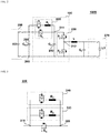
- FIG. 3 is a diagram illustrating an example of an initial charging circuit 220 including a first current control circuit 330 and a second current control circuit 340 according to an embodiment.
- the initial charging circuit 220 may include a first current control circuit 330 and a second current control circuit 340.
- the first current control circuit may include a third switch S p and a resistor R p
- the second current control circuit may include a fifth switch S p ' and a resistor R p '.
- the initial charging circuit 220 can perform rapid charging for the battery by supplying current through the first current control circuit 330 and/or the second current control circuit 340 according to the magnitude of the current capable of rapid charging.
- the resistor R p included in the first current control circuit 330 and the resistor R p ' included in the second current control circuit 340 may have different sizes.
- the initial charging circuit 220 may apply a voltage to the first node through at least one of the first current control circuit 330 and the second current control circuit 340, so that the magnitude of the current applied to the initial charging circuit 220 will not exceed the maximum magnitude of the current capable of rapid charging.
- the initial charging circuit 220 may supply a current of the first magnitude by turning on the third switch S p and turning off the fifth switch S p ', or may supply a current of the second magnitude By turning off the third switch S p and turning on the fifth switch S p ', or may supply a current of the third magnitude By turning on the third switch S p and turning on the fifth switch S p '.
- the third magnitude may be larger than the first magnitude and the second magnitude.
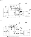
- FIG. 4 is a diagram illustrating an example of an operation of a DC-DC converter 100 when the voltage of the battery-side 270 is higher than the voltage of the inverter-side 280, according to an embodiment.
- the third switch S p When the voltage of the battery-side 270 is higher than the voltage of the inverter-side 280, a limited current may flow through the resistor R p by turning on the third switch S p .
- the third switch S p When sufficient current is applied from the battery-side 270 to the inverter-side 280 and the inverter-side capacitor 250 is charged by the voltage applied from the battery-side 270, the third switch S p is turned off and the fourth switch S b is turned on, so that the solar-linked system 1000 can be operated.
- the first switch S 1 , the second switch S 2 , the third switch S p , and the fourth switch S b may be turned off.
- the fourth switch S b may be firstly turned off and the third switch S p may be secondarily turned off, but the third switch S p and the fourth switch S b may be turned off almost simultaneously.
- the initial charging circuit 220 first turns off the fourth switch S b and secondarily turns off the third switch S p , so that spark generated by the current flowing through the initial charging circuit 220 may be reduced.
- FIG. 5 is a diagram illustrating an example of an operation of a DC-DC converter when the voltage of the battery-side 270 is lower than the voltage of the inverter-side 280, according to an embodiment.
- the first switch S 1 and the second switch S 2 may block current flowing to the battery-side 270.
- the third switch S p When the voltage of the battery-side 270 is lower than the voltage of the inverter-side 280, the third switch S p is turned off and the fourth switch S b is turned on, so that the solar-linked system is system 1000 can be operated.
- the first switch S 1 , the second switch S 2 , the third switch S p , and the fourth switch S b may be turned off.
- the fourth switch S b may be firstly turned off and the third switch S p may be secondarily turned off, but the third switch S p and the fourth switch S b may be turned off almost simultaneously.
- the initial charging circuit 220 first turns off the fourth switch S b and secondarily turns off the third switch S p , so that spark generated by the current flowing through the initial charging circuit 220 may be reduced.
- FIG. 6 is a diagram illustrating an example of a solar-linked system 1000 in which a diode is included in the initial charging circuit 610 according to an embodiment.
- a fifth switch 620 and a sixth switch 630 are disposed in series in the initial charging circuit 610.
- the diode 640 is disposed in parallel with the fifth switch 620 and the sixth switch 630.
- the diodes included in the fifth switch 620 and the sixth switch 630 may be disposed facing opposite directions. Accordingly, the fifth switch 620 and the sixth switch 630 may block both current flowing from left to right and current flowing from right to left.
- the diode 640 passes a current flowing from left to right, it can block a reverse current by blocking a current flowing from right to left.
- a first switch 651 and a second switch 652 are connected in series, and a third switch 653 and a fourth switch 654 may be connected in series.
- the first switch 651 and the second switch 652 may be connected in parallel with the third switch 653 and the fourth switch 654.
- the solar-linked system 1000 can operate only with the third switch 653 and the fourth switch 654, but when the output is greater than or equal to a predetermined value, the first switch 651 and the second switch 652 may be added in parallel.
- a first resistor 661 and a second resistor 662 may be connected to the battery-side.
- the output is greater than or equal to a predetermined value, the circuit is configured in parallel, so that a larger output can be accommodated.
- the fifth switch 620 and the sixth switch 630 may be different.
- the fifth switch 620 may have a specification of a low voltage
- the sixth switch 630 may have a specification of a high voltage.
- the fifth switch 620 may have a voltage specification higher than the voltage V F of the diode 640.
- the V F voltage may refer to a forward voltage capable of turning on the diode 640.
- the fifth switch 620 allows the current to flow from left to right only through the diode 640, so that the sixth switch 630 is not turned on in a situation where the current must flow from left to right.
- the fifth switch 620 may exclude a possibility that reverse current may occur according to the characteristics of the sixth switch 630.
- the above-described method can be written as a program that can be executed on a computer, and can be implemented in a general-purpose digital computer that operates the program using a computer-readable recording medium.
- the structure of the data used in the above-described method can be recorded on a computer-readable recording medium through various means.
- the computer-readable recording medium includes storage media such as magnetic storage media (for example, ROM, RAM, USB, floppy disk, hard disk, and the like), optical reading media (for example, CD-ROM, DVD, and the like).
Landscapes
- Engineering & Computer Science (AREA)
- Power Engineering (AREA)
- Charge And Discharge Circuits For Batteries Or The Like (AREA)
- Protection Of Static Devices (AREA)
- Dc-Dc Converters (AREA)
Abstract
Description
- In the present disclosure, in a solar-linked system, a DC-DC converter including a circuit for blocking current according to a control signal is disclosed.
- Recently, as awareness of environmental protection has been increased, interest in a method of generating electricity without discharging pollutants such as carbon dioxide has been emerged. In particular, in the case of a power generation system using solar light, the development and installation cost of the technology becomes cheaper powered by the technological advancement, and the supply is gradually expanding.
- In such a solar power generation system, a plurality of solar cells is assembled to form a plurality of photovoltaic modules. The DC power generated from the plurality of photovoltaic modules is converted to AC power through an inverter, and thus, it can be immediately used in industrial facilities.
- Meanwhile, in the case of solar power generation, a gap in power generation, during which sufficient power generation is not achieved due to night time when solar light is unavailable or changes in weather, occurs inevitably. Therefore, in order to compensate for such disadvantages, a solar power generation system is essentially equipped with a battery to enable stable power supply.
- However, there are many cases where a means for controlling the connection between the battery-side and the inverter-side is required when actually working or operating, and research related to this is being conducted.
- The present disclosure may disclose a DC-DC converter including a circuit for blocking current according to a control signal in a solar-linked system. Since the voltage on the battery-side is cut off at the inverter-side according to the control signal, the operator performing the installation and the like can easily work. In addition, when the voltage applied from the inverter-side is high, by blocking the current applied from the inverter according to the control signal the switch element in the DC-DC converter can be protected from the voltage applied from the inverter-side. The technical problem to be solved is not limited to the technical problems as described above, and various technical problems may be further included within a range that is obvious to a person skilled in the art.
- A DC-DC converter according to the first aspect comprises: an initial charging circuit that connects an inverter and a first node, and is used for charging a capacitor of the inverter-side; an intermediate capacitor connected between the first node and ground; and a switching circuit connected in parallel with the intermediate capacitor and composed of a first switch and a second switch connected in series, wherein the initial charging circuit applies a voltage to the first node according to a received control signal, so that the charging of the battery can be performed.
- In addition, the battery may be charged based on a voltage applied to a second node to which the first switch and the second switch are connected.
- In addition, the initial charging circuit may block a current flow according to a received control signal, so that a voltage applied to the inverter-side by the battery can be blocked.
- In addition, the initial charging circuit may include: a first current control circuit composed of a third switch and a resistor connected in series; and a fourth switch connected in parallel with the first current control circuit.
- In addition, the first current control circuit may perform rapid charging of the battery by supplying a current having a predetermined magnitude.
- In addition, the initial charging circuit further includes a second current control circuit, and the initial charging circuit may perform rapid charging of the battery by supplying current through the first current control circuit or the second current control circuit depending on the magnitude of current that can be rapidly charged.
- In addition, the resistor is a variable resistor, and the size of the variable resistor may be controlled according to the magnitude of a current capable of rapid charging.
- In addition, the first switch, the second switch, the third switch, and the fourth switch may include a field-effect transistor (FET).
- Further, the direction of the diodes of the third switch and the fourth switch may be a direction in which a current flowing from the first node to the inverter is blocked.
- In addition, the direction of the diode of the first switch may be a direction in which a current flowing from the first node to the second node is blocked.
- In addition, the direction of the diode of the second switch may be a direction in which a current flowing from the second node to the ground is blocked.
- In addition, the initial charging circuit, according to the passage of time, may apply a current in a state when the third switch is turned on at the first time point and the fourth switch is turned off, and apply current in a state when the third switch is turned on at the second time point and the fourth switch is turned on, and apply a current in a state when the third switch is turned off at the third time point and the fourth switch is turned on.
- A DC-DC converter according to the second aspect comprises: an initial charging circuit that connects the inverter and the first node, and is used for charging the capacitor of the inverter-side; and a switching circuit comprising a first switch and a second switch connected in series, and connected between the first node and a ground, wherein when a connection request signal is applied to the initial charging circuit, the initial charging circuit electrically connects the inverter-side and the first node, and wherein when a blocking request signal is applied to the initial charging circuit, the initial charging circuit electrically cuts off the inverter-side and the first node, and the voltage applied to the inverter-side can be blocked by a battery.
- In addition, the initial charging circuit may include: a first current control circuit composed of a third switch and a resistor connected in series; and a fourth switch connected in parallel with the first current control circuit.
- The DC-DC converter disclosed in the present disclosure may include a circuit that blocks current according to a control signal. Accordingly, since the voltage on the battery-side is cut off at the inverter-side according to the control signal, the operator performing the installation or the like can easily work. In addition, when the voltage applied from the inverter-side is high, the current applied from the inverter is blocked according to the control signal, so that the switching elements in the DC-DC converter can be protected from the voltage applied from the inverter-side.
-
-
FIG. 1 is a diagram illustrating a solar power generation system according to an embodiment. The solar-linked energy storage system may be an example of a solar power generation system. -
FIG. 2 is a block diagram illustrating in detail an example in which a DC-DC converter according to an embodiment is used in a solar-linked system. -
FIG. 3 is a diagram illustrating an example of an initial charging circuit including a first current control circuit and a second current control circuit according to an embodiment. -
FIG. 4 is a diagram illustrating an example of an operation of a DC-DC converter when the voltage of the battery-side is higher than the voltage of the inverter-side, according to an embodiment. -
FIG. 5 is a diagram illustrating an example of an operation of a DC-DC converter when the voltage of the battery-side is lower than the voltage of the inverter-side, according to an embodiment. - Hereinafter, embodiments of the present invention will be described in detail with reference to the accompanying drawings. However, the technical idea of the present invention is not limited to some embodiments to be described, but may be implemented in various forms, and if it is within the scope of the technical idea of the present invention, one or more of the components may be selected, combined, and substituted between the embodiments for use. In addition, terms (including technical and scientific terms) used in the embodiments of the present invention are generally understood by those of ordinary skill in the technical field to which the present invention belongs unless explicitly defined and described, and it can be interpreted as a meaning, and terms generally used, such as terms defined in a dictionary, may be interpreted in consideration of the meaning in the context of the related technology. In addition, terms used in the embodiments of the present invention are for describing the embodiments and are not intended to limit the present invention. In the present specification, the singular form may include the plural form unless specifically stated in the phrase, and when described as "at least one (or more than one) of A and B and C", it may contain one or more of all combinations that can be combined with A, B, and C. In addition, terms such as first, second, A, B, (a), (b), and the like may be used in describing the components of the embodiment of the present invention. These terms are only for distinguishing the component from other components, and are not limited to the nature, order, or order of the component by the term. And, when a component is described as being 'connected', 'coupled' or 'interconnected' to another component, the component is not only directly connected, coupled or interconnected to the other component, but may also include cases of being 'connected', 'coupled', or 'interconnected' due that another component between that other components. In addition, when it is described as being formed or disposed in the "top (upper side) or bottom (lower side)" of each component, the top (upper side) or bottom (lower side) not only includes a case when the two components are in direct contact with each other but also includes a case where one or more other components are formed or disposed between the two components. In addition, when expressed as "top (upper side) or bottom (lower side)", the meaning of not only an upward direction but also a downward direction based on one component may be included.
- Hereinafter, embodiments of the present invention will be described in detail with reference to the drawings.
-
FIG. 1 is a diagram illustrating a solar power generation system according to an embodiment. The solar-linked energy storage system may be an example of a solar power generation system. - As illustrated in
FIG. 1 , a solar power generation system may comprise asolar power supply 10, aninverter 20, abattery pack 30, and aload 50. - However, it can be understood by a person skilled in the art that general-purpose components other than the components illustrated in
FIG. 1 may be further included in the solar power generation system. For example, the solar power generation system may further include a power grid (GRID) 40. Or, according to another embodiment, it may be understood by a person skilled in the art that some of the components illustrated inFIG. 1 may be omitted. - The
solar power supply 10 according to an embodiment may be composed of a plurality of photovoltaic modules in which photovoltaic cells are assembled, and a photovoltaic cell formed by bonding a p-type semiconductor and an n-type semiconductor generates electricity with light. Specifically, when a light is irradiated on a photovoltaic cell, electrons and holes are generated therein. The generated charges are moved to the P and N poles, respectively, and by this action, a potential difference occurs between the P and N poles, and at this time, when a load is connected to the photovoltaic cell a current flows. Here, the photovoltaic cell refers to the smallest unit that generates electricity, and the photovoltaic cells are gathered to form a photovoltaic module, and the photovoltaic module may form an array connected in series/parallel to form asolar power supply 10. - In order to supply a power to the
power grid 40 or theload 50, theinverter 20 according to an embodiment may convert a direct current (DC) power generated by thesolar power supply 10 by the photoelectric effect to an alternating current (AC) power. Here, thepower grid 40 may refer to a grid for transmitting and distributing power produced by the solar power generation system. Meanwhile, the amount of power generated by thesolar power supply 10 is continuously changed by temporal factors such as sunrise and sunset, or external factors such as weather and the like. Therefore, theinverter 20 controls the voltage generated from thesolar power supply 10 to find the maximum power and supply it to thepower grid 40. At this time, when a case occurs in that the power for operating the inverter is lower than the output power of the inverter, theinverter 20 may consume the power of thepower grid 40 in reverse. Of course, in this case, the inverter may prevent power from being reversed by blocking the power flowing into thepower grid 40. Accordingly, various optimal control methods for extracting maximum power from thesolar power supply 10 are applied to the solar power generation system, so that the above-described operation of theinverter 20 can be performed more efficiently. - As a representative maximum power point (MPP) method of the
solar power supply 10, there are a perturbation and observation (PO) method, an incremental conductance (IC) control method, a constant voltage (CV) control method, and the like. Here, the PO method is a method of periodically measuring the voltage and current of thesolar power supply 10 to calculate power and then tracking the MPP using the power value. The IC control method is a method of measuring the voltage and current generated from thesolar power supply 10, so that the rate of change of the power with respect to the change of the operating point of the terminal voltage of the array becomes '0'. The CV control method is a method of controlling thesolar power supply 10 with a constant reference voltage regardless of the operating voltage or power of the array. According to each optimal control method, a power source input from thesolar power supply 10 to the inverter may operate as a voltage source or a current source. - The
load 50 according to an embodiment may refer to a product using an electricity type used in real life. For example, theinverter 20 may obtain AC power of a desired voltage and frequency through an appropriate conversion method, a switching element, or a control circuit, and supply electricity to home appliances in general homes or machinery products in industrial facilities. - In addition, in the case of solar power generation, a gap in power generation, during which sufficient power generation is not achieved due to night time when solar light is unavailable or changes in weather, occurs inevitably. Therefore, in order to compensate for such disadvantages, the solar power generation system is essentially equipped with a battery to enable stable power supply.
- A
battery pack 30 according to an embodiment may comprise at least one of a converter, a battery pack, a battery management system (BMS), and a battery control circuit. - The battery may be composed of a lithium ion battery or a nickel hydrogen battery, but is not necessarily limited to this configuration, and may refer to a battery that can be used semi-permanently through charging.
- DC-DC converter is a device that can convert DC power produced through the
solar power supply 10 into DC power suitable for a battery. In general, a power is converted in a way that a DC power is converted into an AC power and then the AC power is reverse converted to a DC power. - The battery management system (BMS) may provide a function of misuse protection of cells constituting the battery, balancing between unit cells, measuring the remaining amount of the charge (SOC), temperature maintenance management, or system monitoring function. Therefore, based on a sensor measuring the state of the cell and a function of receiving the measured value of the sensor and transmitting it to the control system of the applied product, it is possible to build and control circuits that generate an abnormal signal when the temperature and charging state and the like of the system exceed the set value and cut-off and open the power circuit between cells.
- Meanwhile, the
inverter 20 and thebattery pack 30 may further comprise a display device (not shown). For example, the user can check the supply and demand status of the power of the solar panel, reverse wiring, sleep mode operation, or the state of charge of the battery through the display device. Meanwhile, the display device may be a liquid crystal display, a thin film transistor-liquid crystal display, an organic light-emitting diode, a flexible display, a three dimensional (3D) display, an electrophoretic display, or the like. In addition, the display device may comprise two or more displays depending on the implementation type. In addition, when the touch pad of the display has a layer structure and is configured as a touch screen, the display may also be used as an input device in addition to an output device. - In addition, the
inverter 20 and thebattery pack 30 may communicate with each other through wired communication or wireless communication. For example, theinverter 20 and thebattery pack 30 may comprise a Wi-Fi chip, a Bluetooth chip, a wireless communication chip, an NFC chip, or the like. Of course, theinverter 20 and thebattery pack 30 may communicate with each other using various external devices using a Wi-Fi chip, a Bluetooth chip, a wireless communication chip, an NFC chip, and the like. The Wi-Fi chip and the Bluetooth chip can perform communication using a Wi-Fi method and a Bluetooth method, respectively. In the case of using a Wi-Fi chip or a Bluetooth chip, various types of connection information such as SSID, session key, and the like are first transmitted and received, and by using this, communication is connected and then various types of information may be transmitted and received. The wireless communication chip may perform communication according to various communication standards such as IEEE, ZigBee, 3rd Generation (3G), 3rd Generation Partnership Project (3GPP), Long Term Evolution (LTE), and the like. The NFC chip can operate in a Near Field Communication (NFC) method using a 13.56 MHz band among various RF-ID frequency bands such as 135 kHz, 13.56 MHz, 433 MHz, 860 to 960 MHz, 2.45 GHz, and the like. -
FIG. 2 is a block diagram illustrating in detail an example in which a DC-DC converter 100 according to an embodiment is used in a solar-linkedsystem 1000. - Referring to
FIG. 2 , a solar-linkedsystem 1000 according to an embodiment may comprise an inverter-side 280, a DC-DC converter 100, and a battery-side 270. In addition, the DC-DC converter 100 may include aninitial charging circuit 220, aswitching circuit 230 and anintermediate capacitor 240. In addition, theswitching circuit 230 may include a first switch S1 and a second switch S2 , and theinitial charging circuit 220 may include a first current control circuit including a third switch Sp and a resistor Rp , and a fourth switch S b. - A person skilled in the art can understand that other general-purpose components other than the components illustrated in
FIG. 2 may be further included in the solar-linkedsystem 1000 or the DC-DC converter 100. Or, according to another embodiment, it may be understood by a person skilled in the art that some of the components illustrated inFIG. 2 may be omitted. - As illustrated in
FIG. 2 , a solar-linkedsystem 1000 may be configured in a half-bridge form. When the solar-linkedsystem 1000 is configured in a half-bridge type, the voltage applied from the battery-side 270 can be directly transmitted to the inverter-side 280. Accordingly, theinitial charging circuit 220 may block the current passing through theinitial charging circuit 220 according to the control signal. When theinitial charging circuit 220 is cut off, since the voltage applied from the battery-side 270 can be prevented from being transmitted to the inverter-side 280, the operator's convenience during installation can be promoted. Especially, when the DC-DC converter 100 is manufactured as a battery integrated type, when a half bridge circuit is configured, the voltage of the battery is applied to the inverter-side 280, since theinitial charging circuit 220 is located in the middle, it is possible to prevent the voltage of the battery from being applied to the inverter-side 280, and the operator can easily work since the voltage is not induced in the inverter-side 280. - The
initial charging circuit 220 blocks a current flow according to a received control signal, so that a voltage applied to the inverter-side 280 by the battery can be blocked. - The
initial charging circuit 220 may connect or disconnect the right and left sides of theinitial charging circuit 220 according to a control signal. For example, theinitial charging circuit 220 is initially cut off and electrically separates the right and left sides of theinitial charging circuit 220, but when the installation is completed, the right side and the left side of theinitial charging circuit 220 can be connected. - The
initial charging circuit 220 may receive a control signal through communication, and the control signal may include a connection request signal and a blocking request signal. Specifically, when a connection request signal is applied to theinitial charging circuit 220, theinitial charging circuit 220 may electrically connect the inverter-side 280 and afirst node 211. When the inverter-side 280 and thefirst node 211 are electrically connected, charging of the battery can be performed based on the voltage applied to asecond node 212 to which the first switch S1 and the second switch S2 are connected. As another example, when theinitial charging circuit 220 is applied with a blocking request signal, theinitial charging circuit 220 cuts off the inverter-side 280 and thefirst node 211, so that the voltage applied to the inverter-side 280 by the battery can be cut off. - The
initial charging circuit 220 may include: a first current control circuit including a third switch Sp and a resistor Rp ; and a fourth switch Sb , wherein the first current control circuit and the fourth switch Sb may be connected in parallel. - The
initial charging circuit 220 may perform an initial charging function. For example, theinitial charging circuit 220 may charge the inverter-side capacitor 250 by using power source applied from the battery-side 270. In this case, theinitial charging circuit 220, according to the passage of time, may apply a current to thecapacitor 250 of the inverter-side in a state when the third switch Sp is turned on at the first time point and the fourth switch Sb is turned off, and apply current to thecapacitor 250 of the inverter-side in a state when the third switch Sp is turned on at the second time point and the fourth switch Sb is turned on, and apply a current to thecapacitor 250 of the inverter-side in a state when the third switch Sp is turned off at the third time point and the fourth switch Sb is turned on. - The
initial charging circuit 220 applies a voltage applied from the inverter-side 280 to thefirst node 211 according to a received control signal (e.g., a connection request signal), so that the charging of the battery can be performed by applying a voltage to the battery-side 270. - The
initial charging circuit 220 may perform rapid charging of the battery. For example, theinitial charging circuit 220 may turn on the fourth switch Sb to apply a voltage applied from the inverter-side 280 to thefirst node 211. However, when the voltage applied from the inverter-side 280 is directly connected to thefirst node 211, and if there is a risk of overcurrent flowing, theinitial charging circuit 220 may perform rapid charging of the battery by supplying a current of a predetermined magnitude through the first current control circuit. Since the first current control circuit contains the resistor Rp , when the fourth switch Sb is turned off and the third switch Sp is turned on, the voltage applied to the inverter-side 280 may not be directly applied to thefirst node 211. - The resistor Rp may be a variable resistor. In this case, the size of the variable resistor can be controlled according to the magnitude of the current capable of rapid charging. For example, when the
initial charging circuit 220 has a maximum current capable of rapid charging of 1 mA, the amount of current applied through theinitial charging circuit 220 can be maintained to be less than 1mA by controlling the size of the resistor R p. - The
intermediate capacitor 240 may be located between thefirst node 211 and theground 260, and theswitching circuit 230 may be connected to theintermediate capacitor 240 in parallel. The capacity of the inverter-side capacitor 250 may be greater than that of theintermediate capacitor 240. - The
switching circuit 230 may include a first switch S1 and a second switch S2 connected in series. The battery may be charged based on a voltage applied to thesecond node 212 to which the first switch S1 and the second switch S2 are connected. - A switch included in the DC-
DC converter 100 may be a field-effect transistor (FET). Specifically, the first switch S1 , the second switch S2 , the third switch Sp , and the fourth switch Sb may be implemented with FETs. - When the first switch S1 , the second switch S2 , the third switch Sp , and the fourth switch Sb are implemented with FETs, diodes included in each switch may be disposed in a predetermined direction. For example, the diode direction of the third switch Sp and the fourth switch Sb may be a direction in which a current flowing from the
first node 211 to the inverter-side 280 is blocked. As another example, the diode direction of the first switch S1 may be a direction that blocks a current flowing from thefirst node 211 to thesecond node 212. As another example, the diode direction of the second switch S2 may be a direction in which a current flowing from thesecond node 212 to theground 260 is blocked. - Since the
initial charging circuit 220 is included in the DC-DC converter 100, according to the control signal, the voltage of the battery-side 270 is cut off at the inverter-side 280, so that workers who install and the like can work easily. In addition, when the voltage applied from the inverter-side 280 is high, theinitial charging circuit 220 blocks the current applied from the inverter-side 280 according to the control signal, so that switches (e.g., the first switch S1 and the second switch S2 ) in the DC-DC converter 100 can be protected from a voltage applied from the inverter-side 280. -
FIG. 3 is a diagram illustrating an example of aninitial charging circuit 220 including a firstcurrent control circuit 330 and a secondcurrent control circuit 340 according to an embodiment. - The
initial charging circuit 220 according to an embodiment may include a firstcurrent control circuit 330 and a secondcurrent control circuit 340. The first current control circuit may include a third switch Sp and a resistor Rp , and the second current control circuit may include a fifth switch Sp ' and a resistor Rp '. - The
initial charging circuit 220 can perform rapid charging for the battery by supplying current through the firstcurrent control circuit 330 and/or the secondcurrent control circuit 340 according to the magnitude of the current capable of rapid charging. - The resistor Rp included in the first
current control circuit 330 and the resistor Rp ' included in the secondcurrent control circuit 340 may have different sizes. Theinitial charging circuit 220 may apply a voltage to the first node through at least one of the firstcurrent control circuit 330 and the secondcurrent control circuit 340, so that the magnitude of the current applied to theinitial charging circuit 220 will not exceed the maximum magnitude of the current capable of rapid charging. - For example, the
initial charging circuit 220 may supply a current of the first magnitude by turning on the third switch Sp and turning off the fifth switch Sp ', or may supply a current of the second magnitude By turning off the third switch Sp and turning on the fifth switch Sp ', or may supply a current of the third magnitude By turning on the third switch Sp and turning on the fifth switch Sp '. The third magnitude may be larger than the first magnitude and the second magnitude. -
FIG. 4 is a diagram illustrating an example of an operation of a DC-DC converter 100 when the voltage of the battery-side 270 is higher than the voltage of the inverter-side 280, according to an embodiment. - When the voltage of the battery-
side 270 is higher than the voltage of the inverter-side 280, a limited current may flow through the resistor Rp by turning on the third switch Sp . When sufficient current is applied from the battery-side 270 to the inverter-side 280 and the inverter-side capacitor 250 is charged by the voltage applied from the battery-side 270, the third switch Sp is turned off and the fourth switch Sb is turned on, so that the solar-linkedsystem 1000 can be operated. - When the operation of the solar-linked
system 1000 is stopped, the first switch S1 , the second switch S2 , the third switch Sp , and the fourth switch Sb may be turned off. When the operation of the solar-linkedsystem 1000 is stopped, the fourth switch Sb may be firstly turned off and the third switch Sp may be secondarily turned off, but the third switch Sp and the fourth switch Sb may be turned off almost simultaneously. For example, after the overall output of the solar-linkedsystem 1000 is reduced to less than a predetermined value, the third switch Sp and the fourth switch Sb may be turned off almost simultaneously. As another example, theinitial charging circuit 220 first turns off the fourth switch Sb and secondarily turns off the third switch Sp , so that spark generated by the current flowing through theinitial charging circuit 220 may be reduced. -
FIG. 5 is a diagram illustrating an example of an operation of a DC-DC converter when the voltage of the battery-side 270 is lower than the voltage of the inverter-side 280, according to an embodiment. - When the voltage of the battery-
side 270 is lower than the voltage of the inverter-side 280, the first switch S1 and the second switch S2 , as a semiconductor breaker, may block current flowing to the battery-side 270. - When the voltage of the battery-
side 270 is lower than the voltage of the inverter-side 280, the third switch Sp is turned off and the fourth switch Sb is turned on, so that the solar-linked system issystem 1000 can be operated. - When the operation of the solar-linked
system 1000 is stopped, the first switch S1 , the second switch S2 , the third switch Sp , and the fourth switch Sb may be turned off. When the operation of the solar-linkedsystem 1000 is stopped, the fourth switch Sb may be firstly turned off and the third switch Sp may be secondarily turned off, but the third switch Sp and the fourth switch Sb may be turned off almost simultaneously. For example, after the overall output of the solar-linkedsystem 1000 is reduced to less than a predetermined value, the third switch Sp and the fourth switch Sb may be turned off almost simultaneously. As another example, theinitial charging circuit 220 first turns off the fourth switch Sb and secondarily turns off the third switch Sp , so that spark generated by the current flowing through theinitial charging circuit 220 may be reduced. -
FIG. 6 is a diagram illustrating an example of a solar-linkedsystem 1000 in which a diode is included in theinitial charging circuit 610 according to an embodiment. - Referring to
FIG. 6 , afifth switch 620 and asixth switch 630 are disposed in series in theinitial charging circuit 610. In addition, thediode 640 is disposed in parallel with thefifth switch 620 and thesixth switch 630. Although thefifth switch 620 and thesixth switch 630 are disposed in series, the diodes included in thefifth switch 620 and thesixth switch 630 may be disposed facing opposite directions. Accordingly, thefifth switch 620 and thesixth switch 630 may block both current flowing from left to right and current flowing from right to left. - Further, although the
diode 640 passes a current flowing from left to right, it can block a reverse current by blocking a current flowing from right to left. - A
first switch 651 and asecond switch 652 are connected in series, and athird switch 653 and afourth switch 654 may be connected in series. In addition, thefirst switch 651 and thesecond switch 652 may be connected in parallel with thethird switch 653 and thefourth switch 654. The solar-linkedsystem 1000 can operate only with thethird switch 653 and thefourth switch 654, but when the output is greater than or equal to a predetermined value, thefirst switch 651 and thesecond switch 652 may be added in parallel. When thefirst switch 651 and thesecond switch 652 are added in parallel, afirst resistor 661 and asecond resistor 662 may be connected to the battery-side. When the output is greater than or equal to a predetermined value, the circuit is configured in parallel, so that a larger output can be accommodated. - Specifications of the
fifth switch 620 and thesixth switch 630 may be different. For example, thefifth switch 620 may have a specification of a low voltage, and thesixth switch 630 may have a specification of a high voltage. For example, thefifth switch 620 may have a voltage specification higher than the voltage VF of thediode 640. The VF voltage may refer to a forward voltage capable of turning on thediode 640. Thefifth switch 620 allows the current to flow from left to right only through thediode 640, so that thesixth switch 630 is not turned on in a situation where the current must flow from left to right. Thefifth switch 620 may exclude a possibility that reverse current may occur according to the characteristics of thesixth switch 630. - Meanwhile, the above-described method can be written as a program that can be executed on a computer, and can be implemented in a general-purpose digital computer that operates the program using a computer-readable recording medium. In addition, the structure of the data used in the above-described method can be recorded on a computer-readable recording medium through various means. The computer-readable recording medium includes storage media such as magnetic storage media (for example, ROM, RAM, USB, floppy disk, hard disk, and the like), optical reading media (for example, CD-ROM, DVD, and the like).
- It will be understood by a person of ordinary skill in the art related to the present embodiment that it may be implemented in a modified form within a scope not departing from the essential characteristics of the above description. Therefore, the disclosed methods should be considered from an explanatory point of view rather than a limiting point of view. The scope of the present invention is illustrated in the claims rather than the foregoing description, and all differences within the scope equivalent thereto should be construed as being included in the present invention.
Claims (14)
- A DC-DC converter comprising:an initial charging circuit for connecting an inverter and a first node, and being used for charging a capacitor of an inverter-side;an intermediate capacitor connected between the first node and ground; anda switching circuit connected in parallel with the intermediate capacitor and composed of a first switch and a second switch connected in series,wherein the initial charging circuit applies a voltage to the first node according to a received control signal, so executes a charging of the battery.
- The DC-DC converter according to claim 1, wherein the battery is charged based on a voltage applied to a second node to which the first switch and the second switch are connected.
- The DC-DC converter according to claim 1, wherein the initial charging circuit cuts off a current flow according to a received control signal, so cuts off a voltage applied to the inverter-side by the battery.
- The DC-DC converter according to claim 2, wherein the initial charging circuit includes:a first current control circuit composed of a third switch and a resistor connected in series; anda fourth switch connected in parallel with the first current control circuit.
- The DC-DC converter according to claim 4, wherein the first current control circuit executes a rapid charging of the battery by supplying a current having a predetermined magnitude.
- The DC-DC converter according to claim 5, wherein the initial charging circuit further includes a second current control circuit, and
wherein the initial charging circuit executes rapid charging of the battery by supplying current through the first current control circuit or the second current control circuit according to a magnitude of current that is capable of rapid charging. - The DC-DC converter according to claim 5, wherein the resistor is a variable resistor, and
wherein the size of the variable resistor is controlled according to a magnitude of current capable of rapid charging. - The DC-DC converter according to claim 4, wherein the first switch, the second switch, the third switch, and the fourth switch include a field-effect transistor (FET).
- The DC-DC converter according to claim 8, wherein the direction of the diodes of the third switch and the fourth switch is a direction in which a current flowing from the first node to the inverter is cut off.
- The DC-DC converter according to claim 8, wherein the direction of the diode of the first switch is a direction in which a current flowing from the first node to the second node is cut off.
- The DC-DC converter according to claim 8, wherein the direction of the diode of the second switch is a direction in which a current flowing from the second node to the ground is cut off.
- The DC-DC converter according to claim 1, wherein the initial charging circuit, according to the passage of time, applies a current in a state when the third switch is turned on at the first time point and the fourth switch is turned off, and applies current in a state when the third switch is turned on at the second time point and the fourth switch is turned on, and applies a current in a state when the third switch is turned off at the third time point and the fourth switch is turned on.
- A DC-DC converter comprising:an initial charging circuit for connecting an inverter and a first node, and being used for charging a capacitor of an inverter-side; anda switching circuit comprising a first switch and a second switch connected in series, and connected between the first node and a ground,wherein when a connection request signal is applied to the initial charging circuit, the initial charging circuit electrically connects the inverter-side and the first node, andwherein when a cut-off request signal is applied to the initial charging circuit, the initial charging circuit electrically cuts off the inverter-side and the first node, so cuts off a voltage applied to the inverter-side by a battery.
- The DC-DC converter according to claim 13, wherein the initial charging circuit includes:a first current control circuit composed of a third switch and a resistor connected in series; anda fourth switch connected in parallel with the first current control circuit.
Applications Claiming Priority (2)
| Application Number | Priority Date | Filing Date | Title |
|---|---|---|---|
| KR1020180098180A KR102699888B1 (en) | 2018-08-22 | 2018-08-22 | A DC-DC converter for photovoltaic linked system |
| PCT/KR2019/010592 WO2020040532A1 (en) | 2018-08-22 | 2019-08-20 | Dc-dc converter for solar-linked system |
Publications (2)
| Publication Number | Publication Date |
|---|---|
| EP3843254A1 true EP3843254A1 (en) | 2021-06-30 |
| EP3843254A4 EP3843254A4 (en) | 2022-07-27 |
Family
ID=69593230
Family Applications (1)
| Application Number | Title | Priority Date | Filing Date |
|---|---|---|---|
| EP19851842.5A Pending EP3843254A4 (en) | 2018-08-22 | 2019-08-20 | DC-DC CONVERTER FOR SOLAR LINKAGE SYSTEM |
Country Status (6)
| Country | Link |
|---|---|
| US (1) | US12047000B2 (en) |
| EP (1) | EP3843254A4 (en) |
| JP (1) | JP7536744B2 (en) |
| KR (1) | KR102699888B1 (en) |
| CN (1) | CN112585856B (en) |
| WO (1) | WO2020040532A1 (en) |
Families Citing this family (4)
| Publication number | Priority date | Publication date | Assignee | Title |
|---|---|---|---|---|
| KR102630252B1 (en) * | 2018-08-28 | 2024-01-29 | 엘지이노텍 주식회사 | A DC-DC converter for photovoltaic linked energy storage system and control method thereof |
| ES2983802T3 (en) * | 2021-07-29 | 2024-10-24 | Contemporary Amperex Technology Hong Kong Ltd | Charging/discharging apparatus, battery charging and discharging method and charging/discharging system |
| EP4546591A4 (en) * | 2022-06-23 | 2025-11-05 | Lg Innotek Co Ltd | POWER CONVERTER |
| CN116526531A (en) * | 2023-04-26 | 2023-08-01 | 华为数字能源技术有限公司 | Energy storage device and control method thereof |
Family Cites Families (31)
| Publication number | Priority date | Publication date | Assignee | Title |
|---|---|---|---|---|
| JP3095102B2 (en) | 1993-06-18 | 2000-10-03 | エヌイーシーワイヤレスネットワークス株式会社 | Inrush current prevention circuit |
| JPH08126339A (en) * | 1994-10-24 | 1996-05-17 | Miki Puurii Kk | Solar power system |
| JP4810775B2 (en) | 2001-08-03 | 2011-11-09 | 日本テキサス・インスツルメンツ株式会社 | DC-DC converter |
| JP2005073399A (en) | 2003-08-25 | 2005-03-17 | Toyota Motor Corp | Power supply device and automobile equipped with the same |
| JP2009247093A (en) | 2008-03-31 | 2009-10-22 | Kaga Electronics Co Ltd | Multiple-output dc-dc converter |
| US9755630B2 (en) | 2009-04-30 | 2017-09-05 | The United States of America as represented by the Secretary of the Government | Solid-state circuit breakers and related circuits |
| US8324822B2 (en) * | 2010-08-06 | 2012-12-04 | Ace Power International, Inc. | System and method for dimmable constant power light driver |
| EP2523333B1 (en) | 2011-05-11 | 2019-09-11 | Siemens Aktiengesellschaft | Method for operating of a frequency inverter with a regulated pre-charge |
| US8816625B2 (en) | 2011-10-27 | 2014-08-26 | Rockwell Automation Technologies, Inc. | Integrated regenerative AC drive with solid state precharging |
| US9373964B2 (en) * | 2012-05-16 | 2016-06-21 | General Electric Company | Optimized control of a power converter in response to load conditions |
| JP5538658B2 (en) | 2012-05-24 | 2014-07-02 | 三菱電機株式会社 | Power converter |
| TWI594656B (en) * | 2012-06-27 | 2017-08-01 | 登豐微電子股份有限公司 | Linear current regulator |
| CN102799557B (en) | 2012-07-16 | 2015-01-21 | 福建星网锐捷网络有限公司 | Hot plugging single board and method for measuring power of hot plugging single board |
| JP6162510B2 (en) | 2013-07-03 | 2017-07-12 | 株式会社ソニー・インタラクティブエンタテインメント | STEP-DOWN DC / DC CONVERTER, CONTROLLER AND CONTROL METHOD THEREOF, AND ELECTRONIC DEVICE USING THE SAME |
| JP5820021B1 (en) | 2014-06-13 | 2015-11-24 | ファナック株式会社 | Motor control device having charging resistance protection means |
| WO2016091281A1 (en) * | 2014-12-08 | 2016-06-16 | Siemens Aktiengesellschaft | Device for power limitation while switching a load, circuit arrangement, and method |
| JP6444204B2 (en) * | 2015-02-16 | 2018-12-26 | 三菱電機株式会社 | Power converter |
| JP2016174473A (en) * | 2015-03-17 | 2016-09-29 | 住友重機械工業株式会社 | Converter device |
| JP2015156795A (en) | 2015-04-20 | 2015-08-27 | 株式会社東芝 | Semiconductor switch circuit and power conversion device |
| JP2017017839A (en) | 2015-06-30 | 2017-01-19 | パナソニックIpマネジメント株式会社 | Semiconductor device |
| KR200491964Y1 (en) | 2015-07-20 | 2020-07-08 | 엘에스일렉트릭(주) | Battery disconnect unit |
| KR20170013671A (en) | 2015-07-28 | 2017-02-07 | 엘에스산전 주식회사 | A control apparatus for precharging of high voltage battery for electric vehicle |
| US10944392B2 (en) | 2015-11-17 | 2021-03-09 | Autonetworks Technologies, Ltd. | Switch circuit and power supply system |
| JP6477512B2 (en) | 2016-01-19 | 2019-03-06 | トヨタ自動車株式会社 | Fuel cell system |
| JP6699929B2 (en) | 2016-03-28 | 2020-05-27 | 住友重機械工業株式会社 | Inrush current reduction circuit and power converter |
| JP2017208979A (en) | 2016-05-20 | 2017-11-24 | 東芝キヤリア株式会社 | Power supply unit |
| DE102016219098B4 (en) * | 2016-09-30 | 2024-11-28 | Volkswagen Aktiengesellschaft | battery disconnect device |
| KR102657321B1 (en) | 2016-12-15 | 2024-04-12 | 현대자동차주식회사 | Charger |
| JP2019004593A (en) * | 2017-06-14 | 2019-01-10 | 本田技研工業株式会社 | Vehicle power supply |
| CN109287022B (en) * | 2017-07-21 | 2021-06-25 | 卡任特照明解决方案有限公司 | LED lamp |
| CN108123427A (en) | 2018-01-17 | 2018-06-05 | 华北电力大学 | A kind of inductive type bidirectional, dc current limiter topology |
-
2018
- 2018-08-22 KR KR1020180098180A patent/KR102699888B1/en active Active
-
2019
- 2019-08-20 US US17/266,394 patent/US12047000B2/en active Active
- 2019-08-20 WO PCT/KR2019/010592 patent/WO2020040532A1/en not_active Ceased
- 2019-08-20 CN CN201980054732.XA patent/CN112585856B/en active Active
- 2019-08-20 JP JP2021507776A patent/JP7536744B2/en active Active
- 2019-08-20 EP EP19851842.5A patent/EP3843254A4/en active Pending
Also Published As
| Publication number | Publication date |
|---|---|
| EP3843254A4 (en) | 2022-07-27 |
| US20210313888A1 (en) | 2021-10-07 |
| WO2020040532A1 (en) | 2020-02-27 |
| JP2022539927A (en) | 2022-09-14 |
| KR20200022265A (en) | 2020-03-03 |
| CN112585856B (en) | 2024-04-19 |
| JP7536744B2 (en) | 2024-08-20 |
| KR102699888B1 (en) | 2024-08-29 |
| US12047000B2 (en) | 2024-07-23 |
| CN112585856A (en) | 2021-03-30 |
Similar Documents
| Publication | Publication Date | Title |
|---|---|---|
| US12047000B2 (en) | DC-DC converter for solar-linked system | |
| US11979111B2 (en) | DC-DC converter for solar-related energy storage system, and control method thereof | |
| EP3284156B1 (en) | Battery module and method performed therein | |
| KR20060047861A (en) | Power supply and control method used for the power supply | |
| KR102284483B1 (en) | Battery Module and Driving Method Thereof | |
| US11418116B2 (en) | DC-DC converter for photovoltaic-linked energy storage system and control method therefor | |
| KR102597017B1 (en) | DC-DC Converter for Reverse Wiring Protection and Controlling Method Thereof | |
| US11626798B2 (en) | DC-DC converter for solar linked energy storage system and control method thereof | |
| US11916512B2 (en) | DC-DC converter for photovoltaic energy storage system and method for controlling same | |
| US11962232B2 (en) | DC-dC converter for solar power-linked energy storage system, and control method therefor | |
| KR102664413B1 (en) | Battery apparatus and power management method | |
| US11936337B2 (en) | DC-DC converter for solar-related energy storage system, and control method thereof | |
| RU2559025C2 (en) | Independent direct-current power supply system | |
| KR20240000307A (en) | Power converting apparatus | |
| KR20240000306A (en) | Power converting apparatus | |
| CN202872432U (en) | Household solar power generation device | |
| KR20240000305A (en) | Power converting apparatus |
Legal Events
| Date | Code | Title | Description |
|---|---|---|---|
| STAA | Information on the status of an ep patent application or granted ep patent |
Free format text: STATUS: THE INTERNATIONAL PUBLICATION HAS BEEN MADE |
|
| PUAI | Public reference made under article 153(3) epc to a published international application that has entered the european phase |
Free format text: ORIGINAL CODE: 0009012 |
|
| STAA | Information on the status of an ep patent application or granted ep patent |
Free format text: STATUS: REQUEST FOR EXAMINATION WAS MADE |
|
| 17P | Request for examination filed |
Effective date: 20210217 |
|
| AK | Designated contracting states |
Kind code of ref document: A1 Designated state(s): AL AT BE BG CH CY CZ DE DK EE ES FI FR GB GR HR HU IE IS IT LI LT LU LV MC MK MT NL NO PL PT RO RS SE SI SK SM TR |
|
| DAV | Request for validation of the european patent (deleted) | ||
| DAX | Request for extension of the european patent (deleted) | ||
| REG | Reference to a national code |
Ref country code: DE Ref legal event code: R079 Free format text: PREVIOUS MAIN CLASS: H02M0003156000 Ipc: H02M0001360000 |
|
| A4 | Supplementary search report drawn up and despatched |
Effective date: 20220628 |
|
| RIC1 | Information provided on ipc code assigned before grant |
Ipc: H02J 3/38 20060101ALI20220622BHEP Ipc: H02S 40/32 20140101ALI20220622BHEP Ipc: H02S 40/38 20140101ALI20220622BHEP Ipc: H02J 7/35 20060101ALI20220622BHEP Ipc: H02H 9/02 20060101ALI20220622BHEP Ipc: H02M 1/32 20070101ALI20220622BHEP Ipc: H02M 3/156 20060101ALI20220622BHEP Ipc: H02M 7/48 20070101ALI20220622BHEP Ipc: H02M 1/36 20070101AFI20220622BHEP |
|
| STAA | Information on the status of an ep patent application or granted ep patent |
Free format text: STATUS: EXAMINATION IS IN PROGRESS |
|
| 17Q | First examination report despatched |
Effective date: 20231106 |
|
| STAA | Information on the status of an ep patent application or granted ep patent |
Free format text: STATUS: THE APPLICATION HAS BEEN REFUSED |