EP3842897B1 - Niederspannungsteuerungssystem, niederspannungsschutzverfahren für eine elektronische vorrichtung und computerprogrammprodukt dafür - Google Patents
Niederspannungsteuerungssystem, niederspannungsschutzverfahren für eine elektronische vorrichtung und computerprogrammprodukt dafür Download PDFInfo
- Publication number
- EP3842897B1 EP3842897B1 EP20179708.1A EP20179708A EP3842897B1 EP 3842897 B1 EP3842897 B1 EP 3842897B1 EP 20179708 A EP20179708 A EP 20179708A EP 3842897 B1 EP3842897 B1 EP 3842897B1
- Authority
- EP
- European Patent Office
- Prior art keywords
- electronic device
- voltage
- low voltage
- control module
- protection method
- Prior art date
- Legal status (The legal status is an assumption and is not a legal conclusion. Google has not performed a legal analysis and makes no representation as to the accuracy of the status listed.)
- Active
Links
Images

Classifications
-
- G—PHYSICS
- G06—COMPUTING OR CALCULATING; COUNTING
- G06F—ELECTRIC DIGITAL DATA PROCESSING
- G06F1/00—Details not covered by groups G06F3/00 - G06F13/00 and G06F21/00
- G06F1/26—Power supply means, e.g. regulation thereof
- G06F1/30—Means for acting in the event of power-supply failure or interruption, e.g. power-supply fluctuations
Definitions
- the present invention relates to a low voltage control system for an electronic device, a low voltage protection method for an electronic device and a computer program product thereof; more particularly, the present invention relates to a low voltage control system for an electronic device, a low voltage protection method for an electronic device and a computer program product thereof capable of limiting a flash read/write permission by means of determining whether a current voltage of a power supply is lower than a threshold.
- the insufficiency is very likely to cause instantaneous interruption of the operation of the electronic device; if the software is accessing data of the flash memory at this time, such an abnormal interruption may result in incomplete hardware signals in the electronic device and thereby cause disorder in the memory data, which could make the electronic device boot or operate abnormally.
- a blinking light is used to remind the user to replace or recharge the battery.
- the blinking light itself will also accelerate the consumption of the battery power; moreover, the blinking light cannot solve the root cause of the problem of failure to access flash memory data due to the current voltage insufficiency of the electronic device, which still leaves room for improvement.
- the invention is directed to the subject-matter of the independent claims 1 and 3.
- Advantageous embodiments are set out in the dependent claims 2 and 4.
- a low voltage control system for an electronic device according to claim 1 is provided. Furthermore, according to the invention, a low voltage protection method for an electronic device according to claim 3 is provided. Moreover, according to the invention, a computer program product according to claim 5 is provided.
- the low voltage control system for an electronic device of the present invention is used in an electronic device.
- the electronic device comprises a power supply and a memory.
- the memory includes a plurality of access channels.
- the low voltage control system for an electronic device comprises a voltage detection module and a control module.
- the voltage detection module is used for detecting a current voltage of the power supply.
- the control module is electrically connected to the voltage detection module and is used for determining whether the current voltage is lower than a first voltage threshold. If the current voltage is lower than the first voltage threshold, the control module will cut off the plurality of access channels.
- the present invention further provides a low voltage protection method for an electronic device, which is used in an electronic device.
- the electronic device comprises a power supply and a memory.
- the low voltage protection method for an electronic device comprises the following steps: detecting a current voltage of the power supply; determining whether the current voltage is lower than a first voltage threshold; and if the current voltage is lower than the first voltage threshold, a control module cutting off a plurality of access channels.
- the present invention provides a computer program product, which is loaded into an electronic device and used for executing the low voltage protection method for an electronic device of the present invention.
- the present invention limits the flash read/write permission for an operation unit to access a memory by determining whether the current voltage of the power supply is lower than a first threshold or a second threshold so as to prevent data disorder caused by an unstable current voltage of the power supply. Furthermore, when the low voltage control system for an electronic device and the low voltage protection method for an electronic device of the present invention are used in a boot procedure of the electronic device, the present invention holds the electronic device in a half-started state and also limit the flash read/write permission of the operation unit to access the memory if the current voltage of the electronic device is insufficient to allow the electronic device to complete the normal boot procedure. As a result, the present invention prevents the electronic device from abnormal boot or boot failure due to data disorder caused by an unstable current voltage, thereby improving the deficiency of conventional techniques.
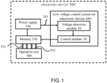
- FIG. 1 illustrates a schematic drawing of a low voltage control system for an electronic device according to the present invention.
- the low voltage control system for an electronic device 500 of the present invention is used in the electronic device 500.
- the electronic device 500 comprises a power supply 510, a memory 530 and an operation unit 540.
- the memory 530 includes a plurality of access channels 531 for the operation unit 540 to access data and operation commands in the memory 530.
- the electronic device 500 can be a desktop computer, a laptop computer, a tablet PC, a mobile device (such as a smart phone) or a wearable device (such as a smart watch);
- the power supply 510 is a lithium battery;
- the memory 530 is a flash memory;
- the access channels 531 includes a serial peripheral interface (SPI), an inter-integrated circuit (I 2 C) and a universal asynchronous receiver/transmitter (UART); and the operation unit 540 is a central processing unit (CPU).
- SPI serial peripheral interface
- I 2 C inter-integrated circuit
- UART universal asynchronous receiver/transmitter
- the operation unit 540 is a central processing unit (CPU).
- the low voltage control system for an electronic device 500 of the present invention comprises a voltage detection module 10 and a control module 20.
- the control module 20 is electrically connected to the voltage detection module 10.
- the voltage detection module 10 is used for detecting a current voltage 511 of the power supply 510.
- the control module 20 is used for determining whether the current voltage 511 is lower than a first voltage threshold. If the current voltage 511 is lower than the first voltage threshold, the control module 20 will cut off the plurality of access channels 531 so as to prevent the electronic device 500 from abnormal operations due to data disorder of the operation unit 540 caused by the low supplied voltage, thereby improving the operation stability of the electronic device 500.
- the first voltage threshold is 0.21 V.
- the control module 20 will determine that the electronic device 500 is in a low-supplied-voltage state; therefore, at this time the control module 20 will cut off the plurality of access channels 531.
- the voltage detection module 10 and the control module 20 can be disposed independently or combined together. Further, the embodiment disclosed herein is one of many preferred embodiments only. To avoid redundant descriptions, not all possible variations and combinations are disclosed in detail in this specification.
- the control module 20 not only determines whether the current voltage 511 is lower than the first voltage threshold but also determines whether the current voltage 511 is lower than a second voltage threshold, wherein the second voltage threshold is 2.1 V. If the current voltage 511 is lower than the second voltage threshold, the control module 20 will issue a warning signal.
- the warning signal causes a built-in LED light of the electronic device 500 to blink in order to remind the user to replace or recharge the battery of the electronic device 500.
- the first voltage threshold is one-tenth of the second voltage threshold.
- control module 20 will first utilize the LED light to remind the user to replace or recharge the battery when the current voltage 511 of the electronic device 500 is lower than the second voltage threshold. If the low voltage state has not changed, the control module 20 will continuously monitor whether the current voltage 511 continues to decline. Once the current voltage 511 is lower than the first voltage threshold, the control module 20 will cut off the plurality of access channels 531 to prevent the electronic device 500 from abnormal operations due to data disorder.
- the low voltage control system for an electronic device 500 of the present invention is used in a boot procedure of the electronic device 500.
- the control module 20 determines that the current voltage 511 is lower than the first voltage threshold, the control module 20 will cut off the plurality of access channels 531 and terminate the boot procedure of the electronic device 500 so as to hold the electronic device 500 in a half-started state, thereby preventing the electronic device 500 from abnormal boot or boot failure due to data disorder of the operation unit 540 caused by the unstable current voltage 511 of the electronic device 500.
- the half-started state means the state of only turning on the light signals or other auxiliary functions of the electronic device 500 without completing the boot procedure, which means the electronic device 500 does not fully execute the complete boot procedure.
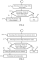
- FIG. 2 illustrates a flowchart of a low voltage protection method for an electronic device according to a first example not covered by the independent claims.
- the low voltage protection method for an electronic device of the present invention is used in an electronic device 500.
- the electronic device 500 comprises a power supply 510, a memory 530 and an operation unit 540.
- the electronic device 500 can be a desktop computer, a laptop computer, a tablet PC, a mobile device (such as a smart phone) or a wearable device (such as a smart watch);
- the power supply 510 is a lithium battery;
- the memory 530 is a flash memory;
- the access channels 531 include a serial peripheral interface (SPI), an inter-integrated circuit (I 2 C) and a universal asynchronous receiver/transmitter (UART); and the operation unit 540 is a central processing unit (CPU).
- the computer program product of the present invention can be loaded into the electronic device 500 so as to execute the steps of the first and second examples not covered by the independent claims and the embodiment of the low voltage protection method for an electronic device of the present invention.
- the first embodiment of the low voltage protection method for an electronic device of the present invention comprises steps S1 to S4. Please also refer to FIG. 1 for better understanding the steps as shown in FIG. 2 sequentially.
- Step S1 detecting a current voltage of the power supply.
- the voltage detection module 10 is used for detecting the current voltage 511 of the power supply 510.
- Step S2 determining whether the current voltage is lower than a first voltage threshold.
- the control module 20 will cut off the plurality of access channels 531 (step S3).
- the first voltage threshold 511 is 0.21 V. If the current voltage 511 is lower than 0.21 V, the control module 20 will determine that the electronic device 500 is in a low-supplied-voltage state; therefore, at this time the control module 20 will activate a low voltage protection mechanism for an electronic device in order to cut off the plurality of access channels 531, thereby preventing the electronic device 500 from abnormal operations due to data disorder of the operation unit 540 caused by the low current voltage 511, and thus improving the operation stability of the electronic device 500. In this embodiment, if the current voltage 511 is higher than the first voltage threshold, commands related to interfering with or interrupting a current operation mode of the electronic device 500 will not be executed.
- FIG. 3 illustrates a flowchart of the low voltage protection method for an electronic device according to a second example not covered by the independent claims.
- the second example not covered by the independent claims as shown in FIG. 3 , further comprises step S11a and step S31. Details of step S11a and step S31 will be further explained hereinafter.
- Step S11a executing a boot procedure of the electronic device.
- the low voltage protection method for an electronic device of the present invention is used in a boot procedure of the electronic device 500.
- the control module 20 will determine whether the current voltage 511 is lower than the first voltage threshold (step S1). If the control module 20 determines that the current voltage 511 is lower than the first voltage threshold (step S2), the control module 20 will cut off the plurality of access channels 531 (step S3) and terminate the boot procedure of the electronic device 500 (step S31) so as to hold the electronic device 500 in a half-started state, thereby preventing the electronic device 500 from abnormal boot or boot failure due to data disorder of the operation unit 540 caused by the unstable voltage of the electronic device 500.
- the half-started state means the state of only turning on the light signals or other auxiliary functions of the electronic device 500 without completing the boot procedure, which means the electronic device 500 does not fully execute the complete boot procedure.
- FIG. 4 illustrates a flowchart of the low voltage protection method for an electronic device according to an embodiment of the present invention.
- the embodiment as shown in FIG. 4 further comprises step S12 and step S13. Details of step S12 and step S13 will be further explained hereinafter.
- Step S12 determining whether the current voltage is lower than a second voltage threshold.
- the control module 20 When the electronic device 500 executes the boot procedure, the control module 20 not only determines whether the current voltage 511 is lower than the first voltage threshold but also determines whether the current voltage 511 is lower than a second voltage threshold, wherein the second voltage threshold is 2.1 V. If the current voltage 511 is lower than the second voltage threshold, the control module 20 will issue a warning signal.
- the warning signal causes a built-in LED light of the electronic device 500 to blink in order to remind the user to replace or recharge the battery of the electronic device 500.
- the first voltage threshold is one-tenth of the second voltage threshold.
- the control module 20 determines that the current voltage 511 of the electronic device 500 is lower than the second voltage threshold, the control module 20 will first utilize the LED light to remind the user to replace or recharge the battery of the electronic device 500.
- the control module 20 executes the boot procedure, if the current voltage 511 of the electronic device 500 is still lower than the second voltage threshold, the control module 20 will continuously monitor whether the current voltage 511 continues to decline. Once the current voltage 511 is lower than the first voltage threshold, the control module 20 will cut off the plurality of access channels 531 to prevent the electronic device 500 from abnormal operations due to data disorder.
- the present invention limits the flash read/write permission of the operation unit 540 to access the memory 530 by means of determining whether the current voltage 511 of the power supply 510 is lower than a first threshold or a second threshold so as to prevent data disorder caused by an unstable current voltage 511 of the power supply 510. Furthermore, when the low voltage control system for an electronic device and the low voltage protection method for an electronic device of the present invention are used in a boot procedure of the electronic device 500, the present invention holds the electronic device 500 in a half-started state and also limit the flash read/write permission of the operation unit 540 to access the memory 530 if the current voltage 511 of the electronic device 500 is insufficient to allow the electronic device 500 to complete the normal boot procedure. As a result, the present invention prevents the electronic device 500 from abnormal boot or boot failure due to data disorder caused by an unstable current voltage 511, thereby improving the deficiency of conventional techniques.
Landscapes
- Engineering & Computer Science (AREA)
- Theoretical Computer Science (AREA)
- Physics & Mathematics (AREA)
- General Engineering & Computer Science (AREA)
- General Physics & Mathematics (AREA)
- Power Sources (AREA)
Claims (5)
- Ein Niederspannung-Steuer-System für ein elektronisches Gerät (1), welches konfiguriert ist, um bei einem Bootvorgang eines elektronischen Geräts (500) verwendet zu werden, wobei das elektronische Gerät (500) eine Stromzufuhr (510) und einen Speicher (530) aufweist, und der Speicher (530) mehrere Zugriffskanäle (531) aufweist, wobei das Niederspannung-Steuer-System für ein elektronisches Gerät (1) aufweist:ein Spannung-Detektion-Modul (10), welches konfiguriert ist, um zum Detektieren einer aktuellen Spannung der Stromzufuhr (510) verwendet zu werden; undein Steuermodul (20), welches elektrisch mit dem Spannung-Detektion-Modul (10) verbunden ist, wobei das Steuermodul (20) konfiguriert ist, um zum Ermitteln verwendet zu werden, ob die aktuelle Spannung niedriger als ein erster Spannungsschwellenwert oder ein zweiter Spannungsschwellenwert ist, und wobei, falls die aktuelle Spannung niedriger als der erste Spannungsschwellenwert ist, das Steuermodul (20) konfiguriert sein wird, um die mehreren Zugriffskanäle (531) zu abzuschneiden und den Bootvorgang des elektronischen Geräts (500) abzubrechen, um das elektronische Gerät (500) in einem halbgestarteten Zustand zu halten; wobei, falls die aktuelle Spannung niedriger als der zweite Spannungsschwellenwert ist, das Steuermodul (10) konfiguriert sein wird, um ein Warnsignal auszugeben.
- Das Niederspannung-Steuer-System für ein elektronisches Gerät (1) nach Anspruch 1, wobei der erste Spannungsschwellenwert ein Zehntel des zweiten Spannungsschwellenwerts ist.
- Ein Niederspannung-Schutz-Verfahren für ein elektronisches Gerät (500), welches bei einem Bootvorgang des elektronischen Geräts (500) verwendet wird, wobei das elektronische Gerät (500) eine Stromzufuhr (510) und einen Speicher (530) aufweist, wobei der Speicher (530) mehrere Zugriffskanäle (531) aufweist, wobei das Niederspannung-Schutz-Verfahren für das elektronische Gerät (500) die folgenden Schritte aufweist:Detektieren, mittels eines Spannung-Detektion-Moduls (10), einer aktuellen Spannung der Stromzufuhr (510);ein Steuermodul (20), welches elektrisch mit dem Spannung-Detektion-Modul (10) verbunden ist,Ermitteln, ob die aktuelle Spannung niedriger als ein erster Spannungsschwellenwert oder ein zweiter Spannungsschwellenwert ist; und falls die aktuelle Spannung niedriger als der erste Spannungsschwellenwert istdas Steuermodul (10), welches die mehreren Zugangskanäle abschneidet und den Bootvorgang des elektronischen Geräts (500) abbricht, um das elektronische Gerät (500) in einem halbgestarteten Zustand zu halten;wobei, falls die aktuelle Spannung niedriger als der zweite Spannungsschwellenwert ist, das Steuermodul (10) ein Warnsignal ausgeben wird.
- Das Niederspannung-Schutz-Verfahren für ein elektronisches Gerät nach Anspruch 3, wobei der erste Spannungsschwellenwert ein Zehntel des zweiten Spannungsschwellenwertes ist.
- Ein Computerprogrammprodukt, welches in ein elektronisches Gerät (500) geladen und zum Ausführen des Niederspannung-Schutz-Verfahrens für ein elektronisches Gerät (500) nach Anspruch 3 verwendet wird.
Applications Claiming Priority (1)
| Application Number | Priority Date | Filing Date | Title |
|---|---|---|---|
| TW108147242A TWI740320B (zh) | 2019-12-23 | 2019-12-23 | 電子裝置低電壓控制系統、電子裝置低電壓保護方法及電腦程式產品 |
Publications (2)
| Publication Number | Publication Date |
|---|---|
| EP3842897A1 EP3842897A1 (de) | 2021-06-30 |
| EP3842897B1 true EP3842897B1 (de) | 2023-08-23 |
Family
ID=71094172
Family Applications (1)
| Application Number | Title | Priority Date | Filing Date |
|---|---|---|---|
| EP20179708.1A Active EP3842897B1 (de) | 2019-12-23 | 2020-06-12 | Niederspannungsteuerungssystem, niederspannungsschutzverfahren für eine elektronische vorrichtung und computerprogrammprodukt dafür |
Country Status (3)
| Country | Link |
|---|---|
| EP (1) | EP3842897B1 (de) |
| JP (1) | JP6977108B2 (de) |
| TW (1) | TWI740320B (de) |
Families Citing this family (3)
| Publication number | Priority date | Publication date | Assignee | Title |
|---|---|---|---|---|
| KR102872972B1 (ko) * | 2020-06-15 | 2025-10-17 | 현대자동차주식회사 | 트럭의 프런트캡 틸팅 스테이장치 |
| KR20230064674A (ko) | 2021-11-03 | 2023-05-11 | 삼성전자주식회사 | 저장 장치 및 그것의 동작 방법 |
| TWI825691B (zh) * | 2022-04-26 | 2023-12-11 | 正崴精密工業股份有限公司 | 低電壓保護方法 |
Family Cites Families (9)
| Publication number | Priority date | Publication date | Assignee | Title |
|---|---|---|---|---|
| JPH02310712A (ja) * | 1989-05-26 | 1990-12-26 | Mitsubishi Electric Corp | 半導体装置 |
| US5283792A (en) * | 1990-10-19 | 1994-02-01 | Benchmarq Microelectronics, Inc. | Power up/power down controller and power fail detector for processor |
| JPH09274059A (ja) * | 1996-04-04 | 1997-10-21 | Mitsubishi Electric Corp | 補助電池の電圧検知回路 |
| TW200410255A (en) * | 2002-12-10 | 2004-06-16 | Comax Semiconductor Inc | A memory device with power-saving mode and an electrics device with the memory device |
| JP2007133556A (ja) * | 2005-11-09 | 2007-05-31 | Dainippon Printing Co Ltd | Icカード及びicカードのプログラム |
| TWM435096U (en) * | 2011-10-28 | 2012-08-01 | Dynapack Internat Technology Corp | Energy device |
| CN104578324A (zh) * | 2015-02-04 | 2015-04-29 | 环旭电子股份有限公司 | 电池驱动装置 |
| CN108837271B (zh) * | 2018-03-26 | 2021-04-16 | Oppo广东移动通信有限公司 | 电子装置、提示信息的输出方法及相关产品 |
| TWI666875B (zh) * | 2018-12-25 | 2019-07-21 | 瑞昱半導體股份有限公司 | 連接電路及其連接方法 |
-
2019
- 2019-12-23 TW TW108147242A patent/TWI740320B/zh active
-
2020
- 2020-06-08 JP JP2020099044A patent/JP6977108B2/ja active Active
- 2020-06-12 EP EP20179708.1A patent/EP3842897B1/de active Active
Also Published As
| Publication number | Publication date |
|---|---|
| JP2021099773A (ja) | 2021-07-01 |
| TW202125158A (zh) | 2021-07-01 |
| TWI740320B (zh) | 2021-09-21 |
| EP3842897A1 (de) | 2021-06-30 |
| JP6977108B2 (ja) | 2021-12-08 |
Similar Documents
| Publication | Publication Date | Title |
|---|---|---|
| EP3652612B1 (de) | Verfahren und elektronische vorrichtung zur bereitstellung von moduswechsel und speichermedium dafür | |
| KR102216484B1 (ko) | 충전 제어 방법 및 그 장치 | |
| US8407495B2 (en) | Information processor and power supply method for an information processor | |
| US20130162198A1 (en) | Information processing apparatus and control method | |
| US20100199112A1 (en) | Information processing apparatus and power supply control method | |
| US10921870B2 (en) | System and method for hybrid power supply | |
| EP3842897A1 (de) | Niederspannungsteuerungssystem, niederspannungsschutzverfahren für eine elektronische vorrichtung und computerprogrammprodukt dafür | |
| KR20180103602A (ko) | 전자 장치의 배터리 관리 방법 및 그 장치 | |
| CN108845655A (zh) | 电子设备控制方法、装置、控制电路及电子设备 | |
| US11088557B2 (en) | Motherboard with a charging function | |
| US8782444B2 (en) | Circuit protection system and method for a circuit utilizing chip type power supply | |
| US11502504B2 (en) | Low voltage control system, low voltage protection method for an electronic device and a computer program product thereof | |
| CN112285597A (zh) | 显示面板的短路检测方法、装置 | |
| US9305452B2 (en) | Battery over-charge and over-discharge protection system and battery protection method able to release a protection state | |
| US8826056B2 (en) | Circuit protection system and method | |
| CN114442778A (zh) | 电源接入方法、电源切换方法与电子设备 | |
| US12032503B2 (en) | Electronic apparatus and signal switching method | |
| US11228194B2 (en) | Motherboard with a smart charging function | |
| US10644518B2 (en) | Battery power supply system and method | |
| CN113050779A (zh) | 电子装置低电压控制系统、电子装置低电压保护方法 | |
| CN107092340B (zh) | 一种功耗控制方法及电子设备 | |
| US20250321629A1 (en) | Electronic apparatus and control method for electronic apparatus | |
| KR102945443B1 (ko) | 전원 공급을 제어하는 방법 및 이를 이용한 전자 장치 | |
| KR20260038625A (ko) | 성능 테스트를 위한 저전력 환경을 유지하는 전자 시스템 및 방법 |
Legal Events
| Date | Code | Title | Description |
|---|---|---|---|
| PUAI | Public reference made under article 153(3) epc to a published international application that has entered the european phase |
Free format text: ORIGINAL CODE: 0009012 |
|
| STAA | Information on the status of an ep patent application or granted ep patent |
Free format text: STATUS: THE APPLICATION HAS BEEN PUBLISHED |
|
| AK | Designated contracting states |
Kind code of ref document: A1 Designated state(s): AL AT BE BG CH CY CZ DE DK EE ES FI FR GB GR HR HU IE IS IT LI LT LU LV MC MK MT NL NO PL PT RO RS SE SI SK SM TR |
|
| STAA | Information on the status of an ep patent application or granted ep patent |
Free format text: STATUS: REQUEST FOR EXAMINATION WAS MADE |
|
| 17P | Request for examination filed |
Effective date: 20211207 |
|
| RBV | Designated contracting states (corrected) |
Designated state(s): AL AT BE BG CH CY CZ DE DK EE ES FI FR GB GR HR HU IE IS IT LI LT LU LV MC MK MT NL NO PL PT RO RS SE SI SK SM TR |
|
| GRAP | Despatch of communication of intention to grant a patent |
Free format text: ORIGINAL CODE: EPIDOSNIGR1 |
|
| STAA | Information on the status of an ep patent application or granted ep patent |
Free format text: STATUS: GRANT OF PATENT IS INTENDED |
|
| INTG | Intention to grant announced |
Effective date: 20230313 |
|
| GRAS | Grant fee paid |
Free format text: ORIGINAL CODE: EPIDOSNIGR3 |
|
| GRAA | (expected) grant |
Free format text: ORIGINAL CODE: 0009210 |
|
| STAA | Information on the status of an ep patent application or granted ep patent |
Free format text: STATUS: THE PATENT HAS BEEN GRANTED |
|
| AK | Designated contracting states |
Kind code of ref document: B1 Designated state(s): AL AT BE BG CH CY CZ DE DK EE ES FI FR GB GR HR HU IE IS IT LI LT LU LV MC MK MT NL NO PL PT RO RS SE SI SK SM TR |
|
| REG | Reference to a national code |
Ref country code: GB Ref legal event code: FG4D |
|
| REG | Reference to a national code |
Ref country code: CH Ref legal event code: EP |
|
| REG | Reference to a national code |
Ref country code: DE Ref legal event code: R096 Ref document number: 602020016084 Country of ref document: DE |
|
| REG | Reference to a national code |
Ref country code: IE Ref legal event code: FG4D |
|
| REG | Reference to a national code |
Ref country code: LT Ref legal event code: MG9D |
|
| REG | Reference to a national code |
Ref country code: NL Ref legal event code: MP Effective date: 20230823 |
|
| REG | Reference to a national code |
Ref country code: AT Ref legal event code: MK05 Ref document number: 1603353 Country of ref document: AT Kind code of ref document: T Effective date: 20230823 |
|
| PG25 | Lapsed in a contracting state [announced via postgrant information from national office to epo] |
Ref country code: GR Free format text: LAPSE BECAUSE OF FAILURE TO SUBMIT A TRANSLATION OF THE DESCRIPTION OR TO PAY THE FEE WITHIN THE PRESCRIBED TIME-LIMIT Effective date: 20231124 |
|
| PG25 | Lapsed in a contracting state [announced via postgrant information from national office to epo] |
Ref country code: IS Free format text: LAPSE BECAUSE OF FAILURE TO SUBMIT A TRANSLATION OF THE DESCRIPTION OR TO PAY THE FEE WITHIN THE PRESCRIBED TIME-LIMIT Effective date: 20231223 |
|
| PG25 | Lapsed in a contracting state [announced via postgrant information from national office to epo] |
Ref country code: SE Free format text: LAPSE BECAUSE OF FAILURE TO SUBMIT A TRANSLATION OF THE DESCRIPTION OR TO PAY THE FEE WITHIN THE PRESCRIBED TIME-LIMIT Effective date: 20230823 Ref country code: RS Free format text: LAPSE BECAUSE OF FAILURE TO SUBMIT A TRANSLATION OF THE DESCRIPTION OR TO PAY THE FEE WITHIN THE PRESCRIBED TIME-LIMIT Effective date: 20230823 Ref country code: PT Free format text: LAPSE BECAUSE OF FAILURE TO SUBMIT A TRANSLATION OF THE DESCRIPTION OR TO PAY THE FEE WITHIN THE PRESCRIBED TIME-LIMIT Effective date: 20231226 Ref country code: NO Free format text: LAPSE BECAUSE OF FAILURE TO SUBMIT A TRANSLATION OF THE DESCRIPTION OR TO PAY THE FEE WITHIN THE PRESCRIBED TIME-LIMIT Effective date: 20231123 Ref country code: NL Free format text: LAPSE BECAUSE OF FAILURE TO SUBMIT A TRANSLATION OF THE DESCRIPTION OR TO PAY THE FEE WITHIN THE PRESCRIBED TIME-LIMIT Effective date: 20230823 Ref country code: LV Free format text: LAPSE BECAUSE OF FAILURE TO SUBMIT A TRANSLATION OF THE DESCRIPTION OR TO PAY THE FEE WITHIN THE PRESCRIBED TIME-LIMIT Effective date: 20230823 Ref country code: LT Free format text: LAPSE BECAUSE OF FAILURE TO SUBMIT A TRANSLATION OF THE DESCRIPTION OR TO PAY THE FEE WITHIN THE PRESCRIBED TIME-LIMIT Effective date: 20230823 Ref country code: IS Free format text: LAPSE BECAUSE OF FAILURE TO SUBMIT A TRANSLATION OF THE DESCRIPTION OR TO PAY THE FEE WITHIN THE PRESCRIBED TIME-LIMIT Effective date: 20231223 Ref country code: HR Free format text: LAPSE BECAUSE OF FAILURE TO SUBMIT A TRANSLATION OF THE DESCRIPTION OR TO PAY THE FEE WITHIN THE PRESCRIBED TIME-LIMIT Effective date: 20230823 Ref country code: GR Free format text: LAPSE BECAUSE OF FAILURE TO SUBMIT A TRANSLATION OF THE DESCRIPTION OR TO PAY THE FEE WITHIN THE PRESCRIBED TIME-LIMIT Effective date: 20231124 Ref country code: FI Free format text: LAPSE BECAUSE OF FAILURE TO SUBMIT A TRANSLATION OF THE DESCRIPTION OR TO PAY THE FEE WITHIN THE PRESCRIBED TIME-LIMIT Effective date: 20230823 Ref country code: AT Free format text: LAPSE BECAUSE OF FAILURE TO SUBMIT A TRANSLATION OF THE DESCRIPTION OR TO PAY THE FEE WITHIN THE PRESCRIBED TIME-LIMIT Effective date: 20230823 |
|
| PG25 | Lapsed in a contracting state [announced via postgrant information from national office to epo] |
Ref country code: PL Free format text: LAPSE BECAUSE OF FAILURE TO SUBMIT A TRANSLATION OF THE DESCRIPTION OR TO PAY THE FEE WITHIN THE PRESCRIBED TIME-LIMIT Effective date: 20230823 |
|
| PG25 | Lapsed in a contracting state [announced via postgrant information from national office to epo] |
Ref country code: ES Free format text: LAPSE BECAUSE OF FAILURE TO SUBMIT A TRANSLATION OF THE DESCRIPTION OR TO PAY THE FEE WITHIN THE PRESCRIBED TIME-LIMIT Effective date: 20230823 |
|
| PG25 | Lapsed in a contracting state [announced via postgrant information from national office to epo] |
Ref country code: SM Free format text: LAPSE BECAUSE OF FAILURE TO SUBMIT A TRANSLATION OF THE DESCRIPTION OR TO PAY THE FEE WITHIN THE PRESCRIBED TIME-LIMIT Effective date: 20230823 Ref country code: RO Free format text: LAPSE BECAUSE OF FAILURE TO SUBMIT A TRANSLATION OF THE DESCRIPTION OR TO PAY THE FEE WITHIN THE PRESCRIBED TIME-LIMIT Effective date: 20230823 Ref country code: ES Free format text: LAPSE BECAUSE OF FAILURE TO SUBMIT A TRANSLATION OF THE DESCRIPTION OR TO PAY THE FEE WITHIN THE PRESCRIBED TIME-LIMIT Effective date: 20230823 Ref country code: EE Free format text: LAPSE BECAUSE OF FAILURE TO SUBMIT A TRANSLATION OF THE DESCRIPTION OR TO PAY THE FEE WITHIN THE PRESCRIBED TIME-LIMIT Effective date: 20230823 Ref country code: DK Free format text: LAPSE BECAUSE OF FAILURE TO SUBMIT A TRANSLATION OF THE DESCRIPTION OR TO PAY THE FEE WITHIN THE PRESCRIBED TIME-LIMIT Effective date: 20230823 Ref country code: CZ Free format text: LAPSE BECAUSE OF FAILURE TO SUBMIT A TRANSLATION OF THE DESCRIPTION OR TO PAY THE FEE WITHIN THE PRESCRIBED TIME-LIMIT Effective date: 20230823 Ref country code: SK Free format text: LAPSE BECAUSE OF FAILURE TO SUBMIT A TRANSLATION OF THE DESCRIPTION OR TO PAY THE FEE WITHIN THE PRESCRIBED TIME-LIMIT Effective date: 20230823 |
|
| REG | Reference to a national code |
Ref country code: DE Ref legal event code: R097 Ref document number: 602020016084 Country of ref document: DE |
|
| PG25 | Lapsed in a contracting state [announced via postgrant information from national office to epo] |
Ref country code: IT Free format text: LAPSE BECAUSE OF FAILURE TO SUBMIT A TRANSLATION OF THE DESCRIPTION OR TO PAY THE FEE WITHIN THE PRESCRIBED TIME-LIMIT Effective date: 20230823 |
|
| PLBE | No opposition filed within time limit |
Free format text: ORIGINAL CODE: 0009261 |
|
| STAA | Information on the status of an ep patent application or granted ep patent |
Free format text: STATUS: NO OPPOSITION FILED WITHIN TIME LIMIT |
|
| 26N | No opposition filed |
Effective date: 20240524 |
|
| PG25 | Lapsed in a contracting state [announced via postgrant information from national office to epo] |
Ref country code: SI Free format text: LAPSE BECAUSE OF FAILURE TO SUBMIT A TRANSLATION OF THE DESCRIPTION OR TO PAY THE FEE WITHIN THE PRESCRIBED TIME-LIMIT Effective date: 20230823 |
|
| PG25 | Lapsed in a contracting state [announced via postgrant information from national office to epo] |
Ref country code: BG Free format text: LAPSE BECAUSE OF FAILURE TO SUBMIT A TRANSLATION OF THE DESCRIPTION OR TO PAY THE FEE WITHIN THE PRESCRIBED TIME-LIMIT Effective date: 20230823 |
|
| PG25 | Lapsed in a contracting state [announced via postgrant information from national office to epo] |
Ref country code: BG Free format text: LAPSE BECAUSE OF FAILURE TO SUBMIT A TRANSLATION OF THE DESCRIPTION OR TO PAY THE FEE WITHIN THE PRESCRIBED TIME-LIMIT Effective date: 20230823 |
|
| PG25 | Lapsed in a contracting state [announced via postgrant information from national office to epo] |
Ref country code: MC Free format text: LAPSE BECAUSE OF FAILURE TO SUBMIT A TRANSLATION OF THE DESCRIPTION OR TO PAY THE FEE WITHIN THE PRESCRIBED TIME-LIMIT Effective date: 20230823 |
|
| REG | Reference to a national code |
Ref country code: CH Ref legal event code: PL |
|
| PG25 | Lapsed in a contracting state [announced via postgrant information from national office to epo] |
Ref country code: LU Free format text: LAPSE BECAUSE OF NON-PAYMENT OF DUE FEES Effective date: 20240612 |
|
| PG25 | Lapsed in a contracting state [announced via postgrant information from national office to epo] |
Ref country code: IE Free format text: LAPSE BECAUSE OF NON-PAYMENT OF DUE FEES Effective date: 20240612 |
|
| PG25 | Lapsed in a contracting state [announced via postgrant information from national office to epo] |
Ref country code: BE Free format text: LAPSE BECAUSE OF NON-PAYMENT OF DUE FEES Effective date: 20240630 Ref country code: CH Free format text: LAPSE BECAUSE OF NON-PAYMENT OF DUE FEES Effective date: 20240630 |
|
| REG | Reference to a national code |
Ref country code: BE Ref legal event code: MM Effective date: 20240630 |
|
| PG25 | Lapsed in a contracting state [announced via postgrant information from national office to epo] |
Ref country code: CY Free format text: LAPSE BECAUSE OF FAILURE TO SUBMIT A TRANSLATION OF THE DESCRIPTION OR TO PAY THE FEE WITHIN THE PRESCRIBED TIME-LIMIT; INVALID AB INITIO Effective date: 20200612 |
|
| PG25 | Lapsed in a contracting state [announced via postgrant information from national office to epo] |
Ref country code: HU Free format text: LAPSE BECAUSE OF FAILURE TO SUBMIT A TRANSLATION OF THE DESCRIPTION OR TO PAY THE FEE WITHIN THE PRESCRIBED TIME-LIMIT; INVALID AB INITIO Effective date: 20200612 |
|
| PG25 | Lapsed in a contracting state [announced via postgrant information from national office to epo] |
Ref country code: TR Free format text: LAPSE BECAUSE OF FAILURE TO SUBMIT A TRANSLATION OF THE DESCRIPTION OR TO PAY THE FEE WITHIN THE PRESCRIBED TIME-LIMIT Effective date: 20230823 |
|
| PGFP | Annual fee paid to national office [announced via postgrant information from national office to epo] |
Ref country code: GB Payment date: 20260623 Year of fee payment: 7 |
|
| PGFP | Annual fee paid to national office [announced via postgrant information from national office to epo] |
Ref country code: DE Payment date: 20260521 Year of fee payment: 7 |
|
| PGFP | Annual fee paid to national office [announced via postgrant information from national office to epo] |
Ref country code: FR Payment date: 20260622 Year of fee payment: 7 |