EP3840021A1 - Improved device for drying semiconductor substrates - Google Patents
Improved device for drying semiconductor substrates Download PDFInfo
- Publication number
- EP3840021A1 EP3840021A1 EP19217346.6A EP19217346A EP3840021A1 EP 3840021 A1 EP3840021 A1 EP 3840021A1 EP 19217346 A EP19217346 A EP 19217346A EP 3840021 A1 EP3840021 A1 EP 3840021A1
- Authority
- EP
- European Patent Office
- Prior art keywords
- groove
- upper edge
- less
- wedge
- disc
- Prior art date
- Legal status (The legal status is an assumption and is not a legal conclusion. Google has not performed a legal analysis and makes no representation as to the accuracy of the status listed.)
- Granted
Links
Images
Classifications
-
- H—ELECTRICITY
- H10—SEMICONDUCTOR DEVICES; ELECTRIC SOLID-STATE DEVICES NOT OTHERWISE PROVIDED FOR
- H10P—GENERIC PROCESSES OR APPARATUS FOR THE MANUFACTURE OR TREATMENT OF DEVICES COVERED BY CLASS H10
- H10P72/00—Handling or holding of wafers, substrates or devices during manufacture or treatment thereof
- H10P72/04—Apparatus for manufacture or treatment
- H10P72/0402—Apparatus for fluid treatment
- H10P72/0406—Apparatus for fluid treatment for cleaning followed by drying, rinsing, stripping, blasting or the like
-
- H—ELECTRICITY
- H10—SEMICONDUCTOR DEVICES; ELECTRIC SOLID-STATE DEVICES NOT OTHERWISE PROVIDED FOR
- H10P—GENERIC PROCESSES OR APPARATUS FOR THE MANUFACTURE OR TREATMENT OF DEVICES COVERED BY CLASS H10
- H10P72/00—Handling or holding of wafers, substrates or devices during manufacture or treatment thereof
- H10P72/04—Apparatus for manufacture or treatment
- H10P72/0402—Apparatus for fluid treatment
- H10P72/0406—Apparatus for fluid treatment for cleaning followed by drying, rinsing, stripping, blasting or the like
- H10P72/0408—Apparatus for fluid treatment for cleaning followed by drying, rinsing, stripping, blasting or the like for drying
-
- H—ELECTRICITY
- H10—SEMICONDUCTOR DEVICES; ELECTRIC SOLID-STATE DEVICES NOT OTHERWISE PROVIDED FOR
- H10P—GENERIC PROCESSES OR APPARATUS FOR THE MANUFACTURE OR TREATMENT OF DEVICES COVERED BY CLASS H10
- H10P72/00—Handling or holding of wafers, substrates or devices during manufacture or treatment thereof
- H10P72/04—Apparatus for manufacture or treatment
- H10P72/0402—Apparatus for fluid treatment
- H10P72/0406—Apparatus for fluid treatment for cleaning followed by drying, rinsing, stripping, blasting or the like
- H10P72/0411—Apparatus for fluid treatment for cleaning followed by drying, rinsing, stripping, blasting or the like for wet cleaning or washing
- H10P72/0416—Apparatus for fluid treatment for cleaning followed by drying, rinsing, stripping, blasting or the like for wet cleaning or washing with the semiconductor substrates being dipped in baths or vessels
-
- H—ELECTRICITY
- H10—SEMICONDUCTOR DEVICES; ELECTRIC SOLID-STATE DEVICES NOT OTHERWISE PROVIDED FOR
- H10P—GENERIC PROCESSES OR APPARATUS FOR THE MANUFACTURE OR TREATMENT OF DEVICES COVERED BY CLASS H10
- H10P72/00—Handling or holding of wafers, substrates or devices during manufacture or treatment thereof
- H10P72/10—Handling or holding of wafers, substrates or devices during manufacture or treatment thereof using carriers specially adapted therefor, e.g. front opening unified pods [FOUP]
- H10P72/13—Horizontal boat type carrier whereby the substrates are vertically supported, e.g. comprising rod-shaped elements
Definitions
- the object of the invention is a device for use in drying disc-shaped semiconductor substrates.
- the invention relates to a device being used to treat semiconductor wafers, in which the latter are immersed for some time in a bath containing a liquid and are then taken therefrom so slowly that practically the whole quantity of liquid remains in the bath.
- a method of this kind may be used, for example, in the manufacture of electric circuits on all kinds of substrates, such as, for example, integrated circuits on semiconductor wafers (for example of silicon), drives for liquid crystal displays on transparent plates of glass or quartz or circuits on plates of synthetic material (circuit boards).
- the method may also be used in the manufacture of shadow masks for television picture tubes or in the manufacture of CD or VLP records.
- the substrates are immersed many times for some time in a bath containing a liquid, for example in galvanic baths for deposition of metals, in etching baths for etching patterns into metal layers or into semiconductor material, in development baths for developing exposed photo lacquer layers and in rinsing baths for cleaning the substrates. After treatment in the liquid baths, the substrates are taken from the liquid and are dried. The substrates can be taken from the liquid in that they are lifted or withdrawn from the liquid, but of course also in that the liquid is caused to flow out of the bath.
- the semiconductor wafer While being taken from the bath the semiconductor wafer reside on a device is used to hold the semiconductor wafer in place. During this process, the problem can arise that residues of liquid remain at the edge of the substrate. This can lead to unwanted particles on the edge of the substrate, which are later on effecting the quality of the semiconductor wafer.
- a device and a method to improve the quality of cleaning in respect to remaining particles of the semiconductor wafer is given in DE 10 2014 207 266 A1 . However, using this there are still particles left that reduce the quality of the semiconductor wafers.
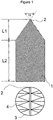
- Figure 1 shows a device (disc holder) for the present invention.
- the device for drying disc-shaped substrates comprises an elongated body (1), which tapers upwards to form a wedge having an angle ⁇ between two upper surfaces and the upper edge (2).
- the upper edge (2) is suitable for a disc-shaped substrate to be supported on.
- L1 is the height of the wedge and L2 is the length of the support part.
- the upper surface (3) comprises a groove (4) having an increasing groove depth with increasing distance from the upper edge (2).
- the groove is a triangular groove.
- the wedge opening angle ⁇ is larger than 30° and smaller than 90°, preferably more than 50° and less than 70°.
- the material used for the device comprises ceramic filled polyetheretherketone (CFM PEEK).
- the curvature radius of the upper edge is not less than 0.1mm and not more than 1mm.
- the two surface are hydrophobic.
- the maximum groove depth is not less than 1mm and not more than 5mm.
- an upper surface (3) comprises not less than 3 grooves (4).
- the groove (4) has a triangular shape.
- the opening angle of the triangular shape of a groove is not less than 80mm and not more than 100mm.
Landscapes
- Cleaning Or Drying Semiconductors (AREA)
- Container, Conveyance, Adherence, Positioning, Of Wafer (AREA)
Abstract
Description
- The object of the invention is a device for use in drying disc-shaped semiconductor substrates.
- The invention relates to a device being used to treat semiconductor wafers, in which the latter are immersed for some time in a bath containing a liquid and are then taken therefrom so slowly that practically the whole quantity of liquid remains in the bath.
- A method of this kind may be used, for example, in the manufacture of electric circuits on all kinds of substrates, such as, for example, integrated circuits on semiconductor wafers (for example of silicon), drives for liquid crystal displays on transparent plates of glass or quartz or circuits on plates of synthetic material (circuit boards). The method may also be used in the manufacture of shadow masks for television picture tubes or in the manufacture of CD or VLP records. In all these cases, the substrates are immersed many times for some time in a bath containing a liquid, for example in galvanic baths for deposition of metals, in etching baths for etching patterns into metal layers or into semiconductor material, in development baths for developing exposed photo lacquer layers and in rinsing baths for cleaning the substrates. After treatment in the liquid baths, the substrates are taken from the liquid and are dried. The substrates can be taken from the liquid in that they are lifted or withdrawn from the liquid, but of course also in that the liquid is caused to flow out of the bath.
- While being taken from the bath the semiconductor wafer reside on a device is used to hold the semiconductor wafer in place. During this process, the problem can arise that residues of liquid remain at the edge of the substrate. This can lead to unwanted particles on the edge of the substrate, which are later on effecting the quality of the semiconductor wafer.
- The physical effect utilized thereby are described in
CN1045539 A (EP 03 855 36 A1 ), as is an apparatus which is to some extent suitable for conduction of the method. - A device and a method to improve the quality of cleaning in respect to remaining particles of the semiconductor wafer is given in
DE 10 2014 207 266 A1 . However, using this there are still particles left that reduce the quality of the semiconductor wafers. - It is an object of the present invention to improve said device, and more particularly to show how the number of particles, which are found on the dried substrates, can be reduced by using this device.
-
Figure 1 shows a device (disc holder) for the present invention. - The device for drying disc-shaped substrates comprises an elongated body (1), which tapers upwards to form a wedge having an angle α between two upper surfaces and the upper edge (2). The upper edge (2) is suitable for a disc-shaped substrate to be supported on.
- L1 is the height of the wedge and L2 is the length of the support part.
- The upper surface (3) comprises a groove (4) having an increasing groove depth with increasing distance from the upper edge (2). Preferably, the groove is a triangular groove.
- Preferably, the wedge opening angle α is larger than 30° and smaller than 90°, preferably more than 50° and less than 70°.
- Preferably, the material used for the device comprises ceramic filled polyetheretherketone (CFM PEEK).
- Preferably, the curvature radius of the upper edge is not less than 0.1mm and not more than 1mm.
- Preferably, the two surface are hydrophobic.
- Preferably, the maximum groove depth is not less than 1mm and not more than 5mm.
- Preferably, an upper surface (3) comprises not less than 3 grooves (4).
- Preferably, the groove (4) has a triangular shape.
- Preferably, the opening angle of the triangular shape of a groove is not less than 80mm and not more than 100mm.
-
- L1
- Height of the wedge formed on top of the elongated body
- L2
- Height of the support part
- 1
- Elongated body
- 2
- Upper edge of the elongated body
- 3
- Upper Surface
- 4
- Chamfering diameter of the elongated body.
- α
- Opening angle of the wedge, angle between the upper two surfaces and an upper edge
Claims (8)
- Device for drying disc-shaped substrates comprising
an elongated body (1),
which tapers upwards to form a wedge having an angle α between two upper surfaces and the upper edge (2)
wherein the upper edge (2) is suitable for a disc-shaped substrate to be supported on, characterized in that
an upper surface (3) comprises a groove (4) having an increasing groove depth with increasing distance from the upper edge (2). - Device according to claim 1, characterized in that
the wedge opening angle α is larger than 30° and smaller than 90°, preferably larger than 50° and smaller than 70°. - Device according to claim 1 or claim 2, characterized in that
the material used for the device comprises ceramic filled polyetheretherketone (CFM PEEK). - Device according to claim 1 to claim 3, characterized in that
the curvature radius is not less than 0.1 mm and not more than 1mm. - Device according to claim 1 to claim 4, characterized in that
the maximum groove depth is not less than 1 mm and not more than 5mm. - Device according to claim 1 to claim 5, characterized in that
an upper surface (3) comprises not less than 3 grooves (4). - Device according to claim 1 to claim 6, characterized in that
the groove (4) has a triangular shape. - Device according to claim 7, characterized in that
the opening angle of the triangular shape of a groove is not less than 80° and not more than 100°.
Priority Applications (7)
| Application Number | Priority Date | Filing Date | Title |
|---|---|---|---|
| EP19217346.6A EP3840021B1 (en) | 2019-12-18 | 2019-12-18 | Improved device for drying semiconductor substrates |
| US17/784,117 US12598938B2 (en) | 2019-12-18 | 2020-11-27 | Device for drying semiconductor substrates |
| KR1020227021494A KR102721357B1 (en) | 2019-12-18 | 2020-11-27 | Improved device for drying semiconductor substrates |
| PCT/EP2020/083652 WO2021121901A1 (en) | 2019-12-18 | 2020-11-27 | Improved device for drying semiconductor substrates |
| CN202080088191.5A CN114830314A (en) | 2019-12-18 | 2020-11-27 | Improved apparatus for drying semiconductor substrates |
| JP2022537674A JP7451711B2 (en) | 2019-12-18 | 2020-11-27 | Improved equipment for drying semiconductor substrates |
| TW109143658A TWI738585B (en) | 2019-12-18 | 2020-12-10 | Improved device for drying semiconductor substrates |
Applications Claiming Priority (1)
| Application Number | Priority Date | Filing Date | Title |
|---|---|---|---|
| EP19217346.6A EP3840021B1 (en) | 2019-12-18 | 2019-12-18 | Improved device for drying semiconductor substrates |
Publications (2)
| Publication Number | Publication Date |
|---|---|
| EP3840021A1 true EP3840021A1 (en) | 2021-06-23 |
| EP3840021B1 EP3840021B1 (en) | 2022-10-19 |
Family
ID=69055637
Family Applications (1)
| Application Number | Title | Priority Date | Filing Date |
|---|---|---|---|
| EP19217346.6A Active EP3840021B1 (en) | 2019-12-18 | 2019-12-18 | Improved device for drying semiconductor substrates |
Country Status (7)
| Country | Link |
|---|---|
| US (1) | US12598938B2 (en) |
| EP (1) | EP3840021B1 (en) |
| JP (1) | JP7451711B2 (en) |
| KR (1) | KR102721357B1 (en) |
| CN (1) | CN114830314A (en) |
| TW (1) | TWI738585B (en) |
| WO (1) | WO2021121901A1 (en) |
Cited By (2)
| Publication number | Priority date | Publication date | Assignee | Title |
|---|---|---|---|---|
| EP4571823A1 (en) | 2023-12-11 | 2025-06-18 | Siltronic AG | Device and method for drying disc-shaped substrates |
| EP4600996A1 (en) | 2024-02-06 | 2025-08-13 | Siltronic AG | Device and method for drying disc-shaped substrates |
Citations (5)
| Publication number | Priority date | Publication date | Assignee | Title |
|---|---|---|---|---|
| EP0385536A1 (en) | 1989-02-27 | 1990-09-05 | Koninklijke Philips Electronics N.V. | Method and arrangement for drying substrates after treatment in a liquid |
| US20030145874A1 (en) * | 2002-02-06 | 2003-08-07 | Myland Lawrence J. | Capillary drying of substrates |
| US20070157951A1 (en) * | 2006-01-06 | 2007-07-12 | Micron Technology, Inc. | Systems and methods for processing microfeature workpieces |
| US20100078867A1 (en) * | 2008-09-29 | 2010-04-01 | Tokyo Electron Limited | Substrate processing apparatus |
| DE102014207266A1 (en) | 2014-04-15 | 2015-10-15 | Siltronic Ag | Method for drying disc-shaped substrates and disc holders for carrying out the method |
Family Cites Families (12)
| Publication number | Priority date | Publication date | Assignee | Title |
|---|---|---|---|---|
| US2158695A (en) * | 1938-10-21 | 1939-05-16 | Wooster Brush Co | Device for smoothing wallpaper and the like |
| JP3183098B2 (en) * | 1994-05-31 | 2001-07-03 | 大日本スクリーン製造株式会社 | Substrate holder for substrate processing equipment |
| DE19637875C2 (en) * | 1996-04-17 | 1999-07-22 | Steag Micro Tech Gmbh | Plant for the wet treatment of substrates |
| JP3714763B2 (en) * | 1997-03-31 | 2005-11-09 | 大日本スクリーン製造株式会社 | Substrate holding member and substrate processing apparatus using the same |
| JP3849846B2 (en) | 2001-05-21 | 2006-11-22 | 東京エレクトロン株式会社 | Rotating substrate processing apparatus and rotating substrate processing method |
| KR100678472B1 (en) * | 2005-01-25 | 2007-02-02 | 삼성전자주식회사 | Wafer Guide and Semiconductor Wafer Drying Apparatus Using the Same |
| WO2007047163A2 (en) * | 2005-10-04 | 2007-04-26 | Applied Materials, Inc. | Methods and apparatus for drying a substrate |
| JP4243289B2 (en) | 2006-08-28 | 2009-03-25 | 株式会社東芝 | Suction port and vacuum cleaner |
| JP2010275846A (en) | 2009-05-28 | 2010-12-09 | Noriko Hoshi | Wiper of convex mirror |
| US9064687B2 (en) | 2012-04-17 | 2015-06-23 | Dynamic Micro Systems | Substrate carrier having drip edge configurations |
| US9337066B2 (en) | 2013-11-05 | 2016-05-10 | Taiwan Semiconductor Manufacturing Co., Ltd. | Wafer cleaning module |
| CN107845590B (en) | 2017-11-02 | 2020-03-31 | 德淮半导体有限公司 | Cleaning device |
-
2019
- 2019-12-18 EP EP19217346.6A patent/EP3840021B1/en active Active
-
2020
- 2020-11-27 CN CN202080088191.5A patent/CN114830314A/en active Pending
- 2020-11-27 US US17/784,117 patent/US12598938B2/en active Active
- 2020-11-27 JP JP2022537674A patent/JP7451711B2/en active Active
- 2020-11-27 KR KR1020227021494A patent/KR102721357B1/en active Active
- 2020-11-27 WO PCT/EP2020/083652 patent/WO2021121901A1/en not_active Ceased
- 2020-12-10 TW TW109143658A patent/TWI738585B/en active
Patent Citations (6)
| Publication number | Priority date | Publication date | Assignee | Title |
|---|---|---|---|---|
| EP0385536A1 (en) | 1989-02-27 | 1990-09-05 | Koninklijke Philips Electronics N.V. | Method and arrangement for drying substrates after treatment in a liquid |
| CN1045539A (en) | 1989-02-27 | 1990-09-26 | 菲利浦光灯制造公司 | Substrate after liquid handling is carried out dry method and apparatus |
| US20030145874A1 (en) * | 2002-02-06 | 2003-08-07 | Myland Lawrence J. | Capillary drying of substrates |
| US20070157951A1 (en) * | 2006-01-06 | 2007-07-12 | Micron Technology, Inc. | Systems and methods for processing microfeature workpieces |
| US20100078867A1 (en) * | 2008-09-29 | 2010-04-01 | Tokyo Electron Limited | Substrate processing apparatus |
| DE102014207266A1 (en) | 2014-04-15 | 2015-10-15 | Siltronic Ag | Method for drying disc-shaped substrates and disc holders for carrying out the method |
Cited By (4)
| Publication number | Priority date | Publication date | Assignee | Title |
|---|---|---|---|---|
| EP4571823A1 (en) | 2023-12-11 | 2025-06-18 | Siltronic AG | Device and method for drying disc-shaped substrates |
| WO2025124890A1 (en) | 2023-12-11 | 2025-06-19 | Siltronic Ag | Device and method for drying disk-shaped substrates |
| EP4600996A1 (en) | 2024-02-06 | 2025-08-13 | Siltronic AG | Device and method for drying disc-shaped substrates |
| WO2025168307A1 (en) | 2024-02-06 | 2025-08-14 | Siltronic Ag | Device and method for drying disc-shaped substrates |
Also Published As
| Publication number | Publication date |
|---|---|
| EP3840021B1 (en) | 2022-10-19 |
| TW202125679A (en) | 2021-07-01 |
| JP7451711B2 (en) | 2024-03-18 |
| CN114830314A (en) | 2022-07-29 |
| KR20220106168A (en) | 2022-07-28 |
| WO2021121901A1 (en) | 2021-06-24 |
| KR102721357B1 (en) | 2024-10-23 |
| US20230016276A1 (en) | 2023-01-19 |
| JP2023507012A (en) | 2023-02-20 |
| US12598938B2 (en) | 2026-04-07 |
| TWI738585B (en) | 2021-09-01 |
Similar Documents
| Publication | Publication Date | Title |
|---|---|---|
| CN104246971B (en) | Method of manufacturing bonded wafers | |
| EP3840021B1 (en) | Improved device for drying semiconductor substrates | |
| CN101599451B (en) | Method for implementing edge chamfer on semiconductor substrate with insulating buried layer | |
| EP3840023B1 (en) | Improved device for drying semiconductor substrates | |
| EP3840022B1 (en) | Improved device for drying semiconductor substrates | |
| SG180053A1 (en) | Cleaning process and apparatus | |
| JP6005689B2 (en) | Stepper chuck for wafer or flat glass exposure equipment | |
| JP2008021686A (en) | Substrate holding tray | |
| KR102852298B1 (en) | Wafer cleaning apparatus | |
| JP4059016B2 (en) | Semiconductor substrate cleaning and drying method | |
| JP2005285798A (en) | Substrate holding mechanism, and substrate treatment apparatus and substrate treatment method using the same | |
| JPH0677201A (en) | Substrate cleaning method | |
| KR101684572B1 (en) | A method for recycling photomask | |
| KR20060092411A (en) | Wafer fixing jig, wafer coating apparatus and semiconductor device manufacturing method using the same | |
| KR20100074493A (en) | Dummy wafer and preparation method thereof | |
| CN107919299A (en) | Liquid level control system and method | |
| JPH06244267A (en) | Support jig for electronic components |
Legal Events
| Date | Code | Title | Description |
|---|---|---|---|
| PUAI | Public reference made under article 153(3) epc to a published international application that has entered the european phase |
Free format text: ORIGINAL CODE: 0009012 |
|
| STAA | Information on the status of an ep patent application or granted ep patent |
Free format text: STATUS: THE APPLICATION HAS BEEN PUBLISHED |
|
| AK | Designated contracting states |
Kind code of ref document: A1 Designated state(s): AL AT BE BG CH CY CZ DE DK EE ES FI FR GB GR HR HU IE IS IT LI LT LU LV MC MK MT NL NO PL PT RO RS SE SI SK SM TR |
|
| STAA | Information on the status of an ep patent application or granted ep patent |
Free format text: STATUS: REQUEST FOR EXAMINATION WAS MADE |
|
| 17P | Request for examination filed |
Effective date: 20210708 |
|
| RBV | Designated contracting states (corrected) |
Designated state(s): AL AT BE BG CH CY CZ DE DK EE ES FI FR GB GR HR HU IE IS IT LI LT LU LV MC MK MT NL NO PL PT RO RS SE SI SK SM TR |
|
| REG | Reference to a national code |
Ref country code: DE Ref legal event code: R079 Ref document number: 602019020773 Country of ref document: DE Free format text: PREVIOUS MAIN CLASS: H01L0021670000 Ipc: H01L0021673000 |
|
| GRAP | Despatch of communication of intention to grant a patent |
Free format text: ORIGINAL CODE: EPIDOSNIGR1 |
|
| STAA | Information on the status of an ep patent application or granted ep patent |
Free format text: STATUS: GRANT OF PATENT IS INTENDED |
|
| RIC1 | Information provided on ipc code assigned before grant |
Ipc: H01L 21/67 20060101ALI20211101BHEP Ipc: H01L 21/673 20060101AFI20211101BHEP |
|
| INTG | Intention to grant announced |
Effective date: 20211130 |
|
| GRAJ | Information related to disapproval of communication of intention to grant by the applicant or resumption of examination proceedings by the epo deleted |
Free format text: ORIGINAL CODE: EPIDOSDIGR1 |
|
| STAA | Information on the status of an ep patent application or granted ep patent |
Free format text: STATUS: REQUEST FOR EXAMINATION WAS MADE |
|
| INTC | Intention to grant announced (deleted) | ||
| GRAP | Despatch of communication of intention to grant a patent |
Free format text: ORIGINAL CODE: EPIDOSNIGR1 |
|
| STAA | Information on the status of an ep patent application or granted ep patent |
Free format text: STATUS: GRANT OF PATENT IS INTENDED |
|
| INTG | Intention to grant announced |
Effective date: 20220330 |
|
| GRAS | Grant fee paid |
Free format text: ORIGINAL CODE: EPIDOSNIGR3 |
|
| GRAA | (expected) grant |
Free format text: ORIGINAL CODE: 0009210 |
|
| STAA | Information on the status of an ep patent application or granted ep patent |
Free format text: STATUS: THE PATENT HAS BEEN GRANTED |
|
| AK | Designated contracting states |
Kind code of ref document: B1 Designated state(s): AL AT BE BG CH CY CZ DE DK EE ES FI FR GB GR HR HU IE IS IT LI LT LU LV MC MK MT NL NO PL PT RO RS SE SI SK SM TR |
|
| REG | Reference to a national code |
Ref country code: GB Ref legal event code: FG4D |
|
| REG | Reference to a national code |
Ref country code: CH Ref legal event code: EP |
|
| REG | Reference to a national code |
Ref country code: IE Ref legal event code: FG4D |
|
| REG | Reference to a national code |
Ref country code: DE Ref legal event code: R096 Ref document number: 602019020773 Country of ref document: DE |
|
| REG | Reference to a national code |
Ref country code: AT Ref legal event code: REF Ref document number: 1526095 Country of ref document: AT Kind code of ref document: T Effective date: 20221115 |
|
| REG | Reference to a national code |
Ref country code: LT Ref legal event code: MG9D |
|
| REG | Reference to a national code |
Ref country code: NL Ref legal event code: MP Effective date: 20221019 |
|
| REG | Reference to a national code |
Ref country code: AT Ref legal event code: MK05 Ref document number: 1526095 Country of ref document: AT Kind code of ref document: T Effective date: 20221019 |
|
| PG25 | Lapsed in a contracting state [announced via postgrant information from national office to epo] |
Ref country code: NL Free format text: LAPSE BECAUSE OF FAILURE TO SUBMIT A TRANSLATION OF THE DESCRIPTION OR TO PAY THE FEE WITHIN THE PRESCRIBED TIME-LIMIT Effective date: 20221019 |
|
| PG25 | Lapsed in a contracting state [announced via postgrant information from national office to epo] |
Ref country code: SE Free format text: LAPSE BECAUSE OF FAILURE TO SUBMIT A TRANSLATION OF THE DESCRIPTION OR TO PAY THE FEE WITHIN THE PRESCRIBED TIME-LIMIT Effective date: 20221019 Ref country code: PT Free format text: LAPSE BECAUSE OF FAILURE TO SUBMIT A TRANSLATION OF THE DESCRIPTION OR TO PAY THE FEE WITHIN THE PRESCRIBED TIME-LIMIT Effective date: 20230220 Ref country code: NO Free format text: LAPSE BECAUSE OF FAILURE TO SUBMIT A TRANSLATION OF THE DESCRIPTION OR TO PAY THE FEE WITHIN THE PRESCRIBED TIME-LIMIT Effective date: 20230119 Ref country code: LT Free format text: LAPSE BECAUSE OF FAILURE TO SUBMIT A TRANSLATION OF THE DESCRIPTION OR TO PAY THE FEE WITHIN THE PRESCRIBED TIME-LIMIT Effective date: 20221019 Ref country code: FI Free format text: LAPSE BECAUSE OF FAILURE TO SUBMIT A TRANSLATION OF THE DESCRIPTION OR TO PAY THE FEE WITHIN THE PRESCRIBED TIME-LIMIT Effective date: 20221019 Ref country code: ES Free format text: LAPSE BECAUSE OF FAILURE TO SUBMIT A TRANSLATION OF THE DESCRIPTION OR TO PAY THE FEE WITHIN THE PRESCRIBED TIME-LIMIT Effective date: 20221019 Ref country code: AT Free format text: LAPSE BECAUSE OF FAILURE TO SUBMIT A TRANSLATION OF THE DESCRIPTION OR TO PAY THE FEE WITHIN THE PRESCRIBED TIME-LIMIT Effective date: 20221019 |
|
| PG25 | Lapsed in a contracting state [announced via postgrant information from national office to epo] |
Ref country code: RS Free format text: LAPSE BECAUSE OF FAILURE TO SUBMIT A TRANSLATION OF THE DESCRIPTION OR TO PAY THE FEE WITHIN THE PRESCRIBED TIME-LIMIT Effective date: 20221019 Ref country code: PL Free format text: LAPSE BECAUSE OF FAILURE TO SUBMIT A TRANSLATION OF THE DESCRIPTION OR TO PAY THE FEE WITHIN THE PRESCRIBED TIME-LIMIT Effective date: 20221019 Ref country code: LV Free format text: LAPSE BECAUSE OF FAILURE TO SUBMIT A TRANSLATION OF THE DESCRIPTION OR TO PAY THE FEE WITHIN THE PRESCRIBED TIME-LIMIT Effective date: 20221019 Ref country code: IS Free format text: LAPSE BECAUSE OF FAILURE TO SUBMIT A TRANSLATION OF THE DESCRIPTION OR TO PAY THE FEE WITHIN THE PRESCRIBED TIME-LIMIT Effective date: 20230219 Ref country code: HR Free format text: LAPSE BECAUSE OF FAILURE TO SUBMIT A TRANSLATION OF THE DESCRIPTION OR TO PAY THE FEE WITHIN THE PRESCRIBED TIME-LIMIT Effective date: 20221019 Ref country code: GR Free format text: LAPSE BECAUSE OF FAILURE TO SUBMIT A TRANSLATION OF THE DESCRIPTION OR TO PAY THE FEE WITHIN THE PRESCRIBED TIME-LIMIT Effective date: 20230120 |
|
| REG | Reference to a national code |
Ref country code: DE Ref legal event code: R097 Ref document number: 602019020773 Country of ref document: DE |
|
| PG25 | Lapsed in a contracting state [announced via postgrant information from national office to epo] |
Ref country code: SM Free format text: LAPSE BECAUSE OF FAILURE TO SUBMIT A TRANSLATION OF THE DESCRIPTION OR TO PAY THE FEE WITHIN THE PRESCRIBED TIME-LIMIT Effective date: 20221019 Ref country code: RO Free format text: LAPSE BECAUSE OF FAILURE TO SUBMIT A TRANSLATION OF THE DESCRIPTION OR TO PAY THE FEE WITHIN THE PRESCRIBED TIME-LIMIT Effective date: 20221019 Ref country code: EE Free format text: LAPSE BECAUSE OF FAILURE TO SUBMIT A TRANSLATION OF THE DESCRIPTION OR TO PAY THE FEE WITHIN THE PRESCRIBED TIME-LIMIT Effective date: 20221019 Ref country code: DK Free format text: LAPSE BECAUSE OF FAILURE TO SUBMIT A TRANSLATION OF THE DESCRIPTION OR TO PAY THE FEE WITHIN THE PRESCRIBED TIME-LIMIT Effective date: 20221019 Ref country code: CZ Free format text: LAPSE BECAUSE OF FAILURE TO SUBMIT A TRANSLATION OF THE DESCRIPTION OR TO PAY THE FEE WITHIN THE PRESCRIBED TIME-LIMIT Effective date: 20221019 |
|
| REG | Reference to a national code |
Ref country code: CH Ref legal event code: PL |
|
| REG | Reference to a national code |
Ref country code: BE Ref legal event code: MM Effective date: 20221231 |
|
| PLBE | No opposition filed within time limit |
Free format text: ORIGINAL CODE: 0009261 |
|
| STAA | Information on the status of an ep patent application or granted ep patent |
Free format text: STATUS: NO OPPOSITION FILED WITHIN TIME LIMIT |
|
| PG25 | Lapsed in a contracting state [announced via postgrant information from national office to epo] |
Ref country code: SK Free format text: LAPSE BECAUSE OF FAILURE TO SUBMIT A TRANSLATION OF THE DESCRIPTION OR TO PAY THE FEE WITHIN THE PRESCRIBED TIME-LIMIT Effective date: 20221019 Ref country code: LU Free format text: LAPSE BECAUSE OF NON-PAYMENT OF DUE FEES Effective date: 20221218 Ref country code: AL Free format text: LAPSE BECAUSE OF FAILURE TO SUBMIT A TRANSLATION OF THE DESCRIPTION OR TO PAY THE FEE WITHIN THE PRESCRIBED TIME-LIMIT Effective date: 20221019 |
|
| 26N | No opposition filed |
Effective date: 20230720 |
|
| PG25 | Lapsed in a contracting state [announced via postgrant information from national office to epo] |
Ref country code: LI Free format text: LAPSE BECAUSE OF NON-PAYMENT OF DUE FEES Effective date: 20221231 Ref country code: IE Free format text: LAPSE BECAUSE OF NON-PAYMENT OF DUE FEES Effective date: 20221218 Ref country code: CH Free format text: LAPSE BECAUSE OF NON-PAYMENT OF DUE FEES Effective date: 20221231 |
|
| PG25 | Lapsed in a contracting state [announced via postgrant information from national office to epo] |
Ref country code: SI Free format text: LAPSE BECAUSE OF FAILURE TO SUBMIT A TRANSLATION OF THE DESCRIPTION OR TO PAY THE FEE WITHIN THE PRESCRIBED TIME-LIMIT Effective date: 20221019 Ref country code: FR Free format text: LAPSE BECAUSE OF NON-PAYMENT OF DUE FEES Effective date: 20221219 Ref country code: BE Free format text: LAPSE BECAUSE OF NON-PAYMENT OF DUE FEES Effective date: 20221231 |
|
| PG25 | Lapsed in a contracting state [announced via postgrant information from national office to epo] |
Ref country code: CY Free format text: LAPSE BECAUSE OF FAILURE TO SUBMIT A TRANSLATION OF THE DESCRIPTION OR TO PAY THE FEE WITHIN THE PRESCRIBED TIME-LIMIT Effective date: 20221019 |
|
| PG25 | Lapsed in a contracting state [announced via postgrant information from national office to epo] |
Ref country code: MK Free format text: LAPSE BECAUSE OF FAILURE TO SUBMIT A TRANSLATION OF THE DESCRIPTION OR TO PAY THE FEE WITHIN THE PRESCRIBED TIME-LIMIT Effective date: 20221019 Ref country code: IT Free format text: LAPSE BECAUSE OF FAILURE TO SUBMIT A TRANSLATION OF THE DESCRIPTION OR TO PAY THE FEE WITHIN THE PRESCRIBED TIME-LIMIT Effective date: 20221019 Ref country code: HU Free format text: LAPSE BECAUSE OF FAILURE TO SUBMIT A TRANSLATION OF THE DESCRIPTION OR TO PAY THE FEE WITHIN THE PRESCRIBED TIME-LIMIT; INVALID AB INITIO Effective date: 20191218 |
|
| PG25 | Lapsed in a contracting state [announced via postgrant information from national office to epo] |
Ref country code: MC Free format text: LAPSE BECAUSE OF FAILURE TO SUBMIT A TRANSLATION OF THE DESCRIPTION OR TO PAY THE FEE WITHIN THE PRESCRIBED TIME-LIMIT Effective date: 20221019 |
|
| PG25 | Lapsed in a contracting state [announced via postgrant information from national office to epo] |
Ref country code: MC Free format text: LAPSE BECAUSE OF FAILURE TO SUBMIT A TRANSLATION OF THE DESCRIPTION OR TO PAY THE FEE WITHIN THE PRESCRIBED TIME-LIMIT Effective date: 20221019 |
|
| PG25 | Lapsed in a contracting state [announced via postgrant information from national office to epo] |
Ref country code: BG Free format text: LAPSE BECAUSE OF FAILURE TO SUBMIT A TRANSLATION OF THE DESCRIPTION OR TO PAY THE FEE WITHIN THE PRESCRIBED TIME-LIMIT Effective date: 20221019 |
|
| GBPC | Gb: european patent ceased through non-payment of renewal fee |
Effective date: 20231218 |
|
| PG25 | Lapsed in a contracting state [announced via postgrant information from national office to epo] |
Ref country code: MT Free format text: LAPSE BECAUSE OF FAILURE TO SUBMIT A TRANSLATION OF THE DESCRIPTION OR TO PAY THE FEE WITHIN THE PRESCRIBED TIME-LIMIT Effective date: 20221019 |
|
| PG25 | Lapsed in a contracting state [announced via postgrant information from national office to epo] |
Ref country code: GB Free format text: LAPSE BECAUSE OF NON-PAYMENT OF DUE FEES Effective date: 20231218 |
|
| PG25 | Lapsed in a contracting state [announced via postgrant information from national office to epo] |
Ref country code: GB Free format text: LAPSE BECAUSE OF NON-PAYMENT OF DUE FEES Effective date: 20231218 |
|
| REG | Reference to a national code |
Ref country code: DE Ref legal event code: R079 Ref document number: 602019020773 Country of ref document: DE Free format text: PREVIOUS MAIN CLASS: H01L0021673000 Ipc: H10P0072100000 |
|
| PG25 | Lapsed in a contracting state [announced via postgrant information from national office to epo] |
Ref country code: TR Free format text: LAPSE BECAUSE OF FAILURE TO SUBMIT A TRANSLATION OF THE DESCRIPTION OR TO PAY THE FEE WITHIN THE PRESCRIBED TIME-LIMIT Effective date: 20221019 |
|
| PGFP | Annual fee paid to national office [announced via postgrant information from national office to epo] |
Ref country code: DE Payment date: 20251211 Year of fee payment: 7 |