EP3836207A1 - Semiconductor structure and method for manufacturing a semiconductor structure - Google Patents
Semiconductor structure and method for manufacturing a semiconductor structure Download PDFInfo
- Publication number
- EP3836207A1 EP3836207A1 EP19215556.2A EP19215556A EP3836207A1 EP 3836207 A1 EP3836207 A1 EP 3836207A1 EP 19215556 A EP19215556 A EP 19215556A EP 3836207 A1 EP3836207 A1 EP 3836207A1
- Authority
- EP
- European Patent Office
- Prior art keywords
- substrate
- radio frequency
- integrated circuit
- chip
- frequency integrated
- Prior art date
- Legal status (The legal status is an assumption and is not a legal conclusion. Google has not performed a legal analysis and makes no representation as to the accuracy of the status listed.)
- Granted
Links
Images




Classifications
-
- H—ELECTRICITY
- H10—SEMICONDUCTOR DEVICES; ELECTRIC SOLID-STATE DEVICES NOT OTHERWISE PROVIDED FOR
- H10W—GENERIC PACKAGES, INTERCONNECTIONS, CONNECTORS OR OTHER CONSTRUCTIONAL DETAILS OF DEVICES COVERED BY CLASS H10
- H10W20/00—Interconnections in chips, wafers or substrates
- H10W20/40—Interconnections external to wafers or substrates, e.g. back-end-of-line [BEOL] metallisations or vias connecting to gate electrodes
- H10W20/497—Inductive arrangements or effects of, or between, wiring layers
-
- H—ELECTRICITY
- H01—ELECTRIC ELEMENTS
- H01Q—ANTENNAS, i.e. RADIO AERIALS
- H01Q1/00—Details of, or arrangements associated with, antennas
- H01Q1/12—Supports; Mounting means
- H01Q1/22—Supports; Mounting means by structural association with other equipment or articles
- H01Q1/2283—Supports; Mounting means by structural association with other equipment or articles mounted in or on the surface of a semiconductor substrate as a chip-type antenna or integrated with other components into an IC package
-
- H—ELECTRICITY
- H01—ELECTRIC ELEMENTS
- H01Q—ANTENNAS, i.e. RADIO AERIALS
- H01Q13/00—Waveguide horns or mouths; Slot antennas; Leaky-waveguide antennas; Equivalent structures causing radiation along the transmission path of a guided wave
- H01Q13/10—Resonant slot antennas
-
- H—ELECTRICITY
- H01—ELECTRIC ELEMENTS
- H01Q—ANTENNAS, i.e. RADIO AERIALS
- H01Q19/00—Combinations of primary active antenna elements and units with secondary devices, e.g. with quasi-optical devices, for giving the antenna a desired directional characteristic
- H01Q19/06—Combinations of primary active antenna elements and units with secondary devices, e.g. with quasi-optical devices, for giving the antenna a desired directional characteristic using refracting or diffracting devices, e.g. lens
-
- H—ELECTRICITY
- H01—ELECTRIC ELEMENTS
- H01Q—ANTENNAS, i.e. RADIO AERIALS
- H01Q21/00—Antenna arrays or systems
- H01Q21/0087—Apparatus or processes specially adapted for manufacturing antenna arrays
- H01Q21/0093—Monolithic arrays
-
- H—ELECTRICITY
- H01—ELECTRIC ELEMENTS
- H01Q—ANTENNAS, i.e. RADIO AERIALS
- H01Q21/00—Antenna arrays or systems
- H01Q21/06—Arrays of individually energised antenna units similarly polarised and spaced apart
- H01Q21/061—Two dimensional planar arrays
- H01Q21/064—Two dimensional planar arrays using horn or slot aerials
-
- H—ELECTRICITY
- H10—SEMICONDUCTOR DEVICES; ELECTRIC SOLID-STATE DEVICES NOT OTHERWISE PROVIDED FOR
- H10W—GENERIC PACKAGES, INTERCONNECTIONS, CONNECTORS OR OTHER CONSTRUCTIONAL DETAILS OF DEVICES COVERED BY CLASS H10
- H10W20/00—Interconnections in chips, wafers or substrates
- H10W20/20—Interconnections within wafers or substrates, e.g. through-silicon vias [TSV]
-
- H—ELECTRICITY
- H10—SEMICONDUCTOR DEVICES; ELECTRIC SOLID-STATE DEVICES NOT OTHERWISE PROVIDED FOR
- H10W—GENERIC PACKAGES, INTERCONNECTIONS, CONNECTORS OR OTHER CONSTRUCTIONAL DETAILS OF DEVICES COVERED BY CLASS H10
- H10W44/00—Electrical arrangements for controlling or matching impedance
- H10W44/20—Electrical arrangements for controlling or matching impedance at high-frequency [HF] or radio frequency [RF]
-
- H—ELECTRICITY
- H10—SEMICONDUCTOR DEVICES; ELECTRIC SOLID-STATE DEVICES NOT OTHERWISE PROVIDED FOR
- H10W—GENERIC PACKAGES, INTERCONNECTIONS, CONNECTORS OR OTHER CONSTRUCTIONAL DETAILS OF DEVICES COVERED BY CLASS H10
- H10W44/00—Electrical arrangements for controlling or matching impedance
- H10W44/20—Electrical arrangements for controlling or matching impedance at high-frequency [HF] or radio frequency [RF]
- H10W44/241—Electrical arrangements for controlling or matching impedance at high-frequency [HF] or radio frequency [RF] for passive devices or passive elements
- H10W44/248—Electrical arrangements for controlling or matching impedance at high-frequency [HF] or radio frequency [RF] for passive devices or passive elements for antennas
-
- H—ELECTRICITY
- H10—SEMICONDUCTOR DEVICES; ELECTRIC SOLID-STATE DEVICES NOT OTHERWISE PROVIDED FOR
- H10W—GENERIC PACKAGES, INTERCONNECTIONS, CONNECTORS OR OTHER CONSTRUCTIONAL DETAILS OF DEVICES COVERED BY CLASS H10
- H10W70/00—Package substrates; Interposers; Redistribution layers [RDL]
- H10W70/60—Insulating or insulated package substrates; Interposers; Redistribution layers
- H10W70/67—Insulating or insulated package substrates; Interposers; Redistribution layers characterised by their insulating layers or insulating parts
- H10W70/68—Shapes or dispositions thereof
- H10W70/682—Shapes or dispositions thereof comprising holes having chips therein
-
- H—ELECTRICITY
- H10—SEMICONDUCTOR DEVICES; ELECTRIC SOLID-STATE DEVICES NOT OTHERWISE PROVIDED FOR
- H10W—GENERIC PACKAGES, INTERCONNECTIONS, CONNECTORS OR OTHER CONSTRUCTIONAL DETAILS OF DEVICES COVERED BY CLASS H10
- H10W72/00—Interconnections or connectors in packages
- H10W72/071—Connecting or disconnecting
- H10W72/0711—Apparatus therefor
- H10W72/07178—Means for aligning
-
- H—ELECTRICITY
- H10—SEMICONDUCTOR DEVICES; ELECTRIC SOLID-STATE DEVICES NOT OTHERWISE PROVIDED FOR
- H10W—GENERIC PACKAGES, INTERCONNECTIONS, CONNECTORS OR OTHER CONSTRUCTIONAL DETAILS OF DEVICES COVERED BY CLASS H10
- H10W72/00—Interconnections or connectors in packages
- H10W72/071—Connecting or disconnecting
- H10W72/072—Connecting or disconnecting of bump connectors
-
- H—ELECTRICITY
- H10—SEMICONDUCTOR DEVICES; ELECTRIC SOLID-STATE DEVICES NOT OTHERWISE PROVIDED FOR
- H10W—GENERIC PACKAGES, INTERCONNECTIONS, CONNECTORS OR OTHER CONSTRUCTIONAL DETAILS OF DEVICES COVERED BY CLASS H10
- H10W72/00—Interconnections or connectors in packages
- H10W72/071—Connecting or disconnecting
- H10W72/073—Connecting or disconnecting of die-attach connectors
-
- H—ELECTRICITY
- H10—SEMICONDUCTOR DEVICES; ELECTRIC SOLID-STATE DEVICES NOT OTHERWISE PROVIDED FOR
- H10W—GENERIC PACKAGES, INTERCONNECTIONS, CONNECTORS OR OTHER CONSTRUCTIONAL DETAILS OF DEVICES COVERED BY CLASS H10
- H10W72/00—Interconnections or connectors in packages
- H10W72/071—Connecting or disconnecting
- H10W72/075—Connecting or disconnecting of bond wires
-
- H—ELECTRICITY
- H10—SEMICONDUCTOR DEVICES; ELECTRIC SOLID-STATE DEVICES NOT OTHERWISE PROVIDED FOR
- H10W—GENERIC PACKAGES, INTERCONNECTIONS, CONNECTORS OR OTHER CONSTRUCTIONAL DETAILS OF DEVICES COVERED BY CLASS H10
- H10W72/00—Interconnections or connectors in packages
- H10W72/20—Bump connectors, e.g. solder bumps or copper pillars; Dummy bumps; Thermal bumps
- H10W72/241—Dispositions, e.g. layouts
-
- H—ELECTRICITY
- H10—SEMICONDUCTOR DEVICES; ELECTRIC SOLID-STATE DEVICES NOT OTHERWISE PROVIDED FOR
- H10W—GENERIC PACKAGES, INTERCONNECTIONS, CONNECTORS OR OTHER CONSTRUCTIONAL DETAILS OF DEVICES COVERED BY CLASS H10
- H10W72/00—Interconnections or connectors in packages
- H10W72/20—Bump connectors, e.g. solder bumps or copper pillars; Dummy bumps; Thermal bumps
- H10W72/251—Materials
- H10W72/252—Materials comprising solid metals or solid metalloids, e.g. PbSn, Ag or Cu
-
- H—ELECTRICITY
- H10—SEMICONDUCTOR DEVICES; ELECTRIC SOLID-STATE DEVICES NOT OTHERWISE PROVIDED FOR
- H10W—GENERIC PACKAGES, INTERCONNECTIONS, CONNECTORS OR OTHER CONSTRUCTIONAL DETAILS OF DEVICES COVERED BY CLASS H10
- H10W72/00—Interconnections or connectors in packages
- H10W72/20—Bump connectors, e.g. solder bumps or copper pillars; Dummy bumps; Thermal bumps
- H10W72/29—Bond pads specially adapted therefor
-
- H—ELECTRICITY
- H10—SEMICONDUCTOR DEVICES; ELECTRIC SOLID-STATE DEVICES NOT OTHERWISE PROVIDED FOR
- H10W—GENERIC PACKAGES, INTERCONNECTIONS, CONNECTORS OR OTHER CONSTRUCTIONAL DETAILS OF DEVICES COVERED BY CLASS H10
- H10W72/00—Interconnections or connectors in packages
- H10W72/50—Bond wires
- H10W72/551—Materials of bond wires
-
- H—ELECTRICITY
- H10—SEMICONDUCTOR DEVICES; ELECTRIC SOLID-STATE DEVICES NOT OTHERWISE PROVIDED FOR
- H10W—GENERIC PACKAGES, INTERCONNECTIONS, CONNECTORS OR OTHER CONSTRUCTIONAL DETAILS OF DEVICES COVERED BY CLASS H10
- H10W72/00—Interconnections or connectors in packages
- H10W72/50—Bond wires
- H10W72/59—Bond pads specially adapted therefor
-
- H—ELECTRICITY
- H10—SEMICONDUCTOR DEVICES; ELECTRIC SOLID-STATE DEVICES NOT OTHERWISE PROVIDED FOR
- H10W—GENERIC PACKAGES, INTERCONNECTIONS, CONNECTORS OR OTHER CONSTRUCTIONAL DETAILS OF DEVICES COVERED BY CLASS H10
- H10W72/00—Interconnections or connectors in packages
- H10W72/851—Dispositions of multiple connectors or interconnections
- H10W72/853—On the same surface
- H10W72/859—Bump connectors and bond wires
-
- H—ELECTRICITY
- H10—SEMICONDUCTOR DEVICES; ELECTRIC SOLID-STATE DEVICES NOT OTHERWISE PROVIDED FOR
- H10W—GENERIC PACKAGES, INTERCONNECTIONS, CONNECTORS OR OTHER CONSTRUCTIONAL DETAILS OF DEVICES COVERED BY CLASS H10
- H10W72/00—Interconnections or connectors in packages
- H10W72/851—Dispositions of multiple connectors or interconnections
- H10W72/874—On different surfaces
- H10W72/877—Bump connectors and die-attach connectors
-
- H—ELECTRICITY
- H10—SEMICONDUCTOR DEVICES; ELECTRIC SOLID-STATE DEVICES NOT OTHERWISE PROVIDED FOR
- H10W—GENERIC PACKAGES, INTERCONNECTIONS, CONNECTORS OR OTHER CONSTRUCTIONAL DETAILS OF DEVICES COVERED BY CLASS H10
- H10W72/00—Interconnections or connectors in packages
- H10W72/851—Dispositions of multiple connectors or interconnections
- H10W72/874—On different surfaces
- H10W72/884—Die-attach connectors and bond wires
-
- H—ELECTRICITY
- H10—SEMICONDUCTOR DEVICES; ELECTRIC SOLID-STATE DEVICES NOT OTHERWISE PROVIDED FOR
- H10W—GENERIC PACKAGES, INTERCONNECTIONS, CONNECTORS OR OTHER CONSTRUCTIONAL DETAILS OF DEVICES COVERED BY CLASS H10
- H10W72/00—Interconnections or connectors in packages
- H10W72/90—Bond pads, in general
- H10W72/931—Shapes of bond pads
- H10W72/932—Plan-view shape, i.e. in top view
-
- H—ELECTRICITY
- H10—SEMICONDUCTOR DEVICES; ELECTRIC SOLID-STATE DEVICES NOT OTHERWISE PROVIDED FOR
- H10W—GENERIC PACKAGES, INTERCONNECTIONS, CONNECTORS OR OTHER CONSTRUCTIONAL DETAILS OF DEVICES COVERED BY CLASS H10
- H10W72/00—Interconnections or connectors in packages
- H10W72/90—Bond pads, in general
- H10W72/941—Dispositions of bond pads
- H10W72/944—Dispositions of multiple bond pads
- H10W72/9445—Top-view layouts, e.g. mirror arrays
-
- H—ELECTRICITY
- H10—SEMICONDUCTOR DEVICES; ELECTRIC SOLID-STATE DEVICES NOT OTHERWISE PROVIDED FOR
- H10W—GENERIC PACKAGES, INTERCONNECTIONS, CONNECTORS OR OTHER CONSTRUCTIONAL DETAILS OF DEVICES COVERED BY CLASS H10
- H10W90/00—Package configurations
-
- H—ELECTRICITY
- H10—SEMICONDUCTOR DEVICES; ELECTRIC SOLID-STATE DEVICES NOT OTHERWISE PROVIDED FOR
- H10W—GENERIC PACKAGES, INTERCONNECTIONS, CONNECTORS OR OTHER CONSTRUCTIONAL DETAILS OF DEVICES COVERED BY CLASS H10
- H10W90/00—Package configurations
- H10W90/20—Configurations of stacked chips
- H10W90/28—Configurations of stacked chips the stacked chips having different sizes, e.g. chip stacks having a pyramidal shape
-
- H—ELECTRICITY
- H10—SEMICONDUCTOR DEVICES; ELECTRIC SOLID-STATE DEVICES NOT OTHERWISE PROVIDED FOR
- H10W—GENERIC PACKAGES, INTERCONNECTIONS, CONNECTORS OR OTHER CONSTRUCTIONAL DETAILS OF DEVICES COVERED BY CLASS H10
- H10W90/00—Package configurations
- H10W90/701—Package configurations characterised by the relative positions of pads or connectors relative to package parts
- H10W90/721—Package configurations characterised by the relative positions of pads or connectors relative to package parts of bump connectors
- H10W90/722—Package configurations characterised by the relative positions of pads or connectors relative to package parts of bump connectors between stacked chips
-
- H—ELECTRICITY
- H10—SEMICONDUCTOR DEVICES; ELECTRIC SOLID-STATE DEVICES NOT OTHERWISE PROVIDED FOR
- H10W—GENERIC PACKAGES, INTERCONNECTIONS, CONNECTORS OR OTHER CONSTRUCTIONAL DETAILS OF DEVICES COVERED BY CLASS H10
- H10W90/00—Package configurations
- H10W90/701—Package configurations characterised by the relative positions of pads or connectors relative to package parts
- H10W90/751—Package configurations characterised by the relative positions of pads or connectors relative to package parts of bond wires
- H10W90/754—Package configurations characterised by the relative positions of pads or connectors relative to package parts of bond wires between a chip and a stacked insulating package substrate, interposer or RDL
Definitions
- Various embodiments generally relate to a semiconductor structure and a method for manufacturing a semiconductor structure.
- Radio frequency components such as antenna elements, may be part of a semiconductor structure manufactured on a substrate. However, there may be coupling effects between the radiated waves and the substrate, such as a low-resistivity silicon substrate, leading to a reduced gain of the antenna. Thus, it may be necessary to provide a radio frequency components including semiconductor structure with reduced coupling effects.
- an antenna element including semiconductor structure wherein the antenna element radiates towards the substrate, and wherein the substrate is structured as a dielectric resonator leading to reduced coupling effects and an increased gain of the antenna.
- the semiconductor structure with the features of the independent claims 1 provides an antenna structure with an increased gain.
- the substrate may include a semiconductor material, for example silicon, for example doped silicon.
- the substrate may include a resistivity in the range from about 0.002 ⁇ cm to about 75 ⁇ cm, for example about 30 ⁇ cm or higher than 30 ⁇ cm.
- the substrate may include a relative permittivity in the range from about 7 to about 16.
- the substrate may have a thickness in the range from about 100 ⁇ m to about 975 ⁇ m, for example 100 ⁇ m to 600 ⁇ m.
- the metal layer stack may further include a ground plane.
- the antenna element may include at least one radiation slot, wherein the radiation slot may include an opening in the metal stack layer.
- the antenna element may be a slot-based antenna element.
- the at least one radiation slot may be structured in one of the following shapes: rectangular, tapered, or curved.
- the dielectric resonator may resonate at the target frequency.
- the target frequency may be in the range from about 30 to about 500 GHz.
- the at least one radiation slot may have a length of about half of the wavelength (for example in the range from about one quarter to about one half of the wavelength).
- the length of the radiation slot may be selected depending on the dielectric layers (for example stack of dielectric layers), such as the effective permittivity of the dieletric layers.
- the at least one radiation slot may have a width in the range from about 10 percent to about 15 percent of the length of the at least one radiation slot.
- the antenna element may radiate through the at least one radiation slot.
- the antenna element may include at least one slot ground contact via, wherein the at least one slot ground contact via may be disposed along the edges of the at least one radiation slot.
- the antenna element may include at least one transmission line.
- the transmission line may be a microstrip line, a coplanar wave guide, or a combination thereof, wherein the combination of a microstrip line and a coplanar wave guide may be a grounded coplanar wave guide.
- the at least one transmission line may feed the at least one radiation slot.
- the antenna element may further include at least one shorting pin.
- the at least one shorting pin may be disposed between the at least one transmission line and the at least one radiation slot.
- the antenna element may further include at least one feeding contact.
- the at least one feeding contact may feed the at least one transmission line.
- the at least one feeding contact may be disposed in the central part of the semiconductor structure.
- the at least one feeding contact may include at least one feeding contact pad.
- the antenna element may further include at least one ground contact.
- the at least one ground contact may include at least one ground contact pad.
- the antenna element may further include at least one ground contact via.
- the at least one ground contact via may connect the at least one ground contact to the ground plane.
- the antenna element may further include at least one antenna opening structure.
- the dielectric resonator may enhance (in other words may shape, focus, or direct) the radiation radiated by the antenna element.
- the dielectric resonator may be structured in one of the following shapes: dipole, square, rectangular, triangular, circle, ring, elliptic, or n-tagonal, such as pentagonal, hexagonal, octagonal etc.
- the dielectric resonator may be disposed such that the radiation slot is covered by the dielectric resonator.
- the semiconductor structure may include a plurality of antenna elements.
- the plurality of antenna elements may realize a phased array antenna (for example the plurality of antenna elements may be part of a phased array antenna).
- the semiconductor structure may further include a plurality of dielectric resonators. Each dielectric resonator of the plurality of dielectric resonators may be assigned to an antenna element of the plurality of antenna elements.
- the plurality of dielectric resonators may form an array of dielectric resonators.
- the semiconductor structure may further include a substrate opening structure.
- the substrate opening structure may be disposed such that each dielectric resonator of the plurality of dielectric resonators is separated from any other dielectric resonator of the plurality of dielectric resonators.
- the semiconductor structure may further include an interconnection structure.
- the interconnection structure may include at least one substrate rail. This has the effect of stabilizing, for example structurally stabilizing, the semiconductor structure, for example as a chip structure.
- the at least one substrate rail may be disposed between two adjacent dielectric resonators.
- the at least one substrate rail may be in contact with the two adjacent dielectric resonators.
- the at least one substrate rail may be disposed between the centerlines of two adjacent dielectric resonators and/or may be disposed between the edge lines of two adjacent dielectric resonators.
- the interconnection structure may include a plurality of substrate rails.
- Each substrate rail of the plurality of substrate rails may be disposed between two adjacent dielectric resonators of the plurality of dielectric resonators and each substrate rail of the plurality of substrate rails may be in contact with the two adjacent dielectric resonators.
- Each substrate rail of the plurality of substrate rails may be disposed between the centerlines of two adjacent dielectric resonators of the plurality of dielectric resonators and/or may be disposed between the edge lines of two adjacent dielectric resonators of the plurality of dielectric resonators.
- the plurality of substrate rails may include first substrate rails and second substrate rails, wherein first substrate rails may be disposed between the centerlines of two adjacent dielectric resonators and wherein second substrate rails may be disposed between the edge lines of two adjacent dielectric resonators.
- the plurality of dielectric resonators may form an array of dielectric resonators and the plurality of dielectric resonators may include first substrate rails in a first direction of the array of dielectric resonators and second substrate rails in a second direction of the array of dielectric resonators.
- the first direction of the array of dielectric resonators may be the horizontal in-plane direction and the second direction of the array of dielectric resonators may be the vertical in-plane direction.
- the semiconductor structure may further include at least one dummy dielectric resonator.
- the at least one dummy dielectric resonator may be in contact with at least one dielectric resonator via the interconnection structure.
- the semiconductor structure may include a plurality of dummy dielectric resonators. Each dummy dielectric resonator of the plurality of dummy dielectric resonators may be in contact with at least one dielectric resonator and/or at least one dummy dielectric resonator via the interconnection structure.
- the plurality of dummy dielectric resonators may be substantially surrounding the array of dielectric resonators.
- An antenna chip may include the semiconductor structure of any one of the first example to the eighteenth example.
- the antenna chip mentioned in this paragraph provides a nineteenth example.
- a system-in-package may include an antenna chip and a radio frequency integrated circuit chip.
- the antenna chip may include a substrate.
- the substrate may include a first side and a second side.
- the antenna chip may further include a metal layer stack disposed over the first side of the substrate.
- the metal layer stack may include a plurality of metallization layers and interdielectric layers and an antenna element may be formed in the metal layer stack.
- the antenna element may be configured to align the main radiation direction of the antenna element in direction of the substrate.
- the second side of the substrate may be configured as a dielectric resonator.
- the radio frequency integrated circuit chip may include a substrate and may further include a radio frequency integrated circuit disposed at least partially within the substrate.
- the antenna chip may be arranged over the radio frequency integrated circuit chip such that the metal layer stack of the antenna chip is facing the radio frequency integrated circuit of the radio frequency integrated circuit chip.
- the radio frequency integrated circuit chip may include a substrate, wherein the substrate may include a first side and a second side, wherein a metal layer stack may be disposed over the first side of the substrate of the radio frequency integrated circuit chip, and wherein the antenna chip may be arranged over the radio frequency integrated circuit chip such that the metal layer stack of the antenna chip is facing the metal layer stack of the radio frequency integrated circuit chip.
- the radio frequency integrated circuit may include a radio frequency transmitter and/or a radio frequency receiver.
- the radio frequency integrated circuit chip may further include a plurality of radio frequency contacts and the antenna element of the antenna chip may include a plurality of feeding contacts.
- the plurality of radio frequency contacts of the radio frequency integrated circuit chip may be aligned to the plurality of feeding contacts of the antenna chip.
- the plurality of radio frequency contacts of the radio frequency integrated circuit chip may be contacted to the plurality of feeding contacts of the antenna chip.
- the radio frequency integrated circuit chip may include larger in-plane dimensions than the antenna chip.
- the radio frequency integrated circuit chip may include a first region and a second region, wherein the in-plane dimensions of the first region may correspond to the in-plane dimensions of the antenna chip.
- the second region may be not in contact with the antenna chip.
- the radio frequency integrated circuit chip may include at least one additional contact.
- the at least one additional contact may be one of the following: DC, clock, and/or power supply contact/contacts.
- the at least one additional contact may be disposed in the second region of the radio frequency integrated circuit chip.
- the system-in-package may be attached to a printed circuit board such that the substrate of the radio frequency integrated circuit chip is in contact with the printed circuit board.
- a method for manufacturing a semiconductor structure may include forming a metal layer stack over a first side of a substrate.
- the metal layer stack may include a plurality of metallization layers and interdielectric layers and an antenna element may be formed in the metal layer stack.
- the antenna element may be configured to align the main radiation direction of the antenna element in direction of the substrate.
- the method may further include structuring a second side of the substrate as a dielectric resonator. The method mentioned in this paragraph provides a twenty-fifth example.
- the structuring of the second side of the substrate may include an etching process.
- the etching process may be a local backside etching process.
- the method may further include a wafer thinning process.
- a chip may include a backside structured substrate and a handling tool for handling the chip may include a pumping system.
- the handling tool may further include a suction head.
- the suction head may include a plurality of suction points, wherein the suction points may be configured to contact the backside structured substrate and that upon contact the structures of the backside structured substrate may cover the suction points completely.
- the pumping system may be configured to generate a vacuum at the suction points.
- the backside structured substrate may include a plurality of dielectric resonators.
- the feature mentioned in this paragraph in combination with the twenty-seventh example provides a twenty-eighth example.
- An antenna chip may include: a substrate, including a first side and a second side; a metal layer stack disposed over the first side of the substrate, wherein the metal layer stack may include a plurality of metallization layers and interdielectric layers and wherein an antenna element may be formed in the metal layer stack; at least one feeding contact disposed on top of the metal layer stack.
- the antenna element may be configured to align the main radiation direction of the antenna element in direction of the substrate and the second side of the substrate may be configured as a dielectric resonator.
- a radio frequency integrated circuit chip may include a substrate, including a first side and a second side; a radio frequency integrated circuit disposed at least partially over the first side of the substrate; a first region and a second region, wherein the in-plane dimensions of the first region may correspond to the in-plane dimensions of the antenna chip.
- the radio frequency integrated circuit may include at least one radio frequency contact in the first region and at least one additional contact, wherein the at least one additional contact may be disposed in the second region.
- the radio frequency integrated circuit chip may include a metal layer stack disposed over the first side of the substrate of the radio frequency integrated circuit chip, wherein the at least one radio frequency contact and/or the at least one additional contact may be disposed on top of the metal layer stack of the radio frequency integrated circuit chip.
- a method for mounting the antenna chip and the radio frequency integrated circuit chip on a printed circuit board may include forming at least one solder ball over the at least one radio frequency contact of the radio frequency integrated circuit chip.
- the method may further include arranging the radio frequency integrated circuit chip over a printed circuit board.
- the method may include contacting the at least one additional contact.
- the method may include arranging the antenna chip over the radio frequency integrated circuit chip such that the at least one solder ball is contacting the at least one feeding contact of the antenna chip.
- An antenna chip may include: a substrate, including a first side and a second side; a metal layer stack disposed over the first side of the substrate, wherein the metal layer stack may include a plurality of metallization layers and interdielectric layers and wherein an antenna element may be formed in the metal layer stack; at least one feeding contact disposed on top of the metal layer stack.
- the antenna element may be configured to align the main radiation direction of the antenna element in direction of the substrate and the second side of the substrate may be configured as a dielectric resonator.
- a radio frequency integrated circuit chip may include a substrate, including a first side and a second side; a radio frequency integrated circuit disposed at least partially over the first side of the substrate; a first region and a second region, wherein the in-plane dimensions of the first region may correspond to the in-plane dimensions of the antenna chip.
- the radio frequency integrated circuit may include at least one radio frequency contact in the first region and at least one additional contact, wherein the at least one additional contact may be disposed in the second region.
- the radio frequency integrated circuit chip may include a metal layer stack disposed over the first side of the substrate of the radio frequency integrated circuit chip, wherein the at least one radio frequency contact and/or the at least one additional contact may be disposed on top of the metal layer stack of the radio frequency integrated circuit chip.
- a method for mounting the antenna chip and the radio frequency integrated circuit chip on a printed circuit board may include arranging the radio frequency integrated circuit chip over a printed circuit board.
- the method may include contacting the at least one additional contact.
- the method may further include forming at least one solder ball over the at least one radio frequency contact of the radio frequency integrated circuit chip.
- the method may include arranging the antenna chip over the radio frequency integrated circuit chip such that the at least one solder ball is contacting the at least one feeding contact of the antenna chip.
- the antenna chip may be arranged over the radio frequency integrated circuit chip such that the antenna chip is arranged above the first region of the radio frequency integrated circuit chip and not above the second region of the radio frequency integrated circuit chip.
- the method may further include depositing material with high electrical resistivity and low coupling properties over the radio frequency integrated circuit chip before arranging the antenna chip over the radio frequency integrated circuit chip.
- Arranging the radio frequency integrated circuit chip over a printed circuit board may include arranging the radio frequency integrated circuit chip in a cavity of a printed circuit board.
- Contacting the at least one additional contact may include wire bonding.
- Arranging the antenna chip over the radio frequency integrated circuit chip may include a flip-chip bonding process.
- a layer “over" a side or surface may be used to mean that the feature, e.g. the layer, may be formed “indirectly on” the implied side or surface with one or more additional layers being arranged between the implied side or surface and the formed layer.
- the term “lateral” used with regards to the "lateral" extension of a structure (or of a structure element) provided on or in a carrier (a substrate, a wafer, or another workpiece) or “laterally” next to, may be used herein to mean an extension or a positional relationship along a surface of the carrier. That means that a surface of a carrier (e.g.
- a surface of a substrate, a surface of a wafer, or a surface of another workpiece may serve as reference, commonly referred to as the main processing surface.
- the term “width” used with regards to a “width” of a structure (or of a structure element) may be used herein to mean the lateral extension of a structure.
- the term “thickness” used with regards to a “thickness” of a layer may be used herein to mean the spatial extension of the layer perpendicular to the surface of the support (the material or material structure) on which the layer is deposited.
- Coupled is used herein to mean electrically connected, which may include a direct connection or an indirect connection, wherein an indirect connection may only include additional structures in the current path that not influence the substantial functioning of the described circuit or device.
- the terms “coupled” or “connected” may also include a physical connection.
- the terms “coupled” or “connected” may also include connections to transfer radio waves.
- Various embodiments relate to an antenna structure on a substrate, wherein an antenna element radiates towards the substrate and wherein the substrate is configured as a dielectric resonator.
- FIG. 1 shows a semiconductor structure 100 according to various embodiments.
- the semiconductor structure 100 may include a substrate 102.
- the substrate 102 may be doped with doping atoms.
- the substrate 102 may include a semiconductor material, such as a semiconductor material with dielectric properties, for example silicon or doped silicon.
- the substrate 102 may include silicon.
- the substrate 102 may include doped silicon.
- the substrate 102 may have a resistivity in the range from about 0.0002 ⁇ cm to about 75 ⁇ cm, for example about 30 ⁇ cm or higher than 30 ⁇ cm.
- the substrate 102 may have a relative permittivity in the range from about 7 to about 16.
- the substrate 102 may have a thickness in the range from about 100 ⁇ m to about 975 ⁇ m, for example 100 ⁇ m to 600 ⁇ m.
- the substrate 102 may include a first side 104 and a second side 106.
- the semiconductor structure 100 may include a metal layer stack 108.
- the metal layer stack 108 may be disposed over the first side 104 of the substrate 102.
- the metal layer stack 108 may include a plurality of metallization layers 110 and may include a plurality of interdielectric layers, wherein an interdielectric layer may be disposed between two metallization layers of the plurality of metallization layers 110.
- the metal layer stack 108 may include an antenna element 112. In other words, an antenna element 112 may be formed in the metal layer stack 108.
- the antenna element 112 may be configured to align the main radiation direction of the antenna element 112 in direction of the substrate 102.
- the second side 106 of the substrate 102 may be configured as a dielectric resonator 114
- the metal layer stack 108 may further include a ground plane 116.
- the ground plane 116 may be associated to any metallization layer of the plurality of metallization layers 110 of the metal layer stack 108.
- the antenna element 112 may include at least one radiation slot 118.
- the at least one radiation slot 118 may include an opening in the metal layer stack 108.
- the antenna element 112 may be a slot-based antenna element.
- the radiation slot 118 may be structured in one of the following shapes: rectangular, tapered, or curved.
- the dielectric resonator 114 may be configured to resonate at a target frequency.
- the target frequency may be in the range from about 30 GHz to about 500 GHz, for example above 60 GHz.
- the dielectric resonator 114 may be configured to enhance the radiation radiated by the antenna element 112.
- the dielectric resonator 114 may be structured in one of the following shapes: dipole, square, rectangular, triangular, circle, ring, elliptic, or n-tagonal, such as pentagonal, hexagonal, octagonal etc.
- the dielectric resonator 114 may be disposed such that the radiation slot 118 is covered by the dielectric resonator 114.
- the dieletric resonator 114 is structured as a square and the planar dimensions of the dielectric resonator 114 may be about a half of the target wavelength times about a half of the target wavelength.
- the thickness of the dielectric resonator 114 may be selected to define the beam width and/or the bandwidth.
- the radiation slot 118 may have a length of about one half of the target wavelength.
- the radiation slot 118 may have a width in the range from about 10 percent to about 15 percent of the length of the radiation slot 118.
- the antenna element 112 may be configured to radiate through the radiation slot 118. Regarding the impedance matching of the antenna element 112, the size (i.e. length, width) of the radiation slot 118 and the thickness of the dielectric resonator 114 may be considered. The distance between the radiation slot 118 and the dielectric resonator 114 may play no significant role.
- the antenna element 112 may include at least one slot ground contact via 120.
- the at least one slot ground contact via 120 may be disposed along the edges of the at least one radiation slot 118.
- the antenna element 12 may further include at least one transmission line 122.
- the at least one transmission line 122 may be configured to feed the at least one radiation slot 118.
- the at least one transmission line 122 may be for example a microstrip line, a coplanar wave guide, or a combination thereof, wherein the combination of a microstrip line and a coplanar wave guide may be a grounded coplanar wave guide.
- the radiation slot 118 may be disposed one or more metallization layers of the metal layer stack 108 below, i.e. in direction of the substrate 102, the metallization layer the transmission line 122 is disposed in.
- the antenna element 112 may include at least one shorting pin 124.
- the at least one shorting pin 124 may be disposed between the at least one transmission line 122 and the at least one radiation slot 118.
- the antenna element 112 may further include a shorting pin contact via 126.
- the shorting pin contact via 126 may be disposed between the at least one transmission line 122 and the at least one radiation slot 118.
- the antenna element 112 may include at least one feeding contact 128.
- the at least one feeding contact 128 may be configured to feed the at least one transmission line 122.
- the at least one feeding contact 128 may be disposed in the central part of the semiconductor structure 100.
- the at least one feeding contact 128 may include at least one feeding contact pad.
- the at least one feeding contact 128 may be disposed at the surface of the metal layer stack 108 and may be disposed in at least one metallization layer of the plurality of metallization layers 110 of the metal layer stack 108. In other words, the at least one feeding contact 128 is disposed such that the feeding contact 128 can be contacted on top of the surface of the metal layer stack 108, for example contacted such that the feeding contact 128 can be fed by a radio wave.
- the antenna element 112 may further include at least one ground contact 130.
- the at least one ground contact 130 may include at least one ground contact pad.
- the antenna element 112 may further include at least one ground contact via 132.
- the at least one ground contact via 132 may be configured to connect the at least one ground contact 130 to the ground plane 116.
- the at least one ground contact via 132 may be configured to electrically connect, i.e. electrically couple, the at least one ground contact 130 to the ground plane 116.
- the antenna element 112 may further include at least one antenna opening structure
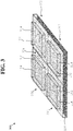
- FIG. 2A shows a top view of a semiconductor structure 100 according to various embodiments and FIG. 2B shows a bottom view of a semiconductor structure 100 according to various embodiments.
- FIG. 3 shows a semiconductor structure 300 according to various embodiments.
- the semiconductor structure 300 may include a plurality of structural elements 302, wherein each structural element of the plurality of structural elements 302 may correspond to the semiconductor structure 100.
- the semiconductor structure 300 may include a plurality of the semiconductor structures 100.
- the semiconductor structure 300 may include a plurality of antenna elements, wherein each antenna element of the plurality of antenna elements may correspond to the antenna element 112.
- the metal layer stack 108 disposed over the first side 104 of the substrate 102 may include a plurality of antenna elements and the substrate 102 may be configured as a plurality of dielectric resonators, wherein each dielectric resonator of the plurality of dielectric resonators may be disposed above an antenna element of the plurality of antenna elements.
- the plurality of dielectric resonators may form an array of dielectric resonators.
- the array of dielectric resonators may be an array of NxM structural elements 302, wherein each, N and M, may be any natural numbers (for example an array of 1x4, 8x1, 6x2, 3x3 etc. structural elements 302).
- N and M may be a multiple of two. N and M may be equal.
- the semiconductor structure 300 may include a substrate opening structure 304.
- the substrate opening structure 304 may be disposed such that each dielectric resonator of the plurality of dielectric resonators is separated from any other dielectric resonator of the plurality of dielectric resonators.
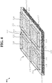
- FIG. 4 shows a semiconductor structure 400 according to various embodiments.
- the semiconductor structure 400 may correspond substantially to the semiconductor structure 300, wherein the substrate opening structure 304 may include an interconnection structure.
- the interconnection structure may include at least one substrate rail 402, 404.
- the at least one substrate rail 402, 404 may be disposed between two adjacent dielectric resonators of the plurality of dielectric resonators.
- the at least one substrate rail 402, 404 may be in contact with the two adjacent dielectric resonators.
- a substrate rail may be disposed between the centerlines of two adjacent dielectric resonators or a substrate rail may be disposed between the edge lines of two adjacent dielectric resonators.
- the interconnection structure includes a plurality of substrate rails, wherein each substrate rail of the plurality of substrate rails may be disposed between two adjacent dielectric resonators of the plurality of dielectric resonators.
- the plurality of substrate rails may include first substrate rails 402 and second substrate rails 404, wherein the first substrate rails 402 may be disposed between the centerlines of two adjacent dielectric resonators, and wherein the second substrate rails 404 may be disposed between the edge lines of two adjacent dielectric resonators.
- the interconnection structure has the effect of stabilizing the semiconductor structure.
- the plurality of dielectric resonators may form an array of dielectric resonators and the interconnection structure may include first substrate rails 402 in a first direction of the array of dielectric resonators and may include second substrate rails 404 in a second direction of the array of dielectric resonators.
- the first direction of the array of dielectric resonators may be orthogonal to the second direction of the array of dielectric resonators.
- the first direction of the array of dielectric resonators may be a horizontal in-plane direction and the second direction of the array of dielectric resonators may be a vertical in-plane direction.
- the semiconductor structure 400 may include at least one dummy dielectric resonator.
- a dummy dielectric resonator may correspond substantially to any other dielectric resonator, wherein the dummy dielectric resonator is not associated to an antenna element.
- the at least one dummy dielectric resonator may be in contact with at least one dielectric resonator of the plurality of dielectric resonators via the interconnection structure.
- the semiconductor structure 400 includes a plurality of dummy dielectric resonators. Each dummy dielectric resonator of the plurality of dummy dielectric resonators may be in contact with at least one dielectric resonator of the plurality of dielectric resonators and/or may be in contact with at least one dummy dielectric resonator via the interconnection structure.
- the plurality of dummy dielectric resonators may be substantially surrounding the array of dielectric resonators.
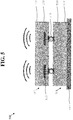
- FIG. 5 shows a system-in-package (SiP) 500 according to various embodiments.
- the SiP 500 may include an antenna chip 502.
- the antenna chip 502 may include the semiconductor structure 100, the semiconductor structure 300, and/or the semiconductor structure 400.
- the SiP 500 may further include a radio frequency integrated circuit chip 504.
- the radio frequency integrated circuit chip 504 may include a substrate 506.
- the radio frequency integrated circuit chip 504 may further include a radio frequency integrated circuit.
- the radio frequency integrated circuit chip 504 may include a radio frequency integrated circuit metal layer stack 508 disposed over the substrate 506 of the radio frequency integrated circuit chip 504.
- the radio frequency integrated circuit may be disposed at least partially within the substrate 506.
- the radio frequency integrated circuit may be disposed at least partially in the radio frequency integrated circuit metal layer stack 508.
- the active electronics of the radio frequency integrated circuit may be disposed in the substrate 506 of the radio frequency integrated circuit chip 504 and the passive electronics of the radio frequency integrated circuit may be disposed in the radio frequency integrated circuit metal layer stack 508.
- the radio frequency integrated circuit may include a radio frequency transmitter and/or a radio frequency receiver.
- the antenna chip 502 may be arranged over the radio frequency integrated circuit chip 504 such that the metal layer stack 108 of the antenna chip is facing the radio frequency integrated circuit of the radio frequency integrated circuit chip 504.
- the antenna chip 502 may be arranged over the radio frequency integrated circuit chip 504 such that the metal layer stack 108 of the antenna chip is facing the radio frequency integrated circuit metal layer stack 508.
- the size of the solder balls 510 may define the distance between the antenna chip 502 and the radio frequency integrated circuit chip 504.
- the size of the solder balls 510 may be defined such that there is no coupling between the antenna chip 502 and the radio frequency integrated circuit chip 504.
- the SiP 500 may be attached to a printed circuit board (PCB) 512.
- the SiP 500 may be attached to the PCB 512 such that the substrate 506 of the radio frequency integrated circuit chip 504 is in contact with the PCB 512.
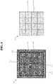
- FIG. 6 shows a top view of an antenna chip 502 and of a radio frequency integrated circuit chip 504 according to various embodiments.
- the top view of the antenna chip 502 and of a radio frequency integrated circuit chip 504 may show the surface of the respective metal layer stack.
- the radio frequency integrated circuit chip 504 may include a plurality of radio frequency contacts 602.
- the antenna chip 502 may include a plurality of feeding contacts 604.
- a radio frequency contact of the plurality of radio frequency contacts 602 of the radio frequency integrated circuit chip 504 may be aligned to an associated feeding contact of the plurality of feeding contacts 604 of the antenna chip 502.
- the plurality of radio frequency contacts 602 of the radio frequency integrated circuit chip 504 may be contacted, for example coupled, such as electrically coupled or electrically connected (for example by flip-chip contacts), to the plurality of feeding contacts 604 of the antenna chip 502.
- the plurality of solder balls 510 may be disposed between the plurality of radio frequency contacts 602 of the radio frequency integrated circuit chip 504 and the feeding contacts 604 of the antenna chip 502.
- the radio frequency integrated circuit chip 504 may have larger in-plane dimensions than the antenna chip 502.
- the radio frequency integrated circuit chip 504 may include a first region 608 and a second region 610.
- the in-plane dimensions of the first region 608 may correspond substantially to the in-plane dimensions of the antenna chip 502.
- the in-plane dimensions of the second region 610 may be larger than the in-plane dimensions of the first region 608.
- the in-plane dimensions of the second region 610 may not be in contact with the antenna chip 502.
- the radio frequency integrated circuit chip 504 may further include at least one additional contact 606.
- the at least one additional contact 606 may be one of the following: DC, clock, and/or power supply contact or contacts.
- the at least one additional contact 606 may be disposed in the second region 610 of the radio frequency integrated circuit chip 504.
- the radio frequency integrated circuit chip 504 may include a plurality of additional contacts.
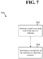
- FIG. 7 shows a method 700 for manufacturing a semiconductor structure according to various embodiments.
- the method 700 may include forming a metal layer stack 108 over a first side 104 of a substrate 102 (in 702).
- the metal layer stack 108 may include a plurality of metallization layers 110 and interdielectric layers.
- An antenna element 112 may be formed in the metal layer stack 108.
- the antenna element 112 may be configured to align the main radiation of the antenna element 112 in direction of the substrate 102.
- the method 700 may further include structuring a second side 106 of the substrate 102 as a dielectric resonator 114 (in 704).
- Structuring the second side 106 of the substrate 102 may include an etching process.
- the etching process may be a local backside etching process.
- Structuring the second side 106 of the substrate 102 may further include a wafer thinning process.
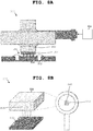
- FIG. 8A and FIG. 8B show a handling tool 800 for handling a chip according to various embodiments.
- the handling tool 800 may be a handling tool handling a chip with a backside structured substrate 802.
- the backside structured substrate 802 may include a plurality of dielectric resonators.
- the handling tool 800 may include a pumping system 804.
- the handling tool 800 may further include a suction head 806.
- the suction head 806 may include a plurality of suction points 808.
- the plurality of suction points 808 may be configured to contact the backside structured substrate 802.
- the plurality of suction points 808 may be further configured that upon contact the structures (for example the plurality of dielectric resonators) of the backside structured substrate 802 cover the suction points 808 completely.
- the size (for example diameter) of the suction points 808 is less than the size (for example diameter) of the structures (for example the dielectric resonators) of the backside structured substrate 802.
- the backside structured substrate 802 may include a plurality of structures (a plurality of structural elements), wherein the suction head 806 may be in contact with the structures (structural elements) of the backside structured substrate 802, and wherein upon contact each suction point of the plurality of suction points 808 may be covered completely by one structure (one structural element, for example one dielectric resonator) of the plurality of structures (plurality of structural elements).
- the pumping system 804 may be configured to generate a vacuum at the suction points 808.
- the handling tool 800 may be further configured to move, i.e. to handle, the chip.
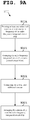
- FIG. 9A and FIG. 9B show a method 900 for mounting an antenna chip and a radio frequency integrated circuit chip on a printed circuit board according to various embodiments, wherein the method 900 is shown illustratively in FIG. 9B .
- the antenna chip may correspond substantially to the antenna chip 502, wherein at least one feeding contact 128 is disposed on top of the metal layer stack 108.
- the radio frequency integrated circuit chip may correspond substantially to the radio frequency integrated circuit chip 504, wherein the radio frequency integrated circuit chip 504 includes the first region 608 and the second region 610, wherein the in-plane dimensions of the first region 608 correspond to the in-plane dimensions of the antenna chip 502, and wherein the radio frequency integrated circuit chip 504 includes at least one radio frequency contact 602 in the first region 608 and at least one additional contact 606 disposed in the second region 610.
- the method 900 may include forming at least one solder ball 510 over the at least one radio frequency contact 602 of the radio frequency integrated circuit chip 504 (in 902A, 902B).
- the method 900 may further include arranging the radio frequency integrated circuit chip 504 over a printed circuit board (PCB) 512 (in 904A, 904B).
- the method 900 may include contacting the at least one additional contact 606 of the radio frequency integrated circuit chip 504 (in 906A, 906B).
- the at least one additional contact 606 may be contacted using wire bonding.
- the method 900 may include arranging the antenna chip 502 over the radio frequency integrated circuit chip 504 (in 908A, 908B).
- the antenna chip 502 may be arranged over the radio frequency integrated circuit chip 504 such that the at least one solder ball 510 is contacting the at least one feeding contact 604 of the antenna chip 502.
- the antenna chip 502 may be arranged over the radio frequency integrated circuit chip 504 such that the antenna chip 502 is arranged above the first region 608 of the radio frequency integrated circuit chip 504 and/or not above the second region 610 of the radio frequency integrated circuit chip 504.
- the radio frequency integrated circuit chip 504 may be arranged over the PCB 512 by arranging the radio frequency integrated circuit chip 504 in a cavity of the PCB 512.
- the antenna chip 502 may be arranged over the radio frequency integrated circuit chip 504 using a flip-chip bonding process.
- the method 900 may further include depositing material with high electrical resistivity and low coupling properties over the radio frequency integrated circuit chip 504 before arranging the antenna chip 502 over the radio frequency integrated circuit chip 504.
- FIG. 10A and FIG. 10B show a method 1000 for mounting an antenna chip and a radio frequency integrated circuit chip on a printed circuit board according to various embodiments, wherein the method 1000 is shown illustratively in FIG. 10B .
- the antenna chip may correspond substantially to the antenna chip 502, wherein at least one feeding contact 128 is disposed on top of the metal layer stack 108.
- the radio frequency integrated circuit chip may correspond substantially to the radio frequency integrated circuit chip 504, wherein the radio frequency integrated circuit chip 504 includes the first region 608 and the second region 610, wherein the in-plane dimensions of the first region 608 correspond to the in-plane dimensions of the antenna chip 502, and wherein the radio frequency integrated circuit chip 504 includes at least one radio frequency contact 602 in the first region 608 and at least one additional contact 606 disposed in the second region 610.
- the method 1000 may include arranging the radio frequency integrated circuit chip 504 over a printed circuit board (PCB) 512 (in 1002A, 1002B). The method 1000 may further include contacting the at least one additional contact 606 of the radio frequency integrated circuit chip 504 (in 1004A, 1004B). The at least one additional contact 606 may be contacted using wire bonding.
- the method 900 may include forming at least one solder ball 510 over the at least one radio frequency contact 602 of the radio frequency integrated circuit chip 504 (in 1006A, 1006B). The method 900 may include arranging the antenna chip 502 over the radio frequency integrated circuit chip 504 (in 908A, 908B.
- the antenna chip 502 may be arranged over the radio frequency integrated circuit chip 504 such that the at least one solder ball 510 is contacting the at least one feeding contact 604 of the antenna chip 502.
- the antenna chip 502 may be arranged over the radio frequency integrated circuit chip 504 such that the antenna chip 502 is arranged above the first region 608 of the radio frequency integrated circuit chip 504 and/or not above the second region 610 of the radio frequency integrated circuit chip 504.
- the radio frequency integrated circuit chip 504 may be arranged over the PCB 512 by arranging the radio frequency integrated circuit chip 504 in a cavity of the PCB 512.
- the antenna chip 502 may be arranged over the radio frequency integrated circuit chip 504 using a flip-chip bonding process.
- the method 1000 may further include depositing material with high electrical resistivity and low coupling properties over the radio frequency integrated circuit chip 504 before arranging the antenna chip 502 over the radio frequency integrated circuit chip 504.
Landscapes
- Engineering & Computer Science (AREA)
- Manufacturing & Machinery (AREA)
- Microelectronics & Electronic Packaging (AREA)
- Details Of Aerials (AREA)
- Variable-Direction Aerials And Aerial Arrays (AREA)
Abstract
Description
- Various embodiments generally relate to a semiconductor structure and a method for manufacturing a semiconductor structure.
- Radio frequency components, such as antenna elements, may be part of a semiconductor structure manufactured on a substrate. However, there may be coupling effects between the radiated waves and the substrate, such as a low-resistivity silicon substrate, leading to a reduced gain of the antenna. Thus, it may be necessary to provide a radio frequency components including semiconductor structure with reduced coupling effects.
- Previous approaches for decreasing the coupling and thus increasing the gain of an antenna are, for example, based on high resistivity substrates. However, several semiconductor processing technologies rely on low resistivity substrates.
- In various embodiments, an antenna element including semiconductor structure is provided, wherein the antenna element radiates towards the substrate, and wherein the substrate is structured as a dielectric resonator leading to reduced coupling effects and an increased gain of the antenna.
- The semiconductor structure with the features of the independent claims 1 (first example) provides an antenna structure with an increased gain.
- The substrate may include a semiconductor material, for example silicon, for example doped silicon. The substrate may include a resistivity in the range from about 0.002 Ωcm to about 75 Ωcm, for example about 30 Ωcm or higher than 30 Ωcm. The substrate may include a relative permittivity in the range from about 7 to about 16. The substrate may have a thickness in the range from about 100 µm to about 975 µm, for example 100 µm to 600 µm. The features mentioned in this paragraph in combination with the first example provide a second example.
- The metal layer stack may further include a ground plane. The feature mentioned in this paragraph in combination with the first example or the second example provides a third example.
- The antenna element may include at least one radiation slot, wherein the radiation slot may include an opening in the metal stack layer. In other words, the antenna element may be a slot-based antenna element. The at least one radiation slot may be structured in one of the following shapes:
rectangular, tapered, or curved. The dielectric resonator may resonate at the target frequency. The target frequency may be in the range from about 30 to about 500 GHz. The at least one radiation slot may have a length of about half of the wavelength (for example in the range from about one quarter to about one half of the wavelength). The length of the radiation slot may be selected depending on the dielectric layers (for example stack of dielectric layers), such as the effective permittivity of the dieletric layers. The at least one radiation slot may have a width in the range from about 10 percent to about 15 percent of the length of the at least one radiation slot. The antenna element may radiate through the at least one radiation slot. The antenna element may include at least one slot ground contact via, wherein the at least one slot ground contact via may be disposed along the edges of the at least one radiation slot. The features mentioned in this paragraph in combination with any one of the first example to the third example provide a fourth example. - The antenna element may include at least one transmission line. The transmission line may be a microstrip line, a coplanar wave guide, or a combination thereof, wherein the combination of a microstrip line and a coplanar wave guide may be a grounded coplanar wave guide. The at least one transmission line may feed the at least one radiation slot. The features mentioned in this paragraph in combination with any one of the first example to the fourth example provide a fifth example.
- The antenna element may further include at least one shorting pin. The at least one shorting pin may be disposed between the at least one transmission line and the at least one radiation slot. The features mentioned in this paragraph in combination with any one of the first example to the fifth example provide a sixth example.
- The antenna element may further include at least one feeding contact. The at least one feeding contact may feed the at least one transmission line. The at least one feeding contact may be disposed in the central part of the semiconductor structure. The at least one feeding contact may include at least one feeding contact pad. The features mentioned in this paragraph in combination with any one of the first example to the sixth example provide a seventh example.
- The antenna element may further include at least one ground contact. The at least one ground contact may include at least one ground contact pad. The antenna element may further include at least one ground contact via. The at least one ground contact via may connect the at least one ground contact to the ground plane. The features mentioned in this paragraph in combination with any one of the first example to the seventh example provide an eighth example.
- The antenna element may further include at least one antenna opening structure. The feature mentioned in this paragraph in combination with any one of the first example to the eighth example provides a ninth example.
- The dielectric resonator may enhance (in other words may shape, focus, or direct) the radiation radiated by the antenna element. The dielectric resonator may be structured in one of the following shapes: dipole, square, rectangular, triangular, circle, ring, elliptic, or n-tagonal, such as pentagonal, hexagonal, octagonal etc. The dielectric resonator may be disposed such that the radiation slot is covered by the dielectric resonator. The features mentioned in this paragraph in combination with any one of the first example to the ninth example provide a tenth example.
- The semiconductor structure may include a plurality of antenna elements. The plurality of antenna elements may realize a phased array antenna (for example the plurality of antenna elements may be part of a phased array antenna). The semiconductor structure may further include a plurality of dielectric resonators. Each dielectric resonator of the plurality of dielectric resonators may be assigned to an antenna element of the plurality of antenna elements. The plurality of dielectric resonators may form an array of dielectric resonators. The features mentioned in this paragraph in combination with any one of the first example to the tenth example provide an eleventh example.
- The semiconductor structure may further include a substrate opening structure. The substrate opening structure may be disposed such that each dielectric resonator of the plurality of dielectric resonators is separated from any other dielectric resonator of the plurality of dielectric resonators. The features mentioned in this paragraph in combination with the eleventh example provide a twelfth example.
- The semiconductor structure may further include an interconnection structure. The interconnection structure may include at least one substrate rail. This has the effect of stabilizing, for example structurally stabilizing, the semiconductor structure, for example as a chip structure. The at least one substrate rail may be disposed between two adjacent dielectric resonators. The at least one substrate rail may be in contact with the two adjacent dielectric resonators. The at least one substrate rail may be disposed between the centerlines of two adjacent dielectric resonators and/or may be disposed between the edge lines of two adjacent dielectric resonators. The features mentioned in this paragraph in combination with the twelfth example provide a thirteenth example.
- The interconnection structure may include a plurality of substrate rails. Each substrate rail of the plurality of substrate rails may be disposed between two adjacent dielectric resonators of the plurality of dielectric resonators and each substrate rail of the plurality of substrate rails may be in contact with the two adjacent dielectric resonators. Each substrate rail of the plurality of substrate rails may be disposed between the centerlines of two adjacent dielectric resonators of the plurality of dielectric resonators and/or may be disposed between the edge lines of two adjacent dielectric resonators of the plurality of dielectric resonators. The features mentioned in this paragraph in combination with the thirteenth example provide a fourteenth example.
- The plurality of substrate rails may include first substrate rails and second substrate rails, wherein first substrate rails may be disposed between the centerlines of two adjacent dielectric resonators and wherein second substrate rails may be disposed between the edge lines of two adjacent dielectric resonators. The features mentioned in this paragraph in combination with the fourteenth example provide a fifteenth example.
- The plurality of dielectric resonators may form an array of dielectric resonators and the plurality of dielectric resonators may include first substrate rails in a first direction of the array of dielectric resonators and second substrate rails in a second direction of the array of dielectric resonators. The first direction of the array of dielectric resonators may be the horizontal in-plane direction and the second direction of the array of dielectric resonators may be the vertical in-plane direction. The features mentioned in this paragraph in combination with the fifteenth example provide a sixteenth example.
- The semiconductor structure may further include at least one dummy dielectric resonator. The at least one dummy dielectric resonator may be in contact with at least one dielectric resonator via the interconnection structure. The features mentioned in this paragraph in combination with any one of the thirteenth example to the sixteenth example provide a seventeenth example.
- The semiconductor structure may include a plurality of dummy dielectric resonators. Each dummy dielectric resonator of the plurality of dummy dielectric resonators may be in contact with at least one dielectric resonator and/or at least one dummy dielectric resonator via the interconnection structure. The plurality of dummy dielectric resonators may be substantially surrounding the array of dielectric resonators. The features mentioned in this paragraph in combination with the seventeenth example provide an eighteenth example.
- An antenna chip may include the semiconductor structure of any one of the first example to the eighteenth example. The antenna chip mentioned in this paragraph provides a nineteenth example.
- A system-in-package may include an antenna chip and a radio frequency integrated circuit chip. The antenna chip may include a substrate. The substrate may include a first side and a second side. The antenna chip may further include a metal layer stack disposed over the first side of the substrate. The metal layer stack may include a plurality of metallization layers and interdielectric layers and an antenna element may be formed in the metal layer stack. The antenna element may be configured to align the main radiation direction of the antenna element in direction of the substrate. The second side of the substrate may be configured as a dielectric resonator. The radio frequency integrated circuit chip may include a substrate and may further include a radio frequency integrated circuit disposed at least partially within the substrate. The antenna chip may be arranged over the radio frequency integrated circuit chip such that the metal layer stack of the antenna chip is facing the radio frequency integrated circuit of the radio frequency integrated circuit chip. In other words, the radio frequency integrated circuit chip may include a substrate, wherein the substrate may include a first side and a second side, wherein a metal layer stack may be disposed over the first side of the substrate of the radio frequency integrated circuit chip, and wherein the antenna chip may be arranged over the radio frequency integrated circuit chip such that the metal layer stack of the antenna chip is facing the metal layer stack of the radio frequency integrated circuit chip. The system-in-package mentioned in this paragraph provides a twentieth example.
- The radio frequency integrated circuit may include a radio frequency transmitter and/or a radio frequency receiver. The radio frequency integrated circuit chip may further include a plurality of radio frequency contacts and the antenna element of the antenna chip may include a plurality of feeding contacts. The plurality of radio frequency contacts of the radio frequency integrated circuit chip may be aligned to the plurality of feeding contacts of the antenna chip. The plurality of radio frequency contacts of the radio frequency integrated circuit chip may be contacted to the plurality of feeding contacts of the antenna chip. The features mentioned in this paragraph in combination with the twentieth example provide a twenty-first example.
- The radio frequency integrated circuit chip may include larger in-plane dimensions than the antenna chip. The radio frequency integrated circuit chip may include a first region and a second region, wherein the in-plane dimensions of the first region may correspond to the in-plane dimensions of the antenna chip. The second region may be not in contact with the antenna chip. The features mentioned in this paragraph in combination with the twentieth example or the twenty-first example provide a twenty-second example.
- The radio frequency integrated circuit chip may include at least one additional contact. The at least one additional contact may be one of the following: DC, clock, and/or power supply contact/contacts. The at least one additional contact may be disposed in the second region of the radio frequency integrated circuit chip. The features mentioned in this paragraph in combination with the twenty-second example provide a twenty-third example.
- The system-in-package may be attached to a printed circuit board such that the substrate of the radio frequency integrated circuit chip is in contact with the printed circuit board. The feature mentioned in this paragraph in combination with any one of the twentieth example to the twenty-third example provide a twenty-fourth example.
- A method for manufacturing a semiconductor structure may include forming a metal layer stack over a first side of a substrate. The metal layer stack may include a plurality of metallization layers and interdielectric layers and an antenna element may be formed in the metal layer stack. The antenna element may be configured to align the main radiation direction of the antenna element in direction of the substrate. The method may further include structuring a second side of the substrate as a dielectric resonator. The method mentioned in this paragraph provides a twenty-fifth example.
- The structuring of the second side of the substrate may include an etching process. The etching process may be a local backside etching process. The method may further include a wafer thinning process. The features mentioned in this paragraph in combination with the twenty-fifth example provide a twenty-sixth example.
- A chip may include a backside structured substrate and a handling tool for handling the chip may include a pumping system. The handling tool may further include a suction head. The suction head may include a plurality of suction points, wherein the suction points may be configured to contact the backside structured substrate and that upon contact the structures of the backside structured substrate may cover the suction points completely. The pumping system may be configured to generate a vacuum at the suction points. The handling tool mentioned in this paragraph provides a twenty-seventh example.
- The backside structured substrate may include a plurality of dielectric resonators. The feature mentioned in this paragraph in combination with the twenty-seventh example provides a twenty-eighth example.
- An antenna chip may include: a substrate, including a first side and a second side; a metal layer stack disposed over the first side of the substrate, wherein the metal layer stack may include a plurality of metallization layers and interdielectric layers and wherein an antenna element may be formed in the metal layer stack; at least one feeding contact disposed on top of the metal layer stack. The antenna element may be configured to align the main radiation direction of the antenna element in direction of the substrate and the second side of the substrate may be configured as a dielectric resonator. A radio frequency integrated circuit chip may include a substrate, including a first side and a second side; a radio frequency integrated circuit disposed at least partially over the first side of the substrate; a first region and a second region, wherein the in-plane dimensions of the first region may correspond to the in-plane dimensions of the antenna chip. The radio frequency integrated circuit may include at least one radio frequency contact in the first region and at least one additional contact, wherein the at least one additional contact may be disposed in the second region. In other words, the radio frequency integrated circuit chip may include a metal layer stack disposed over the first side of the substrate of the radio frequency integrated circuit chip, wherein the at least one radio frequency contact and/or the at least one additional contact may be disposed on top of the metal layer stack of the radio frequency integrated circuit chip. A method for mounting the antenna chip and the radio frequency integrated circuit chip on a printed circuit board may include forming at least one solder ball over the at least one radio frequency contact of the radio frequency integrated circuit chip. The method may further include arranging the radio frequency integrated circuit chip over a printed circuit board. The method may include contacting the at least one additional contact. The method may include arranging the antenna chip over the radio frequency integrated circuit chip such that the at least one solder ball is contacting the at least one feeding contact of the antenna chip. The method mentioned in this paragraph provides a twenty-ninth example.
- An antenna chip may include: a substrate, including a first side and a second side; a metal layer stack disposed over the first side of the substrate, wherein the metal layer stack may include a plurality of metallization layers and interdielectric layers and wherein an antenna element may be formed in the metal layer stack; at least one feeding contact disposed on top of the metal layer stack. The antenna element may be configured to align the main radiation direction of the antenna element in direction of the substrate and the second side of the substrate may be configured as a dielectric resonator. A radio frequency integrated circuit chip may include a substrate, including a first side and a second side; a radio frequency integrated circuit disposed at least partially over the first side of the substrate; a first region and a second region, wherein the in-plane dimensions of the first region may correspond to the in-plane dimensions of the antenna chip. The radio frequency integrated circuit may include at least one radio frequency contact in the first region and at least one additional contact, wherein the at least one additional contact may be disposed in the second region. In other words, the radio frequency integrated circuit chip may include a metal layer stack disposed over the first side of the substrate of the radio frequency integrated circuit chip, wherein the at least one radio frequency contact and/or the at least one additional contact may be disposed on top of the metal layer stack of the radio frequency integrated circuit chip. A method for mounting the antenna chip and the radio frequency integrated circuit chip on a printed circuit board may include arranging the radio frequency integrated circuit chip over a printed circuit board. The method may include contacting the at least one additional contact. The method may further include forming at least one solder ball over the at least one radio frequency contact of the radio frequency integrated circuit chip. The method may include arranging the antenna chip over the radio frequency integrated circuit chip such that the at least one solder ball is contacting the at least one feeding contact of the antenna chip. The method mentioned in this paragraph provides a thirtieth example.
- The antenna chip may be arranged over the radio frequency integrated circuit chip such that the antenna chip is arranged above the first region of the radio frequency integrated circuit chip and not above the second region of the radio frequency integrated circuit chip. The features mentioned in this paragraph in combination with the twenty-ninth example or the thirtieth example provide a thirty-first example.
- The method may further include depositing material with high electrical resistivity and low coupling properties over the radio frequency integrated circuit chip before arranging the antenna chip over the radio frequency integrated circuit chip. The features mentioned in this paragraph in combination with any one of the twenty-ninth example to the thirty-first example provide a thirty-second example.
- Arranging the radio frequency integrated circuit chip over a printed circuit board may include arranging the radio frequency integrated circuit chip in a cavity of a printed circuit board. The feature mentioned in this paragraph in combination with any one of the twenty-ninth example to the thirty-second example provides a thirty-third example.
- Contacting the at least one additional contact may include wire bonding. The feature mentioned in this paragraph in combination with any one of the twenty-ninth example to the thirty-third example provides a thirty-fourth example.
- Arranging the antenna chip over the radio frequency integrated circuit chip may include a flip-chip bonding process. The feature mentioned in this paragraph in combination with any one of the twenty-ninth example to the thirty-fourth example provides a thirty-fifth example.
- Various embodiments of the invention are described with reference to the following drawings, in which:
- Figure 1
- shows a semiconductor structure according to various embodiments;
- Figure 2A
- shows a top view of a semiconductor structure according to various embodiments;
- Figure 2B
- shows a bottom view of a semiconductor structure according to various embodiments;
- Figure 3
- shows a bottom view of a semiconductor structure according to various embodiments;
- Figure 4
- shows a bottom view of a semiconductor structure according to various embodiments;
- Figure 5
- shows a system-in-package according to various embodiments;
- Figure 6
- shows a top view of an antenna chip and a radio frequency integrated circuit chip according to various embodiments;
- Figure 7
- shows a method for manufacturing a semiconductor structure according to various embodiments;
- Figure 8A
- shows a handling tool for handling a chip according to various embodiments;
- Figure 8B
- shows a handling tool according to various embodiments;
- Figure 9A
- shows a method for mounting an antenna chip according to various embodiments;
- Figure 9B
- shows a method for mounting an antenna chip according to various embodiments;
- Figure 10A
- shows a method for mounting an antenna chip according to various embodiments;
- Figure 10B
- shows a method for mounting an antenna chip according to various embodiments.
- The following detailed description refers to the accompanying drawings that show, by way of illustration, specific details and embodiments in which the invention may be practiced. These embodiments are described in sufficient detail to enable those skilled in the art to practice the invention. Other embodiments may be utilized and structural, logical, and electrical changes may be made without departing from the scope of the invention. The word "over", used herein to describe forming a feature, e.g. a layer "over" a side or surface, may be used to mean that the feature, e.g. the layer, may be formed "directly on", e.g. in direct contact with, the implied side or surface. The word "over", used herein to describe forming a feature, e.g. a layer "over" a side or surface, may be used to mean that the feature, e.g. the layer, may be formed "indirectly on" the implied side or surface with one or more additional layers being arranged between the implied side or surface and the formed layer. The term "lateral" used with regards to the "lateral" extension of a structure (or of a structure element) provided on or in a carrier (a substrate, a wafer, or another workpiece) or "laterally" next to, may be used herein to mean an extension or a positional relationship along a surface of the carrier. That means that a surface of a carrier (e.g. a surface of a substrate, a surface of a wafer, or a surface of another workpiece) may serve as reference, commonly referred to as the main processing surface. Further, the term "width" used with regards to a "width" of a structure (or of a structure element) may be used herein to mean the lateral extension of a structure. The term "thickness" used with regards to a "thickness" of a layer may be used herein to mean the spatial extension of the layer perpendicular to the surface of the support (the material or material structure) on which the layer is deposited. The term "coupled" is used herein to mean electrically connected, which may include a direct connection or an indirect connection, wherein an indirect connection may only include additional structures in the current path that not influence the substantial functioning of the described circuit or device. The terms "coupled" or "connected" may also include a physical connection. The terms "coupled" or "connected" may also include connections to transfer radio waves.
- Various embodiments relate to an antenna structure on a substrate, wherein an antenna element radiates towards the substrate and wherein the substrate is configured as a dielectric resonator.
-
FIG. 1 shows asemiconductor structure 100 according to various embodiments. Thesemiconductor structure 100 may include asubstrate 102. Thesubstrate 102 may be doped with doping atoms. Thesubstrate 102 may include a semiconductor material, such as a semiconductor material with dielectric properties, for example silicon or doped silicon. Thesubstrate 102 may include silicon. Thesubstrate 102 may include doped silicon. Thesubstrate 102 may have a resistivity in the range from about 0.0002 Ωcm to about 75 Ωcm, for example about 30 Ωcm or higher than 30 Ωcm. Thesubstrate 102 may have a relative permittivity in the range from about 7 to about 16. Thesubstrate 102 may have a thickness in the range from about 100 µm to about 975 µm, for example 100 µm to 600 µm. Thesubstrate 102 may include afirst side 104 and asecond side 106. Thesemiconductor structure 100 may include ametal layer stack 108. Themetal layer stack 108 may be disposed over thefirst side 104 of thesubstrate 102. Themetal layer stack 108 may include a plurality ofmetallization layers 110 and may include a plurality of interdielectric layers, wherein an interdielectric layer may be disposed between two metallization layers of the plurality of metallization layers 110. Themetal layer stack 108 may include anantenna element 112. In other words, anantenna element 112 may be formed in themetal layer stack 108. Theantenna element 112 may be configured to align the main radiation direction of theantenna element 112 in direction of thesubstrate 102. Thesecond side 106 of thesubstrate 102 may be configured as adielectric resonator 114. - The
metal layer stack 108 may further include aground plane 116. Theground plane 116 may be associated to any metallization layer of the plurality ofmetallization layers 110 of themetal layer stack 108. - The
antenna element 112 may include at least oneradiation slot 118. The at least oneradiation slot 118 may include an opening in themetal layer stack 108. In other words, theantenna element 112 may be a slot-based antenna element. Theradiation slot 118 may be structured in one of the following shapes: rectangular, tapered, or curved. Thedielectric resonator 114 may be configured to resonate at a target frequency. The target frequency may be in the range from about 30 GHz to about 500 GHz, for example above 60 GHz. Thedielectric resonator 114 may be configured to enhance the radiation radiated by theantenna element 112. Thedielectric resonator 114 may be structured in one of the following shapes: dipole, square, rectangular, triangular, circle, ring, elliptic, or n-tagonal, such as pentagonal, hexagonal, octagonal etc. Thedielectric resonator 114 may be disposed such that theradiation slot 118 is covered by thedielectric resonator 114. According to various embodiments, thedieletric resonator 114 is structured as a square and the planar dimensions of thedielectric resonator 114 may be about a half of the target wavelength times about a half of the target wavelength. The thickness of thedielectric resonator 114 may be selected to define the beam width and/or the bandwidth. Theradiation slot 118 may have a length of about one half of the target wavelength. Theradiation slot 118 may have a width in the range from about 10 percent to about 15 percent of the length of theradiation slot 118. Theantenna element 112 may be configured to radiate through theradiation slot 118. Regarding the impedance matching of theantenna element 112, the size (i.e. length, width) of theradiation slot 118 and the thickness of thedielectric resonator 114 may be considered. The distance between theradiation slot 118 and thedielectric resonator 114 may play no significant role. Theantenna element 112 may include at least one slot ground contact via 120. The at least one slot ground contact via 120 may be disposed along the edges of the at least oneradiation slot 118. The antenna element 12 may further include at least onetransmission line 122. The at least onetransmission line 122 may be configured to feed the at least oneradiation slot 118. The at least onetransmission line 122 may be for example a microstrip line, a coplanar wave guide, or a combination thereof, wherein the combination of a microstrip line and a coplanar wave guide may be a grounded coplanar wave guide. Theradiation slot 118 may be disposed one or more metallization layers of themetal layer stack 108 below, i.e. in direction of thesubstrate 102, the metallization layer thetransmission line 122 is disposed in. Theantenna element 112 may include at least oneshorting pin 124. The at least oneshorting pin 124 may be disposed between the at least onetransmission line 122 and the at least oneradiation slot 118. Theantenna element 112 may further include a shorting pin contact via 126. The shorting pin contact via 126 may be disposed between the at least onetransmission line 122 and the at least oneradiation slot 118. Theantenna element 112 may include at least onefeeding contact 128. The at least onefeeding contact 128 may be configured to feed the at least onetransmission line 122. The at least onefeeding contact 128 may be disposed in the central part of thesemiconductor structure 100. The at least onefeeding contact 128 may include at least one feeding contact pad. The at least onefeeding contact 128 may be disposed at the surface of themetal layer stack 108 and may be disposed in at least one metallization layer of the plurality ofmetallization layers 110 of themetal layer stack 108. In other words, the at least onefeeding contact 128 is disposed such that thefeeding contact 128 can be contacted on top of the surface of themetal layer stack 108, for example contacted such that thefeeding contact 128 can be fed by a radio wave. Theantenna element 112 may further include at least oneground contact 130. The at least oneground contact 130 may include at least one ground contact pad. Theantenna element 112 may further include at least one ground contact via 132. The at least one ground contact via 132 may be configured to connect the at least oneground contact 130 to theground plane 116. The at least one ground contact via 132 may be configured to electrically connect, i.e. electrically couple, the at least oneground contact 130 to theground plane 116. Theantenna element 112 may further include at least oneantenna opening structure 134. -
FIG. 2A shows a top view of asemiconductor structure 100 according to various embodiments andFIG. 2B shows a bottom view of asemiconductor structure 100 according to various embodiments. -
FIG. 3 shows asemiconductor structure 300 according to various embodiments. Thesemiconductor structure 300 may include a plurality ofstructural elements 302, wherein each structural element of the plurality ofstructural elements 302 may correspond to thesemiconductor structure 100. Illustratively, thesemiconductor structure 300 may include a plurality of thesemiconductor structures 100. In other words, thesemiconductor structure 300 may include a plurality of antenna elements, wherein each antenna element of the plurality of antenna elements may correspond to theantenna element 112. In even other words, themetal layer stack 108 disposed over thefirst side 104 of thesubstrate 102 may include a plurality of antenna elements and thesubstrate 102 may be configured as a plurality of dielectric resonators, wherein each dielectric resonator of the plurality of dielectric resonators may be disposed above an antenna element of the plurality of antenna elements. The plurality of dielectric resonators may form an array of dielectric resonators. The array of dielectric resonators may be an array of NxMstructural elements 302, wherein each, N and M, may be any natural numbers (for example an array of 1x4, 8x1, 6x2, 3x3 etc. structural elements 302). N and M may be a multiple of two. N and M may be equal. - The
semiconductor structure 300 may include asubstrate opening structure 304. Thesubstrate opening structure 304 may be disposed such that each dielectric resonator of the plurality of dielectric resonators is separated from any other dielectric resonator of the plurality of dielectric resonators. -
FIG. 4 shows asemiconductor structure 400 according to various embodiments. Thesemiconductor structure 400 may correspond substantially to thesemiconductor structure 300, wherein thesubstrate opening structure 304 may include an interconnection structure. The interconnection structure may include at least onesubstrate rail substrate rail substrate rail - According to various embodiments, the interconnection structure includes a plurality of substrate rails, wherein each substrate rail of the plurality of substrate rails may be disposed between two adjacent dielectric resonators of the plurality of dielectric resonators. The plurality of substrate rails may include first substrate rails 402 and second substrate rails 404, wherein the first substrate rails 402 may be disposed between the centerlines of two adjacent dielectric resonators, and wherein the second substrate rails 404 may be disposed between the edge lines of two adjacent dielectric resonators. The interconnection structure has the effect of stabilizing the semiconductor structure. The plurality of dielectric resonators may form an array of dielectric resonators and the interconnection structure may include first substrate rails 402 in a first direction of the array of dielectric resonators and may include second substrate rails 404 in a second direction of the array of dielectric resonators. The first direction of the array of dielectric resonators may be orthogonal to the second direction of the array of dielectric resonators. The first direction of the array of dielectric resonators may be a horizontal in-plane direction and the second direction of the array of dielectric resonators may be a vertical in-plane direction. The
semiconductor structure 400 may include at least one dummy dielectric resonator. A dummy dielectric resonator may correspond substantially to any other dielectric resonator, wherein the dummy dielectric resonator is not associated to an antenna element. The at least one dummy dielectric resonator may be in contact with at least one dielectric resonator of the plurality of dielectric resonators via the interconnection structure. According to various embodiments, thesemiconductor structure 400 includes a plurality of dummy dielectric resonators. Each dummy dielectric resonator of the plurality of dummy dielectric resonators may be in contact with at least one dielectric resonator of the plurality of dielectric resonators and/or may be in contact with at least one dummy dielectric resonator via the interconnection structure. The plurality of dummy dielectric resonators may be substantially surrounding the array of dielectric resonators. -
FIG. 5 shows a system-in-package (SiP) 500 according to various embodiments. TheSiP 500 may include anantenna chip 502. Theantenna chip 502 may include thesemiconductor structure 100, thesemiconductor structure 300, and/or thesemiconductor structure 400. TheSiP 500 may further include a radio frequency integratedcircuit chip 504. The radio frequency integratedcircuit chip 504 may include asubstrate 506. The radio frequency integratedcircuit chip 504 may further include a radio frequency integrated circuit. The radio frequency integratedcircuit chip 504 may include a radio frequency integrated circuitmetal layer stack 508 disposed over thesubstrate 506 of the radio frequency integratedcircuit chip 504. The radio frequency integrated circuit may be disposed at least partially within thesubstrate 506. The radio frequency integrated circuit may be disposed at least partially in the radio frequency integrated circuitmetal layer stack 508. For example, the active electronics of the radio frequency integrated circuit may be disposed in thesubstrate 506 of the radio frequency integratedcircuit chip 504 and the passive electronics of the radio frequency integrated circuit may be disposed in the radio frequency integrated circuitmetal layer stack 508. The radio frequency integrated circuit may include a radio frequency transmitter and/or a radio frequency receiver. - The
antenna chip 502 may be arranged over the radio frequency integratedcircuit chip 504 such that themetal layer stack 108 of the antenna chip is facing the radio frequency integrated circuit of the radio frequency integratedcircuit chip 504. In other words, theantenna chip 502 may be arranged over the radio frequency integratedcircuit chip 504 such that themetal layer stack 108 of the antenna chip is facing the radio frequency integrated circuitmetal layer stack 508. - Between the
antenna chip 502 and the radio frequency integrated circuit chip 504 a plurality ofsolder balls 510 may be disposed. The size of thesolder balls 510 may define the distance between theantenna chip 502 and the radio frequency integratedcircuit chip 504. The size of thesolder balls 510 may be defined such that there is no coupling between theantenna chip 502 and the radio frequency integratedcircuit chip 504. TheSiP 500 may be attached to a printed circuit board (PCB) 512. TheSiP 500 may be attached to thePCB 512 such that thesubstrate 506 of the radio frequency integratedcircuit chip 504 is in contact with thePCB 512. -
FIG. 6 shows a top view of anantenna chip 502 and of a radio frequency integratedcircuit chip 504 according to various embodiments. The top view of theantenna chip 502 and of a radio frequency integratedcircuit chip 504 may show the surface of the respective metal layer stack. The radio frequency integratedcircuit chip 504 may include a plurality ofradio frequency contacts 602. Theantenna chip 502 may include a plurality of feedingcontacts 604. Within theSiP 500, a radio frequency contact of the plurality ofradio frequency contacts 602 of the radio frequency integratedcircuit chip 504 may be aligned to an associated feeding contact of the plurality of feedingcontacts 604 of theantenna chip 502. The plurality ofradio frequency contacts 602 of the radio frequency integratedcircuit chip 504 may be contacted, for example coupled, such as electrically coupled or electrically connected (for example by flip-chip contacts), to the plurality of feedingcontacts 604 of theantenna chip 502. The plurality ofsolder balls 510 may be disposed between the plurality ofradio frequency contacts 602 of the radio frequency integratedcircuit chip 504 and the feedingcontacts 604 of theantenna chip 502. - The radio frequency integrated
circuit chip 504 may have larger in-plane dimensions than theantenna chip 502. The radio frequency integratedcircuit chip 504 may include afirst region 608 and asecond region 610. The in-plane dimensions of thefirst region 608 may correspond substantially to the in-plane dimensions of theantenna chip 502. The in-plane dimensions of thesecond region 610 may be larger than the in-plane dimensions of thefirst region 608. The in-plane dimensions of thesecond region 610 may not be in contact with theantenna chip 502. - The radio frequency integrated
circuit chip 504 may further include at least oneadditional contact 606. The at least oneadditional contact 606 may be one of the following: DC, clock, and/or power supply contact or contacts. The at least oneadditional contact 606 may be disposed in thesecond region 610 of the radio frequency integratedcircuit chip 504. According to various embodiments, the radio frequency integratedcircuit chip 504 may include a plurality of additional contacts. -
FIG. 7 shows amethod 700 for manufacturing a semiconductor structure according to various embodiments. Themethod 700 may include forming ametal layer stack 108 over afirst side 104 of a substrate 102 (in 702). Themetal layer stack 108 may include a plurality ofmetallization layers 110 and interdielectric layers. Anantenna element 112 may be formed in themetal layer stack 108. Theantenna element 112 may be configured to align the main radiation of theantenna element 112 in direction of thesubstrate 102. Themethod 700 may further include structuring asecond side 106 of thesubstrate 102 as a dielectric resonator 114 (in 704). Structuring thesecond side 106 of thesubstrate 102 may include an etching process. The etching process may be a local backside etching process. Structuring thesecond side 106 of thesubstrate 102 may further include a wafer thinning process. -
FIG. 8A and FIG. 8B show ahandling tool 800 for handling a chip according to various embodiments. Thehandling tool 800 may be a handling tool handling a chip with a backside structuredsubstrate 802. The backside structuredsubstrate 802 may include a plurality of dielectric resonators. Thehandling tool 800 may include apumping system 804. Thehandling tool 800 may further include asuction head 806. Thesuction head 806 may include a plurality of suction points 808. The plurality of suction points 808 may be configured to contact the backside structuredsubstrate 802. The plurality of suction points 808 may be further configured that upon contact the structures (for example the plurality of dielectric resonators) of the backside structuredsubstrate 802 cover the suction points 808 completely. In other words, the size (for example diameter) of the suction points 808 is less than the size (for example diameter) of the structures (for example the dielectric resonators) of the backside structuredsubstrate 802. In even other words, the backside structuredsubstrate 802 may include a plurality of structures (a plurality of structural elements), wherein thesuction head 806 may be in contact with the structures (structural elements) of the backside structuredsubstrate 802, and wherein upon contact each suction point of the plurality of suction points 808 may be covered completely by one structure (one structural element, for example one dielectric resonator) of the plurality of structures (plurality of structural elements). Thepumping system 804 may be configured to generate a vacuum at the suction points 808. This has the effect that the contact between the suction points 808 and the chip, i.e. the backside structuredsubstrate 802, is ensured upon movement of thehandling tool 800. In other words, thehandling tool 800 may be further configured to move, i.e. to handle, the chip. -
FIG. 9A andFIG. 9B show amethod 900 for mounting an antenna chip and a radio frequency integrated circuit chip on a printed circuit board according to various embodiments, wherein themethod 900 is shown illustratively inFIG. 9B . The antenna chip may correspond substantially to theantenna chip 502, wherein at least onefeeding contact 128 is disposed on top of themetal layer stack 108. The radio frequency integrated circuit chip may correspond substantially to the radio frequency integratedcircuit chip 504, wherein the radio frequency integratedcircuit chip 504 includes thefirst region 608 and thesecond region 610, wherein the in-plane dimensions of thefirst region 608 correspond to the in-plane dimensions of theantenna chip 502, and wherein the radio frequency integratedcircuit chip 504 includes at least oneradio frequency contact 602 in thefirst region 608 and at least oneadditional contact 606 disposed in thesecond region 610. - The
method 900 may include forming at least onesolder ball 510 over the at least oneradio frequency contact 602 of the radio frequency integrated circuit chip 504 (in 902A, 902B). Themethod 900 may further include arranging the radio frequency integratedcircuit chip 504 over a printed circuit board (PCB) 512 (in 904A, 904B). Themethod 900 may include contacting the at least oneadditional contact 606 of the radio frequency integrated circuit chip 504 (in 906A, 906B). The at least oneadditional contact 606 may be contacted using wire bonding. Themethod 900 may include arranging theantenna chip 502 over the radio frequency integrated circuit chip 504 (in 908A, 908B). Theantenna chip 502 may be arranged over the radio frequency integratedcircuit chip 504 such that the at least onesolder ball 510 is contacting the at least onefeeding contact 604 of theantenna chip 502. Theantenna chip 502 may be arranged over the radio frequency integratedcircuit chip 504 such that theantenna chip 502 is arranged above thefirst region 608 of the radio frequency integratedcircuit chip 504 and/or not above thesecond region 610 of the radio frequency integratedcircuit chip 504. The radio frequency integratedcircuit chip 504 may be arranged over thePCB 512 by arranging the radio frequency integratedcircuit chip 504 in a cavity of thePCB 512. Theantenna chip 502 may be arranged over the radio frequency integratedcircuit chip 504 using a flip-chip bonding process. According to various embodiments, themethod 900 may further include depositing material with high electrical resistivity and low coupling properties over the radio frequency integratedcircuit chip 504 before arranging theantenna chip 502 over the radio frequency integratedcircuit chip 504. -
FIG. 10A andFIG. 10B show amethod 1000 for mounting an antenna chip and a radio frequency integrated circuit chip on a printed circuit board according to various embodiments, wherein themethod 1000 is shown illustratively inFIG. 10B . The antenna chip may correspond substantially to theantenna chip 502, wherein at least onefeeding contact 128 is disposed on top of themetal layer stack 108. The radio frequency integrated circuit chip may correspond substantially to the radio frequency integratedcircuit chip 504, wherein the radio frequency integratedcircuit chip 504 includes thefirst region 608 and thesecond region 610, wherein the in-plane dimensions of thefirst region 608 correspond to the in-plane dimensions of theantenna chip 502, and wherein the radio frequency integratedcircuit chip 504 includes at least oneradio frequency contact 602 in thefirst region 608 and at least oneadditional contact 606 disposed in thesecond region 610. - The
method 1000 may include arranging the radio frequency integratedcircuit chip 504 over a printed circuit board (PCB) 512 (in 1002A, 1002B). Themethod 1000 may further include contacting the at least oneadditional contact 606 of the radio frequency integrated circuit chip 504 (in 1004A, 1004B). The at least oneadditional contact 606 may be contacted using wire bonding. Themethod 900 may include forming at least onesolder ball 510 over the at least oneradio frequency contact 602 of the radio frequency integrated circuit chip 504 (in 1006A, 1006B). Themethod 900 may include arranging theantenna chip 502 over the radio frequency integrated circuit chip 504 (in 908A, 908B. Theantenna chip 502 may be arranged over the radio frequency integratedcircuit chip 504 such that the at least onesolder ball 510 is contacting the at least onefeeding contact 604 of theantenna chip 502. Theantenna chip 502 may be arranged over the radio frequency integratedcircuit chip 504 such that theantenna chip 502 is arranged above thefirst region 608 of the radio frequency integratedcircuit chip 504 and/or not above thesecond region 610 of the radio frequency integratedcircuit chip 504. The radio frequency integratedcircuit chip 504 may be arranged over thePCB 512 by arranging the radio frequency integratedcircuit chip 504 in a cavity of thePCB 512. Theantenna chip 502 may be arranged over the radio frequency integratedcircuit chip 504 using a flip-chip bonding process. According to various embodiments, themethod 1000 may further include depositing material with high electrical resistivity and low coupling properties over the radio frequency integratedcircuit chip 504 before arranging theantenna chip 502 over the radio frequency integratedcircuit chip 504.
Claims (15)
- A semiconductor structure (100), comprising:• a substrate (102), comprising a first side (104) and a second side (106);• a metal layer stack (108) disposed over the first side (104) of the substrate (102), wherein the metal layer stack (108) comprises a plurality of metallization layers (110) and interdielectric layers and wherein an antenna element (112) is formed in the metal layer stack (108);• wherein the antenna element (112) is configured to align the main radiation direction of the antenna element (112) in direction of the substrate (102); and• wherein the second side (106) of the substrate (102) is configured as a dielectric resonator (114).
- The semiconductor structure (100) of claim 1, wherein the substrate (102) comprises a semiconductor material.
- The semiconductor structure (100) of any one of claims 1 or 2, wherein the dielectric resonator (114) enhances the radiation radiated by the antenna element (112).
- The semiconductor structure (100) of any one of the claims 1 to 3, wherein the dielectric resonator (114) is structured in one of the following shapes: dipole, square, rectangular, triangular, circle, ring, elliptic, or n-tagonal, such as pentagonal, hexagonal, octagonal etc.
- The semiconductor structure (100) of any one of claims 1 to 4, wherein the second side (106) of the substrate (102) comprises a plurality of dielectric resonators and wherein the plurality of dielectric resonators optionally forms an array of dielectric resonators.
- An antenna chip comprising the semiconductor structure (100) of any one of the claims 1 to 5.
- A system-in-package, comprising an antenna chip and a radio frequency integrated circuit chip, wherein the antenna chip comprises:• a substrate (102), comprising a first side (104) and a second side (106);• an metal layer stack (108) disposed over the first side (104) of the substrate (102), wherein the metal layer stack (108) comprises a plurality of metallization layers (110) and interdielectric layers and wherein an antenna element (112) is formed in the metal layer stack (108);• wherein the antenna element (112) is configured to align the main radiation direction of the antenna element (112) in direction of the substrate (102); and• wherein the second side (106) of the substrate (102) is configured as a dielectric resonator (114);wherein the radio frequency integrated circuit chip comprises a substrate, a radio frequency integrated circuit disposed at least partially within the substrate; and
wherein the antenna chip is arranged over the radio frequency integrated circuit chip such that the metal layer stack of the antenna chip is facing the radio frequency integrated circuit of the radio frequency integrated circuit chip. - A method for manufacturing a semiconductor structure, the method comprising:• Forming a metal layer stack (108) over a first side (104) of a substrate (102), wherein the metal layer stack (108) comprises a plurality of metallization layers (110) and interdielectric layers and wherein an antenna element (112) is formed in the metal layer stack (108), wherein the antenna element (112) is configured to align the main radiation direction of the antenna element (112) in direction of the substrate (102);• Structuring a second side (106) of the substrate (102) as a dielectric resonator (114).
- The method of claim 8, wherein the structuring of the second side (106) of the substrate (102) comprises an etching process.
- The method of claim 9, wherein the etching process is a local backside etching process.
- The method of any one of claim 8 to 10, further comprising a wafer thinning process.
- A handling tool for handling a chip, wherein the chip comprises a backside structured substrate and wherein the handling tool comprises:• a pumping system;• a suction head comprising a plurality of suction points, wherein the suction points are configured to contact the backside structured substrate and that upon contact the structures of the backside structured substrate cover the suction points completely;• wherein the pumping system is configured to generate a vacuum at the suction points.
- The handling tool of claim 12, wherein the backside structured substrate comprises a plurality of dielectric resonators.
- A method for mounting an antenna chip and a radio frequency integrated circuit chip on a printed circuit board, wherein the antenna chip comprises:• a substrate, comprising a first side and a second side;• a metal layer stack disposed over the first side of the substrate, wherein the metal layer stack comprises a plurality of metallization layers and interdielectric layers and wherein an antenna element is formed in the metal layer stack;• at least one feeding contact disposed on top of the metal layer stack;• wherein the antenna element is configured to align the main radiation direction of the antenna element in direction of the substrate; and• wherein the second side of the substrate is configured as a dielectric resonator;wherein the radio frequency integrated circuit chip comprises:• a substrate, comprising a first side and a second side;• a radio frequency integrated circuit disposed at least partially over the first side of the substrate;• a first region and a second region of the radio frequency integrated circuit, wherein the in-plane dimensions of the first region correspond to the in-plane dimensions of the antenna chip;• wherein the radio frequency integrated circuit comprises at least one radio frequency contact in the first region and at least one additional contact, wherein the at least one additional contact is disposed in the second region;and wherein the method comprises:• Forming at least one solder ball over the at least one radio frequency contact of the radio frequency integrated circuit chip;• Arranging the radio frequency integrated circuit chip over a printed circuit board;• Contacting the at least one additional contact;• Arranging the antenna chip over the radio frequency integrated circuit chip such that the at least one solder ball is contacting the at least one feeding contact of the antenna chip.
- A method for mounting an antenna chip and a radio frequency integrated circuit chip on a printed circuit board, wherein the antenna chip comprises:• a substrate, comprising a first side and a second side;• a metal layer stack disposed over the first side of the substrate, wherein the metal layer stack comprises a plurality of metallization layers and interdielectric layers and wherein an antenna element is formed in the metal layer stack;• at least one feeding contact disposed on top of the metal layer stack;• wherein the antenna element is configured to align the main radiation direction of the antenna element in direction of the substrate; and• wherein the second side of the substrate is configured as a dielectric resonator;wherein the radio frequency integrated circuit chip comprises:• a substrate, comprising a first side and a second side;• a radio frequency integrated circuit disposed at least partially over the first side of the substrate;• a first region and a second region of the radio frequency integrated circuit, wherein the in-plane dimensions of the first region correspond to the in-plane dimensions of the antenna chip;• wherein the radio frequency integrated circuit comprises at least one radio frequency contact in the first region and at least one additional contact, wherein the at least one additional contact is disposed in the second region;and wherein the method comprises:• Arranging the radio frequency integrated circuit chip over a printed circuit board;• Contacting the at least one additional contact;• Forming at least one solder ball over the at least one radio frequency contact of the radio frequency integrated circuit chip;• Arranging the antenna chip over the radio frequency integrated circuit chip such that the at least one solder ball is contacting the at least one feeding contact of the antenna chip.
Priority Applications (2)
| Application Number | Priority Date | Filing Date | Title |
|---|---|---|---|
| EP19215556.2A EP3836207B1 (en) | 2019-12-12 | 2019-12-12 | Semiconductor structure and method for manufacturing a semiconductor structure |
| PCT/EP2020/083492 WO2021115793A1 (en) | 2019-12-12 | 2020-11-26 | Semiconductor structure and method for manufacturing a semiconductor structure |
Applications Claiming Priority (1)
| Application Number | Priority Date | Filing Date | Title |
|---|---|---|---|
| EP19215556.2A EP3836207B1 (en) | 2019-12-12 | 2019-12-12 | Semiconductor structure and method for manufacturing a semiconductor structure |
Publications (2)
| Publication Number | Publication Date |
|---|---|
| EP3836207A1 true EP3836207A1 (en) | 2021-06-16 |
| EP3836207B1 EP3836207B1 (en) | 2022-07-27 |
Family
ID=68887281
Family Applications (1)
| Application Number | Title | Priority Date | Filing Date |
|---|---|---|---|
| EP19215556.2A Active EP3836207B1 (en) | 2019-12-12 | 2019-12-12 | Semiconductor structure and method for manufacturing a semiconductor structure |
Country Status (2)
| Country | Link |
|---|---|
| EP (1) | EP3836207B1 (en) |
| WO (1) | WO2021115793A1 (en) |
Cited By (1)
| Publication number | Priority date | Publication date | Assignee | Title |
|---|---|---|---|---|
| CN115473045A (en) * | 2022-11-14 | 2022-12-13 | 四川斯艾普电子科技有限公司 | Miniaturized high-directivity antenna based on thick film and implementation method thereof |
Families Citing this family (2)
| Publication number | Priority date | Publication date | Assignee | Title |
|---|---|---|---|---|
| CN116387802B (en) * | 2021-12-22 | 2026-01-13 | 日月光半导体制造股份有限公司 | Semiconductor packaging device |
| JP7568187B2 (en) * | 2022-02-18 | 2024-10-16 | 広州視源電子科技股▲分▼有限公司 | Antenna Assembly and Interactive Display |
Citations (9)
| Publication number | Priority date | Publication date | Assignee | Title |
|---|---|---|---|---|
| JPH07240621A (en) * | 1994-02-25 | 1995-09-12 | Mitsubishi Electric Corp | Antenna device and power feeding device |
| US20070164420A1 (en) * | 2006-01-19 | 2007-07-19 | Chen Zhi N | Apparatus and methods for packaging dielectric resonator antennas with integrated circuit chips |
| US20120287008A1 (en) * | 2011-05-11 | 2012-11-15 | Electronics And Telecommunications Research Institute | Antenna |
| WO2017167987A1 (en) * | 2016-04-01 | 2017-10-05 | Sony Corporation | Microwave antenna apparatus, packing and manufacturing method |
| EP3346549A1 (en) * | 2017-01-05 | 2018-07-11 | Fraunhofer-Gesellschaft zur Förderung der angewandten Forschung e.V. | Electronic module with integrated antenna and method of making same |
| CN108390153A (en) * | 2018-02-08 | 2018-08-10 | 南通大学 | The restructural medium resonator antenna in broadband |
| US20180254550A1 (en) * | 2017-03-01 | 2018-09-06 | Panasonic Corporation | Antenna device |
| US20190103680A1 (en) * | 2017-09-29 | 2019-04-04 | Taiwan Semiconductor Manufacturing Co., Ltd. | 3d ic antenna array with laminated high-k dielectric |
| US20190280368A1 (en) * | 2018-03-08 | 2019-09-12 | Sony Corporation | Microwave antenna apparatus and package |
-
2019
- 2019-12-12 EP EP19215556.2A patent/EP3836207B1/en active Active
-
2020
- 2020-11-26 WO PCT/EP2020/083492 patent/WO2021115793A1/en not_active Ceased
Patent Citations (9)
| Publication number | Priority date | Publication date | Assignee | Title |
|---|---|---|---|---|
| JPH07240621A (en) * | 1994-02-25 | 1995-09-12 | Mitsubishi Electric Corp | Antenna device and power feeding device |
| US20070164420A1 (en) * | 2006-01-19 | 2007-07-19 | Chen Zhi N | Apparatus and methods for packaging dielectric resonator antennas with integrated circuit chips |
| US20120287008A1 (en) * | 2011-05-11 | 2012-11-15 | Electronics And Telecommunications Research Institute | Antenna |
| WO2017167987A1 (en) * | 2016-04-01 | 2017-10-05 | Sony Corporation | Microwave antenna apparatus, packing and manufacturing method |
| EP3346549A1 (en) * | 2017-01-05 | 2018-07-11 | Fraunhofer-Gesellschaft zur Förderung der angewandten Forschung e.V. | Electronic module with integrated antenna and method of making same |
| US20180254550A1 (en) * | 2017-03-01 | 2018-09-06 | Panasonic Corporation | Antenna device |
| US20190103680A1 (en) * | 2017-09-29 | 2019-04-04 | Taiwan Semiconductor Manufacturing Co., Ltd. | 3d ic antenna array with laminated high-k dielectric |
| CN108390153A (en) * | 2018-02-08 | 2018-08-10 | 南通大学 | The restructural medium resonator antenna in broadband |
| US20190280368A1 (en) * | 2018-03-08 | 2019-09-12 | Sony Corporation | Microwave antenna apparatus and package |
Non-Patent Citations (1)
| Title |
|---|
| HAHNEL R ET AL: "Distributed on-chip antennas to increase system bandwidth at 180 GHz", 2016 GERMAN MICROWAVE CONFERENCE (GEMIC), INSTITUT FÜR MIKROWELLEN UND ANTENNENTECHNIK - IMA, 14 March 2016 (2016-03-14), pages 161 - 164, XP032896911, DOI: 10.1109/GEMIC.2016.7461580 * |
Cited By (2)
| Publication number | Priority date | Publication date | Assignee | Title |
|---|---|---|---|---|
| CN115473045A (en) * | 2022-11-14 | 2022-12-13 | 四川斯艾普电子科技有限公司 | Miniaturized high-directivity antenna based on thick film and implementation method thereof |
| CN115473045B (en) * | 2022-11-14 | 2023-02-03 | 四川斯艾普电子科技有限公司 | Miniaturized high-directivity antenna based on thick film and implementation method thereof |
Also Published As
| Publication number | Publication date |
|---|---|
| WO2021115793A1 (en) | 2021-06-17 |
| EP3836207B1 (en) | 2022-07-27 |
Similar Documents
| Publication | Publication Date | Title |
|---|---|---|
| US20220148951A1 (en) | Semiconductor device including an antenna | |
| EP3547442B1 (en) | Antenna structure with integrated coupling element and semiconductor package using the same | |
| CN114041243B (en) | Thin antenna device | |
| US10103450B2 (en) | Integration of area efficient antennas for phased array or wafer scale array antenna applications | |
| US11005155B2 (en) | Microwave antenna apparatus and package | |
| US9985346B2 (en) | Wireless communications package with integrated antennas and air cavity | |
| US9172131B2 (en) | Semiconductor structure having aperture antenna | |
| US8754818B2 (en) | Integrated antenna structure on separate semiconductor die | |
| JP5015962B2 (en) | Electronic device, wireless communication device, and electronic package device manufacturing method (device and method for packaging an integrated circuit chip having an antenna formed from a package lead wire) | |
| US8628018B2 (en) | RFID circuit and method | |
| US20070080864A1 (en) | Broadband proximity-coupled cavity backed patch antenna | |
| EP3836207B1 (en) | Semiconductor structure and method for manufacturing a semiconductor structure | |
| US7548205B2 (en) | Wafer scale antenna module with a backside connectivity | |
| EP3349248A1 (en) | Wireless device | |
| US20240178163A1 (en) | Slot Bow-Tie Antenna On Package | |
| JP7320869B2 (en) | Antenna-in-package and radar assembly package | |
| WO2018025084A1 (en) | Radio frequency isolator | |
| CN115295998A (en) | High-gain low-sidelobe phased array antenna unit suitable for surface-mounted architecture | |
| US20260018542A1 (en) | Method of fabricating a flip-chip enhanced quad flat no-lead electronic device with conductor backed coplanar waveguide transmission line feed in multilevel package substrate | |
| CN111128971B (en) | Integrated antenna packaging structure | |
| CN102074804B (en) | Antenna and method of manufacturing the same | |
| US12489211B2 (en) | Electronic device with patch antenna in packaging substrate | |
| CN115133266A (en) | A encapsulation antenna for SIP radio frequency module | |
| CN117673721B (en) | A broadband antenna packaging structure | |
| CN115425394B (en) | Strip line based on laminated structure and laminated array antenna unit based on heterogeneous substrate three-dimensional stacking |
Legal Events
| Date | Code | Title | Description |
|---|---|---|---|
| PUAI | Public reference made under article 153(3) epc to a published international application that has entered the european phase |
Free format text: ORIGINAL CODE: 0009012 |
|
| STAA | Information on the status of an ep patent application or granted ep patent |
Free format text: STATUS: REQUEST FOR EXAMINATION WAS MADE |
|
| 17P | Request for examination filed |
Effective date: 20201127 |
|
| AK | Designated contracting states |
Kind code of ref document: A1 Designated state(s): AL AT BE BG CH CY CZ DE DK EE ES FI FR GB GR HR HU IE IS IT LI LT LU LV MC MK MT NL NO PL PT RO RS SE SI SK SM TR |
|
| RIC1 | Information provided on ipc code assigned before grant |
Ipc: H01L 25/065 20060101ALI20220112BHEP Ipc: H01L 23/00 20060101ALI20220112BHEP Ipc: H01Q 21/06 20060101ALI20220112BHEP Ipc: H01Q 21/00 20060101ALI20220112BHEP Ipc: H01Q 19/06 20060101ALI20220112BHEP Ipc: H01Q 13/10 20060101ALI20220112BHEP Ipc: H01L 23/522 20060101ALI20220112BHEP Ipc: H01L 23/66 20060101ALI20220112BHEP Ipc: H01L 25/16 20060101ALI20220112BHEP Ipc: H01Q 1/22 20060101ALI20220112BHEP Ipc: H01Q 23/00 20060101ALI20220112BHEP Ipc: H01L 23/48 20060101AFI20220112BHEP |
|
| GRAP | Despatch of communication of intention to grant a patent |
Free format text: ORIGINAL CODE: EPIDOSNIGR1 |
|
| STAA | Information on the status of an ep patent application or granted ep patent |
Free format text: STATUS: GRANT OF PATENT IS INTENDED |
|
| INTG | Intention to grant announced |
Effective date: 20220221 |
|
| GRAS | Grant fee paid |
Free format text: ORIGINAL CODE: EPIDOSNIGR3 |
|
| GRAA | (expected) grant |
Free format text: ORIGINAL CODE: 0009210 |
|
| STAA | Information on the status of an ep patent application or granted ep patent |
Free format text: STATUS: THE PATENT HAS BEEN GRANTED |
|
| AK | Designated contracting states |
Kind code of ref document: B1 Designated state(s): AL AT BE BG CH CY CZ DE DK EE ES FI FR GB GR HR HU IE IS IT LI LT LU LV MC MK MT NL NO PL PT RO RS SE SI SK SM TR |
|
| REG | Reference to a national code |
Ref country code: CH Ref legal event code: EP |
|
| REG | Reference to a national code |
Ref country code: AT Ref legal event code: REF Ref document number: 1507644 Country of ref document: AT Kind code of ref document: T Effective date: 20220815 |
|
| REG | Reference to a national code |
Ref country code: DE Ref legal event code: R096 Ref document number: 602019017446 Country of ref document: DE |
|
| REG | Reference to a national code |
Ref country code: IE Ref legal event code: FG4D |
|
| REG | Reference to a national code |
Ref country code: LT Ref legal event code: MG9D |
|
| REG | Reference to a national code |
Ref country code: NL Ref legal event code: MP Effective date: 20220727 |
|
| PG25 | Lapsed in a contracting state [announced via postgrant information from national office to epo] |
Ref country code: SE Free format text: LAPSE BECAUSE OF FAILURE TO SUBMIT A TRANSLATION OF THE DESCRIPTION OR TO PAY THE FEE WITHIN THE PRESCRIBED TIME-LIMIT Effective date: 20220727 Ref country code: RS Free format text: LAPSE BECAUSE OF FAILURE TO SUBMIT A TRANSLATION OF THE DESCRIPTION OR TO PAY THE FEE WITHIN THE PRESCRIBED TIME-LIMIT Effective date: 20220727 Ref country code: PT Free format text: LAPSE BECAUSE OF FAILURE TO SUBMIT A TRANSLATION OF THE DESCRIPTION OR TO PAY THE FEE WITHIN THE PRESCRIBED TIME-LIMIT Effective date: 20221128 Ref country code: NO Free format text: LAPSE BECAUSE OF FAILURE TO SUBMIT A TRANSLATION OF THE DESCRIPTION OR TO PAY THE FEE WITHIN THE PRESCRIBED TIME-LIMIT Effective date: 20221027 Ref country code: NL Free format text: LAPSE BECAUSE OF FAILURE TO SUBMIT A TRANSLATION OF THE DESCRIPTION OR TO PAY THE FEE WITHIN THE PRESCRIBED TIME-LIMIT Effective date: 20220727 Ref country code: LV Free format text: LAPSE BECAUSE OF FAILURE TO SUBMIT A TRANSLATION OF THE DESCRIPTION OR TO PAY THE FEE WITHIN THE PRESCRIBED TIME-LIMIT Effective date: 20220727 Ref country code: LT Free format text: LAPSE BECAUSE OF FAILURE TO SUBMIT A TRANSLATION OF THE DESCRIPTION OR TO PAY THE FEE WITHIN THE PRESCRIBED TIME-LIMIT Effective date: 20220727 Ref country code: FI Free format text: LAPSE BECAUSE OF FAILURE TO SUBMIT A TRANSLATION OF THE DESCRIPTION OR TO PAY THE FEE WITHIN THE PRESCRIBED TIME-LIMIT Effective date: 20220727 Ref country code: ES Free format text: LAPSE BECAUSE OF FAILURE TO SUBMIT A TRANSLATION OF THE DESCRIPTION OR TO PAY THE FEE WITHIN THE PRESCRIBED TIME-LIMIT Effective date: 20220727 |
|
| REG | Reference to a national code |
Ref country code: AT Ref legal event code: MK05 Ref document number: 1507644 Country of ref document: AT Kind code of ref document: T Effective date: 20220727 |
|
| PG25 | Lapsed in a contracting state [announced via postgrant information from national office to epo] |
Ref country code: PL Free format text: LAPSE BECAUSE OF FAILURE TO SUBMIT A TRANSLATION OF THE DESCRIPTION OR TO PAY THE FEE WITHIN THE PRESCRIBED TIME-LIMIT Effective date: 20220727 Ref country code: IS Free format text: LAPSE BECAUSE OF FAILURE TO SUBMIT A TRANSLATION OF THE DESCRIPTION OR TO PAY THE FEE WITHIN THE PRESCRIBED TIME-LIMIT Effective date: 20221127 Ref country code: HR Free format text: LAPSE BECAUSE OF FAILURE TO SUBMIT A TRANSLATION OF THE DESCRIPTION OR TO PAY THE FEE WITHIN THE PRESCRIBED TIME-LIMIT Effective date: 20220727 Ref country code: GR Free format text: LAPSE BECAUSE OF FAILURE TO SUBMIT A TRANSLATION OF THE DESCRIPTION OR TO PAY THE FEE WITHIN THE PRESCRIBED TIME-LIMIT Effective date: 20221028 |
|
| PG25 | Lapsed in a contracting state [announced via postgrant information from national office to epo] |
Ref country code: SM Free format text: LAPSE BECAUSE OF FAILURE TO SUBMIT A TRANSLATION OF THE DESCRIPTION OR TO PAY THE FEE WITHIN THE PRESCRIBED TIME-LIMIT Effective date: 20220727 Ref country code: RO Free format text: LAPSE BECAUSE OF FAILURE TO SUBMIT A TRANSLATION OF THE DESCRIPTION OR TO PAY THE FEE WITHIN THE PRESCRIBED TIME-LIMIT Effective date: 20220727 Ref country code: DK Free format text: LAPSE BECAUSE OF FAILURE TO SUBMIT A TRANSLATION OF THE DESCRIPTION OR TO PAY THE FEE WITHIN THE PRESCRIBED TIME-LIMIT Effective date: 20220727 Ref country code: CZ Free format text: LAPSE BECAUSE OF FAILURE TO SUBMIT A TRANSLATION OF THE DESCRIPTION OR TO PAY THE FEE WITHIN THE PRESCRIBED TIME-LIMIT Effective date: 20220727 Ref country code: AT Free format text: LAPSE BECAUSE OF FAILURE TO SUBMIT A TRANSLATION OF THE DESCRIPTION OR TO PAY THE FEE WITHIN THE PRESCRIBED TIME-LIMIT Effective date: 20220727 |
|
| REG | Reference to a national code |
Ref country code: DE Ref legal event code: R097 Ref document number: 602019017446 Country of ref document: DE |
|
| PG25 | Lapsed in a contracting state [announced via postgrant information from national office to epo] |
Ref country code: SK Free format text: LAPSE BECAUSE OF FAILURE TO SUBMIT A TRANSLATION OF THE DESCRIPTION OR TO PAY THE FEE WITHIN THE PRESCRIBED TIME-LIMIT Effective date: 20220727 Ref country code: EE Free format text: LAPSE BECAUSE OF FAILURE TO SUBMIT A TRANSLATION OF THE DESCRIPTION OR TO PAY THE FEE WITHIN THE PRESCRIBED TIME-LIMIT Effective date: 20220727 |
|
| PLBE | No opposition filed within time limit |
Free format text: ORIGINAL CODE: 0009261 |
|
| STAA | Information on the status of an ep patent application or granted ep patent |
Free format text: STATUS: NO OPPOSITION FILED WITHIN TIME LIMIT |
|
| PG25 | Lapsed in a contracting state [announced via postgrant information from national office to epo] |
Ref country code: AL Free format text: LAPSE BECAUSE OF FAILURE TO SUBMIT A TRANSLATION OF THE DESCRIPTION OR TO PAY THE FEE WITHIN THE PRESCRIBED TIME-LIMIT Effective date: 20220727 |
|
| 26N | No opposition filed |
Effective date: 20230502 |
|
| REG | Reference to a national code |
Ref country code: CH Ref legal event code: PL |
|
| PG25 | Lapsed in a contracting state [announced via postgrant information from national office to epo] |
Ref country code: SI Free format text: LAPSE BECAUSE OF FAILURE TO SUBMIT A TRANSLATION OF THE DESCRIPTION OR TO PAY THE FEE WITHIN THE PRESCRIBED TIME-LIMIT Effective date: 20220727 Ref country code: LU Free format text: LAPSE BECAUSE OF NON-PAYMENT OF DUE FEES Effective date: 20221212 |
|
| PG25 | Lapsed in a contracting state [announced via postgrant information from national office to epo] |
Ref country code: LI Free format text: LAPSE BECAUSE OF NON-PAYMENT OF DUE FEES Effective date: 20221231 Ref country code: IE Free format text: LAPSE BECAUSE OF NON-PAYMENT OF DUE FEES Effective date: 20221212 Ref country code: CH Free format text: LAPSE BECAUSE OF NON-PAYMENT OF DUE FEES Effective date: 20221231 |
|
| PG25 | Lapsed in a contracting state [announced via postgrant information from national office to epo] |
Ref country code: CY Free format text: LAPSE BECAUSE OF FAILURE TO SUBMIT A TRANSLATION OF THE DESCRIPTION OR TO PAY THE FEE WITHIN THE PRESCRIBED TIME-LIMIT Effective date: 20220727 |
|
| PG25 | Lapsed in a contracting state [announced via postgrant information from national office to epo] |
Ref country code: MK Free format text: LAPSE BECAUSE OF FAILURE TO SUBMIT A TRANSLATION OF THE DESCRIPTION OR TO PAY THE FEE WITHIN THE PRESCRIBED TIME-LIMIT Effective date: 20220727 Ref country code: HU Free format text: LAPSE BECAUSE OF FAILURE TO SUBMIT A TRANSLATION OF THE DESCRIPTION OR TO PAY THE FEE WITHIN THE PRESCRIBED TIME-LIMIT; INVALID AB INITIO Effective date: 20191212 |
|
| PG25 | Lapsed in a contracting state [announced via postgrant information from national office to epo] |
Ref country code: MC Free format text: LAPSE BECAUSE OF FAILURE TO SUBMIT A TRANSLATION OF THE DESCRIPTION OR TO PAY THE FEE WITHIN THE PRESCRIBED TIME-LIMIT Effective date: 20220727 |
|
| PG25 | Lapsed in a contracting state [announced via postgrant information from national office to epo] |
Ref country code: MC Free format text: LAPSE BECAUSE OF FAILURE TO SUBMIT A TRANSLATION OF THE DESCRIPTION OR TO PAY THE FEE WITHIN THE PRESCRIBED TIME-LIMIT Effective date: 20220727 |
|
| PG25 | Lapsed in a contracting state [announced via postgrant information from national office to epo] |
Ref country code: BG Free format text: LAPSE BECAUSE OF FAILURE TO SUBMIT A TRANSLATION OF THE DESCRIPTION OR TO PAY THE FEE WITHIN THE PRESCRIBED TIME-LIMIT Effective date: 20220727 |
|
| GBPC | Gb: european patent ceased through non-payment of renewal fee |
Effective date: 20231212 |
|
| PG25 | Lapsed in a contracting state [announced via postgrant information from national office to epo] |
Ref country code: MT Free format text: LAPSE BECAUSE OF FAILURE TO SUBMIT A TRANSLATION OF THE DESCRIPTION OR TO PAY THE FEE WITHIN THE PRESCRIBED TIME-LIMIT Effective date: 20220727 |
|
| PG25 | Lapsed in a contracting state [announced via postgrant information from national office to epo] |
Ref country code: GB Free format text: LAPSE BECAUSE OF NON-PAYMENT OF DUE FEES Effective date: 20231212 |
|
| PG25 | Lapsed in a contracting state [announced via postgrant information from national office to epo] |
Ref country code: GB Free format text: LAPSE BECAUSE OF NON-PAYMENT OF DUE FEES Effective date: 20231212 |
|
| REG | Reference to a national code |
Ref country code: DE Ref legal event code: R079 Ref document number: 602019017446 Country of ref document: DE Free format text: PREVIOUS MAIN CLASS: H01L0023480000 Ipc: H10W0072000000 |
|
| PG25 | Lapsed in a contracting state [announced via postgrant information from national office to epo] |
Ref country code: TR Free format text: LAPSE BECAUSE OF FAILURE TO SUBMIT A TRANSLATION OF THE DESCRIPTION OR TO PAY THE FEE WITHIN THE PRESCRIBED TIME-LIMIT Effective date: 20220727 |
|
| PGFP | Annual fee paid to national office [announced via postgrant information from national office to epo] |
Ref country code: DE Payment date: 20251021 Year of fee payment: 7 |
|
| PGFP | Annual fee paid to national office [announced via postgrant information from national office to epo] |
Ref country code: FR Payment date: 20251217 Year of fee payment: 7 |
|
| PGFP | Annual fee paid to national office [announced via postgrant information from national office to epo] |
Ref country code: BE Payment date: 20251223 Year of fee payment: 7 |
|
| PGFP | Annual fee paid to national office [announced via postgrant information from national office to epo] |
Ref country code: IT Payment date: 20251231 Year of fee payment: 7 |