EP3835774B1 - Gas sensor - Google Patents
Gas sensor Download PDFInfo
- Publication number
- EP3835774B1 EP3835774B1 EP19847665.7A EP19847665A EP3835774B1 EP 3835774 B1 EP3835774 B1 EP 3835774B1 EP 19847665 A EP19847665 A EP 19847665A EP 3835774 B1 EP3835774 B1 EP 3835774B1
- Authority
- EP
- European Patent Office
- Prior art keywords
- thermistor
- time
- period
- detection element
- reference element
- Prior art date
- Legal status (The legal status is an assumption and is not a legal conclusion. Google has not performed a legal analysis and makes no representation as to the accuracy of the status listed.)
- Active
Links
- 238000001514 detection method Methods 0.000 claims description 61
- 238000010438 heat treatment Methods 0.000 claims description 32
- 239000007789 gas Substances 0.000 description 55
- 239000010408 film Substances 0.000 description 52
- 230000001681 protective effect Effects 0.000 description 26
- 239000000758 substrate Substances 0.000 description 18
- 239000000463 material Substances 0.000 description 15
- 230000035945 sensitivity Effects 0.000 description 15
- BASFCYQUMIYNBI-UHFFFAOYSA-N platinum Chemical compound [Pt] BASFCYQUMIYNBI-UHFFFAOYSA-N 0.000 description 12
- 239000000919 ceramic Substances 0.000 description 10
- 230000008859 change Effects 0.000 description 10
- KDLHZDBZIXYQEI-UHFFFAOYSA-N Palladium Chemical compound [Pd] KDLHZDBZIXYQEI-UHFFFAOYSA-N 0.000 description 6
- 238000000034 method Methods 0.000 description 6
- VYPSYNLAJGMNEJ-UHFFFAOYSA-N silicon dioxide Inorganic materials O=[Si]=O VYPSYNLAJGMNEJ-UHFFFAOYSA-N 0.000 description 6
- 239000010931 gold Substances 0.000 description 5
- 229910052814 silicon oxide Inorganic materials 0.000 description 5
- 230000002123 temporal effect Effects 0.000 description 5
- 238000005229 chemical vapour deposition Methods 0.000 description 4
- 230000000694 effects Effects 0.000 description 4
- 239000010410 layer Substances 0.000 description 4
- 238000005259 measurement Methods 0.000 description 4
- 229910052697 platinum Inorganic materials 0.000 description 4
- 239000004840 adhesive resin Substances 0.000 description 3
- 229920006223 adhesive resin Polymers 0.000 description 3
- 238000000151 deposition Methods 0.000 description 3
- 238000005530 etching Methods 0.000 description 3
- 229910052737 gold Inorganic materials 0.000 description 3
- 230000017525 heat dissipation Effects 0.000 description 3
- 230000004048 modification Effects 0.000 description 3
- 238000012986 modification Methods 0.000 description 3
- 230000008569 process Effects 0.000 description 3
- 230000009467 reduction Effects 0.000 description 3
- 238000005070 sampling Methods 0.000 description 3
- 239000000126 substance Substances 0.000 description 3
- ZOKXTWBITQBERF-UHFFFAOYSA-N Molybdenum Chemical compound [Mo] ZOKXTWBITQBERF-UHFFFAOYSA-N 0.000 description 2
- 229910052581 Si3N4 Inorganic materials 0.000 description 2
- 229910045601 alloy Inorganic materials 0.000 description 2
- 239000000956 alloy Substances 0.000 description 2
- 229910021417 amorphous silicon Inorganic materials 0.000 description 2
- 239000002131 composite material Substances 0.000 description 2
- 239000013078 crystal Substances 0.000 description 2
- 230000008021 deposition Effects 0.000 description 2
- 238000010586 diagram Methods 0.000 description 2
- 229910052732 germanium Inorganic materials 0.000 description 2
- GNPVGFCGXDBREM-UHFFFAOYSA-N germanium atom Chemical compound [Ge] GNPVGFCGXDBREM-UHFFFAOYSA-N 0.000 description 2
- PCHJSUWPFVWCPO-UHFFFAOYSA-N gold Chemical compound [Au] PCHJSUWPFVWCPO-UHFFFAOYSA-N 0.000 description 2
- 239000011810 insulating material Substances 0.000 description 2
- 239000011229 interlayer Substances 0.000 description 2
- 229910052741 iridium Inorganic materials 0.000 description 2
- GKOZUEZYRPOHIO-UHFFFAOYSA-N iridium atom Chemical compound [Ir] GKOZUEZYRPOHIO-UHFFFAOYSA-N 0.000 description 2
- 230000008018 melting Effects 0.000 description 2
- 238000002844 melting Methods 0.000 description 2
- 239000012528 membrane Substances 0.000 description 2
- 229910044991 metal oxide Inorganic materials 0.000 description 2
- 150000004706 metal oxides Chemical class 0.000 description 2
- 229910052750 molybdenum Inorganic materials 0.000 description 2
- 239000011733 molybdenum Substances 0.000 description 2
- 230000003647 oxidation Effects 0.000 description 2
- 238000007254 oxidation reaction Methods 0.000 description 2
- 229910052763 palladium Inorganic materials 0.000 description 2
- 229910021420 polycrystalline silicon Inorganic materials 0.000 description 2
- 229920005591 polysilicon Polymers 0.000 description 2
- 230000002441 reversible effect Effects 0.000 description 2
- HQVNEWCFYHHQES-UHFFFAOYSA-N silicon nitride Chemical compound N12[Si]34N5[Si]62N3[Si]51N64 HQVNEWCFYHHQES-UHFFFAOYSA-N 0.000 description 2
- 229910052715 tantalum Inorganic materials 0.000 description 2
- GUVRBAGPIYLISA-UHFFFAOYSA-N tantalum atom Chemical compound [Ta] GUVRBAGPIYLISA-UHFFFAOYSA-N 0.000 description 2
- 230000008646 thermal stress Effects 0.000 description 2
- 239000010409 thin film Substances 0.000 description 2
- 239000010936 titanium Substances 0.000 description 2
- WFKWXMTUELFFGS-UHFFFAOYSA-N tungsten Chemical compound [W] WFKWXMTUELFFGS-UHFFFAOYSA-N 0.000 description 2
- 229910052721 tungsten Inorganic materials 0.000 description 2
- 239000010937 tungsten Substances 0.000 description 2
- 240000006829 Ficus sundaica Species 0.000 description 1
- XUIMIQQOPSSXEZ-UHFFFAOYSA-N Silicon Chemical compound [Si] XUIMIQQOPSSXEZ-UHFFFAOYSA-N 0.000 description 1
- RTAQQCXQSZGOHL-UHFFFAOYSA-N Titanium Chemical compound [Ti] RTAQQCXQSZGOHL-UHFFFAOYSA-N 0.000 description 1
- QVGXLLKOCUKJST-UHFFFAOYSA-N atomic oxygen Chemical compound [O] QVGXLLKOCUKJST-UHFFFAOYSA-N 0.000 description 1
- 239000004020 conductor Substances 0.000 description 1
- 230000007797 corrosion Effects 0.000 description 1
- 238000005260 corrosion Methods 0.000 description 1
- 230000007423 decrease Effects 0.000 description 1
- 238000001312 dry etching Methods 0.000 description 1
- 239000011521 glass Substances 0.000 description 1
- 230000020169 heat generation Effects 0.000 description 1
- 230000006872 improvement Effects 0.000 description 1
- 238000009413 insulation Methods 0.000 description 1
- 229910052751 metal Inorganic materials 0.000 description 1
- 239000002184 metal Substances 0.000 description 1
- 239000007769 metal material Substances 0.000 description 1
- 239000001301 oxygen Substances 0.000 description 1
- 229910052760 oxygen Inorganic materials 0.000 description 1
- 239000010453 quartz Substances 0.000 description 1
- 229910052594 sapphire Inorganic materials 0.000 description 1
- 239000010980 sapphire Substances 0.000 description 1
- 229910052710 silicon Inorganic materials 0.000 description 1
- 239000010703 silicon Substances 0.000 description 1
- 238000004544 sputter deposition Methods 0.000 description 1
- 238000000992 sputter etching Methods 0.000 description 1
- 229910052719 titanium Inorganic materials 0.000 description 1
Images


Classifications
-
- G—PHYSICS
- G01—MEASURING; TESTING
- G01N—INVESTIGATING OR ANALYSING MATERIALS BY DETERMINING THEIR CHEMICAL OR PHYSICAL PROPERTIES
- G01N27/00—Investigating or analysing materials by the use of electric, electrochemical, or magnetic means
- G01N27/02—Investigating or analysing materials by the use of electric, electrochemical, or magnetic means by investigating impedance
- G01N27/04—Investigating or analysing materials by the use of electric, electrochemical, or magnetic means by investigating impedance by investigating resistance
- G01N27/14—Investigating or analysing materials by the use of electric, electrochemical, or magnetic means by investigating impedance by investigating resistance of an electrically-heated body in dependence upon change of temperature
- G01N27/18—Investigating or analysing materials by the use of electric, electrochemical, or magnetic means by investigating impedance by investigating resistance of an electrically-heated body in dependence upon change of temperature caused by changes in the thermal conductivity of a surrounding material to be tested
-
- G—PHYSICS
- G01—MEASURING; TESTING
- G01N—INVESTIGATING OR ANALYSING MATERIALS BY DETERMINING THEIR CHEMICAL OR PHYSICAL PROPERTIES
- G01N33/00—Investigating or analysing materials by specific methods not covered by groups G01N1/00 - G01N31/00
- G01N33/0004—Gaseous mixtures, e.g. polluted air
- G01N33/0009—General constructional details of gas analysers, e.g. portable test equipment
- G01N33/0027—General constructional details of gas analysers, e.g. portable test equipment concerning the detector
- G01N33/0036—General constructional details of gas analysers, e.g. portable test equipment concerning the detector specially adapted to detect a particular component
- G01N33/004—CO or CO2
Definitions
- the present invention relates to a gas sensor for detecting gas contained in the atmosphere and, more particularly, to a gas sensor configured to connect a detection element and a reference element in series.
- Gas sensors detect the concentration of a measurement target gas contained in the atmosphere.
- such gas sensor may be configured to connect a detection element and a reference element in series and acquire an output signal from the connection point therebetween.
- a gas sensor described in Patent Document 1 is configured to connect the detection element and reference element in series and heat them to their respective predetermined temperatures at detection timing.
- the gas sensor described in Patent Document 1 heats the reference element to a high temperature at non-detection timing to reduce the difference in thermal history between the detection element and the reference element.
- the gas sensor described in Patent Document 1 selectively heats only the reference element at non-detection timing, generating a difference in the number of times of heating between the detection element and the reference element. This makes it difficult to set the heating temperature and heating time of the reference element at non-detection timing and, thus, it is not easy to sufficiently reduce the difference in thermal history between the detection element and the reference element.
- a gas sensor according to the present invention is defined in claim 1.
- the reference element has a higher temperature load than the detection element in the first period of time, and the detection element has a higher temperature load than the reference element in the second period of time, so that repeating the first and second periods of time can easily reduce the difference in thermal history between the detection element and the reference element.
- control circuit may calculate the concentration of the gas to be detected based on a potential appearing at a connection point between the detection element and the reference element in one of the first and second periods of time. Thus, it is possible to calculate the concentration of the gas to be detected in one of the first and second periods of time.
- control circuit is configured to heat the first and second heaters such that the detection element and the reference element have a first temperature and a second temperature, respectively, in the first period of time and that the reference element and the detection element have the first temperature and the second temperature, respectively, in the second period of time. This allows the thermal histories of the detection element and reference element to substantially coincide with each other.
- the lengths of the first and second periods of time may be equal to each other. This allows the thermal histories of the detection element and reference element to coincide with each other more accurately.
- the gas to be detected is CO 2 gas
- the heating temperature of the detection element in the first period of time is in the range of 100°C to 200°
- the heating temperature of the reference element in the first period of time is in the range of 250°C to 350°C. This allows the concentration of CO 2 gas to be detected with high sensitivity.
- the detection element and reference element may each have a MEMS structure, and the length of the first period of time may be in the range of 50 ms to 400 ms. This can minimize power consumption.
- the ratio of the resistance value of the detection element and the resistance value of the reference element in the first period of time may be in the range of 0.5 to 2.0. This allows the concentration of CO 2 gas to be detected with high sensitivity.
- the detection element and reference element may be formed on mutually different chips. This makes the heat of the heater provided on one chip less likely to be conducted to the other chip to prevent the detection element and reference element from being suffered from thermal interference from the heaters therefor, thereby suppressing a reduction in sensitivity. Further, the difference in thermal history can be further reduced.
- the thermal histories of the detection element and reference element can be easily reduced. This can suppress the temporal change of the gas sensor.
- FIG. 1 is a circuit diagram illustrating the configuration of a gas sensor 10 according to a preferred embodiment of the present invention.
- the gas sensor 10 As illustrated in FIG. 1 , the gas sensor 10 according to the present embodiment includes a sensor part S and a control circuit 20.
- the gas sensor 10 according to the present invention detects the concentration of CO 2 gas in the atmosphere.
- the sensor part S is a heat conduction type gas sensor for detecting the concentration of CO 2 gas to be detected and has a first sensor part S1 and a second sensor part S2.
- the first sensor part S1 includes a first thermistor Rd1 serving as a detection element and a first heater resistor MH1 that heats the first thermistor Rd1.
- the second sensor part S2 includes a second thermistor Rd2 serving as a reference element and a second heater resistor MH2 that heats the second thermistor Rd2.
- the first and second thermistors Rd1 and Rd2 are connected in series between a wiring supplied with a power supply potential Vcc and a wiring supplied with a ground potential GND.
- the first and second thermistors Rd1 and Rd2 are each made of a material having a negative resistance temperature coefficient, such as a composite metal oxide, amorphous silicon, polysilicon, or germanium.
- the first thermistor Rd1 is heated by the first heater resistor MH1.
- the heating temperature of the first thermistor Rd1 by the first heater resistor MH1 is, e.g., 150°C at detection timing.
- CO 2 gas is present in the measurement atmosphere in a state where the first thermistor Rd1 is heated to 150°C, heat dissipation characteristics of the first thermistor Rd1 changes according to the CO 2 gas concentration. This change appears as a change in the resistance value of the first thermistor Rd1.
- the second thermistor Rd2 is heated by the second heater resistor MH2.
- the heating temperature of the second thermistor Rd2 by the second heater resistor MH2 is, e.g., 300°C at detection timing. Even when CO 2 gas is present in the measurement atmosphere in a state where the second thermistor Rd2 is heated to 300°C, the resistance value of the second thermistor Rd2 hardly changes.
- the ratio of the resistance value of the first thermistor Rd1 and that of the second thermistor Rd2 at a room temperature (25°C) is about 10.
- the resistance values of the first and second thermistors Rd1 and Rd2 at a room temperature are 280 kS2 and 2800 kQ, respectively.
- the heating temperature (e.g., 300°C) of the second thermistor Rd2 at detection timing is higher than the heating temperature (e.g., 150°C) of the first thermistor Rd1 at detection timing, so that, at detection timing, the ratio of the resistance value of the first thermistor Rd1 and the resistance value of the second thermistor Rd2 is in the range of 0.5 to 2.0, preferably, substantially 1.
- the resistance value of the first thermistor Rd1 heated to 150°C is 10 k ⁇
- the resistance value of the second thermistor Rd2 heated to 300°C is also 10 kS2.
- the first and second thermistors Rd1 and Rd2 are connected in series as described above, and a detection signal Vout1 is output from the connection point therebetween.
- the output detection signal Vout1 is input to the control circuit 20.
- the amount of change in the detection signal Vout1 based on the CO 2 gas concentration becomes larger as the resistance values of the first and second thermistors Rd1 and Rd2 at detection timing are closer, and detection sensitivity is improved.
- the ratio of the resistance values of the first and second thermistors Rd1 and Rd2 at detection timing is preferably in the range of 0.5 to 2.0, and particularly preferably, substantially 1.
- the control circuit 20 has differential amplifiers 21 to 23, an AD converter (ADC) 24, a DA converter (DAC) 25, a signal processing part 26, and resistors R1 to R3.
- the differential amplifier 21 compares the detection signal Vout1 and a reference voltage Vref and amplifiers the detected difference.
- the gain of the differential amplifier 21 is adjusted to any value by the resistors R1 to R3.
- An amplified signal Vamp output from the differential amplifier 21 is input to the AD converter 24.
- the AD converter 24 converts the amplified signal Vamp into a digital signal and supplies the obtained value to the signal processing part 26.
- the DA converter converts a reference signal supplied from the signal processing part 26 to an analog signal to generate the reference voltage Vref and generates control voltages Vmh1 and Vmh2 to be supplied respectively to the first and second heater resistors MH1 and MH2.
- the control voltage Vmh1 is applied to the first heater resistor MH1 through a differential amplifier 22 which is a voltage follower.
- the control voltage Vmh2 is applied to the second heater resistor MH2 through a differential amplifier 23 which is a voltage follower.
- FIG. 2 is a top view for explaining the configuration of the sensor part S.
- FIG. 3 is a cross-sectional view taken along line A-A in FIG. 2 .
- the drawings are schematic, and for explanatory convenience, the relation between thickness and plane dimension, ratio between the thicknesses of devices, and the like may be different from those in the actual structure within a range in which the effect of the present embodiment can be obtained.
- the sensor part S is a heat conduction type gas sensor that detects the concentration of a gas based on a change in heat dissipation characteristics according to the CO 2 gas concentration and has, as illustrated in FIGs. 2 and 3 , two sensor parts S1 and S2 and a ceramic package 51 housing the sensor parts S1 and S2.
- the ceramic package 51 is a box-shaped case having an opened upper part, and a lid 52 is provided at the upper part.
- the lid 52 has a plurality of vent holes 53, through which CO 2 gas in the atmosphere can flow into the ceramic package 51. In FIG. 2 , the lid 52 is omitted for ease of viewing.
- the first sensor part S1 includes insulating films 32 and 33 formed respectively on the lower and upper surfaces of a substrate 31, a first heater resistor MH1 provided on the insulating film 33, a heater protective film 34 covering the first heater resistor MH1, a first thermistor Rd1 and a thermistor electrode 35 which are provided on the heater protective film 34, a thermistor protective film 36 covering the first thermistor Rd1 and thermistor electrode 35.
- the material of the substrate 31 there is no particular restriction on the material of the substrate 31 as long as it has an adequate mechanical strength and is suitable for fine processing such as etching, and, examples thereof include a silicon single crystal substrate, a sapphire single crystal substrate, a ceramic substrate, a quartz substrate, a glass substrate, and the like.
- a cavity 31a is provided at a position overlapping the first heater resistor MH1 in a plan view so as to suppress conduction of heat due to the first heater resistor MH1 to the substrate 31.
- a part where the substrate 31 is removed by the cavity 31a is called a membrane. The presence of the membrane reduces heat capacity by the thinning of the substrate 31, allowing heating to be achieved with less power consumption.
- the insulating films 32 and 33 are each made of an insulating material such as silicon oxide or silicon nitride.
- silicon oxide is used as the insulating films 32 and 33
- a film deposition method such as a thermal oxidation method or a CVD (Chemical Vapor Deposition) method may be used.
- the thickness of the insulating films 32 and 33 is used also as an etching stop layer when the cavity 31a is formed in the substrate 31, so that the thickness thereof is preferably set to a value suitable for fulfilling the function as the etching stop layer.
- the first heater resistor MH1 is made of a conductive substance whose resistivity changes depending on temperature and is preferably made of a metal material having a comparatively high melting point, such as molybdenum (Mo), platinum (Pt), gold (Au), tungsten (W), tantalum (Ta), palladium (Pd), iridium (Ir), or an alloy containing two or more of them.
- a conductive material that can be subjected to high accuracy dry etching such as ion milling is preferable, and more preferably, it contains platinum (Pt) having high corrosion resistance as a main component.
- an adhesion layer such as a titanium (Ti) layer is preferably formed as a base of Pt so as to improve adhesion with respect to the insulating film 33.
- the heater protective film 34 is formed above the first heater resistor MH1.
- the heater protective film 34 is preferably made of the same material as the insulating film 33.
- the first heater resistor MH1 generates violent thermal changes (repetition of temperature rises between room temperature to 150°C or 300°C, for example, and then a drop to room temperature again), so that strong thermal stress is applied to the insulating film 33 and heater protective film 34.
- the insulating film 33 and heater protective film 34 may suffer damage such as interlayer peeling or crack.
- the insulating film 33 and the heater protective film 34 are made of the same material, material characteristics thereof are the same, and adhesion strength therebetween is high, so that the damage such as interlayer peeling or crack is less likely to occur as compared to when the insulating film 33 and the heater protective film 34 are made of mutually different materials.
- film deposition may be performed by a thermal oxidation method or a CVD method.
- the film thickness of the heater protective film 34 is not particularly restricted as long as insulation between the first thermistor Rd1 and the thermistor electrode 35 can be ensured and may be, e.g., 0.1 ⁇ m to 3.0 ⁇ m.
- the first thermistor Rd1 is made of a material having a negative resistance-temperature coefficient, such as a composite metal oxide, amorphous silicon, polysilicon, or germanium and can be formed by using a thin-film process such as a sputtering method or a CVD method.
- the film thickness of the first thermistor Rd1 may be adjusted according to a target resistance value.
- the reason that the thermistor is used as a temperature-sensitive resistive element is that the thermistor is larger in resistance temperature coefficient than a platinum temperature detector and can thus obtain high detection sensitivity. Further, heat generation of the first heater resistor MH1 can efficiently be detected because of the thin-film structure.
- the thermistor electrode 35 is configured of a pair of electrodes arranged spaced apart from each other at a predetermined interval, and the first thermistor Rd1 is provided between the pair of thermistor electrodes 35. With this configuration, the resistance value between the pair of thermistor electrodes 35 is determined by the resistance value of the first thermistor Rd1.
- the thermistor electrode 35 may be made of a conductive substance that can endure a process such as a film deposition step and a heat treatment process for the first thermistor Rd1 and is preferably made of a material having a comparatively high melting point, such as molybdenum (Mo), platinum (Pt), gold (Au), tungsten (W), tantalum (Ta), palladium (Pd), iridium (Ir), or an alloy containing two or more of them.
- Mo molybdenum
- platinum platinum
- Au gold
- W tungsten
- Ta tantalum
- Ir iridium
- the first thermistor Rd1 and thermistor electrode 35 are covered with the thermistor protective film 36.
- the material having reducibility so as to make it turn into a high-temperature state
- the material deprives the thermistor of oxygen to cause a reduction, thus affecting thermistor characteristics.
- an insulating oxide film having no reducibility such as silicon oxide film, is preferably used as the material of the thermistor protective film 36.
- both ends of the first heater resistor MH1 are connected respectively to electrode pads 37a and 37b provided on the surface of the thermistor protective film 36. Further, both ends of the thermistor electrode 35 are connected respectively to electrode pads 37c and 37d provided on the surface of the thermistor protective film 36.
- the electrode pads 37a to 37d are connected to a package electrode 54 installed to the ceramic package 51 through a bonding wire 55.
- the package electrode 54 is connected to the control circuit 20 illustrated in FIG. 1 through an external terminal 56 provided on the back surface of the ceramic package 51.
- the first sensor part S1 has a configuration in which the first heater resistor MH1 and first thermistor Rd1 are laminated on the substrate 31, so that heat generated by the first heater resistor MH1 is efficiently conducted to the first thermistor Rd1.
- the second sensor S2 includes insulating films 42 and 43 formed respectively on the lower and upper surfaces of a substrate 41, a second heater resistor MH2 provided on the insulating film 43, a heater protective film 44 covering the second heater resistor MH2, a second thermistor Rd2 and a thermistor electrode 45 which are provided on the heater protective film 44, and a thermistor protective film 46 covering the second thermistor Rd2 and thermistor electrode 45.
- the substrate 41 is made of the same material as the substrate 31 used for the first sensor part S1 and has the same configuration as the substrate 31. That is, a cavity 41a is provided at a position overlapping the second heater resistor MH2 in a plan view so as to suppress heat due to the second heater resistor MH2 from conducting to the substrate 41.
- the insulating films 42 and 43 are made of the same material (insulating material such as silicon oxide or silicon nitride) as the insulating films 32 and 33.
- the insulating films 42 and 43 have the same thickness as the insulating films 32 and 33.
- the second heater resistor MH2, heater protective film 44, second thermistor Rd2, thermistor electrode 45, and thermistor protective film 46 have the same configurations as the first heater resistor MH1, the heater protective film 34, the first thermistor Rd1, the thermistor electrode 35, and the thermistor protective film 36, respectively, used for the first sensor part S1.
- Both ends of the second heater resistor MH2 are connected respectively to electrode pads 47a and 47b provided on the surface of the thermistor protective film 46.
- the both ends of the thermistor electrode 45 are connected respectively to electrode pads 47c and 47d provided on the surface of the thermistor protective film 46.
- the electrode pads 47a to 47d are connected to the package electrode 54 fitted in the ceramic package 51 through the bonding wire 55.
- first and second sensor parts S1 and S2 are each produced in multiple numbers in a wafer state at a time, followed by dicing into individual pieces, and then fixed to the ceramic package 51 using a die paste (not illustrated) . Thereafter, electrode pads 37a to 37d and 47a to 47d are connected to their corresponding package electrodes 54 through the bonding wires 55 using a wire bonding machine.
- a metal having low resistance such as Au, Al, or Cu is preferably used.
- adhesive resin (not illustrated) or the like is used to fix the lid 52 having the outside air vent holes 53 to the ceramic package 51.
- a substance contained in the adhesive resin is turned into gas during heating/curing of the adhesive resin (not shown), the gas is easily discharged outside the package through the vent holes 53, so that the first and second sensor parts S1 and S2 are hardly affected.
- the thus accomplished the sensor part S is connected to the control circuit 20 or a power supply through the external terminal 56.
- the configuration of the gas sensor 10 according to the present embodiment has thus been described above.
- the first thermistor Rd1 serving as a detection element and the second thermistor Rd2 serving as a reference element are formed on mutually different chips, thus making the heat of the heater resistor provided on one chip less likely to be conducted to the other chip.
- the difference in thermal history is further reduced, resulting in a further improvement in detection accuracy.
- the gas sensor 10 utilizes a fact that the thermal conductivity of CO 2 gas significantly differs from the thermal conductivity of air to take out a change in the heat dissipation characteristics of the first and second thermistors Rd1 and Rd2 according to the CO 2 gas concentration as the detection signal Vout1.
- FIG. 4 is a graph illustrating the relationship between the heating temperature of the thermistors Rd1 and Rd2 and CO 2 sensitivity.
- the heating temperature of the thermistors Rd1 and Rd2 is in the range of 100°C to 200°C, a sufficient sensitivity to the CO 2 gas concentration can be obtained, while when the heating temperature thereof is in the range of 250°C to 300°C, the sensitivity to the CO 2 gas concentration decreases. In particular, when the heating temperature reaches 300°C, the sensitivity to the CO 2 gas concentration becomes substantially 0. Actually, a slight sensitivity to the CO 2 gas concentration exists even at a heating temperature of 300°C, but is significantly lower than the sensitivity at a heating temperature of 150°C (about 1/10 or less) and can be substantially ignored.
- the gas sensor 10 heats the first thermistor Rd1 to e.g., 150°C to sufficiently increase the sensitivity to the CO 2 gas concentration and heats the second thermistor Rd2 to, e.g., 300°C to substantially zero the sensitivity to the CO 2 gas concentration. Since the first and second thermistors Rd1 and Rd2 are connected in series, the level of the detection signal Vout1 indicates the CO 2 gas concentration.
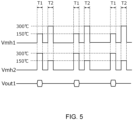
- FIG. 5 is a timing chart illustrating the waveforms of the control voltages Vmh1 and Vmh2.
- a first period of time T1 in which the control voltage Vmh1 and control voltage Vmh2 reach their respective predetermined levels at the same time and a second period of time T2 in which the control voltage Vmh1 and control voltage Vmh2 reach their respective predetermined levels at the same time are alternately repeated.
- the control voltage Vmh2 is set higher than the control voltage Vmh1, with the result that the heating temperature of the first thermistor Rd1 by the first heater resistor MH1 becomes, e.g., 150°C, and the heating temperature of the second thermistor Rd2 by the second heater resistor MH2 becomes, e.g., 300°C.
- the detection signal Vout1 is sampled by the control circuit 20, and the CO 2 gas concentration is determined based on the sampled signal.
- the sampling period of the Vout1 is, e.g., 30 sec.
- the control voltage Vmh1 is set higher than the control voltage Vmh2, with the result that the heating temperature of the first thermistor Rd1 by the first heater resistor MH1 becomes, e.g., 300°C, and the heating temperature of the second thermistor Rd2 by the second heater resistor MH2 becomes, e.g., 150°C.
- the control circuit 20 does not perform sampling of the detection signal Vout1.
- sampling of the detection signal Vout1 is not performed; however, a completely reverse temperature load to that in the first period of time T1 is applied to the first and second thermistors Rd1 and Rd2 to make the thermal histories of the first and second thermistors Rd1 and Rd2 coincide with each other. This makes it possible to easily and effectively suppress the temporal change of the gas sensor 10.
- FIG. 6 is a graph for explaining the effect of the present embodiment.
- the solid line denotes the temporal change of the gas sensor 10 according to the present embodiment
- the dashed line denotes the temporal change of the gas sensor 10 in a case where the heating operation in the second period of time T2 is omitted.
- the temporal change of the gas sensor 10 according to the present embodiment is significantly reduced as compared to when the heating operation in the second period of time T2 is omitted. This is because a completely reverse temperature load to that in the first period of time T1 is applied to the first and second thermistors Rd1 and Rd2 to make the thermal histories of the first and second thermistors Rd1 and Rd2 coincide with each other.
- the lengths of both the first and second periods of time T1 and T2 are preferably set in the range of 50 ms to 400 ms and are more preferably made to coincide with each other. That is, in the present embodiment, the first and second sensor parts S1 and S2 each have a MEMS structure, so that the time required from the start of heating by the first and second heater resistors MH1 and MH2 until the heating temperature of the first and second thermistors Rd1 and Rd2 is stabilized is about 50 ms. Further, heating beyond 400 ms, which may disadvantageously increase power consumption, is not required. Making the lengths of both the first and second periods of time T1 and T2 allows the thermal histories of the first and second thermistors Rd1 and Rd2 to completely coincide with each other.
- the timing at which the second period of time T2 is inserted is not limited unless the second period of time T2 does not overlap the first period of time T1.
- the second period of time T2 may be set immediately after the first period of time T1 so that they are continuous.
- the second period of time T2 may be inserted at a timing just corresponding to the midpoint between a given first period of time T1 and its subsequent first period of time T1.
- setting the second period of time T2 immediately before the first period of time T1 which may affect actual measurement due to residual heat in the second period of time T2, should preferably be avoided.
- first and second periods of time T1 and T2 need not be alternately repeated.
- the second period of time T2 may be inserted two times after two times of the first period of time T1.
Landscapes
- Chemical & Material Sciences (AREA)
- Health & Medical Sciences (AREA)
- Life Sciences & Earth Sciences (AREA)
- General Health & Medical Sciences (AREA)
- Immunology (AREA)
- Pathology (AREA)
- Analytical Chemistry (AREA)
- Biochemistry (AREA)
- Physics & Mathematics (AREA)
- General Physics & Mathematics (AREA)
- Chemical Kinetics & Catalysis (AREA)
- Electrochemistry (AREA)
- Engineering & Computer Science (AREA)
- Combustion & Propulsion (AREA)
- Food Science & Technology (AREA)
- Medicinal Chemistry (AREA)
- Investigating Or Analyzing Materials By The Use Of Electric Means (AREA)
Description
- The present invention relates to a gas sensor for detecting gas contained in the atmosphere and, more particularly, to a gas sensor configured to connect a detection element and a reference element in series.
- Gas sensors detect the concentration of a measurement target gas contained in the atmosphere. To improve detection accuracy, such gas sensor may be configured to connect a detection element and a reference element in series and acquire an output signal from the connection point therebetween. For example, a gas sensor described in
Patent Document 1 is configured to connect the detection element and reference element in series and heat them to their respective predetermined temperatures at detection timing. - Further, the gas sensor described in
Patent Document 1 heats the reference element to a high temperature at non-detection timing to reduce the difference in thermal history between the detection element and the reference element. - [Patent Document 1]
JP 2017-156293A - However, the gas sensor described in
Patent Document 1 selectively heats only the reference element at non-detection timing, generating a difference in the number of times of heating between the detection element and the reference element. This makes it difficult to set the heating temperature and heating time of the reference element at non-detection timing and, thus, it is not easy to sufficiently reduce the difference in thermal history between the detection element and the reference element. - It is therefore an object of the present invention to provide a gas sensor capable of reducing the difference in temperature load between the detection element and the reference element easily and more accurately.
- A gas sensor according to the present invention is defined in
claim 1. - According to the present invention, the reference element has a higher temperature load than the detection element in the first period of time, and the detection element has a higher temperature load than the reference element in the second period of time, so that repeating the first and second periods of time can easily reduce the difference in thermal history between the detection element and the reference element.
- In the present invention, the control circuit may calculate the concentration of the gas to be detected based on a potential appearing at a connection point between the detection element and the reference element in one of the first and second periods of time. Thus, it is possible to calculate the concentration of the gas to be detected in one of the first and second periods of time.
- In the present invention, the control circuit is configured to heat the first and second heaters such that the detection element and the reference element have a first temperature and a second temperature, respectively, in the first period of time and that the reference element and the detection element have the first temperature and the second temperature, respectively, in the second period of time. This allows the thermal histories of the detection element and reference element to substantially coincide with each other.
- In the present invention, the lengths of the first and second periods of time may be equal to each other. This allows the thermal histories of the detection element and reference element to coincide with each other more accurately.
- In the present invention, the gas to be detected is CO2 gas, the heating temperature of the detection element in the first period of time is in the range of 100°C to 200°, and the heating temperature of the reference element in the first period of time is in the range of 250°C to 350°C. This allows the concentration of CO2 gas to be detected with high sensitivity.
- In the present invention, the detection element and reference element may each have a MEMS structure, and the length of the first period of time may be in the range of 50 ms to 400 ms. This can minimize power consumption.
- In the present invention, the ratio of the resistance value of the detection element and the resistance value of the reference element in the first period of time may be in the range of 0.5 to 2.0. This allows the concentration of CO2 gas to be detected with high sensitivity.
- In the present invention, the detection element and reference element may be formed on mutually different chips. This makes the heat of the heater provided on one chip less likely to be conducted to the other chip to prevent the detection element and reference element from being suffered from thermal interference from the heaters therefor, thereby suppressing a reduction in sensitivity. Further, the difference in thermal history can be further reduced.
- As described above, according to the present invention, the thermal histories of the detection element and reference element can be easily reduced. This can suppress the temporal change of the gas sensor.
-
-
FIG. 1 is a circuit diagram illustrating the configuration of agas sensor 10 according to a preferred embodiment of the present invention. -
FIG. 2 is a top view for explaining the configuration of the sensor part S. -
FIG. 3 is a cross-sectional view taken along line A-A inFIG. 2 . -
FIG. 4 is a graph illustrating the relationship between the heating temperature of the thermistors Rd1 and Rd2 and CO2 sensitivity. -
FIG. 5 is a timing chart illustrating the waveforms of the control voltages Vmh1 and Vmh2. -
FIG. 6 is a graph for explaining the effect of thegas sensor 10. -
FIG. 7 is a timing chart illustrating the waveforms of the control voltages Vmh1 and Vmh2 according to a first modification. -
FIG. 8 is a timing chart illustrating the waveforms of the control voltages Vmh1 and Vmh2 according to a second modification. -
FIG. 9 is a timing chart illustrating the waveforms of the control voltages Vmh1 and Vmh2 according to a third modification. - Preferred embodiments of the present invention will be explained below in detail with reference to the accompanying drawings.
-
FIG. 1 is a circuit diagram illustrating the configuration of agas sensor 10 according to a preferred embodiment of the present invention. - As illustrated in
FIG. 1 , thegas sensor 10 according to the present embodiment includes a sensor part S and acontrol circuit 20. Thegas sensor 10 according to the present invention detects the concentration of CO2 gas in the atmosphere. - The sensor part S is a heat conduction type gas sensor for detecting the concentration of CO2 gas to be detected and has a first sensor part S1 and a second sensor part S2. The first sensor part S1 includes a first thermistor Rd1 serving as a detection element and a first heater resistor MH1 that heats the first thermistor Rd1. Similarly, the second sensor part S2 includes a second thermistor Rd2 serving as a reference element and a second heater resistor MH2 that heats the second thermistor Rd2. As illustrated in
FIG. 1 , the first and second thermistors Rd1 and Rd2 are connected in series between a wiring supplied with a power supply potential Vcc and a wiring supplied with a ground potential GND. The first and second thermistors Rd1 and Rd2 are each made of a material having a negative resistance temperature coefficient, such as a composite metal oxide, amorphous silicon, polysilicon, or germanium. - The first thermistor Rd1 is heated by the first heater resistor MH1. The heating temperature of the first thermistor Rd1 by the first heater resistor MH1 is, e.g., 150°C at detection timing. When CO2 gas is present in the measurement atmosphere in a state where the first thermistor Rd1 is heated to 150°C, heat dissipation characteristics of the first thermistor Rd1 changes according to the CO2 gas concentration. This change appears as a change in the resistance value of the first thermistor Rd1.
- The second thermistor Rd2 is heated by the second heater resistor MH2. The heating temperature of the second thermistor Rd2 by the second heater resistor MH2 is, e.g., 300°C at detection timing. Even when CO2 gas is present in the measurement atmosphere in a state where the second thermistor Rd2 is heated to 300°C, the resistance value of the second thermistor Rd2 hardly changes.
- The ratio of the resistance value of the first thermistor Rd1 and that of the second thermistor Rd2 at a room temperature (25°C) is about 10. For example, the resistance values of the first and second thermistors Rd1 and Rd2 at a room temperature are 280 kS2 and 2800 kQ, respectively. When the first and second thermistors Rd1 and Rd2 are heated, their resistance values are reduced. As described above, the heating temperature (e.g., 300°C) of the second thermistor Rd2 at detection timing is higher than the heating temperature (e.g., 150°C) of the first thermistor Rd1 at detection timing, so that, at detection timing, the ratio of the resistance value of the first thermistor Rd1 and the resistance value of the second thermistor Rd2 is in the range of 0.5 to 2.0, preferably, substantially 1. For example, the resistance value of the first thermistor Rd1 heated to 150°C is 10 kΩ, and the resistance value of the second thermistor Rd2 heated to 300°C is also 10 kS2.
- The first and second thermistors Rd1 and Rd2 are connected in series as described above, and a detection signal Vout1 is output from the connection point therebetween. The output detection signal Vout1 is input to the
control circuit 20. The amount of change in the detection signal Vout1 based on the CO2 gas concentration becomes larger as the resistance values of the first and second thermistors Rd1 and Rd2 at detection timing are closer, and detection sensitivity is improved. In this respect, the ratio of the resistance values of the first and second thermistors Rd1 and Rd2 at detection timing is preferably in the range of 0.5 to 2.0, and particularly preferably, substantially 1. - The
control circuit 20 hasdifferential amplifiers 21 to 23, an AD converter (ADC) 24, a DA converter (DAC) 25, asignal processing part 26, and resistors R1 to R3. Thedifferential amplifier 21 compares the detection signal Vout1 and a reference voltage Vref and amplifiers the detected difference. The gain of thedifferential amplifier 21 is adjusted to any value by the resistors R1 to R3. An amplified signal Vamp output from thedifferential amplifier 21 is input to theAD converter 24. - The
AD converter 24 converts the amplified signal Vamp into a digital signal and supplies the obtained value to thesignal processing part 26. On the other hand, the DA converter converts a reference signal supplied from thesignal processing part 26 to an analog signal to generate the reference voltage Vref and generates control voltages Vmh1 and Vmh2 to be supplied respectively to the first and second heater resistors MH1 and MH2. The control voltage Vmh1 is applied to the first heater resistor MH1 through adifferential amplifier 22 which is a voltage follower. Similarly, the control voltage Vmh2 is applied to the second heater resistor MH2 through adifferential amplifier 23 which is a voltage follower. -
FIG. 2 is a top view for explaining the configuration of the sensor part S.FIG. 3 is a cross-sectional view taken along line A-A inFIG. 2 . The drawings are schematic, and for explanatory convenience, the relation between thickness and plane dimension, ratio between the thicknesses of devices, and the like may be different from those in the actual structure within a range in which the effect of the present embodiment can be obtained. - The sensor part S is a heat conduction type gas sensor that detects the concentration of a gas based on a change in heat dissipation characteristics according to the CO2 gas concentration and has, as illustrated in
FIGs. 2 and3 , two sensor parts S1 and S2 and aceramic package 51 housing the sensor parts S1 and S2. - The
ceramic package 51 is a box-shaped case having an opened upper part, and alid 52 is provided at the upper part. Thelid 52 has a plurality of vent holes 53, through which CO2 gas in the atmosphere can flow into theceramic package 51. InFIG. 2 , thelid 52 is omitted for ease of viewing. - The first sensor part S1 includes insulating
films substrate 31, a first heater resistor MH1 provided on the insulatingfilm 33, a heaterprotective film 34 covering the first heater resistor MH1, a first thermistor Rd1 and athermistor electrode 35 which are provided on the heaterprotective film 34, a thermistorprotective film 36 covering the first thermistor Rd1 andthermistor electrode 35. - There is no particular restriction on the material of the
substrate 31 as long as it has an adequate mechanical strength and is suitable for fine processing such as etching, and, examples thereof include a silicon single crystal substrate, a sapphire single crystal substrate, a ceramic substrate, a quartz substrate, a glass substrate, and the like. Acavity 31a is provided at a position overlapping the first heater resistor MH1 in a plan view so as to suppress conduction of heat due to the first heater resistor MH1 to thesubstrate 31. A part where thesubstrate 31 is removed by thecavity 31a is called a membrane. The presence of the membrane reduces heat capacity by the thinning of thesubstrate 31, allowing heating to be achieved with less power consumption. - The insulating
films films films film 33 is used also as an etching stop layer when thecavity 31a is formed in thesubstrate 31, so that the thickness thereof is preferably set to a value suitable for fulfilling the function as the etching stop layer. - The first heater resistor MH1 is made of a conductive substance whose resistivity changes depending on temperature and is preferably made of a metal material having a comparatively high melting point, such as molybdenum (Mo), platinum (Pt), gold (Au), tungsten (W), tantalum (Ta), palladium (Pd), iridium (Ir), or an alloy containing two or more of them. Among them, a conductive material that can be subjected to high accuracy dry etching such as ion milling is preferable, and more preferably, it contains platinum (Pt) having high corrosion resistance as a main component. Further, an adhesion layer such as a titanium (Ti) layer is preferably formed as a base of Pt so as to improve adhesion with respect to the insulating
film 33. - The heater
protective film 34 is formed above the first heater resistor MH1. The heaterprotective film 34 is preferably made of the same material as the insulatingfilm 33. The first heater resistor MH1 generates violent thermal changes (repetition of temperature rises between room temperature to 150°C or 300°C, for example, and then a drop to room temperature again), so that strong thermal stress is applied to the insulatingfilm 33 and heaterprotective film 34. When being continuously subject to the thermal stress, the insulatingfilm 33 and heaterprotective film 34 may suffer damage such as interlayer peeling or crack. However, when the insulatingfilm 33 and the heaterprotective film 34 are made of the same material, material characteristics thereof are the same, and adhesion strength therebetween is high, so that the damage such as interlayer peeling or crack is less likely to occur as compared to when the insulatingfilm 33 and the heaterprotective film 34 are made of mutually different materials. When silicon oxide is used as the material of the heaterprotective film 34, film deposition may be performed by a thermal oxidation method or a CVD method. The film thickness of the heaterprotective film 34 is not particularly restricted as long as insulation between the first thermistor Rd1 and thethermistor electrode 35 can be ensured and may be, e.g., 0.1 µm to 3.0 µm. - The first thermistor Rd1 is made of a material having a negative resistance-temperature coefficient, such as a composite metal oxide, amorphous silicon, polysilicon, or germanium and can be formed by using a thin-film process such as a sputtering method or a CVD method. The film thickness of the first thermistor Rd1 may be adjusted according to a target resistance value. The reason that the thermistor is used as a temperature-sensitive resistive element is that the thermistor is larger in resistance temperature coefficient than a platinum temperature detector and can thus obtain high detection sensitivity. Further, heat generation of the first heater resistor MH1 can efficiently be detected because of the thin-film structure.
- The
thermistor electrode 35 is configured of a pair of electrodes arranged spaced apart from each other at a predetermined interval, and the first thermistor Rd1 is provided between the pair ofthermistor electrodes 35. With this configuration, the resistance value between the pair ofthermistor electrodes 35 is determined by the resistance value of the first thermistor Rd1. Thethermistor electrode 35 may be made of a conductive substance that can endure a process such as a film deposition step and a heat treatment process for the first thermistor Rd1 and is preferably made of a material having a comparatively high melting point, such as molybdenum (Mo), platinum (Pt), gold (Au), tungsten (W), tantalum (Ta), palladium (Pd), iridium (Ir), or an alloy containing two or more of them. - The first thermistor Rd1 and
thermistor electrode 35 are covered with the thermistorprotective film 36. When the first thermistor Rd1 is brought into contact with a material having reducibility so as to make it turn into a high-temperature state, the material deprives the thermistor of oxygen to cause a reduction, thus affecting thermistor characteristics. To prevent this, an insulating oxide film having no reducibility, such as silicon oxide film, is preferably used as the material of the thermistorprotective film 36. - As illustrated in
FIG. 2 , both ends of the first heater resistor MH1 are connected respectively toelectrode pads protective film 36. Further, both ends of thethermistor electrode 35 are connected respectively toelectrode pads protective film 36. Theelectrode pads 37a to 37d are connected to apackage electrode 54 installed to theceramic package 51 through abonding wire 55. Thepackage electrode 54 is connected to thecontrol circuit 20 illustrated inFIG. 1 through anexternal terminal 56 provided on the back surface of theceramic package 51. - As described above, the first sensor part S1 has a configuration in which the first heater resistor MH1 and first thermistor Rd1 are laminated on the
substrate 31, so that heat generated by the first heater resistor MH1 is efficiently conducted to the first thermistor Rd1. - Similarly, the second sensor S2 includes insulating
films substrate 41, a second heater resistor MH2 provided on the insulatingfilm 43, a heaterprotective film 44 covering the second heater resistor MH2, a second thermistor Rd2 and athermistor electrode 45 which are provided on the heaterprotective film 44, and a thermistorprotective film 46 covering the second thermistor Rd2 andthermistor electrode 45. - The
substrate 41 is made of the same material as thesubstrate 31 used for the first sensor part S1 and has the same configuration as thesubstrate 31. That is, acavity 41a is provided at a position overlapping the second heater resistor MH2 in a plan view so as to suppress heat due to the second heater resistor MH2 from conducting to thesubstrate 41. The insulatingfilms films films films - The second heater resistor MH2, heater
protective film 44, second thermistor Rd2,thermistor electrode 45, and thermistorprotective film 46 have the same configurations as the first heater resistor MH1, the heaterprotective film 34, the first thermistor Rd1, thethermistor electrode 35, and the thermistorprotective film 36, respectively, used for the first sensor part S1. Both ends of the second heater resistor MH2 are connected respectively toelectrode pads protective film 46. Further, the both ends of thethermistor electrode 45 are connected respectively toelectrode pads protective film 46. Theelectrode pads 47a to 47d are connected to thepackage electrode 54 fitted in theceramic package 51 through thebonding wire 55. - The thus configured first and second sensor parts S1 and S2 are each produced in multiple numbers in a wafer state at a time, followed by dicing into individual pieces, and then fixed to the
ceramic package 51 using a die paste (not illustrated) . Thereafter,electrode pads 37a to 37d and 47a to 47d are connected to theircorresponding package electrodes 54 through thebonding wires 55 using a wire bonding machine. As the material of thebonding wire 55, a metal having low resistance, such as Au, Al, or Cu is preferably used. - Finally, adhesive resin (not illustrated) or the like is used to fix the
lid 52 having the outside air vent holes 53 to theceramic package 51. Although a substance contained in the adhesive resin is turned into gas during heating/curing of the adhesive resin (not shown), the gas is easily discharged outside the package through the vent holes 53, so that the first and second sensor parts S1 and S2 are hardly affected. - The thus accomplished the sensor part S is connected to the
control circuit 20 or a power supply through theexternal terminal 56. - The configuration of the
gas sensor 10 according to the present embodiment has thus been described above. As described above, in thegas sensor 10 according to the present embodiment, the first thermistor Rd1 serving as a detection element and the second thermistor Rd2 serving as a reference element are formed on mutually different chips, thus making the heat of the heater resistor provided on one chip less likely to be conducted to the other chip. This prevents the first and second thermistors Rd1 and Rd2 from being suffered from thermal interference from the heaters therefor, thereby suppressing a reduction in sensitivity. Further, the difference in thermal history is further reduced, resulting in a further improvement in detection accuracy. - The following describes the operation of the
gas sensor 10 according to the present embodiment. - The
gas sensor 10 according to the present embodiment utilizes a fact that the thermal conductivity of CO2 gas significantly differs from the thermal conductivity of air to take out a change in the heat dissipation characteristics of the first and second thermistors Rd1 and Rd2 according to the CO2 gas concentration as the detection signal Vout1. -
FIG. 4 is a graph illustrating the relationship between the heating temperature of the thermistors Rd1 and Rd2 and CO2 sensitivity. - As illustrated in
FIG. 4 , when the heating temperature of the thermistors Rd1 and Rd2 is in the range of 100°C to 200°C, a sufficient sensitivity to the CO2 gas concentration can be obtained, while when the heating temperature thereof is in the range of 250°C to 300°C, the sensitivity to the CO2 gas concentration decreases. In particular, when the heating temperature reaches 300°C, the sensitivity to the CO2 gas concentration becomes substantially 0. Actually, a slight sensitivity to the CO2 gas concentration exists even at a heating temperature of 300°C, but is significantly lower than the sensitivity at a heating temperature of 150°C (about 1/10 or less) and can be substantially ignored. - Considering the above, at detection timing, the
gas sensor 10 according to the present embodiment heats the first thermistor Rd1 to e.g., 150°C to sufficiently increase the sensitivity to the CO2 gas concentration and heats the second thermistor Rd2 to, e.g., 300°C to substantially zero the sensitivity to the CO2 gas concentration. Since the first and second thermistors Rd1 and Rd2 are connected in series, the level of the detection signal Vout1 indicates the CO2 gas concentration. -
FIG. 5 is a timing chart illustrating the waveforms of the control voltages Vmh1 and Vmh2. - As illustrated in
FIG. 5 , in the present embodiment, a first period of time T1 in which the control voltage Vmh1 and control voltage Vmh2 reach their respective predetermined levels at the same time and a second period of time T2 in which the control voltage Vmh1 and control voltage Vmh2 reach their respective predetermined levels at the same time are alternately repeated. In the first period of time 11, the control voltage Vmh2 is set higher than the control voltage Vmh1, with the result that the heating temperature of the first thermistor Rd1 by the first heater resistor MH1 becomes, e.g., 150°C, and the heating temperature of the second thermistor Rd2 by the second heater resistor MH2 becomes, e.g., 300°C. In the first period of time T1, the detection signal Vout1 is sampled by thecontrol circuit 20, and the CO2 gas concentration is determined based on the sampled signal. The sampling period of the Vout1 is, e.g., 30 sec. - In the second period of time T2, the control voltage Vmh1 is set higher than the control voltage Vmh2, with the result that the heating temperature of the first thermistor Rd1 by the first heater resistor MH1 becomes, e.g., 300°C, and the heating temperature of the second thermistor Rd2 by the second heater resistor MH2 becomes, e.g., 150°C. In the second period of time T2, the
control circuit 20 does not perform sampling of the detection signal Vout1. - Thus, in the second period of time T2, sampling of the detection signal Vout1 is not performed; however, a completely reverse temperature load to that in the first period of time T1 is applied to the first and second thermistors Rd1 and Rd2 to make the thermal histories of the first and second thermistors Rd1 and Rd2 coincide with each other. This makes it possible to easily and effectively suppress the temporal change of the
gas sensor 10. -
FIG. 6 is a graph for explaining the effect of the present embodiment. The solid line denotes the temporal change of thegas sensor 10 according to the present embodiment, and the dashed line denotes the temporal change of thegas sensor 10 in a case where the heating operation in the second period of time T2 is omitted. As can be seen fromFIG. 6 , the temporal change of thegas sensor 10 according to the present embodiment is significantly reduced as compared to when the heating operation in the second period of time T2 is omitted. This is because a completely reverse temperature load to that in the first period of time T1 is applied to the first and second thermistors Rd1 and Rd2 to make the thermal histories of the first and second thermistors Rd1 and Rd2 coincide with each other. - The lengths of both the first and second periods of time T1 and T2 are preferably set in the range of 50 ms to 400 ms and are more preferably made to coincide with each other. That is, in the present embodiment, the first and second sensor parts S1 and S2 each have a MEMS structure, so that the time required from the start of heating by the first and second heater resistors MH1 and MH2 until the heating temperature of the first and second thermistors Rd1 and Rd2 is stabilized is about 50 ms. Further, heating beyond 400 ms, which may disadvantageously increase power consumption, is not required. Making the lengths of both the first and second periods of time T1 and T2 allows the thermal histories of the first and second thermistors Rd1 and Rd2 to completely coincide with each other.
- The timing at which the second period of time T2 is inserted is not limited unless the second period of time T2 does not overlap the first period of time T1. Thus, as illustrated in
FIG. 7 , the second period of time T2 may be set immediately after the first period of time T1 so that they are continuous. Alternatively, as illustrated inFIG. 8 , the second period of time T2 may be inserted at a timing just corresponding to the midpoint between a given first period of time T1 and its subsequent first period of time T1. However, setting the second period of time T2 immediately before the first period of time T1, which may affect actual measurement due to residual heat in the second period of time T2, should preferably be avoided. - Further, the first and second periods of time T1 and T2 need not be alternately repeated. For example, as illustrated in
FIG. 9 , the second period of time T2 may be inserted two times after two times of the first period of time T1. - It is apparent that the present invention is not limited to the above embodiments, but may be modified and changed without departing from the scope of the invention.
-
- 20
- control circuit
- 21-23
- differential amplifier
- 24
- AD converter
- 25
- DA converter
- 26
- signal processing part
- 31, 41
- substrate
- 31a, 41a
- cavity
- 32, 33, 42, 43
- insulating film
- 34, 44
- heater protective film
- 35, 45
- thermistor electrode
- 36, 46
- thermistor protective film
- 37a-37d, 47a-47
- delectrode pad
- 51
- ceramic package
- 52
- lid
- 53
- vent hole
- 54
- package electrode
- 55
- bonding wire
- 56
- external terminal
- MH1
- first heater resistor
- MH2
- second heater resistor
- R1-R3
- resistor
- Rd1
- first thermistor (detection element)
- Rd2
- second thermistor (reference element)
- S
- sensor part
- S1
- first sensor part
- S2
- second sensor part
- T1
- first period of time
- T2
- second period of time
Claims (6)
- A gas sensor comprising:a detection element (Rd1) whose resistance value changes in accordance with a concentration of CO2 gas;a reference element (Rd2) connected in series to the detection element;a first heater (MH1) for heating the detection element;a second heater (MH2) for heating the reference element; anda control circuit (20) configured to heat the first and second heaters such that the reference element has a higher temperature than the detection element in a first period of time and that the detection element has a higher temperature than the reference element in a second period of time,wherein the control circuit is configured to heat the first and second heaters such that the detection element and the reference element have a first temperature and a second temperature, respectively, in the first period of time and that the reference element and the detection element have the first temperature and the second temperature, respectively, in the second period of time;wherein the heating temperature of the detection element in the first period of time is in a range of 100°C to 200°; andwherein the heating temperature of the reference element in the first period of time is in a range of 250°C to 350°C.
- The gas sensor as claimed in claim 1, wherein the control circuit is configured to calculate the concentration of CO2 gas based on a potential appearing at a connection point between the detection element and the reference element in one of the first and second periods of time.
- The gas sensor as claimed in claim 1 or 2, wherein lengths of the first and second periods of time are equal to each other.
- The gas sensor as claimed in any one of claims 1 to 3,wherein the detection element and reference element have a MEMS structure, andwherein a length of the first period of time is in a range of 50 ms to 400 ms.
- The gas sensor as claimed in any one of claims 1 to 4, wherein a ratio of a resistance value of the detection element and a resistance value of the reference element in the first period of time is in a range of 0.5 to 2.0.
- The gas sensor as claimed in any one of claims 1 to 5, wherein the detection element and reference element are formed on mutually different chips.
Applications Claiming Priority (2)
| Application Number | Priority Date | Filing Date | Title |
|---|---|---|---|
| JP2018151364 | 2018-08-10 | ||
| PCT/JP2019/024432 WO2020031517A1 (en) | 2018-08-10 | 2019-06-20 | Gas sensor |
Publications (3)
| Publication Number | Publication Date |
|---|---|
| EP3835774A1 EP3835774A1 (en) | 2021-06-16 |
| EP3835774A4 EP3835774A4 (en) | 2022-04-20 |
| EP3835774B1 true EP3835774B1 (en) | 2024-07-31 |
Family
ID=69415520
Family Applications (1)
| Application Number | Title | Priority Date | Filing Date |
|---|---|---|---|
| EP19847665.7A Active EP3835774B1 (en) | 2018-08-10 | 2019-06-20 | Gas sensor |
Country Status (5)
| Country | Link |
|---|---|
| US (1) | US11567025B2 (en) |
| EP (1) | EP3835774B1 (en) |
| JP (1) | JP7188445B2 (en) |
| CN (1) | CN112585455A (en) |
| WO (1) | WO2020031517A1 (en) |
Families Citing this family (8)
| Publication number | Priority date | Publication date | Assignee | Title |
|---|---|---|---|---|
| JP7235057B2 (en) * | 2018-12-17 | 2023-03-08 | Tdk株式会社 | gas sensor |
| JP7287344B2 (en) * | 2020-05-13 | 2023-06-06 | Tdk株式会社 | gas sensor |
| DE102022107394A1 (en) * | 2021-03-30 | 2022-10-06 | Tdk Electronics Ag | Sensor system, sensor arrangement and method of using the sensor system |
| CN113671000A (en) * | 2021-07-27 | 2021-11-19 | 浙江华才检测技术有限公司 | Matrix type broad-spectrum substance detection sensor built based on semiconductor functional material |
| WO2024105868A1 (en) * | 2022-11-18 | 2024-05-23 | Tdk株式会社 | Gas sensor |
| WO2024111024A1 (en) * | 2022-11-21 | 2024-05-30 | Tdk株式会社 | Gas sensor |
| WO2024116267A1 (en) * | 2022-11-29 | 2024-06-06 | Tdk株式会社 | Gas sensor |
| WO2024116376A1 (en) * | 2022-12-01 | 2024-06-06 | Tdk株式会社 | Gas sensor |
Family Cites Families (40)
| Publication number | Priority date | Publication date | Assignee | Title |
|---|---|---|---|---|
| DE68928739T2 (en) * | 1988-12-29 | 1999-02-11 | Sharp K.K., Osaka | Detecteur d'humidite |
| JP2815125B2 (en) * | 1991-07-31 | 1998-10-27 | 新コスモス電機株式会社 | Contact combustion type gas detection element |
| US5297419A (en) * | 1992-07-16 | 1994-03-29 | Thermco Instrument Corporation | Linearizing gas analyzer |
| US5551283A (en) * | 1993-08-10 | 1996-09-03 | Ricoh Seiki Company, Ltd. | Atmosphere measuring device and flow sensor |
| US6019505A (en) * | 1997-12-31 | 2000-02-01 | Honeywell Inc. | Time lag approach for measuring thermal conductivity and specific heat |
| IT1312311B1 (en) * | 1999-05-07 | 2002-04-15 | Thermoquest Italia Spa | DEVICE FOR THE MEASUREMENT OF THE THERMAL CONDUCTIVITY OF A FLUID |
| JP3385248B2 (en) | 1999-10-29 | 2003-03-10 | 光明理化学工業株式会社 | Gas sensor |
| US6724194B1 (en) * | 2000-06-30 | 2004-04-20 | Ballard Power Systems Inc. | Cell voltage monitor for a fuel cell stack |
| US6474138B1 (en) * | 2000-11-28 | 2002-11-05 | Honeywell International Inc. | Adsorption based carbon monoxide sensor and method |
| JP2002207024A (en) * | 2001-01-05 | 2002-07-26 | Ngk Spark Plug Co Ltd | Co sensor and co concentration measuring method |
| DE10146321B4 (en) * | 2001-09-20 | 2008-08-14 | Robert Bosch Gmbh | Sensor module with a sensor element, which is surrounded by a heating element |
| JP2005351847A (en) * | 2004-06-14 | 2005-12-22 | Jasco Corp | Thermistor type thermometer and peltier type cell changer |
| JP4692026B2 (en) * | 2005-03-08 | 2011-06-01 | パナソニック株式会社 | Gas sensor |
| US7628907B2 (en) * | 2005-08-26 | 2009-12-08 | Honeywell International Inc. | Gas sensor |
| JP4294633B2 (en) * | 2005-10-28 | 2009-07-15 | パナソニックエコシステムズ株式会社 | Gas detector |
| EP1790979A1 (en) * | 2005-11-24 | 2007-05-30 | Consultatie Implementatie Technisch Beheer B.V. | Electronic chemical trace detector |
| US7972865B2 (en) * | 2008-08-26 | 2011-07-05 | Ut-Battelle, Llc | Sensor for detecting and differentiating chemical analytes |
| US8467977B2 (en) * | 2010-07-29 | 2013-06-18 | General Electric Company | Fiber optic carbon dioxide purity sensor package and system |
| JP5563507B2 (en) * | 2011-03-28 | 2014-07-30 | 日本特殊陶業株式会社 | Gas detector |
| JP5986833B2 (en) * | 2012-07-17 | 2016-09-06 | 日本特殊陶業株式会社 | Combustible gas detector |
| CN203572531U (en) * | 2013-11-27 | 2014-04-30 | 厦门市凯讯科技有限公司 | Thermal gas mass flow meter |
| CN104731128A (en) * | 2013-12-24 | 2015-06-24 | 苏州普源精电科技有限公司 | Measuring device with temperature control function |
| EP2889612A1 (en) * | 2013-12-24 | 2015-07-01 | Honeywell International Inc. | CO2 sensor based on a diamond field effect transistor |
| JP2015227822A (en) * | 2014-06-02 | 2015-12-17 | Tdk株式会社 | Heat conduction type gas sensor |
| JP6119701B2 (en) | 2014-08-29 | 2017-04-26 | Tdk株式会社 | Gas sensor |
| JP2016109527A (en) | 2014-12-05 | 2016-06-20 | ヤマハファインテック株式会社 | Contact combustion type gas sensor |
| JP2016133404A (en) * | 2015-01-20 | 2016-07-25 | Tdk株式会社 | Gas detector |
| WO2017051430A2 (en) * | 2015-03-05 | 2017-03-30 | Nanosniff Technologies Pvt. Ltd. | System and method of detecting explosive compounds based on rapid deflagration and differential micro-calorimetry |
| EP3093659B1 (en) * | 2015-05-11 | 2017-06-14 | Siemens Aktiengesellschaft | Thermal conductivity detector and method for operating the same |
| JP6499566B2 (en) * | 2015-11-27 | 2019-04-10 | 日立オートモティブシステムズ株式会社 | Gas sensor device and heating current control method for gas sensor device |
| JP6679993B2 (en) | 2016-03-04 | 2020-04-15 | Tdk株式会社 | Gas detector |
| JP2017166826A (en) * | 2016-03-14 | 2017-09-21 | Tdk株式会社 | Gas sensor |
| JP6603633B2 (en) * | 2016-08-22 | 2019-11-06 | 日立オートモティブシステムズ株式会社 | Sensor device |
| JP6802703B2 (en) * | 2016-12-14 | 2020-12-16 | 日立オートモティブシステムズ株式会社 | Gas sensor device |
| US11408843B2 (en) * | 2017-01-19 | 2022-08-09 | Tdk Corporation | Gas sensor |
| US10598621B2 (en) * | 2017-04-11 | 2020-03-24 | Invensense, Inc. | Gas sensing device with chemical and thermal conductivity sensing |
| DE102017215527A1 (en) * | 2017-09-05 | 2019-03-07 | Robert Bosch Gmbh | Gas sensor for measuring a concentration of an analysis gas |
| WO2019073483A1 (en) * | 2017-10-10 | 2019-04-18 | Indian Institute Of Science | Nano-sensor for detecting gaseous components |
| US10883947B2 (en) * | 2017-11-01 | 2021-01-05 | Palo Alto Research Center Incorporated | Sorbent based gas concentration monitor |
| US10976293B2 (en) * | 2017-12-30 | 2021-04-13 | Mark Alan Lemkin | Agricultural processing system and method |
-
2019
- 2019-06-20 WO PCT/JP2019/024432 patent/WO2020031517A1/en unknown
- 2019-06-20 JP JP2020536367A patent/JP7188445B2/en active Active
- 2019-06-20 CN CN201980053750.6A patent/CN112585455A/en active Pending
- 2019-06-20 EP EP19847665.7A patent/EP3835774B1/en active Active
- 2019-06-20 US US17/265,958 patent/US11567025B2/en active Active
Also Published As
| Publication number | Publication date |
|---|---|
| EP3835774A1 (en) | 2021-06-16 |
| US11567025B2 (en) | 2023-01-31 |
| CN112585455A (en) | 2021-03-30 |
| JPWO2020031517A1 (en) | 2021-08-10 |
| EP3835774A4 (en) | 2022-04-20 |
| JP7188445B2 (en) | 2022-12-13 |
| US20210293735A1 (en) | 2021-09-23 |
| WO2020031517A1 (en) | 2020-02-13 |
Similar Documents
| Publication | Publication Date | Title |
|---|---|---|
| EP3835774B1 (en) | Gas sensor | |
| US11499932B2 (en) | Gas sensor | |
| US11408843B2 (en) | Gas sensor | |
| JP6160667B2 (en) | Thermal conductivity gas sensor | |
| RU2248538C2 (en) | High-temperature circuit structures | |
| US11898980B2 (en) | Gas sensor | |
| JP6679993B2 (en) | Gas detector | |
| WO2019065127A1 (en) | Gas sensor | |
| JP2017166826A (en) | Gas sensor | |
| JP2015227822A (en) | Heat conduction type gas sensor | |
| JP6879060B2 (en) | Gas sensor | |
| JP2009168649A (en) | Indirect heat type heat-sensitive resistance element, and absolute humidity sensor using the indirect heat type heat-sensitivie resistance element | |
| JP6631049B2 (en) | Gas detector | |
| JPH0244211A (en) | Flow sensor | |
| JP6119701B2 (en) | Gas sensor | |
| JP6729197B2 (en) | Gas sensor | |
| JP7314791B2 (en) | gas sensor | |
| JP2016133404A (en) | Gas detector | |
| JP7156014B2 (en) | Thermistor and gas sensor provided with the same | |
| JP2020106310A (en) | Gas sensor |
Legal Events
| Date | Code | Title | Description |
|---|---|---|---|
| STAA | Information on the status of an ep patent application or granted ep patent |
Free format text: STATUS: THE INTERNATIONAL PUBLICATION HAS BEEN MADE |
|
| PUAI | Public reference made under article 153(3) epc to a published international application that has entered the european phase |
Free format text: ORIGINAL CODE: 0009012 |
|
| STAA | Information on the status of an ep patent application or granted ep patent |
Free format text: STATUS: REQUEST FOR EXAMINATION WAS MADE |
|
| 17P | Request for examination filed |
Effective date: 20210202 |
|
| AK | Designated contracting states |
Kind code of ref document: A1 Designated state(s): AL AT BE BG CH CY CZ DE DK EE ES FI FR GB GR HR HU IE IS IT LI LT LU LV MC MK MT NL NO PL PT RO RS SE SI SK SM TR |
|
| DAV | Request for validation of the european patent (deleted) | ||
| DAX | Request for extension of the european patent (deleted) | ||
| A4 | Supplementary search report drawn up and despatched |
Effective date: 20220318 |
|
| RIC1 | Information provided on ipc code assigned before grant |
Ipc: G01N 27/18 20060101AFI20220314BHEP |
|
| GRAP | Despatch of communication of intention to grant a patent |
Free format text: ORIGINAL CODE: EPIDOSNIGR1 |
|
| STAA | Information on the status of an ep patent application or granted ep patent |
Free format text: STATUS: GRANT OF PATENT IS INTENDED |
|
| INTG | Intention to grant announced |
Effective date: 20240321 |
|
| GRAS | Grant fee paid |
Free format text: ORIGINAL CODE: EPIDOSNIGR3 |
|
| GRAA | (expected) grant |
Free format text: ORIGINAL CODE: 0009210 |
|
| STAA | Information on the status of an ep patent application or granted ep patent |
Free format text: STATUS: THE PATENT HAS BEEN GRANTED |
|
| AK | Designated contracting states |
Kind code of ref document: B1 Designated state(s): AL AT BE BG CH CY CZ DE DK EE ES FI FR GB GR HR HU IE IS IT LI LT LU LV MC MK MT NL NO PL PT RO RS SE SI SK SM TR |
|
| REG | Reference to a national code |
Ref country code: CH Ref legal event code: EP Ref country code: GB Ref legal event code: FG4D |
|
| REG | Reference to a national code |
Ref country code: DE Ref legal event code: R096 Ref document number: 602019056275 Country of ref document: DE |
|
| REG | Reference to a national code |
Ref country code: IE Ref legal event code: FG4D |