EP3832733A1 - Semiconductor device and method for manufacturing same - Google Patents
Semiconductor device and method for manufacturing same Download PDFInfo
- Publication number
- EP3832733A1 EP3832733A1 EP19841203.3A EP19841203A EP3832733A1 EP 3832733 A1 EP3832733 A1 EP 3832733A1 EP 19841203 A EP19841203 A EP 19841203A EP 3832733 A1 EP3832733 A1 EP 3832733A1
- Authority
- EP
- European Patent Office
- Prior art keywords
- hole
- semiconductor device
- layer
- isolation
- etch stop
- Prior art date
- Legal status (The legal status is an assumption and is not a legal conclusion. Google has not performed a legal analysis and makes no representation as to the accuracy of the status listed.)
- Pending
Links
Images



Classifications
-
- H—ELECTRICITY
- H10—SEMICONDUCTOR DEVICES; ELECTRIC SOLID-STATE DEVICES NOT OTHERWISE PROVIDED FOR
- H10D—INORGANIC ELECTRIC SEMICONDUCTOR DEVICES
- H10D30/00—Field-effect transistors [FET]
- H10D30/60—Insulated-gate field-effect transistors [IGFET]
- H10D30/64—Double-diffused metal-oxide semiconductor [DMOS] FETs
- H10D30/65—Lateral DMOS [LDMOS] FETs
-
- H—ELECTRICITY
- H10—SEMICONDUCTOR DEVICES; ELECTRIC SOLID-STATE DEVICES NOT OTHERWISE PROVIDED FOR
- H10D—INORGANIC ELECTRIC SEMICONDUCTOR DEVICES
- H10D30/00—Field-effect transistors [FET]
- H10D30/01—Manufacture or treatment
- H10D30/021—Manufacture or treatment of FETs having insulated gates [IGFET]
- H10D30/0221—Manufacture or treatment of FETs having insulated gates [IGFET] having asymmetry in the channel direction, e.g. lateral high-voltage MISFETs having drain offset region or extended-drain MOSFETs [EDMOS]
-
- H—ELECTRICITY
- H10—SEMICONDUCTOR DEVICES; ELECTRIC SOLID-STATE DEVICES NOT OTHERWISE PROVIDED FOR
- H10D—INORGANIC ELECTRIC SEMICONDUCTOR DEVICES
- H10D30/00—Field-effect transistors [FET]
- H10D30/01—Manufacture or treatment
- H10D30/021—Manufacture or treatment of FETs having insulated gates [IGFET]
- H10D30/028—Manufacture or treatment of FETs having insulated gates [IGFET] of double-diffused metal oxide semiconductor [DMOS] FETs
- H10D30/0281—Manufacture or treatment of FETs having insulated gates [IGFET] of double-diffused metal oxide semiconductor [DMOS] FETs of lateral DMOS [LDMOS] FETs
-
- H—ELECTRICITY
- H10—SEMICONDUCTOR DEVICES; ELECTRIC SOLID-STATE DEVICES NOT OTHERWISE PROVIDED FOR
- H10D—INORGANIC ELECTRIC SEMICONDUCTOR DEVICES
- H10D30/00—Field-effect transistors [FET]
- H10D30/60—Insulated-gate field-effect transistors [IGFET]
- H10D30/601—Insulated-gate field-effect transistors [IGFET] having lightly-doped drain or source extensions, e.g. LDD IGFETs or DDD IGFETs
- H10D30/603—Insulated-gate field-effect transistors [IGFET] having lightly-doped drain or source extensions, e.g. LDD IGFETs or DDD IGFETs having asymmetry in the channel direction, e.g. lateral high-voltage MISFETs having drain offset region or extended drain IGFETs [EDMOS]
-
- H—ELECTRICITY
- H10—SEMICONDUCTOR DEVICES; ELECTRIC SOLID-STATE DEVICES NOT OTHERWISE PROVIDED FOR
- H10D—INORGANIC ELECTRIC SEMICONDUCTOR DEVICES
- H10D62/00—Semiconductor bodies, or regions thereof, of devices having potential barriers
- H10D62/10—Shapes, relative sizes or dispositions of the regions of the semiconductor bodies; Shapes of the semiconductor bodies
- H10D62/113—Isolations within a component, i.e. internal isolations
- H10D62/114—PN junction isolations
-
- H—ELECTRICITY
- H10—SEMICONDUCTOR DEVICES; ELECTRIC SOLID-STATE DEVICES NOT OTHERWISE PROVIDED FOR
- H10D—INORGANIC ELECTRIC SEMICONDUCTOR DEVICES
- H10D62/00—Semiconductor bodies, or regions thereof, of devices having potential barriers
- H10D62/10—Shapes, relative sizes or dispositions of the regions of the semiconductor bodies; Shapes of the semiconductor bodies
- H10D62/113—Isolations within a component, i.e. internal isolations
- H10D62/115—Dielectric isolations, e.g. air gaps
- H10D62/116—Dielectric isolations, e.g. air gaps adjoining the input or output regions of field-effect devices, e.g. adjoining source or drain regions
-
- H—ELECTRICITY
- H10—SEMICONDUCTOR DEVICES; ELECTRIC SOLID-STATE DEVICES NOT OTHERWISE PROVIDED FOR
- H10D—INORGANIC ELECTRIC SEMICONDUCTOR DEVICES
- H10D64/00—Electrodes of devices having potential barriers
- H10D64/111—Field plates
-
- H—ELECTRICITY
- H10—SEMICONDUCTOR DEVICES; ELECTRIC SOLID-STATE DEVICES NOT OTHERWISE PROVIDED FOR
- H10D—INORGANIC ELECTRIC SEMICONDUCTOR DEVICES
- H10D64/00—Electrodes of devices having potential barriers
- H10D64/111—Field plates
- H10D64/117—Recessed field plates, e.g. trench field plates or buried field plates
Definitions
- the semiconductor device further includes a metal layer (not shown in FIG. 1 ). A top portion of the hole field plate 180 is connected to the metal layer.
- the semiconductor device further includes an interlayer dielectric (ILD) 190 disposed between the isolation structure 130 and the metal layer. The hole field plate 180 extends through the interlayer dielectric 190 to connect the metal layer and the isolation structure 130.
- ILD interlayer dielectric
- the first conductivity type is the N type and the second conductivity type is the P type.
- the substrate 110 is a P type substrate (P_Sub)
- the drift region 120 is an N type drift region (N_Drift).
- the well region 150 of the second conductivity type is a P well (PW).
- the drain region 142 is an N+ drain region.
- the source region 162 is an N+ source region.
- the doped region 164 of the second conductivity type is a P+ region.
- FIG. 2 is a flowchart of a method for manufacturing a semiconductor device in an embodiment. The method includes the following steps.
- a hole etch stop layer 134 is formed by a deposition process.
- the deposited hole etch stop layer 134 in the embodiment shown in FIG. 3b is also formed on the hard mask 112.
- step S240 the surface of the substrate is planarized.
- a portion of the first isolation layer 132 is removed using chemical mechanical polishing (CMP).
- CMP chemical mechanical polishing
- the hard mask 112, the second isolation layer 136, the hole etch stop layer 134, and the first isolation layer 132 on the substrate 110 are peeled off (by an etching process, without etching away the isolation structure in the trench).
- a structure shown in FIG. 3d is obtained.
- the interlayer dielectric may be made of a material used as an interlayer dielectric known in the art, such as phosphosilicate glass (PSG), or borophosphosilicate glass (BPSG).
- PSG phosphosilicate glass
- BPSG borophosphosilicate glass
Landscapes
- Electrodes Of Semiconductors (AREA)
- Insulated Gate Type Field-Effect Transistor (AREA)
- Element Separation (AREA)
Abstract
Description
- The present application relates to a field of semiconductor manufacturing, in particular, to a semiconductor device, and further to a method for manufacturing the semiconductor device.
- For semiconductor devices that require higher Breakdown Voltage (BV), such as power devices, a field plate structure can be used to increase their breakdown voltage. By further improving the structure and manufacturing process of the field plate, a better effect of increasing the breakdown voltage can be obtained.
- Accordingly, it is necessary to provide a semiconductor device and a method for manufacturing the same.
- A semiconductor device includes: a drift region; an isolation structure in contact with the drift region, which includes a first isolation layer, a hole etch stop layer formed on the first isolation layer, and a second isolation layer formed on the hole etch stop layer; and a hole field plate disposed above the hole etch stop layer and in contact with the hole etch stop layer.
- A method for manufacturing a semiconductor device includes: forming a trench on a surface of a substrate; forming a first isolation layer on an inner surface of the trench; forming a hole etch stop layer on the first isolation layer; forming a second isolation layer at a remaining region in the trench; forming a drift region, wherein the drift region is in contact with an isolation structure, and the isolation structure includes the first isolation layer, the hole etch stop layer, and the second isolation layer; forming a field plate hole by etching, the field plate hole extending through the second isolation layer to the hole etch stop layer; and filling a material into the field plate hole to form a hole field plate.
- The above semiconductor device and the method for manufacturing the semiconductor device are formed with the hole field plate connected to the isolation structure, which can help to deplete the drift region, thereby effectively improving the breakdown voltage of the device. The hole etch stop layer is formed in the isolation structure, such that a position of the hole etch stop layer to which the hole field plate extends downward can be accurately controlled, and the thickness of the isolation structure below the hole field plate can be controlled to be the thickness of the first isolation layer, thereby ensuring that the effect of the hole field plate helping to deplete the drift region will not deviate from an expectation due to the hole field plate being too deep or too shallow. Therefore, the stability and uniformity of the device can be ensured.
-
-
FIG. 1 is a cross-sectional structural schematic view of a semiconductor device according to an embodiment. -
FIG. 2 is a flowchart of a method for manufacturing a semiconductor device according to an embodiment. -
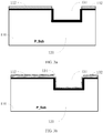
FIGS. 3a to 3d are a cross-sectional structural schematic views of a semiconductor device during a manufacturing process by the method shown inFIG. 2 . - In order to facilitate the understanding of the present disclosure, the present disclosure will be described more fully below with reference to relevant attached drawings. Preferred embodiments of the present disclosure are illustrated in the drawings. However, the present disclosure can be implemented in many different forms and is not limited to the embodiments described herein. On the contrary, providing these embodiments is to assist understanding the content disclosed by the present disclosure more fully and thoroughly.
- Unless otherwise defined, all technical and scientific terms used herein have the same meaning as commonly understood by those skilled in the technical field of the present disclosure. The terms used in the specification of the present disclosure herein are only for the purpose of describing specific embodiments, and are not intended to limit the present disclosure. The term "and/or" as used herein includes any and all combinations of one or more related listed items.
- Terms related to a semiconductor field used herein are technical terms commonly used by those skilled in the art. For example, for P type and N type impurities, in order to distinguish a doping concentration, a P+ type simply represents a P type with heavy doping concentration, a P type represents a P type with medium doping concentration, a P- type represents a P type with light doping concentration, a N+ type represents a N type with heavy doping concentration, a N type represents a N type with medium doping concentration, and a N- type represents a N type with light doping concentration.
-
FIG. 1 is a cross-sectional structural schematic view of a semiconductor device according to an embodiment. The semiconductor device includes adrift region 120, anisolation structure 130, and ahole field plate 180. Theisolation structure 130 is in contact with thedrift region 120. Theisolation structure 130 includes afirst isolation layer 132, a holeetch stop layer 134 formed on thefirst isolation layer 132, and asecond isolation layer 136 formed on the holeetch stop layer 134. Thehole field plate 180 is disposed above the holeetch stop layer 134 and is in contact with the holeetch stop layer 134. In the embodiment shown inFIG. 1 , thedrift region 120 surrounds theisolation structure 130 in a cross section, and thehole field plate 180 extends downward to the holeetch stop layer 134. - The aforementioned semiconductor device has the
hole field plate 180 connected to theisolation structure 130. Since theisolation structure 130 is in contact with thedrift region 120, thehole field plate 180 can help to deplete thedrift region 120, thereby effectively improving the breakdown voltage of the device. The holeetch stop layer 134 is formed in theisolation structure 130, such that thehole field plate 180 can be accurately controlled to extend downward to a position of the holeetch stop layer 134, and a thickness of theisolation structure 130 below thehole field plate 180 can be controlled to be a thickness of thefirst isolation layer 132, thereby ensuring that the effect of thehole field plate 180 helping to deplete thedrift region 120 will not deviate from an expectation due to thehole field plate 180 being too deep or too shallow (that is, the depth of the holes deviating from a design value). Therefore, the stability and uniformity of the device can be guaranteed. - The
isolation structure 130 adds the holeetch stop layer 134 made of another material inside the conventional isolation structure. That is, inside the isolation structure made of an insulating material A, the hole etch stop layer made of a material B is added. It is necessary that there is a higher etching selectivity between the material B and the insulating material A, such that when forming (holes of) thehole field plate 180 by etching, the etching will stop at the holeetch stop layer 134 after etching through thesecond isolation layer 136. - In order to prevent the hole
etch stop layer 134 from affecting the performance of theisolation structure 130 itself, the holeetch stop layer 134 should be made relatively thin. Of course, the premise is to ensure that when thehole field plate 180 is formed by etching, the etching will not etch through the holeetch stop layer 134 within a reasonable etching time. - In one embodiment, the
isolation structure 130 is a shallow trench isolation structure (STI). Thefirst isolation layer 132 and thesecond isolation layer 136 are made of silicon oxide, such as silicon dioxide. - In one embodiment, the hole
etch stop layer 134 is made of a nitrogen-containing compound, such as silicon nitride. - In one embodiment, the
hole field plate 180 is made of an insulating material. That is, the material filled in the holes is an insulating material. - In one embodiment, the semiconductor device further includes a metal layer (not shown in
FIG. 1 ). A top portion of thehole field plate 180 is connected to the metal layer. In one embodiment, the semiconductor device further includes an interlayer dielectric (ILD) 190 disposed between theisolation structure 130 and the metal layer. Thehole field plate 180 extends through the interlayer dielectric 190 to connect the metal layer and theisolation structure 130. - The interlayer dielectric 190 may be made of a material used as an interlayer dielectric known in the art, such as phosphosilicate glass (PSG), or borophosphosilicate glass (BPSG).
- In one embodiment, the semiconductor device further includes a
polysilicon structure 174. Thepolysilicon structure 174 includes a polysilicon gate located on agate oxide layer 172 and a polysilicon field plate extending to theisolation structure 130. - In one embodiment, the semiconductor device is a lateral diffusion metal oxide semiconductor field effect transistor (LDMOSFET).
- In the embodiment shown in
FIG. 1 , the semiconductor device includes adrain region 142 and asource region 162. The polysilicon gate is located above a region between thedrain region 142 and thesource region 162. The drainregion 142 is located in thedrift region 120, and thedrain region 142 is located at a side of theisolation structure 130 opposite to the polysilicon gate (inFIG. 1 , thedrain region 142 is located on the right side of theisolation structure 130, and the polysilicon gate is located on the left side of the isolation structure 130). - In the embodiment shown in
FIG. 1 , thedrift region 120 of a first conductivity type is located in asubstrate 110 of a second conductivity type. The semiconductor device further includes awell region 150 of the second conductivity type formed in thesubstrate 110. A side of the polysilicon gate opposite to theisolation structure 130 extends onto thewell region 150 of the second conductive type. - In the embodiment shown in
FIG. 1 , the semiconductor device further includes adoped region 164 of the second conductivity type located in thewell region 150 of the second conductivity type. Thedoped region 164 of the second conductivity type is located at a side of thesource region 162 away from the polysilicon gate. - In the embodiment shown in
FIG. 1 , the holes of thehole field plate 180 are contact holes (CT). - In one embodiment, the first conductivity type is the N type and the second conductivity type is the P type. In the embodiment shown in
FIG. 1 , thesubstrate 110 is a P type substrate (P_Sub), thedrift region 120 is an N type drift region (N_Drift). Thewell region 150 of the second conductivity type is a P well (PW). Thedrain region 142 is an N+ drain region. Thesource region 162 is an N+ source region. The dopedregion 164 of the second conductivity type is a P+ region. - In other embodiments, the first conductivity type may be a P type, and the second conductivity type may be an N type.
- The present application also provides a method for manufacturing a semiconductor device, which can be used to manufacture the semiconductor device of any of the above embodiments.
FIG. 2 is a flowchart of a method for manufacturing a semiconductor device in an embodiment. The method includes the following steps. - S210, a trench is formed on a surface of a substrate.
- The trench is formed to form an isolation structure in the trench. In one embodiment, the trench may be formed by an etching process.
- Referring to
FIG. 3a , in one embodiment, ahard mask 112 is used as a mask to etch atrench 131. For example, using silicon nitride as thehard mask 112, an etching window where thetrench 131 is to be formed is exposed by photolithography, and then the silicon nitride at the etching window is etched away, and thetrench 131 is formed by etching downward. - S220, a first isolation layer is formed on an inner surface of the trench.
- Referring to
FIG. 3a , in this embodiment, afirst isolation layer 132 is made of silicon oxide, such as silicon dioxide. In the embodiment shown inFIG. 3a , this step includes growing a layer of oxide on thesubstrate 110 by thermal oxidation. In the embodiment shown inFIG. 3a , thefirst isolation layer 132 is also grown below thehard mask 112. - S230, a hole etch stop layer is formed on the first isolation layer.
- Referring to
FIG. 3b , in one embodiment, a holeetch stop layer 134 is formed by a deposition process. For ease of operation, the deposited holeetch stop layer 134 in the embodiment shown inFIG. 3b is also formed on thehard mask 112. - S240, a second isolation layer is forming at a remaining region in the trench.
- In order to ensure that the trench is fully filled, in the embodiment shown in
FIG. 3c , asecond isolation layer 136 is over-deposited. That is, the thickness of the depositedsecond isolation layer 136 is greater than the thickness required to fill the trench. The formedsecond isolation layer 136 covers the holeetch stop layer 134 in the trench and the holeetch stop layer 134 outside the trench. Thefirst isolation layer 132, the holeetch stop layer 134 and thesecond isolation layer 136 cooperatively form an isolation structure. - In the embodiment shown in
FIG. 3d , after step S240 is completed, the surface of the substrate is planarized. For example, a portion of thefirst isolation layer 132 is removed using chemical mechanical polishing (CMP). Then, thehard mask 112, thesecond isolation layer 136, the holeetch stop layer 134, and thefirst isolation layer 132 on thesubstrate 110 are peeled off (by an etching process, without etching away the isolation structure in the trench). Finally, a structure shown inFIG. 3d is obtained. - S250, a drift region is formed.
- The drift region is in contact with the isolation structure. In this embodiment, the drift region is formed after the isolation structure is formed (that is, after the
first isolation layer 132, the holeetch stop layer 134, and thesecond isolation layer 136 are formed). In other embodiments, the drift region may also be firstly formed, and then the isolation structure is formed. - S260, a field plate hole is formed by etching.
- When etching the field plate hole, depths of the holes are controlled by the hole
etch stop layer 134. Therefore, it is necessary that there is a higher etching selectivity between a material forming the holeetch stop layer 134 and a material forming thesecond isolation layer 136, such that the etching will stop at the holeetch stop layer 134 after etching through thesecond isolation layer 136. In one embodiment, thesecond isolation layer 136 is made of silicon oxide, such as silicon dioxide. The holeetch stop layer 134 is made of a nitrogen-containing compound, such as silicon nitride. - S270, a material is filled into the field plate hole to form a hole field plate.
- The above semiconductor device is formed with the hole field plate connected to the isolation structure. Since the isolation structure is in contact with the drift region, the hole field plate can help to deplete the drift region, thereby effectively improving the breakdown voltage of the device. The hole
etch stop layer 134 is formed in the isolation structure, such that a position to which the hole field plate extends downward can be accurately controlled, and the thickness of the isolation structure below the hole field plate can be controlled to be the thickness of thefirst isolation layer 132, thereby ensuring that the effect of the hole field plate helping to deplete the drift region will not deviate from an expectation due to the hole field plate being too deep or too shallow (that is, the depth of the hole deviating from a design value). Therefore, the stability and uniformity of the device can be guaranteed. - Since the depletion effect of the hole field plate to the drift region is related to the thickness of the isolation structure below the hole field plate, the required thickness of the
first isolation layer 132 can be pre-calculated according to the required breakdown voltage of the device (or the required thickness of thefirst isolation layer 132 is pre-calculated by other means). In step S220, silicon oxide is grown according to the thickness. In addition, the holeetch stop layer 134 formed in step S230 is used to separate thefirst isolation layer 132 from thesecond isolation layer 136, such that the required thickness of thefirst isolation layer 132 can be predetermined, thus further effectively controlling the thickness of thefirst isolation layer 132. - In one embodiment, the semiconductor device is a lateral diffusion metal oxide semiconductor field effect transistor (LDMOSFET).
- In one embodiment, after step S240, processes such as well implantation, gate oxidation, polysilicon deposition, source/drain implantation are further included. It should be understood that these steps can be performed by methods known in the art.
- In one embodiment, a step of forming an interlayer dielectric on the isolation structure is further included. In step S260, after etching through the interlayer dielectric, continue to etch the
second isolation layer 136 downward to the holeetch stop layer 134. In one embodiment, after forming the interlayer dielectric on the isolation structure, a step of forming a metal layer on the interlayer dielectric is further included. The top portion of the hole field plate is connected to the metal layer. - The interlayer dielectric may be made of a material used as an interlayer dielectric known in the art, such as phosphosilicate glass (PSG), or borophosphosilicate glass (BPSG).
- In order to prevent the hole
etch stop layer 134 from affecting the performance of the isolation structure itself, the holeetch stop layer 134 should be made relatively thin in step S230. Of course, the premise is to ensure that when the etching time in step S230 is within a reasonable range, the holeetch stop layer 134 will not be etched through. - Only several implementations of the present disclosure are illustrated in the aforementioned embodiments, and the description thereof is relatively specific and detailed, but it should not be understood as a limitation on the scope of the present disclosure. It should be noted that for those of ordinary skill in the art, without departing from the concept of the present disclosure, several modifications and improvements can be made, which all fall within the protection scope of the present disclosure. Therefore, the protection scope of the present disclosure shall be subject to the appended claims.
Claims (15)
- A semiconductor device, comprising:a drift region;an isolation structure in contact with the drift region, the isolation structure comprising a first isolation layer, a hole etch stop layer formed on the first isolation layer, and a second isolation layer formed on the hole etch stop layer; anda hole field plate disposed above the hole etch stop layer and in contact with the hole etch stop layer.
- The semiconductor device according to claim 1, wherein the isolation structure is a shallow trench isolation structure, the first isolation layer and the second isolation layer are made of silicon oxide.
- The semiconductor device according to claim 2, wherein the hole etch stop layer is made of a nitrogen-containing compound.
- The semiconductor device according to claim 1, wherein the hole field plate is made of an insulating material.
- The semiconductor device according to claim 1, further comprising a metal layer, wherein a top portion of the hole field plate is connected to the metal layer.
- The semiconductor device according to claim 5, further comprising an interlayer dielectric disposed between the isolation structure and the metal layer, wherein the hole field plate extends through the interlayer dielectric to connect the metal layer and the isolation structure.
- The semiconductor device according to claim 1, further comprising a polysilicon structure comprising a polysilicon gate and a polysilicon field plate.
- The semiconductor device according to claim 7, wherein the semiconductor device is a lateral diffusion metal oxide semiconductor field effect transistor.
- The semiconductor device according to claim 8, further comprising a drain region and a source region, wherein the polysilicon gate is located above a region between the drain region and the source region, the drain region is located in the drift region, and the drain region is located at a side of the isolation structure opposite to the polysilicon gate.
- The semiconductor device according to claim 9, further comprising a substrate of a second conductivity type and a well region of the second conductivity type formed in the substrate, wherein a side of the polysilicon gate opposite to the isolation structure extends onto the well region of the second conductive type, the drift region is of a first conductivity type, and the drift region is located in the substrate.
- The semiconductor device according to claim 10, further comprising a doped region of the second conductivity type located in the well region of the second conductivity type, the doped region of the second conductivity type being located at a side of the source region away from the polysilicon gate.
- The semiconductor device according to claim 10, wherein the first conductivity type is a N type, and the second conductivity type is a P type.
- A method for manufacturing a semiconductor device, comprising:forming a trench on a surface of a substrate;forming a first isolation layer on an inner surface of the trench;forming a hole etch stop layer on the first isolation layer;forming a second isolation layer at a remaining region in the trench;forming a drift region, wherein the drift region is in contact with an isolation structure, andthe isolation structure comprises the first isolation layer, the hole etch stop layer, and the second isolation layer;forming a field plate hole by etching, the field plate hole extending through the second isolation layer to the hole etch stop layer; andfilling a material into the field plate hole to form a hole field plate.
- The method according to claim 13, further comprising a step of forming an interlayer dielectric on the isolation structure, wherein the step of forming the field plate hole by etching comprises: after etching through the interlayer dielectric, continuing to etch the second isolation layer downward to the hole etch stop layer.
- The method according to claim 13, wherein the step of forming the first isolation layer on the inner surface of the trench comprises: thermally growing a silicon oxide.
Applications Claiming Priority (2)
| Application Number | Priority Date | Filing Date | Title |
|---|---|---|---|
| CN201810840983.8A CN110767740B (en) | 2018-07-27 | 2018-07-27 | Semiconductor device and method of manufacturing the same |
| PCT/CN2019/097836 WO2020020328A1 (en) | 2018-07-27 | 2019-07-26 | Semiconductor device and method for manufacturing same |
Publications (2)
| Publication Number | Publication Date |
|---|---|
| EP3832733A1 true EP3832733A1 (en) | 2021-06-09 |
| EP3832733A4 EP3832733A4 (en) | 2022-04-20 |
Family
ID=69180780
Family Applications (1)
| Application Number | Title | Priority Date | Filing Date |
|---|---|---|---|
| EP19841203.3A Pending EP3832733A4 (en) | 2018-07-27 | 2019-07-26 | SEMICONDUCTOR DEVICE AND METHOD FOR MAKING IT |
Country Status (6)
| Country | Link |
|---|---|
| US (1) | US11588049B2 (en) |
| EP (1) | EP3832733A4 (en) |
| JP (1) | JP7145313B2 (en) |
| KR (1) | KR102520058B1 (en) |
| CN (1) | CN110767740B (en) |
| WO (1) | WO2020020328A1 (en) |
Families Citing this family (6)
| Publication number | Priority date | Publication date | Assignee | Title |
|---|---|---|---|---|
| CN114335163B (en) * | 2020-09-30 | 2025-03-25 | 芯恩(青岛)集成电路有限公司 | LDMOS transistor with vertical floating field plate and method for manufacturing the same |
| CN120751736A (en) | 2021-04-12 | 2025-10-03 | 联华电子股份有限公司 | Laterally diffused metal oxide semiconductor element and manufacturing method thereof |
| TWI792495B (en) * | 2021-08-16 | 2023-02-11 | 立錡科技股份有限公司 | Power device and manufacturing method thereof |
| US20240162345A1 (en) * | 2022-11-10 | 2024-05-16 | Globalfoundries U.S. Inc. | Transistor with metal field plate contact |
| CN116978788A (en) * | 2023-09-25 | 2023-10-31 | 粤芯半导体技术股份有限公司 | LDMOS device with multilayer field plate structure and preparation method thereof |
| US12289913B1 (en) * | 2024-04-22 | 2025-04-29 | Globalfoundries Singapore Pte. Ltd | Device with metal field plate extension |
Family Cites Families (23)
| Publication number | Priority date | Publication date | Assignee | Title |
|---|---|---|---|---|
| JPH07135249A (en) * | 1993-11-09 | 1995-05-23 | Matsushita Electric Ind Co Ltd | Semiconductor device and manufacturing method thereof |
| TW466747B (en) * | 2000-12-14 | 2001-12-01 | United Microelectronics Corp | Using inner field ring and complex multiple field plates to reduce surface breakdown of power LDMOSFET |
| JP2003332424A (en) * | 2002-05-14 | 2003-11-21 | Sharp Corp | Method for manufacturing semiconductor device |
| US7118987B2 (en) * | 2004-01-29 | 2006-10-10 | Taiwan Semiconductor Manufacturing Co., Ltd. | Method of achieving improved STI gap fill with reduced stress |
| JP2005303253A (en) * | 2004-03-18 | 2005-10-27 | Fuji Electric Device Technology Co Ltd | Manufacturing method of semiconductor device |
| US8134208B2 (en) * | 2007-09-26 | 2012-03-13 | Globalfoundries Inc. | Semiconductor device having decreased contact resistance |
| US7956412B2 (en) | 2007-12-04 | 2011-06-07 | International Business Machines Corporation | Lateral diffusion field effect transistor with a trench field plate |
| JP5486498B2 (en) * | 2008-08-01 | 2014-05-07 | ルネサスエレクトロニクス株式会社 | Semiconductor device and manufacturing method of semiconductor device |
| JP4602465B2 (en) * | 2008-12-04 | 2010-12-22 | 株式会社東芝 | Semiconductor device |
| US20110115018A1 (en) * | 2009-11-13 | 2011-05-19 | Maxim Integrated Products, Inc. | Mos power transistor |
| JP2011171638A (en) * | 2010-02-22 | 2011-09-01 | Oki Semiconductor Co Ltd | Method of manufacturing semiconductor device |
| US8981475B2 (en) | 2013-06-18 | 2015-03-17 | International Business Machines Corporation | Lateral diffusion metal oxide semiconductor (LDMOS) |
| JP6279346B2 (en) * | 2014-02-27 | 2018-02-14 | ルネサスエレクトロニクス株式会社 | Semiconductor device |
| DE102014206361A1 (en) * | 2014-04-03 | 2015-10-08 | Robert Bosch Gmbh | A method of fabricating a dielectric field plate in a trench of a substrate, a substrate obtainable by the method, and a power transistor having such a substrate |
| US9842903B2 (en) * | 2014-10-20 | 2017-12-12 | Globalfoundries Singapore Pte. Ltd. | Integrated circuits with laterally diffused metal oxide semiconductor structures and methods for fabricating the same |
| CN104538309A (en) * | 2014-12-31 | 2015-04-22 | 上海华虹宏力半导体制造有限公司 | Low on resistance LDMOS structure and manufacturing method thereof |
| CN104992977B (en) * | 2015-05-25 | 2018-06-19 | 上海华虹宏力半导体制造有限公司 | NLDMOS device and its manufacturing method |
| JP6509665B2 (en) * | 2015-07-23 | 2019-05-08 | ルネサスエレクトロニクス株式会社 | Semiconductor device |
| DE102015112427B4 (en) | 2015-07-29 | 2017-04-06 | Infineon Technologies Ag | A semiconductor device having a gradually increasing field dielectric layer and method of manufacturing a semiconductor device |
| CN106549052B (en) * | 2015-09-17 | 2021-05-25 | 联华电子股份有限公司 | Laterally diffused metal oxide semiconductor transistor and method of making the same |
| KR102286013B1 (en) * | 2015-10-07 | 2021-08-05 | 에스케이하이닉스 시스템아이씨 주식회사 | Lateral high voltage integrated device having tranch insulating field plate and metal field plate |
| US10804389B2 (en) * | 2016-02-25 | 2020-10-13 | Taiwan Semiconductor Manufacturing Company, Ltd. | LDMOS transistor |
| US11411086B2 (en) * | 2020-03-17 | 2022-08-09 | Taiwan Semiconductor Manufacturing Company, Ltd. | Field plate and isolation structure for high voltage device |
-
2018
- 2018-07-27 CN CN201810840983.8A patent/CN110767740B/en active Active
-
2019
- 2019-07-26 EP EP19841203.3A patent/EP3832733A4/en active Pending
- 2019-07-26 WO PCT/CN2019/097836 patent/WO2020020328A1/en not_active Ceased
- 2019-07-26 KR KR1020217005241A patent/KR102520058B1/en active Active
- 2019-07-26 US US17/262,882 patent/US11588049B2/en active Active
- 2019-07-26 JP JP2021504447A patent/JP7145313B2/en active Active
Also Published As
| Publication number | Publication date |
|---|---|
| CN110767740B (en) | 2021-10-15 |
| EP3832733A4 (en) | 2022-04-20 |
| US20210234041A1 (en) | 2021-07-29 |
| WO2020020328A1 (en) | 2020-01-30 |
| JP7145313B2 (en) | 2022-09-30 |
| KR102520058B1 (en) | 2023-04-10 |
| KR20210034650A (en) | 2021-03-30 |
| CN110767740A (en) | 2020-02-07 |
| US11588049B2 (en) | 2023-02-21 |
| JP2021532594A (en) | 2021-11-25 |
Similar Documents
| Publication | Publication Date | Title |
|---|---|---|
| TWI668744B (en) | Semiconductor devices and methods for forming the same | |
| US11588049B2 (en) | Semiconductor device and method for manufacturing same | |
| US20210272849A1 (en) | Wrap-Around Contact on FinFET | |
| US10998315B2 (en) | Metal gate modulation to improve kink effect | |
| TWI705503B (en) | Semiconductor structure and associated fabricating method | |
| US8629008B2 (en) | Electrical isolation structures for ultra-thin semiconductor-on-insulator devices | |
| US8642459B2 (en) | Method for forming a semiconductor device with an isolation region on a gate electrode | |
| KR102202818B1 (en) | Transistor layout to reduce kink effect | |
| US10043804B2 (en) | LDMOS design for a FinFET device | |
| US8835264B1 (en) | Method for fabricating power semiconductor device | |
| US11316043B2 (en) | Semiconductor transistor device and method of manufacturing the same | |
| US11961907B2 (en) | Laterally-diffused metal-oxide semiconductor transistor and method therefor | |
| TWI485783B (en) | Semiconductor device having packaged pressure source region and manufacturing method thereof | |
| KR20070020919A (en) | Recess channel array transistor and method of manufacturing same | |
| US20250372447A1 (en) | Semiconductor devices with air gap and multiple implant steps for sealing the air gap | |
| KR20050069662A (en) | A manufacturing method of layer insulation film of semiconductor element |
Legal Events
| Date | Code | Title | Description |
|---|---|---|---|
| STAA | Information on the status of an ep patent application or granted ep patent |
Free format text: STATUS: THE INTERNATIONAL PUBLICATION HAS BEEN MADE |
|
| PUAI | Public reference made under article 153(3) epc to a published international application that has entered the european phase |
Free format text: ORIGINAL CODE: 0009012 |
|
| STAA | Information on the status of an ep patent application or granted ep patent |
Free format text: STATUS: REQUEST FOR EXAMINATION WAS MADE |
|
| 17P | Request for examination filed |
Effective date: 20210119 |
|
| AK | Designated contracting states |
Kind code of ref document: A1 Designated state(s): AL AT BE BG CH CY CZ DE DK EE ES FI FR GB GR HR HU IE IS IT LI LT LU LV MC MK MT NL NO PL PT RO RS SE SI SK SM TR |
|
| DAV | Request for validation of the european patent (deleted) | ||
| DAX | Request for extension of the european patent (deleted) | ||
| A4 | Supplementary search report drawn up and despatched |
Effective date: 20220321 |
|
| RIC1 | Information provided on ipc code assigned before grant |
Ipc: H01L 29/78 20060101ALI20220315BHEP Ipc: H01L 21/336 20060101ALI20220315BHEP Ipc: H01L 29/06 20060101ALI20220315BHEP Ipc: H01L 29/40 20060101AFI20220315BHEP |