EP3832717A1 - Monolithic back-to-back isolation elements with floating top plate - Google Patents
Monolithic back-to-back isolation elements with floating top plate Download PDFInfo
- Publication number
- EP3832717A1 EP3832717A1 EP20209202.9A EP20209202A EP3832717A1 EP 3832717 A1 EP3832717 A1 EP 3832717A1 EP 20209202 A EP20209202 A EP 20209202A EP 3832717 A1 EP3832717 A1 EP 3832717A1
- Authority
- EP
- European Patent Office
- Prior art keywords
- isolator
- component
- isolator component
- components
- integrated
- Prior art date
- Legal status (The legal status is an assumption and is not a legal conclusion. Google has not performed a legal analysis and makes no representation as to the accuracy of the status listed.)
- Granted
Links
Images




Classifications
-
- H—ELECTRICITY
- H05—ELECTRIC TECHNIQUES NOT OTHERWISE PROVIDED FOR
- H05K—PRINTED CIRCUITS; CASINGS OR CONSTRUCTIONAL DETAILS OF ELECTRIC APPARATUS; MANUFACTURE OF ASSEMBLAGES OF ELECTRICAL COMPONENTS
- H05K1/00—Printed circuits
- H05K1/02—Details
- H05K1/0213—Electrical arrangements not otherwise provided for
- H05K1/0216—Reduction of cross-talk, noise or electromagnetic interference
- H05K1/023—Reduction of cross-talk, noise or electromagnetic interference using auxiliary mounted passive components or auxiliary substances
-
- H—ELECTRICITY
- H10—SEMICONDUCTOR DEVICES; ELECTRIC SOLID-STATE DEVICES NOT OTHERWISE PROVIDED FOR
- H10D—INORGANIC ELECTRIC SEMICONDUCTOR DEVICES
- H10D62/00—Semiconductor bodies, or regions thereof, of devices having potential barriers
- H10D62/10—Shapes, relative sizes or dispositions of the regions of the semiconductor bodies; Shapes of the semiconductor bodies
- H10D62/113—Isolations within a component, i.e. internal isolations
- H10D62/115—Dielectric isolations, e.g. air gaps
-
- H—ELECTRICITY
- H10—SEMICONDUCTOR DEVICES; ELECTRIC SOLID-STATE DEVICES NOT OTHERWISE PROVIDED FOR
- H10W—GENERIC PACKAGES, INTERCONNECTIONS, CONNECTORS OR OTHER CONSTRUCTIONAL DETAILS OF DEVICES COVERED BY CLASS H10
- H10W20/00—Interconnections in chips, wafers or substrates
- H10W20/40—Interconnections external to wafers or substrates, e.g. back-end-of-line [BEOL] metallisations or vias connecting to gate electrodes
- H10W20/495—Capacitive arrangements or effects of, or between wiring layers
- H10W20/496—Capacitor integral with wiring layers
-
- H—ELECTRICITY
- H10—SEMICONDUCTOR DEVICES; ELECTRIC SOLID-STATE DEVICES NOT OTHERWISE PROVIDED FOR
- H10W—GENERIC PACKAGES, INTERCONNECTIONS, CONNECTORS OR OTHER CONSTRUCTIONAL DETAILS OF DEVICES COVERED BY CLASS H10
- H10W20/00—Interconnections in chips, wafers or substrates
- H10W20/40—Interconnections external to wafers or substrates, e.g. back-end-of-line [BEOL] metallisations or vias connecting to gate electrodes
- H10W20/497—Inductive arrangements or effects of, or between, wiring layers
-
- H—ELECTRICITY
- H10—SEMICONDUCTOR DEVICES; ELECTRIC SOLID-STATE DEVICES NOT OTHERWISE PROVIDED FOR
- H10W—GENERIC PACKAGES, INTERCONNECTIONS, CONNECTORS OR OTHER CONSTRUCTIONAL DETAILS OF DEVICES COVERED BY CLASS H10
- H10W70/00—Package substrates; Interposers; Redistribution layers [RDL]
- H10W70/40—Leadframes
- H10W70/475—Capacitors in combination with leadframes
-
- H—ELECTRICITY
- H10—SEMICONDUCTOR DEVICES; ELECTRIC SOLID-STATE DEVICES NOT OTHERWISE PROVIDED FOR
- H10W—GENERIC PACKAGES, INTERCONNECTIONS, CONNECTORS OR OTHER CONSTRUCTIONAL DETAILS OF DEVICES COVERED BY CLASS H10
- H10W72/00—Interconnections or connectors in packages
- H10W72/071—Connecting or disconnecting
- H10W72/075—Connecting or disconnecting of bond wires
- H10W72/07551—Connecting or disconnecting of bond wires characterised by changes in properties of the bond wires during the connecting
- H10W72/07552—Connecting or disconnecting of bond wires characterised by changes in properties of the bond wires during the connecting changes in structures or sizes
-
- H—ELECTRICITY
- H10—SEMICONDUCTOR DEVICES; ELECTRIC SOLID-STATE DEVICES NOT OTHERWISE PROVIDED FOR
- H10W—GENERIC PACKAGES, INTERCONNECTIONS, CONNECTORS OR OTHER CONSTRUCTIONAL DETAILS OF DEVICES COVERED BY CLASS H10
- H10W72/00—Interconnections or connectors in packages
- H10W72/50—Bond wires
- H10W72/521—Structures or relative sizes of bond wires
- H10W72/527—Multiple bond wires having different sizes
-
- H—ELECTRICITY
- H10—SEMICONDUCTOR DEVICES; ELECTRIC SOLID-STATE DEVICES NOT OTHERWISE PROVIDED FOR
- H10W—GENERIC PACKAGES, INTERCONNECTIONS, CONNECTORS OR OTHER CONSTRUCTIONAL DETAILS OF DEVICES COVERED BY CLASS H10
- H10W72/00—Interconnections or connectors in packages
- H10W72/50—Bond wires
- H10W72/531—Shapes of wire connectors
- H10W72/536—Shapes of wire connectors the connected ends being ball-shaped
-
- H—ELECTRICITY
- H10—SEMICONDUCTOR DEVICES; ELECTRIC SOLID-STATE DEVICES NOT OTHERWISE PROVIDED FOR
- H10W—GENERIC PACKAGES, INTERCONNECTIONS, CONNECTORS OR OTHER CONSTRUCTIONAL DETAILS OF DEVICES COVERED BY CLASS H10
- H10W72/00—Interconnections or connectors in packages
- H10W72/50—Bond wires
- H10W72/541—Dispositions of bond wires
- H10W72/5453—Dispositions of bond wires connecting between multiple bond pads on a chip, e.g. daisy chain
-
- H—ELECTRICITY
- H10—SEMICONDUCTOR DEVICES; ELECTRIC SOLID-STATE DEVICES NOT OTHERWISE PROVIDED FOR
- H10W—GENERIC PACKAGES, INTERCONNECTIONS, CONNECTORS OR OTHER CONSTRUCTIONAL DETAILS OF DEVICES COVERED BY CLASS H10
- H10W72/00—Interconnections or connectors in packages
- H10W72/90—Bond pads, in general
- H10W72/981—Auxiliary members, e.g. spacers
- H10W72/983—Reinforcing structures, e.g. collars
-
- H—ELECTRICITY
- H10—SEMICONDUCTOR DEVICES; ELECTRIC SOLID-STATE DEVICES NOT OTHERWISE PROVIDED FOR
- H10W—GENERIC PACKAGES, INTERCONNECTIONS, CONNECTORS OR OTHER CONSTRUCTIONAL DETAILS OF DEVICES COVERED BY CLASS H10
- H10W90/00—Package configurations
- H10W90/701—Package configurations characterised by the relative positions of pads or connectors relative to package parts
- H10W90/751—Package configurations characterised by the relative positions of pads or connectors relative to package parts of bond wires
- H10W90/753—Package configurations characterised by the relative positions of pads or connectors relative to package parts of bond wires between laterally-adjacent chips
-
- H—ELECTRICITY
- H10—SEMICONDUCTOR DEVICES; ELECTRIC SOLID-STATE DEVICES NOT OTHERWISE PROVIDED FOR
- H10W—GENERIC PACKAGES, INTERCONNECTIONS, CONNECTORS OR OTHER CONSTRUCTIONAL DETAILS OF DEVICES COVERED BY CLASS H10
- H10W90/00—Package configurations
- H10W90/701—Package configurations characterised by the relative positions of pads or connectors relative to package parts
- H10W90/751—Package configurations characterised by the relative positions of pads or connectors relative to package parts of bond wires
- H10W90/756—Package configurations characterised by the relative positions of pads or connectors relative to package parts of bond wires between a chip and a stacked lead frame, conducting package substrate or heat sink
Definitions
- the present application relates to galvanic isolators providing galvanic isolation between circuits.
- Isolators provide electrical isolation between circuits which communicate with each other. In some situations, circuits which communicate with each other operate at different voltages, for instance one at a relatively high voltage and the other at a relatively low voltage. In some situations, the circuits are referenced to different electrical ground potentials. Isolators can be used to electrically isolate circuits in either of these situations. Connecting multiple isolators in series may increase the amount of isolation between the circuits.
- Isolators having a back-to-back configuration for providing electrical isolation between two circuits are described, in which multiple isolators formed on a single, monolithic substrate are connected in series to achieve a higher amount of electrical isolation for a single substrate than for a single isolator formed on substrate. Connecting the top isolator components, which are distal from the single substrate, may provide electrical isolation to the top isolator components.
- the back-to-back isolator may provide one or more communication channels for transfer of information and/or power between the circuits connected to the bottom isolator components.
- an integrated isolator device comprises a substrate, and a first isolator component and a second isolator component positioned over the substrate.
- the integrated isolator device further comprises a third isolator component positioned over the first isolator component and a fourth isolator component positioned over the second isolator component.
- the integrated isolator device further comprises at least one conductor connecting the third isolator component to the fourth isolator component.
- an integrated isolator device comprises a substrate, and a first isolator component and a second isolator component positioned over the substrate.
- the integrated isolator device further comprises at least one third isolator component configured to electromagnetically couple with the first isolator component and the second isolator component.
- the first isolator component and the second isolator component are positioned between the at least one third isolator component and the substrate.
- the integrated isolator device further comprises a first electrical contact coupled to the first isolator component and a second electrical contact coupled to the second isolator component.
- a system comprising an isolator, at least one first circuit, and at least one second circuit.
- the isolator comprises a substrate, and a first isolator component and a second isolator component positioned over the substrate.
- the isolator further comprises at least one third isolator component positioned over the first isolator component and the second isolator component.
- the at least one first circuit is coupled to the first isolator component and configured to operate in a first voltage domain.
- the at least one second circuit coupled to the second isolator component and configured to operate in a second voltage domain different than the first voltage domain.
- aspects of the present application relate to a back-to-back isolator formed on a single monolithic integrated device.
- the back-to-back isolator includes two or more isolators connected in series formed on a single substrate (e.g ., glass substrate, ceramic substrate, semiconductor substrate).
- a single substrate e.g ., glass substrate, ceramic substrate, semiconductor substrate.
- One approach for achieving a back-to-back configuration is to connect two isolators on separate substrates in series to achieve an effective isolation equaling the cumulative isolation properties of the two isolators.
- aspects of the present application provide back-to-back isolators formed on a single substrate.
- a benefit of a monolithic configuration is that the total isolation may be the cumulative isolation properties of two isolators, with less overall footprint (substrate area) because the structure has substantially similar area as a single isolator (e.g ., approximately 10%-15% larger than a single isolator). For example, if each isolator in the back-to-back configuration can withstand 600 V, then the cumulative isolation the back-to-back isolator can handle is approximately 1200 V. Additionally, forming the back-to-back isolator on a single substrate reduces costs in comparison to a multi-substrate back-to-back configuration because less substrate area is used.
- the higher isolation provided by the back-to-back isolator on a single substrate can be implemented in high voltage applications, such as industrial (e.g ., machine monitoring) and healthcare or medical applications, which typically require high isolation voltages-for example, the ability to protect against surge events (e.g ., 15kV - 20kV)-that can be challenging to achieve with single isolators. More generally, it may be desirable to isolate voltages from approximately 400V up to approximately 20kV, whether in steady state operation or as surge events.
- aspects of the present application relate to a back-to-back isolator structure that includes a first pair of isolator components (e.g., coils or windings, or capacitive plates) forming one of the isolators and a second pair of isolator components forming the other isolator.
- the isolator components in each pair are arranged vertically within the integrated device, forming a top isolator component and a bottom isolator component at different vertical levels separated by dielectric material.
- the top isolator components are electrically shorted together and are electrically isolated from the underlying substrate and the bottom isolator components, forming floating top isolator components in the integrated device.
- the bottom isolator components are configured to act as inputs and outputs for the back-to-back isolator.
- a bottom isolator component of the first pair may electrically connect to a transmitter while a bottom isolator component of the second pair may electrically connect to a receiver.
- the capacitance between the isolator components of a pair is high to allow for electric field coupling or magnetic field coupling.
- parasitic capacitance may exist between the floating isolator components and an underlying conductor.
- the isolator may be disposed on a paddle portion of a lead frame as part of packaging for the isolator.
- a parasitic capacitance may exist between the floating isolator components and the paddle portion.
- the parasitic capacitance between the floating isolator components and an underlying conductor may reduce the voltage capabilities that the isolator may otherwise be configured to achieve.
- the parasitic capacitance may result in a voltage imbalance between the two isolators in the back-to-back configuration and, during operation, the resulting isolator may be limited by the device connected to the isolator having the higher portion of the voltage.
- the back-to-back configuration described in the present application may provide the benefit of reducing or eliminating parasitic capacitance between the top isolator components and an underlying conductor, such as the underlying substrate (e.g ., silicon substrate) and/or a paddle portion of the lead frame that the isolator is positioned on as part of packaging for the isolator.
- floating the top isolator components increases the thickness of the dielectric material between the floating isolator components and the underlying conductor, which may reduce or eliminate the parasitic capacitance.
- the back-to-back isolator may be formed on a microfabricated substrate (e.g ., glass substrate, silicon substrate) having a substantial thickness of dielectric material (e.g., >400 ⁇ m for glass) such that when the isolator is packaged by positioning the substrate on a lead frame, the resulting packaged isolator has a substantially low parasitic capacitance between the top isolator components and the underlying paddle portion of the lead frame to reduce the impact of the parasitic capacitance on the performance capabilities of the isolator.
- a microfabricated substrate e.g ., glass substrate, silicon substrate
- dielectric material e.g., >400 ⁇ m for glass
- the back-to-back isolator may be formed, using suitable microfabrication techniques, on a dielectric substrate (e.g ., glass substrate), and the dielectric substrate may contact the paddle portion of the lead frame in the packaged isolator.
- the back-to-back isolator may be formed on an insulating layer (e.g., polyimide layer), which is over a silicon substrate (e.g., silicon die or chip), and the silicon substrate may contact the paddle portion in the packaged isolator.
- the thickness of the insulating layer may act to reduce the parasitic capacitance between the top isolator components and the silicon substrate, which may have a conductive contact with the underlying paddle portion.
- the lateral area of the top isolator components relative to their respective bottom isolator components may further impact performance of the back-to-back isolator.
- the isolator may have top isolator components that have a smaller lateral area in comparison to their respective bottom isolator components.
- a top isolator component may have a lateral area that is in the range of 75%-95% of their respective bottom isolator component.
- Such a configuration may further reduce or eliminate any parasitic capacitance between the top isolator components and an underlying conductor in the resulting packaged isolator because the bottom isolator components may act to shield the top isolator components from the underlying conductor.
- the top isolator components may be connected in a manner that reduces or eliminates parasitic capacitance, such as by connecting the top isolator components with an external bond wire or with a conductor integrated in the isolator.
- the integrated conductor connecting the top isolator components may have one or more dimensions smaller than a lateral dimension of one or both of the top isolator components.
- the integrated conductor may have a width of approximately 5% the width of one or both of the top isolator components.
- the integrated conductor may be formed in the same layer of the top isolator components as a conductive region connecting the top isolator components.
- the integrated conductor may be formed of a wire bond integrated in the isolator as one or more metal layers formed over the top isolator components.
- Some aspects of the present application relate to structural features that may allow for further desired performance of the back-to-back isolator by reducing or eliminating electric field interference in regions where there is vertical overlap between a connection to a top or bottom isolator component and the other isolator component in the pair.
- a conductor connecting a contact pad to a bottom isolator component may vertically overlap with its respective top isolator component, and the region of overlap may reduce performance of the isolator because of electrical interference occurring at this region.
- the impact of such electric field interference regions may be reduced or eliminated by reducing the amount of vertical overlap between conductor(s) connecting to the top and bottom isolator components and their respective isolator component in the isolator pair.
- connecting the top isolator components using an external bond wire and having a smaller lateral area for the top isolator components in comparison to the bottom isolator components may substantially reduce or completely eliminate electric field interference regions that may otherwise contribute to reduced performance.
- the back-to-back isolator configurations described herein may be applied to various types of isolator technology, including inductive coupling isolators and capacitive coupling isolators, by forming different types of isolator components on the substrate.
- the back-to-back isolator includes two transformers connected in series.
- the back-to-back isolator includes two capacitive isolators connected in series.
- the back-to-back isolator of the present application floats the top isolator components, while the bottom isolator components are connected to circuitry coupled to respective isolated potentials.
- both pairs of isolator components can coexist on a single substrate where the top isolator components are maintained in a floating state.
- the top isolator components may connect to a floating paddle within the package.
- a floating paddle may not be necessary to achieve a floating state for the top isolator components. , such as by connecting to a floating paddle within the package.
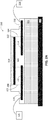
- FIG. 1A is a cross-sectional view of an integrated isolator device having a back-to-back configuration.
- Integrated isolator device 100 includes two isolators, 102 and 104, connected in series positioned over the same substrate 106.
- Each of isolators 102 and 104 has a pair of isolator components (e.g., coils or windings, capacitive plates).
- the isolator components are electromagnetically coupled, which may arise from the relative proximity of the isolator components to each other.
- Isolator 102 includes isolator component 108 and isolator component 110, which are positioned to electromagnetically couple with each other.
- Isolator 104 includes isolator component 112 and isolator component 114, which are positioned to electromagnetically couple with each other. As shown in FIG.
- both isolator components 110 and 112 are positioned over substrate 106, isolator component 108 is positioned over isolator component 110, and isolator component 112 is positioned over isolator component 114.
- isolators 102 and 104 are two capacitive coupling isolators where isolator components 108, 110, 112, 114 are capacitive plates.
- isolators 102 and 104 are two transformers where isolator components 108, 110, 112, 114 are coils.
- isolator components 108 and 110 are positioned in separate vertical layers of integrated isolator device 100 and to overlap, at least partially, with each other.
- isolator components 112 and 114 are positioned in separate vertical layers of integrated isolator device 100 and to overlap, at least partially, with each other.
- Isolator components 108 and 112 are positioned distal from substrate 106 and may be considered as "top" isolator components
- isolator components 110 and 114 are positioned proximate to substrate 106 and may be considered as "bottom” isolator components.
- bottom isolator components 110 and 114 are formed in the same plane of the integrated isolator device.
- top isolator components 108 and 112 are formed in the same plane of the integrated isolator device.
- isolators are connected in series by connecting the top isolator components to each other.
- isolators 102 and 104 are connected in series by coupling top isolator component 108 to top isolator component 112 through one or more conductors.
- wire bond 118 connects top isolator components 108 and 112 through contact 120 for top isolator component 108 and contact 122 for top isolator component 112.
- Top isolator components 108 and 112 may lack connections to external circuitry or ground potential, such that top isolator components 108 and 112 are considered to be floating.
- Bottom isolator components 110 and 114 are electrically isolated from one another, and in some embodiments, configured to operate at different voltages.
- bottom isolator component 110 may be configured to operate at a first voltage
- bottom isolator component 114 may be configured to operate at a second voltage different than the first voltage.
- Substrate 106 may include one or more dielectric materials (e.g., glass, polyimide). As shown in FIG. 1A , substrate 106 is positioned on paddle 124, which may be a portion of a lead frame for the packaged isolator. In some embodiments, substrate 106 may include a silicon die and an insulating layer formed over the silicon die, separating isolators 102 and 104 from the silicon die. According to the isolator configurations described herein, substrate 106 may be considered as a microfabricated die or microfabricated chip because both isolators 102 and 104 are formed on substrate 106.
- dielectric materials e.g., glass, polyimide
- microfabrication techniques may be implemented in fabricating the isolator by forming an array of the back-to-back isolators on a wafer, which is then subsequently diced to form individual die having both isolators 102 and 104. As part of packaging the isolator device, the die may then be positioned on paddle region 124 of a lead frame.
- Integrated isolator device 100 includes dielectric material 116 between isolators 102 and 104, as well as between top isolator component 108 and bottom isolator component 110, and between top isolator component 112 and bottom isolator component 114.
- FIG. 1A shows dielectric material 116 positioned between bottom isolator components 110, 114 and substrate 106, some embodiments may have bottom isolator components positioned in contact with substrate 106.
- Dielectric material 116 may be formed at least partially over top isolator components 108 and 112. In some embodiments, dielectric material 116 may be formed of multiple layers of one or more dielectric materials.
- Integrated isolator device 100 includes electrical contacts 130 and 132 coupled to bottom isolator components 110 and 114, respectively, which allow bottom isolator components 110 and 114 to connect to circuit(s) external to substrate 106. As shown in FIG. 1A , bottom isolator component 110 is connected to circuit 126 and bottom isolator component 114 is connected to circuit 128, such as by using bond wire(s). Circuits 126 and 128 may act as input and output circuitry for integrated isolator device 100.
- circuit 126 may include a transmitter and circuit 128 may include a receiver such that power and/or data is transferred from circuit 126 to circuit 128 through the back-to-back isolators by transferring from bottom isolator component 110 to top isolator component 108 in isolator 102 and then from top isolator component 112 to bottom isolator component 114 in isolator 104.
- integrated isolator device 100 may have a configuration allowing for transfer of signals and/or power in reverse through the isolator components.
- circuit 128 may include a transmitter and circuit 126 may include a receiver, and power and/or data is transferred from bottom isolator component 114 to top isolator component 112 in isolator 104 and then from top isolator component 108 to bottom isolator component 110 in isolator 102.
- integrated isolator device 100 may allow for bi-directional transfer of signals and/or power.
- Circuit 126 and circuit 128 may be configured to operate at different voltages or be referenced to different ground potentials, and integrated isolator device 100 may allow for circuits 126 and 128 to exchange data.
- Integrated isolator device 100 may be applied in a variety of applications ( e.g ., industrial, medical, consumer) where isolators may be used, including isolated control switches and isolated power supply controllers.
- a piece of industrial machinery may operate at a high voltage and be controlled by a computer of other control equipment that operates at a much lower voltage, with the two communicating via a back-to-back isolator of the type illustrated in FIG. 1A .
- Circuits 126 and 128 may electrically couple with two different power supplies and/or circuits 126 and 128 may have separate ground references. In this manner, the bottom isolator components of integrated isolator device 100 may operate in different voltage domains, where bottom isolator component 110 is configured to operate in one voltage domain and bottom isolator component 114 is configured to operate in a different voltage domain.
- integrated isolator device 100 may provide improved performance, particularly because of the reduced parasitic capacitance between one or both of top isolator components 108 and 112 and paddle portion 124.
- a capacitance between either or both top isolator components 108 and 112 and paddle portion 124 is less than a capacitance between a pair of isolator components in either or both isolators 102 and 104, such as between top isolator component 108 and bottom isolator component 110.
- This lower capacitance may be in part due to the thickness of substrate 106 and/or the relative lateral areas of top isolator components 108, 112 to their respective bottom isolator components 110, 114.
- one or more dielectric materials of substrate 106 may have a greater thickness than a region of dielectric material positioned between a pair of top and bottom isolator components, such as dielectric material 116 positioned between top isolator component 108 and bottom isolator component 110.
- substrate 106 is one or more dielectric materials (e.g ., glass)
- the thickness of substrate 106 may be in the range of 100 ⁇ m to 600 ⁇ m, or any value or range of values in that range.
- a thickness of dielectric material positioned between a top isolator component and its respective bottom isolator component may be in the range of 10 ⁇ m to 50 ⁇ m, or any value or range of values in that range.
- the top and bottom isolator components, and conductor(s) connected to the isolator components may have varying relative lateral areas to achieve desired performance, such as by reducing electric field interference and/or voltage imbalance during operation.
- electric field interference may occur from overlapping edges of conductive layers within the isolator device.
- Such electric field interference may be reduced or eliminated by having different lateral areas for top and bottom isolator components in an isolator because doing so reduces the amount of vertical overlapping edges for the top and bottom isolator components.
- some embodiments may include a top isolator component with a smaller lateral area than its respective bottom isolator component within an isolator.
- the top isolator component may be positioned to be, at least partially, within a periphery of the underlying bottom isolator component.
- a top isolator component may have a lateral area that is in the range of 75%-95% of its respective bottom isolator component.
- the isolator device may have a bottom isolator component with a smaller lateral area than its respective top isolator component.
- the bottom isolator component may be positioned to be, at least partially, within a periphery of the overlying top isolator component.
- a bottom isolator component may have a lateral area that is in the range of 75%-95% of its respective top isolator component.
- conductive regions integrated as part of the isolator device may be suitably sized and shaped to reduce electric field interference during operation.
- a conductive region connecting an electrical contact to a bottom isolator component may overlap with the respective top isolator component, and the conductive region may have one or more suitable dimensions to reduce electric field interference between the conductive region and the top isolator component.
- FIG. 1B is a top view of integrated isolator device 100 shown in FIG. 1A .
- Top views of top isolator components 108, 112 are shown by dotted outlines in FIG. 1B .
- Bottom isolator components 110, 114 and conductive regions 134, 136 connecting bottom isolator components 110, 114 to electrical contacts 130, 132, respectively, are shown by dashed outlines in FIG. 1B .
- conductive region 134 connects electrical contact 130 to bottom isolator component 110
- conductive region 136 connects electrical contact 132 to bottom isolator component 114.
- Conductive region 134 and bottom isolator component 110 may be formed in the same layer of integrated isolator device 100, and in some embodiments, of the same conductive material(s).
- Conductive region 136 and bottom isolator component 114 may be formed in the same layer of integrated isolator device 100, and in some embodiments, of the same conductive material(s).
- top isolator components 108, 112 may have smaller lateral areas than their respective bottom isolator components 110, 114.
- top isolator components 108, 112 may have one or more lateral dimensions, such as dimension D T of top isolator component 108, which is smaller than one or more lateral dimensions of bottom isolator components 110, 114, such as dimension D B of bottom isolator component 110.
- D B may be approximately 300 ⁇ m and D T may be approximately 260 ⁇ m.
- a periphery of a top isolator component may be at least partially within a periphery of its respective bottom isolator component in one or both of the isolators in the back-to-back isolator.
- the periphery of top isolator 112 shown by the dotted lines is within the periphery of bottom isolator component 114, shown by the dashed lines.
- Conductive regions 134, 136 may have a lateral dimension, such as dimension D C of conductive region 134. The lateral dimension of conductive regions 134, 136 may be smaller than a lateral dimension of bottom isolator components 110, 114.
- voltage imbalance during operation of a back-to-back isolator may occur between the two isolators connected in series where the two isolators in series do not experience a substantially similar amount of voltage even if the isolators have similar configurations. Voltage imbalance across the two isolators may negatively impact the performance of the back-to-back isolator.
- the two isolators may have varying lateral areas such that the isolator components of one isolator have different lateral areas in comparison to its corresponding isolator component in the other isolator. In some embodiments, an area of overlap between a top isolator component and its respective bottom isolator component may be different for the two isolators.
- top isolator component 108 may have a larger lateral area (e.g., dimension D T ) than top isolator component 112
- bottom isolator component 110 may have a larger lateral area ( e.g., dimension D B ) than bottom isolator component 114.
- one or both isolator components of one isolator may have a dimension relative to one or both isolator components of the other isolator in the range of 70% to 99%, or any value or range of values in that range.
- the relative lateral areas may accommodate any voltage imbalance between isolators 102 and 104 that would otherwise occur during operation.
- FIG. 2A is a cross-sectional view of an integrated isolator device having a back-to-back configuration.
- Integrated isolator device 200 includes isolator 102 having isolator components 110, 208 positioned to electromagnetically couple with one another, and isolator 104 having isolator components 114, 212 positioned to electromagnetically couple with one another. Similar to the integrated isolator device shown in FIG. 1A , top isolator components 208, 212 and bottom isolator components 110, 114 are positioned in separate vertical layers of integrated isolator device 200. In some embodiments, top isolator components 208 and 212 are formed in the same plane of the integrated isolator device.
- integrated isolator device 200 has an integrated conductor connecting top isolator components.
- conductive region 210 connects top isolator components 208 and 212 to each other.
- conductive region 210 and top isolator components 208, 212 may be formed of the same conductive material(s) and/or in the same layer of the integrated isolator device.
- conductive region 210 and top isolator components 208, 212 may be considered as a single isolator component that has one conductive region positioned to electromagnetically couple with bottom isolator component 110, another conductive region positioned to electromagnetically couple with bottom isolator component 114, and a third conductive region connecting the two conductive regions.
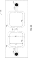
- FIG. 2B is an exemplary top view of integrated isolator device 200 shown in FIG. 2A .
- Bottom isolator components 110, 112 and conductive regions 134, 136 connecting bottom isolator components 110, 112 to electrical contacts 130, 132, respectively, are shown by dashed outlines in FIG. 2B .
- Top views of top isolator components 208, 212 and conductive region 210 connecting isolator components 208 and 212 are shown by dotted outlines in FIG. 2B .
- top isolator components 208, 212 may have greater lateral areas than their respective bottom isolator components 110, 114.
- top isolator components 208, 212 may have one or more lateral dimensions, such as dimension D T of top isolator component 208, which is greater than one or more lateral dimensions of bottom isolator components, 110, 114, such as dimension D B of bottom isolator component 110.
- a periphery of a bottom isolator component may be at least partially within a periphery of its respective top isolator component in one or both of the isolators in the back-to-back isolator.
- Conductive region 210 may have a lateral dimension, such as dimension D R of conductive region 210, that is smaller than a lateral dimension of top isolator components 208, 212, such as dimension D T of top isolator component 208. Reducing the area of conductive region 210 may reduce the effects of parasitic capacitance between conductive region 210 and an underlying conductor, such as paddle 124.
- Dimension D T of top isolator component 208 relative to dimension D B of bottom isolator component 110 may be in the range of 75%-95%, or any value or range of values in that range.
- Dimension D R of conductive region 210 relative to dimension D T of top isolator component 208 may be in the range of 1%-20%, or any value or range of values in that range. In some embodiments, dimension D R of conductive region 210 may be approximately 5% of dimension D T .
- FIG. 2C is an exemplary top view of integrated isolator device 200 shown in FIG. 2A having top isolator components with smaller lateral areas in comparison to their respective bottom isolator components.
- bottom isolator components 110, 112 and conductive regions 134, 136 connecting bottom isolator components 110, 112 to electrical contacts 130, 132, respectively are shown by dashed outlines in FIG. 2C .
- Top views of top isolator components 208, 212 and conductive region 210 connecting isolator components 208 and 212 are shown by dotted outlines in FIG. 2C .
- top isolator components 208, 212 may have smaller lateral areas than their respective bottom isolator components 110, 114.
- top isolator components 208, 212 may have one or more lateral dimensions, such as dimension D T of top isolator component 208, which is smaller than one or more lateral dimensions of bottom isolator components, 110, 114, such as dimension D B of bottom isolator component 110.
- a periphery of a top isolator component may be at least partially within a periphery of its respective bottom isolator component in one or both of the isolators in the back-to-back isolator.
- Conductive region 210 may have a lateral dimension, such as dimension D R of conductive region 210, that is smaller than a lateral dimension of top isolator components 208, 212, such as dimension D T of top isolator component 208. Reducing the area of conductive region 210 may reduce the effects of parasitic capacitance between conductive region 210 and an underlying conductor, such as paddle 124.
- the isolators connected in series are transformers where the top coils or windings are connected together.
- FIG. 3 is a top view of a back-to-back isolator having two transformers connected in series.
- Integrated isolator device 300 may have a similar structure as integrated isolator device 100, except that the isolators are transformers and the isolator components are coils or windings.
- One transformer includes top coil 308 and bottom coil 310.
- the other transformer includes top coil 312 and bottom coil 314.
- top coils 308 and 312 may be positioned within the periphery of bottom coils 310 and 314, respectively.
- Connecting top coils 308 and 312 in series may involve connecting the inner terminal of top coil 308 to the inner terminal of top coil 312 and connecting the outer terminal of top coil 308 to the outer terminal of top coil 312.
- some embodiments involve using wire bonds to connect the terminals of the top coils.
- wire bond 318a connects the inner terminal of top coil 308 to the inner terminal of top coil 312
- wire bond 318b connects the outer terminal of top coil 308 to the outer terminal of top coil 312.
- the bottom coils 310 and 314 connect with circuits, such as input and output circuits. Conductive traces connecting from the terminals of bottom coils 310 and 314 to electrical contacts may facilitate connecting bottom coils 310 and 314 to circuits. As shown in FIG.
- conductive trace 334a connects the inner terminal of bottom coil 310 to electrical contact 330a
- conductive trace 334b connects the outer terminal of bottom coil 310 to electrical contact 330b
- conductive trace 336a connects the inner terminal of bottom coil 314 to electrical contact 332a
- conductive trace 336b connects the outer terminal of bottom coil 314 to electrical contact 332b.
- Electrical contacts 330a, 330b may connect to one circuit (e.g ., transmitter, receiver), and electrical contacts 332a, 332b may connect to another circuit.
- One or more conductive traces may be positioned in a layer ( e.g ., metal layer) of the isolator vertically separated from one or more of the coils.
- conductive trace 336a may be positioned in a layer of isolator 300 vertically separated from both top coil 312 and bottom coil 314.
- conductive trace 336a may be positioned in a layer of isolator 300 below bottom coil 314 such that bottom coil 314 is in a layer between the layer having conductive trace 336a and a layer having top coil 312.
- Such a configuration may allow for conductive trace 336a to form an electrical connection between electrical contact 332a and the inner terminal of bottom coil 314 without conductive trace 336a intersecting the windings of bottom coil 314.
- conductive trace 334a may be positioned in a layer of isolator 300 below bottom coil 310, in some embodiments.
- some embodiments may have one or more conductive traces positioned in the same layer of the isolator as one or more coils.
- conductive trace 336b may be positioned in the same layer as bottom coil 314.
- Such a configuration may be suitable because conductive trace 336a may not intersect any windings of bottom coil 314 to form an electrical connection between the outer terminal of bottom coil 314 and electrical contact 332b.
- conductive trace 334b may be positioned in the same layer as bottom coil 310.
- connecting the top coils of back-to-back transformers may involve connecting an inner terminal of a first top coil to the outer terminal of a second top coil and connecting the outer terminal of the second top coil to the inner terminal of the first top coil.
- Such a configuration may provide a desired amount of signal balance during operation.
- Some embodiments relate to multi-channel integrated isolator devices where individual channels have a back-to-back configuration by connecting two isolators in series according to the techniques described herein.
- the multiple channels may be connected to different external circuitry and used to perform different operations, for example by using one channel to transfer one signal to one circuit and using another channel to transfer a different signal to a separate circuit.
- the multiple channels may be positioned on the same single substrate.
- both the substrate on which the back-to-back isolators are formed and circuit(s) acting as either an input or an output to the isolators are positioned on the same lead frame. In this manner, the back-to-back isolator configurations described herein may allow for less overall packaging footprint (packaging lateral space) because a separate lead frame may not be necessary for both input and output circuits.
- FIG. 4 shows a planar view of an exemplary multi-channel isolator device. Although FIG. 4 shows four channels, it should be appreciated that any suitable number of channels may be formed.
- each of the channels includes an isolator having a back-to-back configuration of integrated isolator device 100 shown in FIGs. 1A and 1B .
- One channel includes the integrated isolator device having top isolator components 108a, 112a, bottom isolator components 110a, 114a, which are connected to electrical contacts 130a, 132a, respectively.
- a second channel includes the integrated isolator device having top isolator components 108b, 112b, bottom isolator components 110b, 114b, which are connected to electrical contacts 130b, 132b, respectively.
- a third channel includes the integrated isolator device having top isolator components 108c, 112c, bottom isolator components 110c, 114c, which are connected to electrical contacts 130c, 132c, respectively.
- a fourth channel includes the integrated isolator device having top isolator components 108d, 112d, bottom isolator components 110d, 114d, which are connected to electrical contacts 130d, 132d, respectively.
- Substrate 116 on which all four back-to-back isolators are formed, is positioned on lead frame 404.
- substrate 116 may be positioned on a paddle portion 410 of lead frame 404.
- One set of bottom isolator components, including bottom isolator components 114a, 114b, 114c, 114d is connected to circuit(s) 128, and the other set of bottom isolator components, including bottom isolator components 110a, 110b, 110c, 110d is connected to circuit(s) 126.
- circuit(s) 126 is positioned on lead frame 402, which is separate from lead frame 404. Both substrate 116 and circuit(s) 128 are positioned on lead frame 404.
- Lead frames 402 and 404 have lead frame fingers for making external connections. Specifically, lead frame 402 has fingers 406a, 406b, 406c, 406d, which may each connect one of the respective four channels to external circuitry. Lead frame 404 has fingers 408a, 408b, 408c, 408d, which may each connect one of the respective four channels to external circuitry.
- isolator components e.g., coils, plates
- dielectric materials examples include silicon dioxide and polyimide.
- the substrate of the integrated device may be a silicon substrate and may include an insulating material (e.g ., polyimide) over the silicon substrate.
- a non-limiting example of a dielectric material that may be used for dielectric material 116 of the integrated isolator device described herein is polyimide.
- the back-to-back integrated isolator devices described herein may be used in various applications. For example, consumer electronics, energy, healthcare, industrial, automotive, medical, aerospace, security, communications, and instrumentation applications may all make use of the technology described here. For example, data transfer and/or power transfer between galvanically isolated systems may be accomplished with the integrated isolator devices described herein.
- medical equipment in a room in which a medical procedure is being performed may be galvanically isolated from a control system in a control room.
- a piece of medical imaging equipment and/or monitors in the room in which the procedure is being performed may be isolated from a system controlling operation of the imaging equipment and/or display.
- the isolator may be a back-to-back integrated isolator device of any of the types described herein, and the isolated signal path may be analog or digital.
- industrial equipment may be isolated from a control system controlling the equipment.
- high wattage motors may be isolated from control systems controlling their operation by an integrated isolator device of the types described herein.
- the control systems may operate at a lower wattage than the high wattage motors used by the industrial equipment.
- the isolator may be disposed on a circuit board on which various circuit components connected to the motors and/or control equipment are included.
- FIG. 5 is a schematic diagram showing an exemplary application of using an integrated isolator device of the types described herein for providing power isolation between an industrial apparatus and a computing device.
- system 500 includes integrated isolator device 502, which may isolate a comparatively high voltage device from a comparatively low voltage device.
- integrated isolator device 502 connects industrial motor 504 to computing device 506 via cable 508.
- the computing device 506 may be a personal computer (PC), a server, or another computing device.
- isolator 502 is depicted as being integrated as part of industrial motor 504, isolator 502 may be in practice arranged as a separate component connected to both industrial motor 504 and computing device 506. Other such devices may also make use of the integrated isolator devices described herein.
- integrated isolator device 502 may be used for voltage isolation between a turbine and computing device 506.
- some aspects may be embodied as one or more methods.
- the acts performed as part of the method may be ordered in any suitable way. Accordingly, embodiments may be constructed in which acts are performed in an order different than illustrated, which may include performing some acts simultaneously, even though shown as sequential acts in illustrative embodiments.
- the terms “approximately” and “about” may be used to mean within ⁇ 20% of a target value in some embodiments, within ⁇ 10% of a target value in some embodiments, within ⁇ 5% of a target value in some embodiments, and yet within ⁇ 2% of a target value in some embodiments.
- the terms “approximately” and “about” may include the target value.
Landscapes
- Engineering & Computer Science (AREA)
- Physics & Mathematics (AREA)
- Electromagnetism (AREA)
- Microelectronics & Electronic Packaging (AREA)
- Semiconductor Integrated Circuits (AREA)
- Power Engineering (AREA)
- Auxiliary Devices For And Details Of Packaging Control (AREA)
Abstract
Description
- The present application relates to galvanic isolators providing galvanic isolation between circuits.
- Isolators provide electrical isolation between circuits which communicate with each other. In some situations, circuits which communicate with each other operate at different voltages, for instance one at a relatively high voltage and the other at a relatively low voltage. In some situations, the circuits are referenced to different electrical ground potentials. Isolators can be used to electrically isolate circuits in either of these situations. Connecting multiple isolators in series may increase the amount of isolation between the circuits.
- Isolators having a back-to-back configuration for providing electrical isolation between two circuits are described, in which multiple isolators formed on a single, monolithic substrate are connected in series to achieve a higher amount of electrical isolation for a single substrate than for a single isolator formed on substrate. Connecting the top isolator components, which are distal from the single substrate, may provide electrical isolation to the top isolator components. The back-to-back isolator may provide one or more communication channels for transfer of information and/or power between the circuits connected to the bottom isolator components.
- In some embodiments, an integrated isolator device is provided. The integrated isolator device comprises a substrate, and a first isolator component and a second isolator component positioned over the substrate. The integrated isolator device further comprises a third isolator component positioned over the first isolator component and a fourth isolator component positioned over the second isolator component. The integrated isolator device further comprises at least one conductor connecting the third isolator component to the fourth isolator component.
- In some embodiments, an integrated isolator device is provided. The integrated isolator device comprises a substrate, and a first isolator component and a second isolator component positioned over the substrate. The integrated isolator device further comprises at least one third isolator component configured to electromagnetically couple with the first isolator component and the second isolator component. The first isolator component and the second isolator component are positioned between the at least one third isolator component and the substrate. The integrated isolator device further comprises a first electrical contact coupled to the first isolator component and a second electrical contact coupled to the second isolator component.
- In some embodiments, a system comprising an isolator, at least one first circuit, and at least one second circuit is provided. The isolator comprises a substrate, and a first isolator component and a second isolator component positioned over the substrate. The isolator further comprises at least one third isolator component positioned over the first isolator component and the second isolator component. The at least one first circuit is coupled to the first isolator component and configured to operate in a first voltage domain. The at least one second circuit coupled to the second isolator component and configured to operate in a second voltage domain different than the first voltage domain.
- Various aspects and embodiments of the application will be described with reference to the following figures. It should be appreciated that the figures are not necessarily drawn to scale. Items appearing in multiple figures are indicated by the same reference number in all the figures in which they appear.
-
FIG. 1A is a cross-sectional view of an integrated isolator device having a back-to-back configuration. -
FIG. 1B is a top view of the integrated isolator device shown inFIG. 1A . -
FIG. 2A is a cross-sectional view of an integrated isolator device having a back-to-back configuration. -
FIG. 2B is an exemplary top view of the integrated isolator device shown inFIG. 2A . -
FIG. 2C is an exemplary top view of the integrated isolator device shown inFIG. 2A . -
FIG. 3 is a top view of an integrated isolator device having two transformers connected in series. -
FIG. 4 is a top view of an integrated isolator device positioned on a lead frame and connected to two circuits. -
FIG. 5 is a schematic diagram showing an exemplary application of using an integrated isolator device of the types described herein for providing power isolation between an industrial apparatus and a computing device. - Aspects of the present application relate to a back-to-back isolator formed on a single monolithic integrated device. The back-to-back isolator includes two or more isolators connected in series formed on a single substrate (e.g., glass substrate, ceramic substrate, semiconductor substrate). One approach for achieving a back-to-back configuration is to connect two isolators on separate substrates in series to achieve an effective isolation equaling the cumulative isolation properties of the two isolators. In contrast, aspects of the present application provide back-to-back isolators formed on a single substrate. A benefit of a monolithic configuration is that the total isolation may be the cumulative isolation properties of two isolators, with less overall footprint (substrate area) because the structure has substantially similar area as a single isolator (e.g., approximately 10%-15% larger than a single isolator). For example, if each isolator in the back-to-back configuration can withstand 600 V, then the cumulative isolation the back-to-back isolator can handle is approximately 1200 V. Additionally, forming the back-to-back isolator on a single substrate reduces costs in comparison to a multi-substrate back-to-back configuration because less substrate area is used. The higher isolation provided by the back-to-back isolator on a single substrate can be implemented in high voltage applications, such as industrial (e.g., machine monitoring) and healthcare or medical applications, which typically require high isolation voltages-for example, the ability to protect against surge events (e.g., 15kV - 20kV)-that can be challenging to achieve with single isolators. More generally, it may be desirable to isolate voltages from approximately 400V up to approximately 20kV, whether in steady state operation or as surge events.
- In particular, aspects of the present application relate to a back-to-back isolator structure that includes a first pair of isolator components (e.g., coils or windings, or capacitive plates) forming one of the isolators and a second pair of isolator components forming the other isolator. The isolator components in each pair are arranged vertically within the integrated device, forming a top isolator component and a bottom isolator component at different vertical levels separated by dielectric material. The top isolator components are electrically shorted together and are electrically isolated from the underlying substrate and the bottom isolator components, forming floating top isolator components in the integrated device. The bottom isolator components are configured to act as inputs and outputs for the back-to-back isolator. For example, a bottom isolator component of the first pair may electrically connect to a transmitter while a bottom isolator component of the second pair may electrically connect to a receiver.
- To achieve a desired performance in a back-to-back isolator, including a desired voltage capability, the capacitance between the isolator components of a pair (e.g., the top isolator component and bottom isolator component) is high to allow for electric field coupling or magnetic field coupling. However, parasitic capacitance may exist between the floating isolator components and an underlying conductor. For example, in some embodiments, the isolator may be disposed on a paddle portion of a lead frame as part of packaging for the isolator. A parasitic capacitance may exist between the floating isolator components and the paddle portion. The parasitic capacitance between the floating isolator components and an underlying conductor may reduce the voltage capabilities that the isolator may otherwise be configured to achieve. For example, the parasitic capacitance may result in a voltage imbalance between the two isolators in the back-to-back configuration and, during operation, the resulting isolator may be limited by the device connected to the isolator having the higher portion of the voltage.
- The back-to-back configuration described in the present application, having floating top isolator components, may provide the benefit of reducing or eliminating parasitic capacitance between the top isolator components and an underlying conductor, such as the underlying substrate (e.g., silicon substrate) and/or a paddle portion of the lead frame that the isolator is positioned on as part of packaging for the isolator. In contrast to floating the bottom isolator components, floating the top isolator components increases the thickness of the dielectric material between the floating isolator components and the underlying conductor, which may reduce or eliminate the parasitic capacitance. The back-to-back isolator may be formed on a microfabricated substrate (e.g., glass substrate, silicon substrate) having a substantial thickness of dielectric material (e.g., >400 µm for glass) such that when the isolator is packaged by positioning the substrate on a lead frame, the resulting packaged isolator has a substantially low parasitic capacitance between the top isolator components and the underlying paddle portion of the lead frame to reduce the impact of the parasitic capacitance on the performance capabilities of the isolator. In some embodiments, the back-to-back isolator may be formed, using suitable microfabrication techniques, on a dielectric substrate (e.g., glass substrate), and the dielectric substrate may contact the paddle portion of the lead frame in the packaged isolator. In some embodiments, the back-to-back isolator may be formed on an insulating layer (e.g., polyimide layer), which is over a silicon substrate (e.g., silicon die or chip), and the silicon substrate may contact the paddle portion in the packaged isolator. In such embodiments, the thickness of the insulating layer may act to reduce the parasitic capacitance between the top isolator components and the silicon substrate, which may have a conductive contact with the underlying paddle portion.
- In addition, the lateral area of the top isolator components relative to their respective bottom isolator components may further impact performance of the back-to-back isolator. In some embodiments, the isolator may have top isolator components that have a smaller lateral area in comparison to their respective bottom isolator components. For example, a top isolator component may have a lateral area that is in the range of 75%-95% of their respective bottom isolator component. Such a configuration may further reduce or eliminate any parasitic capacitance between the top isolator components and an underlying conductor in the resulting packaged isolator because the bottom isolator components may act to shield the top isolator components from the underlying conductor. In some embodiments, the top isolator components may be connected in a manner that reduces or eliminates parasitic capacitance, such as by connecting the top isolator components with an external bond wire or with a conductor integrated in the isolator. The integrated conductor connecting the top isolator components may have one or more dimensions smaller than a lateral dimension of one or both of the top isolator components. For example, the integrated conductor may have a width of approximately 5% the width of one or both of the top isolator components. In some embodiments, the integrated conductor may be formed in the same layer of the top isolator components as a conductive region connecting the top isolator components. In some embodiments, the integrated conductor may be formed of a wire bond integrated in the isolator as one or more metal layers formed over the top isolator components.
- Some aspects of the present application relate to structural features that may allow for further desired performance of the back-to-back isolator by reducing or eliminating electric field interference in regions where there is vertical overlap between a connection to a top or bottom isolator component and the other isolator component in the pair. For example, a conductor connecting a contact pad to a bottom isolator component may vertically overlap with its respective top isolator component, and the region of overlap may reduce performance of the isolator because of electrical interference occurring at this region. The impact of such electric field interference regions may be reduced or eliminated by reducing the amount of vertical overlap between conductor(s) connecting to the top and bottom isolator components and their respective isolator component in the isolator pair. For example, connecting the top isolator components using an external bond wire and having a smaller lateral area for the top isolator components in comparison to the bottom isolator components may substantially reduce or completely eliminate electric field interference regions that may otherwise contribute to reduced performance.
- The back-to-back isolator configurations described herein may be applied to various types of isolator technology, including inductive coupling isolators and capacitive coupling isolators, by forming different types of isolator components on the substrate. In embodiments where the isolator components are coils or windings, the back-to-back isolator includes two transformers connected in series. In embodiments where the isolator components are capacitive plates, the back-to-back isolator includes two capacitive isolators connected in series. Some embodiments may provide increased working voltage, withstand or isolation rating, and surge robustness performance compared to alternative constructions. The back-to-back configuration may facilitate simplicity of design and deliver cost savings over separate die construction. The back-to-back isolator of the present application floats the top isolator components, while the bottom isolator components are connected to circuitry coupled to respective isolated potentials. With this approach, both pairs of isolator components can coexist on a single substrate where the top isolator components are maintained in a floating state. In embodiments where the substrate is a semiconductor substrate, the top isolator components may connect to a floating paddle within the package. In embodiments where the substrate is a glass substrate, a floating paddle may not be necessary to achieve a floating state for the top isolator components. , such as by connecting to a floating paddle within the package.
- The aspects and embodiments described above, as well as additional aspects and embodiments, are described further below. These aspects and/or embodiments may be used individually, all together, or in any combination of two or more, as the application is not limited in this respect.
- Aspects of the present application relate to structures of a single monolithic back-to-back isolator that facilitates a desired isolation performance, including by reducing or eliminating parasitic capacitance between the isolators on the device with an underlying conductor, such as a paddle portion of a lead frame in the packaged version of the device. According to some embodiments, reduced parasitic capacitance can be achieved by connecting the top isolator components such that the two isolators are connected in series and have a back-to-back configuration, and using the bottom isolator components as inputs and outputs.
FIG. 1A is a cross-sectional view of an integrated isolator device having a back-to-back configuration.Integrated isolator device 100 includes two isolators, 102 and 104, connected in series positioned over thesame substrate 106. Each ofisolators Isolator 102 includesisolator component 108 andisolator component 110, which are positioned to electromagnetically couple with each other.Isolator 104 includesisolator component 112 andisolator component 114, which are positioned to electromagnetically couple with each other. As shown inFIG. 1A , bothisolator components substrate 106,isolator component 108 is positioned overisolator component 110, andisolator component 112 is positioned overisolator component 114. In some embodiments,isolators isolator components isolators isolator components - As shown in
FIG. 1A ,isolator components integrated isolator device 100 and to overlap, at least partially, with each other. Similarly,isolator components integrated isolator device 100 and to overlap, at least partially, with each other.Isolator components substrate 106 and may be considered as "top" isolator components, whileisolator components substrate 106 and may be considered as "bottom" isolator components. In some embodiments,bottom isolator components top isolator components - According to some aspects of the back-to-back configurations described herein, isolators are connected in series by connecting the top isolator components to each other. As shown in
FIG. 1A ,isolators top isolator component 108 totop isolator component 112 through one or more conductors. In particular,wire bond 118 connectstop isolator components contact 120 fortop isolator component 108 and contact 122 fortop isolator component 112.Top isolator components top isolator components Bottom isolator components bottom isolator component 110 may be configured to operate at a first voltage, andbottom isolator component 114 may be configured to operate at a second voltage different than the first voltage. -
Substrate 106 may include one or more dielectric materials (e.g., glass, polyimide). As shown inFIG. 1A ,substrate 106 is positioned onpaddle 124, which may be a portion of a lead frame for the packaged isolator. In some embodiments,substrate 106 may include a silicon die and an insulating layer formed over the silicon die, separatingisolators substrate 106 may be considered as a microfabricated die or microfabricated chip because bothisolators substrate 106. For example, microfabrication techniques may be implemented in fabricating the isolator by forming an array of the back-to-back isolators on a wafer, which is then subsequently diced to form individual die having bothisolators paddle region 124 of a lead frame. -
Integrated isolator device 100 includesdielectric material 116 betweenisolators top isolator component 108 andbottom isolator component 110, and betweentop isolator component 112 andbottom isolator component 114. AlthoughFIG. 1A showsdielectric material 116 positioned betweenbottom isolator components substrate 106, some embodiments may have bottom isolator components positioned in contact withsubstrate 106.Dielectric material 116 may be formed at least partially overtop isolator components dielectric material 116 may be formed of multiple layers of one or more dielectric materials. -
Integrated isolator device 100 includeselectrical contacts bottom isolator components bottom isolator components substrate 106. As shown inFIG. 1A ,bottom isolator component 110 is connected tocircuit 126 andbottom isolator component 114 is connected tocircuit 128, such as by using bond wire(s).Circuits integrated isolator device 100. In some embodiments,circuit 126 may include a transmitter andcircuit 128 may include a receiver such that power and/or data is transferred fromcircuit 126 tocircuit 128 through the back-to-back isolators by transferring frombottom isolator component 110 totop isolator component 108 inisolator 102 and then fromtop isolator component 112 tobottom isolator component 114 inisolator 104. In some embodiments,integrated isolator device 100 may have a configuration allowing for transfer of signals and/or power in reverse through the isolator components. In such embodiments,circuit 128 may include a transmitter andcircuit 126 may include a receiver, and power and/or data is transferred frombottom isolator component 114 totop isolator component 112 inisolator 104 and then fromtop isolator component 108 tobottom isolator component 110 inisolator 102. In this manner,integrated isolator device 100 may allow for bi-directional transfer of signals and/or power. -
Circuit 126 andcircuit 128 may be configured to operate at different voltages or be referenced to different ground potentials, andintegrated isolator device 100 may allow forcircuits Integrated isolator device 100 may be applied in a variety of applications (e.g., industrial, medical, consumer) where isolators may be used, including isolated control switches and isolated power supply controllers. As an example, a piece of industrial machinery may operate at a high voltage and be controlled by a computer of other control equipment that operates at a much lower voltage, with the two communicating via a back-to-back isolator of the type illustrated inFIG. 1A .Circuits circuits integrated isolator device 100 may operate in different voltage domains, wherebottom isolator component 110 is configured to operate in one voltage domain andbottom isolator component 114 is configured to operate in a different voltage domain. - According to aspects of the present application,
integrated isolator device 100 may provide improved performance, particularly because of the reduced parasitic capacitance between one or both oftop isolator components paddle portion 124. In particular, a capacitance between either or bothtop isolator components paddle portion 124 is less than a capacitance between a pair of isolator components in either or bothisolators top isolator component 108 andbottom isolator component 110. This lower capacitance may be in part due to the thickness ofsubstrate 106 and/or the relative lateral areas oftop isolator components bottom isolator components substrate 106 may have a greater thickness than a region of dielectric material positioned between a pair of top and bottom isolator components, such asdielectric material 116 positioned betweentop isolator component 108 andbottom isolator component 110. In embodiments wheresubstrate 106 is one or more dielectric materials (e.g., glass), the thickness ofsubstrate 106 may be in the range of 100 µm to 600 µm, or any value or range of values in that range. In contrast, a thickness of dielectric material positioned between a top isolator component and its respective bottom isolator component may be in the range of 10 µm to 50 µm, or any value or range of values in that range. - According to aspects of the present application, the top and bottom isolator components, and conductor(s) connected to the isolator components may have varying relative lateral areas to achieve desired performance, such as by reducing electric field interference and/or voltage imbalance during operation. In particular, electric field interference may occur from overlapping edges of conductive layers within the isolator device. Such electric field interference may be reduced or eliminated by having different lateral areas for top and bottom isolator components in an isolator because doing so reduces the amount of vertical overlapping edges for the top and bottom isolator components. Accordingly, some embodiments may include a top isolator component with a smaller lateral area than its respective bottom isolator component within an isolator. The top isolator component may be positioned to be, at least partially, within a periphery of the underlying bottom isolator component. For example, a top isolator component may have a lateral area that is in the range of 75%-95% of its respective bottom isolator component. In some embodiments, the isolator device may have a bottom isolator component with a smaller lateral area than its respective top isolator component. Similarly, the bottom isolator component may be positioned to be, at least partially, within a periphery of the overlying top isolator component. For example, a bottom isolator component may have a lateral area that is in the range of 75%-95% of its respective top isolator component. In addition, conductive regions integrated as part of the isolator device may be suitably sized and shaped to reduce electric field interference during operation. In some embodiments, a conductive region connecting an electrical contact to a bottom isolator component may overlap with the respective top isolator component, and the conductive region may have one or more suitable dimensions to reduce electric field interference between the conductive region and the top isolator component. Although the above discussion is in the context of an isolator having different lateral areas for its top isolator component and its bottom isolator component, it should be appreciate that some embodiments may involve having one or both isolators in the back-to-back configuration where the top and bottom isolator components have substantially the same lateral area.
-
FIG. 1B is a top view ofintegrated isolator device 100 shown inFIG. 1A . Top views oftop isolator components FIG. 1B .Bottom isolator components conductive regions bottom isolator components electrical contacts FIG. 1B . In particular,conductive region 134 connectselectrical contact 130 tobottom isolator component 110, andconductive region 136 connectselectrical contact 132 tobottom isolator component 114.Conductive region 134 andbottom isolator component 110 may be formed in the same layer ofintegrated isolator device 100, and in some embodiments, of the same conductive material(s). Similarly,conductive region 136 andbottom isolator component 114 may be formed in the same layer ofintegrated isolator device 100, and in some embodiments, of the same conductive material(s). - As shown in
FIG. 1B ,top isolator components bottom isolator components top isolator components top isolator component 108, which is smaller than one or more lateral dimensions ofbottom isolator components bottom isolator component 110. As a non-limiting example, DB may be approximately 300 µm and DT may be approximately 260 µm. In some embodiments, a periphery of a top isolator component may be at least partially within a periphery of its respective bottom isolator component in one or both of the isolators in the back-to-back isolator. For example, the periphery oftop isolator 112, shown by the dotted lines, is within the periphery ofbottom isolator component 114, shown by the dashed lines.Conductive regions conductive region 134. The lateral dimension ofconductive regions bottom isolator components - In addition, voltage imbalance during operation of a back-to-back isolator may occur between the two isolators connected in series where the two isolators in series do not experience a substantially similar amount of voltage even if the isolators have similar configurations. Voltage imbalance across the two isolators may negatively impact the performance of the back-to-back isolator. To account for such voltage imbalance, the two isolators may have varying lateral areas such that the isolator components of one isolator have different lateral areas in comparison to its corresponding isolator component in the other isolator. In some embodiments, an area of overlap between a top isolator component and its respective bottom isolator component may be different for the two isolators. For example,
top isolator component 108 may have a larger lateral area (e.g., dimension DT ) thantop isolator component 112, andbottom isolator component 110 may have a larger lateral area (e.g., dimension DB ) thanbottom isolator component 114. In some embodiments, one or both isolator components of one isolator may have a dimension relative to one or both isolator components of the other isolator in the range of 70% to 99%, or any value or range of values in that range. In such instances, the relative lateral areas may accommodate any voltage imbalance betweenisolators -
FIG. 2A is a cross-sectional view of an integrated isolator device having a back-to-back configuration.Integrated isolator device 200 includesisolator 102 havingisolator components isolator 104 havingisolator components FIG. 1A ,top isolator components bottom isolator components integrated isolator device 200. In some embodiments,top isolator components - In contrast to
integrated isolator device 100 that haswire bond 118 connectingtop isolator components isolator device 200 has an integrated conductor connecting top isolator components. In particular, as shown inFIG. 2A ,conductive region 210 connectstop isolator components conductive region 210 andtop isolator components conductive region 210 andtop isolator components bottom isolator component 110, another conductive region positioned to electromagnetically couple withbottom isolator component 114, and a third conductive region connecting the two conductive regions. -
FIG. 2B is an exemplary top view ofintegrated isolator device 200 shown inFIG. 2A .Bottom isolator components conductive regions bottom isolator components electrical contacts FIG. 2B . Top views oftop isolator components conductive region 210 connectingisolator components FIG. 2B . - As shown in
FIG. 2B ,top isolator components bottom isolator components top isolator components top isolator component 208, which is greater than one or more lateral dimensions of bottom isolator components, 110, 114, such as dimension DB ofbottom isolator component 110. In some embodiments, a periphery of a bottom isolator component may be at least partially within a periphery of its respective top isolator component in one or both of the isolators in the back-to-back isolator. For example, the periphery ofbottom isolator 114, shown by the dashed lines, is within the periphery oftop isolator component 212, shown by the dotted lines.Conductive region 210 may have a lateral dimension, such as dimension DR ofconductive region 210, that is smaller than a lateral dimension oftop isolator components top isolator component 208. Reducing the area ofconductive region 210 may reduce the effects of parasitic capacitance betweenconductive region 210 and an underlying conductor, such aspaddle 124. Dimension DT oftop isolator component 208 relative to dimension DB ofbottom isolator component 110 may be in the range of 75%-95%, or any value or range of values in that range. Dimension DR ofconductive region 210 relative to dimension DT oftop isolator component 208 may be in the range of 1%-20%, or any value or range of values in that range. In some embodiments, dimension DR ofconductive region 210 may be approximately 5% of dimension DT . - In some embodiments of
integrated isolator device 200 shown inFIG. 2A , the top isolator components may have smaller lateral areas than their respective bottom isolator components.FIG. 2C is an exemplary top view ofintegrated isolator device 200 shown inFIG. 2A having top isolator components with smaller lateral areas in comparison to their respective bottom isolator components. As withFIG. 2B ,bottom isolator components conductive regions bottom isolator components electrical contacts FIG. 2C . Top views oftop isolator components conductive region 210 connectingisolator components FIG. 2C . - As shown in
FIG. 2C ,top isolator components bottom isolator components top isolator components top isolator component 208, which is smaller than one or more lateral dimensions of bottom isolator components, 110, 114, such as dimension DB ofbottom isolator component 110. In some embodiments, a periphery of a top isolator component may be at least partially within a periphery of its respective bottom isolator component in one or both of the isolators in the back-to-back isolator. For example, the periphery oftop isolator 212, shown by the dotted lines, is within the periphery ofbottom isolator component 114, shown by the dashed lines.Conductive region 210 may have a lateral dimension, such as dimension DR ofconductive region 210, that is smaller than a lateral dimension oftop isolator components top isolator component 208. Reducing the area ofconductive region 210 may reduce the effects of parasitic capacitance betweenconductive region 210 and an underlying conductor, such aspaddle 124. - In some embodiments, the isolators connected in series are transformers where the top coils or windings are connected together.
FIG. 3 is a top view of a back-to-back isolator having two transformers connected in series.Integrated isolator device 300 may have a similar structure asintegrated isolator device 100, except that the isolators are transformers and the isolator components are coils or windings. One transformer includestop coil 308 andbottom coil 310. The other transformer includestop coil 312 andbottom coil 314. As shown inFIG. 3 ,top coils bottom coils top coils top coil 308 to the inner terminal oftop coil 312 and connecting the outer terminal oftop coil 308 to the outer terminal oftop coil 312. As shown inFIG. 3 , some embodiments involve using wire bonds to connect the terminals of the top coils. In particular,wire bond 318a connects the inner terminal oftop coil 308 to the inner terminal oftop coil 312, andwire bond 318b connects the outer terminal oftop coil 308 to the outer terminal oftop coil 312. The bottom coils 310 and 314 connect with circuits, such as input and output circuits. Conductive traces connecting from the terminals ofbottom coils bottom coils FIG. 3 ,conductive trace 334a connects the inner terminal ofbottom coil 310 toelectrical contact 330a,conductive trace 334b connects the outer terminal ofbottom coil 310 toelectrical contact 330b,conductive trace 336a connects the inner terminal ofbottom coil 314 toelectrical contact 332a, andconductive trace 336b connects the outer terminal ofbottom coil 314 toelectrical contact 332b.Electrical contacts electrical contacts - One or more conductive traces may be positioned in a layer (e.g., metal layer) of the isolator vertically separated from one or more of the coils. As an example,
conductive trace 336a may be positioned in a layer ofisolator 300 vertically separated from bothtop coil 312 andbottom coil 314. In some embodiments,conductive trace 336a may be positioned in a layer ofisolator 300 belowbottom coil 314 such thatbottom coil 314 is in a layer between the layer havingconductive trace 336a and a layer havingtop coil 312. Such a configuration may allow forconductive trace 336a to form an electrical connection betweenelectrical contact 332a and the inner terminal ofbottom coil 314 withoutconductive trace 336a intersecting the windings ofbottom coil 314. Similarly,conductive trace 334a may be positioned in a layer ofisolator 300 belowbottom coil 310, in some embodiments. In contrast, some embodiments may have one or more conductive traces positioned in the same layer of the isolator as one or more coils. For example,conductive trace 336b may be positioned in the same layer asbottom coil 314. Such a configuration may be suitable becauseconductive trace 336a may not intersect any windings ofbottom coil 314 to form an electrical connection between the outer terminal ofbottom coil 314 andelectrical contact 332b. Similarly,conductive trace 334b may be positioned in the same layer asbottom coil 310. - In some embodiments, connecting the top coils of back-to-back transformers may involve connecting an inner terminal of a first top coil to the outer terminal of a second top coil and connecting the outer terminal of the second top coil to the inner terminal of the first top coil. Such a configuration may provide a desired amount of signal balance during operation.
- Some embodiments relate to multi-channel integrated isolator devices where individual channels have a back-to-back configuration by connecting two isolators in series according to the techniques described herein. The multiple channels may be connected to different external circuitry and used to perform different operations, for example by using one channel to transfer one signal to one circuit and using another channel to transfer a different signal to a separate circuit. According to aspects of the present application, the multiple channels may be positioned on the same single substrate. In packaging the multi-channel isolator, both the substrate on which the back-to-back isolators are formed and circuit(s) acting as either an input or an output to the isolators are positioned on the same lead frame. In this manner, the back-to-back isolator configurations described herein may allow for less overall packaging footprint (packaging lateral space) because a separate lead frame may not be necessary for both input and output circuits.
-
FIG. 4 shows a planar view of an exemplary multi-channel isolator device. AlthoughFIG. 4 shows four channels, it should be appreciated that any suitable number of channels may be formed. In the multi-channel isolator device shown inFIG. 4 , each of the channels includes an isolator having a back-to-back configuration ofintegrated isolator device 100 shown inFIGs. 1A and1B . One channel includes the integrated isolator device havingtop isolator components bottom isolator components electrical contacts top isolator components bottom isolator components electrical contacts top isolator components bottom isolator components electrical contacts top isolator components bottom isolator components electrical contacts Substrate 116, on which all four back-to-back isolators are formed, is positioned onlead frame 404. In particular,substrate 116 may be positioned on a paddle portion 410 oflead frame 404. One set of bottom isolator components, includingbottom isolator components bottom isolator components FIG. 4 , circuit(s) 126 is positioned onlead frame 402, which is separate fromlead frame 404. Bothsubstrate 116 and circuit(s) 128 are positioned onlead frame 404. Lead frames 402 and 404 have lead frame fingers for making external connections. Specifically,lead frame 402 hasfingers Lead frame 404 hasfingers - Examples of conductive materials that may be used to form isolator components (e.g., coils, plates) in embodiments of the integrated isolator device described herein, such as
isolator components conductive regions conductive traces - Examples of dielectric materials that may be used in a substrate of the integrated isolator device described herein, such as
substrate 106, include silicon dioxide and polyimide. In some embodiments, the substrate of the integrated device may be a silicon substrate and may include an insulating material (e.g., polyimide) over the silicon substrate. - A non-limiting example of a dielectric material that may be used for
dielectric material 116 of the integrated isolator device described herein is polyimide. - The back-to-back integrated isolator devices described herein may be used in various applications. For example, consumer electronics, energy, healthcare, industrial, automotive, medical, aerospace, security, communications, and instrumentation applications may all make use of the technology described here. For example, data transfer and/or power transfer between galvanically isolated systems may be accomplished with the integrated isolator devices described herein. As one example, medical equipment in a room in which a medical procedure is being performed may be galvanically isolated from a control system in a control room. For instance, a piece of medical imaging equipment and/or monitors in the room in which the procedure is being performed may be isolated from a system controlling operation of the imaging equipment and/or display. The isolator may be a back-to-back integrated isolator device of any of the types described herein, and the isolated signal path may be analog or digital.
- As another example, industrial equipment may be isolated from a control system controlling the equipment. For example, high wattage motors may be isolated from control systems controlling their operation by an integrated isolator device of the types described herein. The control systems may operate at a lower wattage than the high wattage motors used by the industrial equipment. The isolator may be disposed on a circuit board on which various circuit components connected to the motors and/or control equipment are included.
-
FIG. 5 is a schematic diagram showing an exemplary application of using an integrated isolator device of the types described herein for providing power isolation between an industrial apparatus and a computing device. In particular,system 500 includesintegrated isolator device 502, which may isolate a comparatively high voltage device from a comparatively low voltage device. In the example shown inFIG. 5 ,integrated isolator device 502 connectsindustrial motor 504 tocomputing device 506 viacable 508. Thecomputing device 506 may be a personal computer (PC), a server, or another computing device. Althoughisolator 502 is depicted as being integrated as part ofindustrial motor 504,isolator 502 may be in practice arranged as a separate component connected to bothindustrial motor 504 andcomputing device 506. Other such devices may also make use of the integrated isolator devices described herein. For example, instead ofindustrial motor 504, integratedisolator device 502 may be used for voltage isolation between a turbine andcomputing device 506. - Other uses of the integrated isolator devices described herein are also possible, as those examples described are non-limiting.
- Also, as described, some aspects may be embodied as one or more methods. The acts performed as part of the method may be ordered in any suitable way. Accordingly, embodiments may be constructed in which acts are performed in an order different than illustrated, which may include performing some acts simultaneously, even though shown as sequential acts in illustrative embodiments.
- The terms "approximately" and "about" may be used to mean within ±20% of a target value in some embodiments, within ±10% of a target value in some embodiments, within ±5% of a target value in some embodiments, and yet within ±2% of a target value in some embodiments. The terms "approximately" and "about" may include the target value.
Claims (15)
- An integrated isolator device comprising:a substrate;a first isolator component and a second isolator component positioned over the substrate;a third isolator component positioned over the first isolator component;a fourth isolator component positioned over the second isolator component; andat least one conductor connecting the third isolator component to the fourth isolator component.
- The integrated isolator device of claim 1, wherein the integrated isolator device is positioned on a paddle portion of a lead frame, and a capacitance between the third isolator component and the paddle portion is less than a capacitance between the first isolator component and the third isolator component.
- The integrated isolator device of claim 1 or 2, wherein both the third isolator component and the fourth isolator component are electrically isolated from the substrate.
- The integrated isolator device of any preceding claim, wherein the third isolator component has a smaller lateral area than the first isolator component and/or wherein a lateral dimension of the third isolator component is smaller than a lateral dimension of the first isolator component and/or wherein the third isolator component has a periphery that is, at least partially, within a periphery of the first isolator component.
- The integrated isolator device of any preceding claim, further comprising a first electrical contact coupled to the first isolator component and a second electrical contact coupled to the second isolator component.
- The integrated isolator device of any preceding claim, further comprising a first region of dielectric material positioned between the first isolator component and the third isolator component, and preferably further comprising a second region of dielectric material positioned between the substrate and the first isolator component.
- The integrated isolator device of any preceding claim, wherein an area of overlap between the third isolator component and the first isolator component is different than an area of overlap between the fourth isolator component and the second isolator component.
- An integrated isolator device comprising:a substrate;a first isolator component and a second isolator component positioned over the substrate;at least one third isolator component configured to electromagnetically couple with the first isolator component and the second isolator component, wherein the first isolator component and the second isolator component are positioned between the at least one third isolator component and the substrate;a first electrical contact coupled to the first isolator component; anda second electrical contact coupled to the second isolator component.
- The integrated isolator device of claim 8, wherein the at least one third isolator component includes a first conductive region that overlaps, at least partially, with the first isolator component, a second conductive region that overlaps, at least partially, with the second isolator component, and a third conductive region connected to both the first conductive region and the second conductive region, wherein preferably the first conductive region, the second conductive region, and the third conductive region are formed in a layer of the integrated device and/or wherein preferably the third conductive region has a smaller lateral dimension than the first conductive region.
- The integrated isolator device of claim 8 or 9, wherein the first isolator component is electrically isolated from the second isolator component, and the first isolator component is configured to operate at a first voltage and the second isolator component is configured to operate at a second voltage different than the first voltage.
- A system comprising:an isolator comprising:a substrate;a first isolator component and a second isolator component positioned over the substrate; andat least one third isolator component positioned over the first isolator component and the second isolator component;at least one first circuit coupled to the first isolator component and configured to operate in a first voltage domain; andat least one second circuit coupled to the second isolator component and configured to operate in a second voltage domain different than the first voltage domain.
- The system of claim 11, further comprising a lead frame having a paddle portion, wherein a capacitance between the at least one third isolator component and the paddle portion is less than a capacitance between the first isolator component and the at least one third isolator component.
- The system of claim 11 or 12, wherein the at least one third isolator component is electrically isolated from the substrate.
- The system of any of claims 11-13, further comprising a lead frame, wherein the at least one first circuit and the isolator are positioned on the lead frame.
- The system of any of claims 11-14, wherein the at least one first circuit includes a transmitter or a receiver and the at least one second circuit includes a transmitter or a receiver.
Priority Applications (1)
| Application Number | Priority Date | Filing Date | Title |
|---|---|---|---|
| EP24179931.1A EP4401133A3 (en) | 2019-12-02 | 2020-11-23 | Monolithic back-to-back isolation elements with floating top plate |
Applications Claiming Priority (1)
| Application Number | Priority Date | Filing Date | Title |
|---|---|---|---|
| US16/700,370 US11387316B2 (en) | 2019-12-02 | 2019-12-02 | Monolithic back-to-back isolation elements with floating top plate |
Related Child Applications (1)
| Application Number | Title | Priority Date | Filing Date |
|---|---|---|---|
| EP24179931.1A Division EP4401133A3 (en) | 2019-12-02 | 2020-11-23 | Monolithic back-to-back isolation elements with floating top plate |
Publications (2)
| Publication Number | Publication Date |
|---|---|
| EP3832717A1 true EP3832717A1 (en) | 2021-06-09 |
| EP3832717B1 EP3832717B1 (en) | 2024-06-19 |
Family
ID=73544039
Family Applications (2)
| Application Number | Title | Priority Date | Filing Date |
|---|---|---|---|
| EP20209202.9A Active EP3832717B1 (en) | 2019-12-02 | 2020-11-23 | Monolithic back-to-back isolation elements with floating top plate |
| EP24179931.1A Pending EP4401133A3 (en) | 2019-12-02 | 2020-11-23 | Monolithic back-to-back isolation elements with floating top plate |
Family Applications After (1)
| Application Number | Title | Priority Date | Filing Date |
|---|---|---|---|
| EP24179931.1A Pending EP4401133A3 (en) | 2019-12-02 | 2020-11-23 | Monolithic back-to-back isolation elements with floating top plate |
Country Status (4)
| Country | Link |
|---|---|
| US (1) | US11387316B2 (en) |
| EP (2) | EP3832717B1 (en) |
| CN (1) | CN112996226B (en) |
| TW (1) | TWI787679B (en) |
Families Citing this family (4)
| Publication number | Priority date | Publication date | Assignee | Title |
|---|---|---|---|---|
| EP3963626B1 (en) * | 2019-04-29 | 2024-06-12 | Analog Devices, Inc. | Miniaturized isolator modules for intrinsic safety applications |
| US11450469B2 (en) | 2019-08-28 | 2022-09-20 | Analog Devices Global Unlimited Company | Insulation jacket for top coil of an isolated transformer |
| CN114823611A (en) * | 2021-08-17 | 2022-07-29 | 重庆线易电子科技有限责任公司 | Isolator and electronic component |
| US11711894B1 (en) * | 2022-02-03 | 2023-07-25 | Analog Devices International Unlimited Company | Capacitively coupled resonators for high frequency galvanic isolators |
Citations (4)
| Publication number | Priority date | Publication date | Assignee | Title |
|---|---|---|---|---|
| US20150171934A1 (en) * | 2013-12-12 | 2015-06-18 | Fred T. Brauchler | Die-to-die inductive communication devices and methods |
| US20150200162A1 (en) * | 2014-01-10 | 2015-07-16 | Fairchild Semiconductor Corporation | Isolation between semiconductor components |
| US10074939B1 (en) * | 2017-08-08 | 2018-09-11 | Allegro Microsystems, Llc | Signal isolator having inductive and capacitive signal coupling |
| US20190206812A1 (en) * | 2017-12-28 | 2019-07-04 | Texas Instruments Incorporated | Wire bonding between isolation capacitors for multichip modules |
Family Cites Families (77)
| Publication number | Priority date | Publication date | Assignee | Title |
|---|---|---|---|---|
| US5512774A (en) | 1988-02-08 | 1996-04-30 | Kabushiki Kaisha Toshiba | Dielectrically isolated substrate and semiconductor device using the same |
| US5354695A (en) | 1992-04-08 | 1994-10-11 | Leedy Glenn J | Membrane dielectric isolation IC fabrication |
| US5684660A (en) | 1995-02-17 | 1997-11-04 | Aiwa Research And Development, Inc. | Thin film coil head assembly with protective planarizing cocoon structure |
| US6512437B2 (en) | 1997-07-03 | 2003-01-28 | The Furukawa Electric Co., Ltd. | Isolation transformer |
| US5969590A (en) | 1997-08-05 | 1999-10-19 | Applied Micro Circuits Corporation | Integrated circuit transformer with inductor-substrate isolation |
| US20030042571A1 (en) | 1997-10-23 | 2003-03-06 | Baoxing Chen | Chip-scale coils and isolators based thereon |
| US6147411A (en) | 1998-03-31 | 2000-11-14 | Micron Technology, Inc. | Vertical surface mount package utilizing a back-to-back semiconductor device module |
| US6707680B2 (en) * | 1998-10-22 | 2004-03-16 | Board Of Trustees Of The University Of Arkansas | Surface applied passives |
| US6137064A (en) * | 1999-06-11 | 2000-10-24 | Teradyne, Inc. | Split via surface mount connector and related techniques |
| JP2001167406A (en) | 1999-12-07 | 2001-06-22 | Tdk Corp | Thin-film magnetic head method for manufacturing the same |
| JP4409714B2 (en) | 2000-04-07 | 2010-02-03 | 東京エレクトロン株式会社 | Single wafer heat treatment system |
| DE10232642B4 (en) | 2002-07-18 | 2006-11-23 | Infineon Technologies Ag | Integrated transformer arrangement |
| US20040060164A1 (en) | 2002-09-26 | 2004-04-01 | Honeywell International Inc. | High-performance substrate for magnetic isolator |
| US20040101226A1 (en) | 2002-11-26 | 2004-05-27 | Eric Zbinden | Magnet isolator with integrated focusing apparatus |
| JP2004229406A (en) | 2003-01-23 | 2004-08-12 | Sony Corp | Separation transformer device |
| US6903644B2 (en) | 2003-07-28 | 2005-06-07 | Taiwan Semiconductor Manufacturing Company, Ltd. | Inductor device having improved quality factor |
| US7196607B2 (en) | 2004-03-26 | 2007-03-27 | Harris Corporation | Embedded toroidal transformers in ceramic substrates |
| US7847430B2 (en) | 2004-06-03 | 2010-12-07 | Mercer Barton P | Power interface apparatus and method |
| US7902627B2 (en) | 2004-06-03 | 2011-03-08 | Silicon Laboratories Inc. | Capacitive isolation circuitry with improved common mode detector |
| US7447492B2 (en) | 2004-06-03 | 2008-11-04 | Silicon Laboratories Inc. | On chip transformer isolator |
| US7302247B2 (en) | 2004-06-03 | 2007-11-27 | Silicon Laboratories Inc. | Spread spectrum isolator |
| US7489526B2 (en) | 2004-08-20 | 2009-02-10 | Analog Devices, Inc. | Power and information signal transfer using micro-transformers |
| WO2006098390A1 (en) | 2005-03-15 | 2006-09-21 | Semiconductor Energy Laboratory Co., Ltd. | Semiconductor device and electronic device having the same |
| US7256661B2 (en) | 2005-04-08 | 2007-08-14 | The Boeing Company | Multi-channel circulator/isolator apparatus and method |
| US20080278275A1 (en) | 2007-05-10 | 2008-11-13 | Fouquet Julie E | Miniature Transformers Adapted for use in Galvanic Isolators and the Like |
| US9105391B2 (en) | 2006-08-28 | 2015-08-11 | Avago Technologies General Ip (Singapore) Pte. Ltd. | High voltage hold-off coil transducer |
| US9019057B2 (en) | 2006-08-28 | 2015-04-28 | Avago Technologies General Ip (Singapore) Pte. Ltd. | Galvanic isolators and coil transducers |
| US8061017B2 (en) | 2006-08-28 | 2011-11-22 | Avago Technologies Ecbu Ip (Singapore) Pte. Ltd. | Methods of making coil transducers |
| EP2066451B1 (en) | 2006-09-27 | 2011-05-11 | Dürr Systems GmbH | Electrostatic spraying arrangement |
| EP1909404B1 (en) | 2006-10-02 | 2009-04-01 | Infineon Technologies Austria AG | Data transmission method over a potential barrier |
| US7923710B2 (en) | 2007-03-08 | 2011-04-12 | Akros Silicon Inc. | Digital isolator with communication across an isolation barrier |
| JP5045219B2 (en) | 2007-04-27 | 2012-10-10 | 富士電機株式会社 | Manufacturing method of microtransformer |
| US20080277761A1 (en) | 2007-05-08 | 2008-11-13 | Texas Instruments, Inc. | On-chip isolation capacitors, circuits therefrom, and methods for forming the same |
| ITTO20070325A1 (en) | 2007-05-11 | 2008-11-12 | St Microelectronics Srl | INTEGRATED GALVANIC INSULATOR USING WIRELESS TRANSMISSION |
| US7956491B2 (en) | 2008-03-17 | 2011-06-07 | Asic Advantage Inc. | Integrated multi-transformer |
| US9324700B2 (en) | 2008-09-05 | 2016-04-26 | Stats Chippac, Ltd. | Semiconductor device and method of forming shielding layer over integrated passive device using conductive channels |
| US8446243B2 (en) | 2008-10-31 | 2013-05-21 | Infineon Technologies Austria Ag | Method of constructing inductors and transformers |
| CN103229298B (en) | 2010-11-18 | 2016-03-02 | 斯兰纳私人集团有限公司 | Monolithic integrated circuit with capacitive isolation |
| US8569861B2 (en) | 2010-12-22 | 2013-10-29 | Analog Devices, Inc. | Vertically integrated systems |
| IT1404038B1 (en) * | 2010-12-29 | 2013-11-08 | St Microelectronics Srl | ELECTRONIC SEMICONDUCTOR DEVICE PROVIDED WITH AN INTEGRATED GALVANIC INSULATOR ELEMENT, AND RELATIVE ASSEMBLY PROCEDURE |
| US8614616B2 (en) | 2011-01-18 | 2013-12-24 | Infineon Technologies Ag | Semiconductor device and method of manufacture thereof |
| CN103650075A (en) | 2011-06-30 | 2014-03-19 | 美国亚德诺半导体公司 | Isolated Power Converter with Magnetics on a Chip |
| US8643138B2 (en) | 2011-06-30 | 2014-02-04 | Silicon Laboratories Inc. | High breakdown voltage integrated circuit isolation structure |
| US8674486B2 (en) | 2011-12-14 | 2014-03-18 | Samsung Electro-Mechanics | Isolation barrier device and methods of use |
| WO2013179333A1 (en) | 2012-05-29 | 2013-12-05 | Fuji Electric Co., Ltd. | Isolator and isolator manufacturing method |
| US8742539B2 (en) | 2012-07-27 | 2014-06-03 | Infineon Technologies Austria Ag | Semiconductor component and method for producing a semiconductor component |
| US9355888B2 (en) | 2012-10-01 | 2016-05-31 | Taiwan Semiconductor Manufacturing Company, Ltd. | Implant isolated devices and method for forming the same |
| US9508485B1 (en) | 2012-10-04 | 2016-11-29 | Vlt, Inc. | Isolator with integral transformer |
| DE102012111069A1 (en) | 2012-11-16 | 2014-05-22 | Phoenix Contact Gmbh & Co. Kg | planar transformers |
| DE102013100622B4 (en) | 2013-01-22 | 2018-03-01 | Phoenix Contact Gmbh & Co. Kg | Printed circuit board in layer construction |
| US9929038B2 (en) | 2013-03-07 | 2018-03-27 | Analog Devices Global | Insulating structure, a method of forming an insulating structure, and a chip scale isolator including such an insulating structure |
| US9380705B2 (en) | 2013-03-14 | 2016-06-28 | Analog Devices, Inc. | Laterally coupled isolator devices |
| US9496926B2 (en) | 2013-05-24 | 2016-11-15 | Texas Instruments Incorporated | Galvanic isolator |
| US9006584B2 (en) | 2013-08-06 | 2015-04-14 | Texas Instruments Incorporated | High voltage polymer dielectric capacitor isolation device |
| US9035422B2 (en) | 2013-09-12 | 2015-05-19 | Texas Instruments Incorporated | Multilayer high voltage isolation barrier in an integrated circuit |
| CN203554302U (en) | 2013-11-19 | 2014-04-16 | 武汉大学 | High-voltage monitoring equipment power supply device based on isolation transformer |
| US20170301617A1 (en) * | 2014-03-07 | 2017-10-19 | Bridge Semiconductor Corporation | Leadframe substrate with isolator incorporated therein and semiconductor assembly and manufacturing method thereof |
| US10236115B2 (en) | 2014-06-16 | 2019-03-19 | Stmicroelectronics S.R.L. | Integrated transformer |
| CN104022113B (en) | 2014-06-16 | 2018-09-11 | 中国科学院自动化研究所 | A kind of stack digital isolator based on miniature transformer |
| GB2528872B (en) | 2014-07-31 | 2018-10-31 | Cirrus Logic Int Semiconductor Ltd | Integrated MEMS transducer and circuitry |
| US9960671B2 (en) * | 2014-12-31 | 2018-05-01 | Avago Technologies General Ip (Singapore) Pte. Ltd. | Isolator with reduced susceptibility to parasitic coupling |
| US9257834B1 (en) | 2015-02-13 | 2016-02-09 | The Silanna Group Pty Ltd. | Single-laminate galvanic isolator assemblies |
| JP6237909B1 (en) | 2015-07-03 | 2017-11-29 | 富士電機株式会社 | Isolator and method of manufacturing isolator |
| US9812389B2 (en) | 2015-10-01 | 2017-11-07 | Avago Technologies General Ip (Singapore) Pte. Ltd. | Isolation device |
| JPWO2017057422A1 (en) | 2015-10-02 | 2018-04-19 | 株式会社村田製作所 | Thin film type LC component and its mounting structure |
| US10204732B2 (en) | 2015-10-23 | 2019-02-12 | Analog Devices Global | Dielectric stack, an isolator device and method of forming an isolator device |
| US10256863B2 (en) | 2016-01-11 | 2019-04-09 | Qualcomm Incorporated | Monolithic integration of antenna switch and diplexer |
| US9978696B2 (en) * | 2016-09-14 | 2018-05-22 | Analog Devices, Inc. | Single lead-frame stacked die galvanic isolator |
| CN107919868A (en) | 2016-10-08 | 2018-04-17 | 北京中科格励微科技有限公司 | A kind of digital signal isolator |
| US20180130867A1 (en) | 2016-11-09 | 2018-05-10 | Analog Devices Global | Magnetic isolators for increased voltage operations and related methods |
| CN206602009U (en) | 2017-03-16 | 2017-10-31 | 深圳市华云图科技有限公司 | The multistage isolated boost transformer of encapsulation |
| US10121847B2 (en) | 2017-03-17 | 2018-11-06 | Texas Instruments Incorporated | Galvanic isolation device |
| JP6406486B1 (en) | 2017-03-17 | 2018-10-17 | 株式会社村田製作所 | Thin film ESD protection device |
| US10439065B2 (en) | 2017-10-11 | 2019-10-08 | Texas Instruments Incorporated | Inverted leads for packaged isolation devices |
| US10749425B2 (en) | 2018-01-17 | 2020-08-18 | Canon Kabushiki Kaisha | Power supply apparatus and image forming apparatus |
| US11044022B2 (en) | 2018-08-29 | 2021-06-22 | Analog Devices Global Unlimited Company | Back-to-back isolation circuit |
| US11450469B2 (en) | 2019-08-28 | 2022-09-20 | Analog Devices Global Unlimited Company | Insulation jacket for top coil of an isolated transformer |
-
2019
- 2019-12-02 US US16/700,370 patent/US11387316B2/en active Active
-
2020
- 2020-11-23 EP EP20209202.9A patent/EP3832717B1/en active Active
- 2020-11-23 EP EP24179931.1A patent/EP4401133A3/en active Pending
- 2020-11-30 TW TW109142002A patent/TWI787679B/en active
- 2020-12-02 CN CN202011392490.6A patent/CN112996226B/en active Active
Patent Citations (4)
| Publication number | Priority date | Publication date | Assignee | Title |
|---|---|---|---|---|
| US20150171934A1 (en) * | 2013-12-12 | 2015-06-18 | Fred T. Brauchler | Die-to-die inductive communication devices and methods |
| US20150200162A1 (en) * | 2014-01-10 | 2015-07-16 | Fairchild Semiconductor Corporation | Isolation between semiconductor components |
| US10074939B1 (en) * | 2017-08-08 | 2018-09-11 | Allegro Microsystems, Llc | Signal isolator having inductive and capacitive signal coupling |
| US20190206812A1 (en) * | 2017-12-28 | 2019-07-04 | Texas Instruments Incorporated | Wire bonding between isolation capacitors for multichip modules |
Also Published As
| Publication number | Publication date |
|---|---|
| EP4401133A2 (en) | 2024-07-17 |
| CN112996226B (en) | 2024-09-27 |
| EP3832717B1 (en) | 2024-06-19 |
| US11387316B2 (en) | 2022-07-12 |
| TW202137457A (en) | 2021-10-01 |
| TWI787679B (en) | 2022-12-21 |
| CN112996226A (en) | 2021-06-18 |
| US20210167169A1 (en) | 2021-06-03 |
| EP4401133A3 (en) | 2024-10-30 |
Similar Documents
| Publication | Publication Date | Title |
|---|---|---|
| EP3832717B1 (en) | Monolithic back-to-back isolation elements with floating top plate | |
| US11044022B2 (en) | Back-to-back isolation circuit | |
| US9978696B2 (en) | Single lead-frame stacked die galvanic isolator | |
| EP2589055B1 (en) | Galvanic isolation transformer | |
| US8093983B2 (en) | Narrowbody coil isolator | |
| US9960671B2 (en) | Isolator with reduced susceptibility to parasitic coupling | |
| US8061017B2 (en) | Methods of making coil transducers | |
| US7920367B2 (en) | Method for making arrangement for energy conditioning | |
| US11716117B2 (en) | Circuit support structure with integrated isolation circuitry | |
| EP4036968B1 (en) | Packaged electronic system formed by electrically connected and galvanically isolated dice | |
| CA2450322A1 (en) | Arrangement for energy conditioning | |
| WO2024215393A1 (en) | Voltage-isolated integrated circuit packages with back-side transformers | |
| US12266595B2 (en) | Semiconductor device package with isolated semiconductor die and electric field curtailment | |
| GB2592582A (en) | Microelectronic devices | |
| US12557668B2 (en) | High voltage integrated circuit packages with diagonalized lead configuration and method of making the same | |
| US20250309151A1 (en) | High-cmti isolator link design and related methods | |
| KR100433321B1 (en) | Universal energy conditioning interposer with circuit architecture | |
| KR100940140B1 (en) | Energy regulator |
Legal Events
| Date | Code | Title | Description |
|---|---|---|---|
| PUAI | Public reference made under article 153(3) epc to a published international application that has entered the european phase |
Free format text: ORIGINAL CODE: 0009012 |
|
| STAA | Information on the status of an ep patent application or granted ep patent |
Free format text: STATUS: THE APPLICATION HAS BEEN PUBLISHED |
|
| AK | Designated contracting states |
Kind code of ref document: A1 Designated state(s): AL AT BE BG CH CY CZ DE DK EE ES FI FR GB GR HR HU IE IS IT LI LT LU LV MC MK MT NL NO PL PT RO RS SE SI SK SM TR |
|
| STAA | Information on the status of an ep patent application or granted ep patent |
Free format text: STATUS: REQUEST FOR EXAMINATION WAS MADE |
|
| 17P | Request for examination filed |
Effective date: 20211129 |
|
| RBV | Designated contracting states (corrected) |
Designated state(s): AL AT BE BG CH CY CZ DE DK EE ES FI FR GB GR HR HU IE IS IT LI LT LU LV MC MK MT NL NO PL PT RO RS SE SI SK SM TR |
|
| STAA | Information on the status of an ep patent application or granted ep patent |
Free format text: STATUS: EXAMINATION IS IN PROGRESS |
|
| 17Q | First examination report despatched |
Effective date: 20230301 |
|
| GRAP | Despatch of communication of intention to grant a patent |
Free format text: ORIGINAL CODE: EPIDOSNIGR1 |
|
| STAA | Information on the status of an ep patent application or granted ep patent |
Free format text: STATUS: GRANT OF PATENT IS INTENDED |
|
| INTG | Intention to grant announced |
Effective date: 20240123 |
|
| RAP3 | Party data changed (applicant data changed or rights of an application transferred) |
Owner name: ANALOG DEVICES INTERNATIONAL UNLIMITED COMPANY |
|
| RIN1 | Information on inventor provided before grant (corrected) |
Inventor name: MCGUINNESS, PATRICK M. Inventor name: TANGHE, STEVEN |
|
| GRAS | Grant fee paid |
Free format text: ORIGINAL CODE: EPIDOSNIGR3 |
|
| GRAA | (expected) grant |
Free format text: ORIGINAL CODE: 0009210 |
|
| STAA | Information on the status of an ep patent application or granted ep patent |
Free format text: STATUS: THE PATENT HAS BEEN GRANTED |
|
| AK | Designated contracting states |
Kind code of ref document: B1 Designated state(s): AL AT BE BG CH CY CZ DE DK EE ES FI FR GB GR HR HU IE IS IT LI LT LU LV MC MK MT NL NO PL PT RO RS SE SI SK SM TR |
|
| REG | Reference to a national code |
Ref country code: GB Ref legal event code: FG4D |
|
| REG | Reference to a national code |
Ref country code: CH Ref legal event code: EP |
|
| REG | Reference to a national code |
Ref country code: DE Ref legal event code: R096 Ref document number: 602020032569 Country of ref document: DE |
|
| PG25 | Lapsed in a contracting state [announced via postgrant information from national office to epo] |
Ref country code: BG Free format text: LAPSE BECAUSE OF FAILURE TO SUBMIT A TRANSLATION OF THE DESCRIPTION OR TO PAY THE FEE WITHIN THE PRESCRIBED TIME-LIMIT Effective date: 20240619 |
|
| PG25 | Lapsed in a contracting state [announced via postgrant information from national office to epo] |
Ref country code: FI Free format text: LAPSE BECAUSE OF FAILURE TO SUBMIT A TRANSLATION OF THE DESCRIPTION OR TO PAY THE FEE WITHIN THE PRESCRIBED TIME-LIMIT Effective date: 20240619 Ref country code: HR Free format text: LAPSE BECAUSE OF FAILURE TO SUBMIT A TRANSLATION OF THE DESCRIPTION OR TO PAY THE FEE WITHIN THE PRESCRIBED TIME-LIMIT Effective date: 20240619 |
|
| REG | Reference to a national code |
Ref country code: LT Ref legal event code: MG9D |
|
| PG25 | Lapsed in a contracting state [announced via postgrant information from national office to epo] |
Ref country code: GR Free format text: LAPSE BECAUSE OF FAILURE TO SUBMIT A TRANSLATION OF THE DESCRIPTION OR TO PAY THE FEE WITHIN THE PRESCRIBED TIME-LIMIT Effective date: 20240920 |
|
| REG | Reference to a national code |
Ref country code: NL Ref legal event code: MP Effective date: 20240619 |
|
| PG25 | Lapsed in a contracting state [announced via postgrant information from national office to epo] |
Ref country code: LV Free format text: LAPSE BECAUSE OF FAILURE TO SUBMIT A TRANSLATION OF THE DESCRIPTION OR TO PAY THE FEE WITHIN THE PRESCRIBED TIME-LIMIT Effective date: 20240619 |
|
| PG25 | Lapsed in a contracting state [announced via postgrant information from national office to epo] |
Ref country code: NO Free format text: LAPSE BECAUSE OF FAILURE TO SUBMIT A TRANSLATION OF THE DESCRIPTION OR TO PAY THE FEE WITHIN THE PRESCRIBED TIME-LIMIT Effective date: 20240919 Ref country code: LV Free format text: LAPSE BECAUSE OF FAILURE TO SUBMIT A TRANSLATION OF THE DESCRIPTION OR TO PAY THE FEE WITHIN THE PRESCRIBED TIME-LIMIT Effective date: 20240619 Ref country code: HR Free format text: LAPSE BECAUSE OF FAILURE TO SUBMIT A TRANSLATION OF THE DESCRIPTION OR TO PAY THE FEE WITHIN THE PRESCRIBED TIME-LIMIT Effective date: 20240619 Ref country code: GR Free format text: LAPSE BECAUSE OF FAILURE TO SUBMIT A TRANSLATION OF THE DESCRIPTION OR TO PAY THE FEE WITHIN THE PRESCRIBED TIME-LIMIT Effective date: 20240920 Ref country code: FI Free format text: LAPSE BECAUSE OF FAILURE TO SUBMIT A TRANSLATION OF THE DESCRIPTION OR TO PAY THE FEE WITHIN THE PRESCRIBED TIME-LIMIT Effective date: 20240619 Ref country code: BG Free format text: LAPSE BECAUSE OF FAILURE TO SUBMIT A TRANSLATION OF THE DESCRIPTION OR TO PAY THE FEE WITHIN THE PRESCRIBED TIME-LIMIT Effective date: 20240619 Ref country code: RS Free format text: LAPSE BECAUSE OF FAILURE TO SUBMIT A TRANSLATION OF THE DESCRIPTION OR TO PAY THE FEE WITHIN THE PRESCRIBED TIME-LIMIT Effective date: 20240919 |
|
| PG25 | Lapsed in a contracting state [announced via postgrant information from national office to epo] |
Ref country code: NL Free format text: LAPSE BECAUSE OF FAILURE TO SUBMIT A TRANSLATION OF THE DESCRIPTION OR TO PAY THE FEE WITHIN THE PRESCRIBED TIME-LIMIT Effective date: 20240619 |
|
| REG | Reference to a national code |
Ref country code: AT Ref legal event code: MK05 Ref document number: 1696517 Country of ref document: AT Kind code of ref document: T Effective date: 20240619 |
|
| PG25 | Lapsed in a contracting state [announced via postgrant information from national office to epo] |
Ref country code: NL Free format text: LAPSE BECAUSE OF FAILURE TO SUBMIT A TRANSLATION OF THE DESCRIPTION OR TO PAY THE FEE WITHIN THE PRESCRIBED TIME-LIMIT Effective date: 20240619 |
|
| PG25 | Lapsed in a contracting state [announced via postgrant information from national office to epo] |
Ref country code: PT Free format text: LAPSE BECAUSE OF FAILURE TO SUBMIT A TRANSLATION OF THE DESCRIPTION OR TO PAY THE FEE WITHIN THE PRESCRIBED TIME-LIMIT Effective date: 20241021 |
|
| PG25 | Lapsed in a contracting state [announced via postgrant information from national office to epo] |
Ref country code: PT Free format text: LAPSE BECAUSE OF FAILURE TO SUBMIT A TRANSLATION OF THE DESCRIPTION OR TO PAY THE FEE WITHIN THE PRESCRIBED TIME-LIMIT Effective date: 20241021 |
|
| PG25 | Lapsed in a contracting state [announced via postgrant information from national office to epo] |
Ref country code: PL Free format text: LAPSE BECAUSE OF FAILURE TO SUBMIT A TRANSLATION OF THE DESCRIPTION OR TO PAY THE FEE WITHIN THE PRESCRIBED TIME-LIMIT Effective date: 20240619 |
|
| PG25 | Lapsed in a contracting state [announced via postgrant information from national office to epo] |
Ref country code: EE Free format text: LAPSE BECAUSE OF FAILURE TO SUBMIT A TRANSLATION OF THE DESCRIPTION OR TO PAY THE FEE WITHIN THE PRESCRIBED TIME-LIMIT Effective date: 20240619 |
|
| PG25 | Lapsed in a contracting state [announced via postgrant information from national office to epo] |
Ref country code: IS Free format text: LAPSE BECAUSE OF FAILURE TO SUBMIT A TRANSLATION OF THE DESCRIPTION OR TO PAY THE FEE WITHIN THE PRESCRIBED TIME-LIMIT Effective date: 20241019 Ref country code: AT Free format text: LAPSE BECAUSE OF FAILURE TO SUBMIT A TRANSLATION OF THE DESCRIPTION OR TO PAY THE FEE WITHIN THE PRESCRIBED TIME-LIMIT Effective date: 20240619 |
|
| PG25 | Lapsed in a contracting state [announced via postgrant information from national office to epo] |
Ref country code: CZ Free format text: LAPSE BECAUSE OF FAILURE TO SUBMIT A TRANSLATION OF THE DESCRIPTION OR TO PAY THE FEE WITHIN THE PRESCRIBED TIME-LIMIT Effective date: 20240619 |
|
| PG25 | Lapsed in a contracting state [announced via postgrant information from national office to epo] |
Ref country code: RO Free format text: LAPSE BECAUSE OF FAILURE TO SUBMIT A TRANSLATION OF THE DESCRIPTION OR TO PAY THE FEE WITHIN THE PRESCRIBED TIME-LIMIT Effective date: 20240619 Ref country code: SK Free format text: LAPSE BECAUSE OF FAILURE TO SUBMIT A TRANSLATION OF THE DESCRIPTION OR TO PAY THE FEE WITHIN THE PRESCRIBED TIME-LIMIT Effective date: 20240619 |
|
| PG25 | Lapsed in a contracting state [announced via postgrant information from national office to epo] |
Ref country code: ES Free format text: LAPSE BECAUSE OF FAILURE TO SUBMIT A TRANSLATION OF THE DESCRIPTION OR TO PAY THE FEE WITHIN THE PRESCRIBED TIME-LIMIT Effective date: 20240619 Ref country code: SM Free format text: LAPSE BECAUSE OF FAILURE TO SUBMIT A TRANSLATION OF THE DESCRIPTION OR TO PAY THE FEE WITHIN THE PRESCRIBED TIME-LIMIT Effective date: 20240619 |
|
| PG25 | Lapsed in a contracting state [announced via postgrant information from national office to epo] |
Ref country code: SM Free format text: LAPSE BECAUSE OF FAILURE TO SUBMIT A TRANSLATION OF THE DESCRIPTION OR TO PAY THE FEE WITHIN THE PRESCRIBED TIME-LIMIT Effective date: 20240619 Ref country code: SK Free format text: LAPSE BECAUSE OF FAILURE TO SUBMIT A TRANSLATION OF THE DESCRIPTION OR TO PAY THE FEE WITHIN THE PRESCRIBED TIME-LIMIT Effective date: 20240619 Ref country code: RO Free format text: LAPSE BECAUSE OF FAILURE TO SUBMIT A TRANSLATION OF THE DESCRIPTION OR TO PAY THE FEE WITHIN THE PRESCRIBED TIME-LIMIT Effective date: 20240619 Ref country code: PL Free format text: LAPSE BECAUSE OF FAILURE TO SUBMIT A TRANSLATION OF THE DESCRIPTION OR TO PAY THE FEE WITHIN THE PRESCRIBED TIME-LIMIT Effective date: 20240619 Ref country code: IS Free format text: LAPSE BECAUSE OF FAILURE TO SUBMIT A TRANSLATION OF THE DESCRIPTION OR TO PAY THE FEE WITHIN THE PRESCRIBED TIME-LIMIT Effective date: 20241019 Ref country code: ES Free format text: LAPSE BECAUSE OF FAILURE TO SUBMIT A TRANSLATION OF THE DESCRIPTION OR TO PAY THE FEE WITHIN THE PRESCRIBED TIME-LIMIT Effective date: 20240619 Ref country code: EE Free format text: LAPSE BECAUSE OF FAILURE TO SUBMIT A TRANSLATION OF THE DESCRIPTION OR TO PAY THE FEE WITHIN THE PRESCRIBED TIME-LIMIT Effective date: 20240619 Ref country code: CZ Free format text: LAPSE BECAUSE OF FAILURE TO SUBMIT A TRANSLATION OF THE DESCRIPTION OR TO PAY THE FEE WITHIN THE PRESCRIBED TIME-LIMIT Effective date: 20240619 Ref country code: AT Free format text: LAPSE BECAUSE OF FAILURE TO SUBMIT A TRANSLATION OF THE DESCRIPTION OR TO PAY THE FEE WITHIN THE PRESCRIBED TIME-LIMIT Effective date: 20240619 |
|
| PG25 | Lapsed in a contracting state [announced via postgrant information from national office to epo] |
Ref country code: IT Free format text: LAPSE BECAUSE OF FAILURE TO SUBMIT A TRANSLATION OF THE DESCRIPTION OR TO PAY THE FEE WITHIN THE PRESCRIBED TIME-LIMIT Effective date: 20240619 |
|
| REG | Reference to a national code |
Ref country code: DE Ref legal event code: R097 Ref document number: 602020032569 Country of ref document: DE |
|
| PG25 | Lapsed in a contracting state [announced via postgrant information from national office to epo] |
Ref country code: DK Free format text: LAPSE BECAUSE OF FAILURE TO SUBMIT A TRANSLATION OF THE DESCRIPTION OR TO PAY THE FEE WITHIN THE PRESCRIBED TIME-LIMIT Effective date: 20240619 |
|
| PLBE | No opposition filed within time limit |
Free format text: ORIGINAL CODE: 0009261 |
|
| STAA | Information on the status of an ep patent application or granted ep patent |
Free format text: STATUS: NO OPPOSITION FILED WITHIN TIME LIMIT |
|
| 26N | No opposition filed |
Effective date: 20250320 |
|
| REG | Reference to a national code |
Ref country code: CH Ref legal event code: PL |
|
| PG25 | Lapsed in a contracting state [announced via postgrant information from national office to epo] |
Ref country code: MC Free format text: LAPSE BECAUSE OF FAILURE TO SUBMIT A TRANSLATION OF THE DESCRIPTION OR TO PAY THE FEE WITHIN THE PRESCRIBED TIME-LIMIT Effective date: 20240619 |
|
| PG25 | Lapsed in a contracting state [announced via postgrant information from national office to epo] |
Ref country code: LU Free format text: LAPSE BECAUSE OF NON-PAYMENT OF DUE FEES Effective date: 20241123 |
|
| REG | Reference to a national code |
Ref country code: CH Ref legal event code: PL |
|
| PG25 | Lapsed in a contracting state [announced via postgrant information from national office to epo] |
Ref country code: CH Free format text: LAPSE BECAUSE OF NON-PAYMENT OF DUE FEES Effective date: 20241130 |
|
| REG | Reference to a national code |
Ref country code: BE Ref legal event code: MM Effective date: 20241130 |
|
| PG25 | Lapsed in a contracting state [announced via postgrant information from national office to epo] |
Ref country code: SE Free format text: LAPSE BECAUSE OF FAILURE TO SUBMIT A TRANSLATION OF THE DESCRIPTION OR TO PAY THE FEE WITHIN THE PRESCRIBED TIME-LIMIT Effective date: 20240619 |
|
| PG25 | Lapsed in a contracting state [announced via postgrant information from national office to epo] |
Ref country code: BE Free format text: LAPSE BECAUSE OF NON-PAYMENT OF DUE FEES Effective date: 20241130 |
|
| PG25 | Lapsed in a contracting state [announced via postgrant information from national office to epo] |
Ref country code: IE Free format text: LAPSE BECAUSE OF NON-PAYMENT OF DUE FEES Effective date: 20241123 |
|
| REG | Reference to a national code |
Ref country code: DE Ref legal event code: R079 Ref document number: 602020032569 Country of ref document: DE Free format text: PREVIOUS MAIN CLASS: H01L0023522000 Ipc: H10W0020400000 |
|
| PGFP | Annual fee paid to national office [announced via postgrant information from national office to epo] |
Ref country code: DE Payment date: 20251022 Year of fee payment: 6 |
|
| PGFP | Annual fee paid to national office [announced via postgrant information from national office to epo] |
Ref country code: GB Payment date: 20251023 Year of fee payment: 6 |
|
| PGFP | Annual fee paid to national office [announced via postgrant information from national office to epo] |
Ref country code: FR Payment date: 20251023 Year of fee payment: 6 |
|
| PG25 | Lapsed in a contracting state [announced via postgrant information from national office to epo] |
Ref country code: HU Free format text: LAPSE BECAUSE OF FAILURE TO SUBMIT A TRANSLATION OF THE DESCRIPTION OR TO PAY THE FEE WITHIN THE PRESCRIBED TIME-LIMIT; INVALID AB INITIO Effective date: 20201123 |
|
| PG25 | Lapsed in a contracting state [announced via postgrant information from national office to epo] |
Ref country code: CY Free format text: LAPSE BECAUSE OF FAILURE TO SUBMIT A TRANSLATION OF THE DESCRIPTION OR TO PAY THE FEE WITHIN THE PRESCRIBED TIME-LIMIT; INVALID AB INITIO Effective date: 20201123 |