EP3832381A1 - An electro-optical modulator and a method for obtaining an electro-optical modulator. - Google Patents
An electro-optical modulator and a method for obtaining an electro-optical modulator. Download PDFInfo
- Publication number
- EP3832381A1 EP3832381A1 EP19383089.0A EP19383089A EP3832381A1 EP 3832381 A1 EP3832381 A1 EP 3832381A1 EP 19383089 A EP19383089 A EP 19383089A EP 3832381 A1 EP3832381 A1 EP 3832381A1
- Authority
- EP
- European Patent Office
- Prior art keywords
- sheet
- optical waveguide
- along
- dielectric material
- width
- Prior art date
- Legal status (The legal status is an assumption and is not a legal conclusion. Google has not performed a legal analysis and makes no representation as to the accuracy of the status listed.)
- Granted
Links
Images





Classifications
-
- G—PHYSICS
- G02—OPTICS
- G02F—OPTICAL DEVICES OR ARRANGEMENTS FOR THE CONTROL OF LIGHT BY MODIFICATION OF THE OPTICAL PROPERTIES OF THE MEDIA OF THE ELEMENTS INVOLVED THEREIN; NON-LINEAR OPTICS; FREQUENCY-CHANGING OF LIGHT; OPTICAL LOGIC ELEMENTS; OPTICAL ANALOGUE/DIGITAL CONVERTERS
- G02F1/00—Devices or arrangements for the control of the intensity, colour, phase, polarisation or direction of light arriving from an independent light source, e.g. switching, gating or modulating; Non-linear optics
- G02F1/01—Devices or arrangements for the control of the intensity, colour, phase, polarisation or direction of light arriving from an independent light source, e.g. switching, gating or modulating; Non-linear optics for the control of the intensity, phase, polarisation or colour
- G02F1/015—Devices or arrangements for the control of the intensity, colour, phase, polarisation or direction of light arriving from an independent light source, e.g. switching, gating or modulating; Non-linear optics for the control of the intensity, phase, polarisation or colour based on semiconductor elements having potential barriers, e.g. having a PN or PIN junction
- G02F1/025—Devices or arrangements for the control of the intensity, colour, phase, polarisation or direction of light arriving from an independent light source, e.g. switching, gating or modulating; Non-linear optics for the control of the intensity, phase, polarisation or colour based on semiconductor elements having potential barriers, e.g. having a PN or PIN junction in an optical waveguide structure
-
- G—PHYSICS
- G02—OPTICS
- G02F—OPTICAL DEVICES OR ARRANGEMENTS FOR THE CONTROL OF LIGHT BY MODIFICATION OF THE OPTICAL PROPERTIES OF THE MEDIA OF THE ELEMENTS INVOLVED THEREIN; NON-LINEAR OPTICS; FREQUENCY-CHANGING OF LIGHT; OPTICAL LOGIC ELEMENTS; OPTICAL ANALOGUE/DIGITAL CONVERTERS
- G02F1/00—Devices or arrangements for the control of the intensity, colour, phase, polarisation or direction of light arriving from an independent light source, e.g. switching, gating or modulating; Non-linear optics
- G02F1/01—Devices or arrangements for the control of the intensity, colour, phase, polarisation or direction of light arriving from an independent light source, e.g. switching, gating or modulating; Non-linear optics for the control of the intensity, phase, polarisation or colour
- G02F1/21—Devices or arrangements for the control of the intensity, colour, phase, polarisation or direction of light arriving from an independent light source, e.g. switching, gating or modulating; Non-linear optics for the control of the intensity, phase, polarisation or colour by interference
- G02F1/225—Devices or arrangements for the control of the intensity, colour, phase, polarisation or direction of light arriving from an independent light source, e.g. switching, gating or modulating; Non-linear optics for the control of the intensity, phase, polarisation or colour by interference in an optical waveguide structure
- G02F1/2257—Devices or arrangements for the control of the intensity, colour, phase, polarisation or direction of light arriving from an independent light source, e.g. switching, gating or modulating; Non-linear optics for the control of the intensity, phase, polarisation or colour by interference in an optical waveguide structure the optical waveguides being made of semiconducting material
-
- G—PHYSICS
- G02—OPTICS
- G02F—OPTICAL DEVICES OR ARRANGEMENTS FOR THE CONTROL OF LIGHT BY MODIFICATION OF THE OPTICAL PROPERTIES OF THE MEDIA OF THE ELEMENTS INVOLVED THEREIN; NON-LINEAR OPTICS; FREQUENCY-CHANGING OF LIGHT; OPTICAL LOGIC ELEMENTS; OPTICAL ANALOGUE/DIGITAL CONVERTERS
- G02F1/00—Devices or arrangements for the control of the intensity, colour, phase, polarisation or direction of light arriving from an independent light source, e.g. switching, gating or modulating; Non-linear optics
- G02F1/01—Devices or arrangements for the control of the intensity, colour, phase, polarisation or direction of light arriving from an independent light source, e.g. switching, gating or modulating; Non-linear optics for the control of the intensity, phase, polarisation or colour
- G02F1/03—Devices or arrangements for the control of the intensity, colour, phase, polarisation or direction of light arriving from an independent light source, e.g. switching, gating or modulating; Non-linear optics for the control of the intensity, phase, polarisation or colour based on ceramics or electro-optical crystals, e.g. exhibiting Pockels effect or Kerr effect
- G02F1/035—Devices or arrangements for the control of the intensity, colour, phase, polarisation or direction of light arriving from an independent light source, e.g. switching, gating or modulating; Non-linear optics for the control of the intensity, phase, polarisation or colour based on ceramics or electro-optical crystals, e.g. exhibiting Pockels effect or Kerr effect in an optical waveguide structure
-
- G—PHYSICS
- G02—OPTICS
- G02F—OPTICAL DEVICES OR ARRANGEMENTS FOR THE CONTROL OF LIGHT BY MODIFICATION OF THE OPTICAL PROPERTIES OF THE MEDIA OF THE ELEMENTS INVOLVED THEREIN; NON-LINEAR OPTICS; FREQUENCY-CHANGING OF LIGHT; OPTICAL LOGIC ELEMENTS; OPTICAL ANALOGUE/DIGITAL CONVERTERS
- G02F1/00—Devices or arrangements for the control of the intensity, colour, phase, polarisation or direction of light arriving from an independent light source, e.g. switching, gating or modulating; Non-linear optics
- G02F1/01—Devices or arrangements for the control of the intensity, colour, phase, polarisation or direction of light arriving from an independent light source, e.g. switching, gating or modulating; Non-linear optics for the control of the intensity, phase, polarisation or colour
- G02F1/03—Devices or arrangements for the control of the intensity, colour, phase, polarisation or direction of light arriving from an independent light source, e.g. switching, gating or modulating; Non-linear optics for the control of the intensity, phase, polarisation or colour based on ceramics or electro-optical crystals, e.g. exhibiting Pockels effect or Kerr effect
- G02F1/0305—Constructional arrangements
-
- G—PHYSICS
- G02—OPTICS
- G02F—OPTICAL DEVICES OR ARRANGEMENTS FOR THE CONTROL OF LIGHT BY MODIFICATION OF THE OPTICAL PROPERTIES OF THE MEDIA OF THE ELEMENTS INVOLVED THEREIN; NON-LINEAR OPTICS; FREQUENCY-CHANGING OF LIGHT; OPTICAL LOGIC ELEMENTS; OPTICAL ANALOGUE/DIGITAL CONVERTERS
- G02F1/00—Devices or arrangements for the control of the intensity, colour, phase, polarisation or direction of light arriving from an independent light source, e.g. switching, gating or modulating; Non-linear optics
- G02F1/01—Devices or arrangements for the control of the intensity, colour, phase, polarisation or direction of light arriving from an independent light source, e.g. switching, gating or modulating; Non-linear optics for the control of the intensity, phase, polarisation or colour
- G02F1/03—Devices or arrangements for the control of the intensity, colour, phase, polarisation or direction of light arriving from an independent light source, e.g. switching, gating or modulating; Non-linear optics for the control of the intensity, phase, polarisation or colour based on ceramics or electro-optical crystals, e.g. exhibiting Pockels effect or Kerr effect
- G02F1/0305—Constructional arrangements
- G02F1/0316—Electrodes
-
- G—PHYSICS
- G02—OPTICS
- G02F—OPTICAL DEVICES OR ARRANGEMENTS FOR THE CONTROL OF LIGHT BY MODIFICATION OF THE OPTICAL PROPERTIES OF THE MEDIA OF THE ELEMENTS INVOLVED THEREIN; NON-LINEAR OPTICS; FREQUENCY-CHANGING OF LIGHT; OPTICAL LOGIC ELEMENTS; OPTICAL ANALOGUE/DIGITAL CONVERTERS
- G02F1/00—Devices or arrangements for the control of the intensity, colour, phase, polarisation or direction of light arriving from an independent light source, e.g. switching, gating or modulating; Non-linear optics
- G02F1/01—Devices or arrangements for the control of the intensity, colour, phase, polarisation or direction of light arriving from an independent light source, e.g. switching, gating or modulating; Non-linear optics for the control of the intensity, phase, polarisation or colour
- G02F1/21—Devices or arrangements for the control of the intensity, colour, phase, polarisation or direction of light arriving from an independent light source, e.g. switching, gating or modulating; Non-linear optics for the control of the intensity, phase, polarisation or colour by interference
- G02F1/212—Mach-Zehnder type
-
- G—PHYSICS
- G02—OPTICS
- G02F—OPTICAL DEVICES OR ARRANGEMENTS FOR THE CONTROL OF LIGHT BY MODIFICATION OF THE OPTICAL PROPERTIES OF THE MEDIA OF THE ELEMENTS INVOLVED THEREIN; NON-LINEAR OPTICS; FREQUENCY-CHANGING OF LIGHT; OPTICAL LOGIC ELEMENTS; OPTICAL ANALOGUE/DIGITAL CONVERTERS
- G02F2202/00—Materials and properties
- G02F2202/42—Materials having a particular dielectric constant
Definitions
- the present invention generally relates, in a first aspect, to an electro-optical modulator, and more particularly to a double layer graphene modulator having an optimized arrangement to provide both a large electro-optical bandwidth and enhanced optical transmission.
- a second aspect of the present invention relates to a method for obtaining the electro-optical modulator of the first aspect of the invention.
- An electro-optical modulators comprising the features of the preamble of claim 1 is known in the art, particularly an electro-absorption modulator comprising:
- That known electro-optical modulator provide, in theory, good results regarding its optical transmission, which is not the case regarding its operating optical bandwidth, which is clearly improvable.
- the present invention relates to an electro-optical modulator comprising:
- each of the top and bottom graphene sheets meets the above stated requirements regarding their extension along the X-direction above part of the width of the optical waveguide or completely above the whole width of the optical waveguide and beyond.
- At least one of the top and bottom graphene sheets extends along the X-direction from a 75% to a 100% above the optical waveguide width, or completely above the optical waveguide width and beyond through a further projecting portion with a length of up to a 25% of the optical waveguide width.
- At least one of the top and bottom graphene sheets extend along the X-direction from a 95% to a 100% above the optical waveguide width, or completely above the optical waveguide width and beyond through a further projecting portion with a length of up to a 5% of the optical waveguide width.
- the top and bottom graphene sheets extend along the X-direction the same length.
- top and bottom graphene sheets have different lengths.
- the semiconductor substrate is covered by a thin layer called cladding, made of an oxide material, such as SiO 2 .
- the top and bottom sheets of the second dielectric material which sandwich the top graphene sheet contact the second electrode and extend, along the X-direction, just above and just below, respectively, the top graphene, or up to the first electrode, or up to any intermediate point between them.
- the top sheet of the second dielectric material covering the upper face of the bottom graphene sheet or a top and a bottom sheets of the second dielectric material sandwiching the bottom graphene sheet contact the first electrode and extend, along the X-direction, just above and just below, respectively, the bottom graphene, or up to the second electrode, or up to any intermediate point between them.
- the total dielectric thickness including the thickness of the sheet of a first dielectric material and the thickness of the second dielectric material, ranges from 9 nm to 30 nm.
- the thickness of the sheet of a first dielectric material ranges from a 10% to a 200% with respect to the thickness of the second dielectric material.
- the first dielectric material is at least one of the following materials, or a combination thereof: HfO 2 , SiO 2 , Si 3 N 4 , Al 2 O 3 , ZrO 2 , TiO 2 , TiN, HfSiO 4 , ZrSiO 4 , Calcium Copper Titanate, Barium Titanate, Strontium Titanate, Barium Strontium Titanate, Polystyrene, Polypropylene, Polyiamide, Polyethylene, and Polytetrafluoroethylene.
- the second dielectric material for some embodiments is at least one of the following 2D layered materials, or a combination thereof: hBN, MoTe 2 , WSe 2 , WS 2 , graphene, MoS 2 , MoSe 2 , WS2, WSe 2 , black phosphorus, and SnS 2 .
- the electro-optical modulator of the present invention only comprises one waveguide.
- the electro-optical modulator of the present invention comprises two waveguides.
- the electro-optical modulator according to the first aspect of the present invention implements a Mach-Zehnder interferometer based arrangement, wherein the above mentioned optical waveguide is a first optical waveguide branch, and the modulator further comprises:
- the electro-optical modulator further comprises:
- the electro-optical modulator further comprises a fourth electrode located between the second and third electrodes along the X-direction, wherein the upper face of the second optical waveguide branch is located at, below or above a location between said fourth and third electrodes, along the X-direction; and wherein:
- the present invention also relates, in a second aspect, to a method for obtaining an electro-optical modulator, comprising providing and arranging each of the components of the electro-optical modulator of the first aspect of the present invention according to any of its embodiments.
- the method of the second aspect of the present invention comprising using a criterion based on requirements of target optical bandwidth and target optical transmission to be met by the electro-optical modulator, to determine the lengths to be provided to:
- the electro-optical modulator comprises:
- each of the top Gu and bottom Gb graphene sheets extends along the X-direction completely above the whole width of the optical waveguide W, and beyond through a respective further projecting portion, identified with the referrals pu and pb, respectively.
- Each of those projecting portions pu, pb has a length, along the X direction, of up to 25% of the optical waveguide W width, identified with the referral "a".
- those projecting portions pu, pb seem to be longer, but that's just a schematic representation which cannot be used to extract a teaching concerning a dimension from a measurement therein. Indeed, projecting portions pu and pb have a length of up to 25% the width "a”.
- each of the top Gu and bottom Gb graphene sheets extends along the X-direction above only part of the width of the optical waveguide W, particularly above a part which ranges from 50% to 100% of the width "a" of the optical waveguide W.
- graphene broadening has been used to refer to the above described extension along the X-direction of the top Gu and bottom Gb graphene sheets, although in this case in absolute terms (i.e. not by means of percentages), for a width "a" for the optical waveguide W of 1 ⁇ m.
- each negative value refers to the above described embodiment for which each of the top Gu and bottom Gb graphene sheets extends along the X-direction above only part ranging from 50% to 100% of the width a of the optical waveguide W.
- each negative value correspond to a length value, measured along the X-direction, of the distance existing between the free edge of the corresponding graphene sheet (top Gu or bottom Gb) and the edge of the waveguide W towards which the graphene sheet is extending but does not arrive to.
- a "graphene broadening" of -225 nm corresponds with a part of a 77.5% of the width "a" along which the corresponding graphene sheet extend along the X-direction.
- FIGs of Figures 5 and 6 respectively show the effect of the top sheet M4 thickness and of the bottom sheet M1 thickness (including a zero-thickness M1 sheet case).
- the results illustrated in those diagrams show that, for the M4 top sheet, the thicker the better, and that for the M1 bottom sheet, the thinner the better.
- the influence of the thickness of the sheet DS of a first dielectric material is shown in Figure 7 , for which the first dielectric material is HfO 2 .
- the total thickness of the dielectric sheets (all of them, the ones of the first dielectric material and the ones of the second dielectric material) has been kept constant, so that when the thickness of HfO 2 has been increased, the thickness of the M2 and/or M3 sheets has been proportionally reduced.
- the results show how for the DS sheet, the higher percentage the better.
- Figure 8 shows how the order of the different dielectric sheets within the top and bottom graphene sheets (only M3, M2 and DS have been taken into account) has no influence in the optical transmission. This is due to the fact that, for the simulations, M1 and M2 are the same materials and what matters is their total thickness.
- Figures 10a to 10e schematically show different variants and/or implementations of an embodiment for which the electro-optical modulator according to the first aspect of present invention implements a Mach-Zehnder interferometer based arrangement, wherein the optical waveguide W is a first optical waveguide branch W1, and the modulator further comprises:
- the second optical waveguide branch W2 is left uncovered, just embedded within the substrate S. Therefore, in use, i.e. when a voltage V1 is applied between the first E1 and the second E2 electrodes, only the phase of the light travelling through the core of the first optical waveguide branch W1 is changed.
- the phase of the light travelling through the cores of both optical waveguide branches, W1 and W2, is changed, and the electro-optical modulator further comprises:
- One or both of the further top Guf and further bottom Gbf graphene sheets extends along the X-direction:
- each of the top Gu and bottom Gb graphene sheets extends along the X-direction above only part of the width of the second optical waveguide branch W2, particularly above a part which ranges from 50% to 100% of the width of the second optical waveguide branch W2.
- the electro-optical modulator further comprises a fourth electrode E4 located between the second E2 and third E3 electrodes along the X-direction, wherein the upper face of the second optical waveguide branch W2 is located below a location between the fourth E4 and third electrodes E3, along the X-direction; and wherein:
- V1, V2 and V3 are applied, namely V1, V2 and V3, each to a respective of the first E1, second E2 and third E3 electrodes.
- Figures 10a to 10e are schematic, which means, for example, that those elements depicted floating are not floating but really bent.
Landscapes
- Physics & Mathematics (AREA)
- Nonlinear Science (AREA)
- General Physics & Mathematics (AREA)
- Optics & Photonics (AREA)
- Chemical & Material Sciences (AREA)
- Engineering & Computer Science (AREA)
- Ceramic Engineering (AREA)
- Crystallography & Structural Chemistry (AREA)
- Optical Modulation, Optical Deflection, Nonlinear Optics, Optical Demodulation, Optical Logic Elements (AREA)
Abstract
Description
- The present invention generally relates, in a first aspect, to an electro-optical modulator, and more particularly to a double layer graphene modulator having an optimized arrangement to provide both a large electro-optical bandwidth and enhanced optical transmission.
- A second aspect of the present invention relates to a method for obtaining the electro-optical modulator of the first aspect of the invention.
- An electro-optical modulators comprising the features of the preamble of
claim 1 is known in the art, particularly an electro-absorption modulator comprising: - a semiconductor substrate;
- at least first and second electrodes distanced from each other along an X-direction;
- an optical waveguide at least partially embedded within and/or arranged on the semiconductor substrate, an upper face of said optical waveguide being located at, below or above a location between said first and second electrodes, along said X-direction, wherein said optical waveguide longitudinally extends along at least a direction transversal (generally perpendicular) to said X-direction;
- a bottom graphene sheet arranged and extending along the X-direction over at least a portion of the upper face of the semiconductor substrate, with a first end electrically connected to said first electrode and without the bottom graphene sheet reaching the second electrode;
- a sheet of a first dielectric material extending over said bottom graphene sheet;
- a top graphene sheet arranged and extending along the X-direction over at least a portion of said sheet of a first dielectric material, with a first end electrically connected to said second electrode and without the top graphene sheet reaching the first electrode; and
- a second dielectric material, which is a two-dimensional material with at least dielectric properties different to the dielectric properties of said first dielectric material, covering upper and bottom faces of said top graphene sheet and/or an upper face or both upper and bottom faces of said bottom graphene sheet.
- That known electro-optical modulator provide, in theory, good results regarding its optical transmission, which is not the case regarding its operating optical bandwidth, which is clearly improvable.
- It is, therefore, necessary to provide an alternative to the state of the art which covers the gaps found therein, by providing an electro-optical modulator with an optimized arrangement for achieving a large optical bandwidth and a high optical modulation efficiency.
- To that end, the present invention relates to an electro-optical modulator comprising:
- a semiconductor substrate;
- at least first and second electrodes distanced from each other along an X-direction;
- an optical waveguide at least partially embedded within and/or arranged on the semiconductor substrate, an upper face of said optical waveguide being located at, below or above a location between said first and second electrodes, along said X-direction, wherein said optical waveguide longitudinally extends along at least a direction transversal (generally perpendicular) to said X-direction;
- a bottom graphene sheet arranged and extending along the X-direction over at least a portion of the upper face of the semiconductor substrate, with a first end electrically connected to said first electrode and without the bottom graphene sheet reaching the second electrode;
- a sheet of a first dielectric material extending over said bottom graphene sheet;
- a top graphene sheet arranged and extending along the X-direction over at least a portion of said sheet of a first dielectric material, with a first end electrically connected to said second electrode and without the top graphene sheet reaching the first electrode; and
- a second dielectric material, which is a two-dimensional material with at least dielectric properties different to the dielectric properties of said first dielectric material, covering upper and bottom faces of said top graphene sheet and/or an upper face or both upper and bottom faces of said bottom graphene sheet.
- In contrast to the electro-optical modulator known in the prior art, in the one of the present invention, in a characterizing manner, at least one of the top and bottom graphene sheets extends along the X-direction:
- above part of the width of the optical waveguide, wherein said part ranges from 50% to 100% of the width of the optical waveguide; or
- completely above the whole width of the optical waveguide, and beyond through a respective further projecting portion with a length, along the X direction, of up to 25% of the optical waveguide width.
- For a preferred embodiment, particularly when there is only one waveguide, each of the top and bottom graphene sheets meets the above stated requirements regarding their extension along the X-direction above part of the width of the optical waveguide or completely above the whole width of the optical waveguide and beyond.
- For an embodiment, at least one of the top and bottom graphene sheets extends along the X-direction from a 75% to a 100% above the optical waveguide width, or completely above the optical waveguide width and beyond through a further projecting portion with a length of up to a 25% of the optical waveguide width.
- For an implementation of said embodiment, at least one of the top and bottom graphene sheets extend along the X-direction from a 95% to a 100% above the optical waveguide width, or completely above the optical waveguide width and beyond through a further projecting portion with a length of up to a 5% of the optical waveguide width.
- According to a preferred embodiment, the top and bottom graphene sheets extend along the X-direction the same length.
- Alternatively, the top and bottom graphene sheets have different lengths.
- For an embodiment, the semiconductor substrate is covered by a thin layer called cladding, made of an oxide material, such as SiO2.
- For an embodiment of the electro-optical modulator of the first aspect of the present invention:
- the sheet of a first dielectric material extends along the X-direction at least within an area overlapped by both the top and the bottom graphene sheets; and
- a bottom sheet (when there is only a bottom sheet) of said second dielectric material covering the lower face of the top graphene sheet, or a top and bottom sheets (when both exist, the top and the bottom sheets) of said second dielectric material sandwiching the top graphene sheet, contact the second electrode and extend, along the X-direction, up to at least a top graphene free edge, and/or
- a top sheet (when there is only a top sheet) of the second dielectric material covering the upper face of the bottom graphene sheet or a top and a bottom sheets (when both exist, the top and the bottom sheets) of the second dielectric material sandwiching the bottom graphene sheet, contact the first electrode and extend, along the X-direction, up to at least just above (when there is only a top sheet) or just above and just below (when both exist, the top and the bottom sheets), respectively, a bottom graphene free edge.
- For three different implementations of that embodiment:
- the sheet of a first dielectric material extends along the X-direction over the bottom graphene sheet and beyond, so that first and second opposite ends of the sheet of a first dielectric material respectively contact the first and the second electrode; or
- the sheet of a first dielectric material extends along the X-direction over the bottom graphene sheet up to just above a bottom graphene free edge; or
- the sheet of a first dielectric material extends along the X-direction occupying only the above mentioned area overlapped by both the top and the bottom graphene sheets, i.e. between just below the top graphene free edge and just above the bottom graphene free edge.
- For different implementations (which can be combined with any of the above described three implementations) of the above mentioned embodiment, the top and bottom sheets of the second dielectric material which sandwich the top graphene sheet, contact the second electrode and extend, along the X-direction, just above and just below, respectively, the top graphene, or up to the first electrode, or up to any intermediate point between them.
- Also for different implementations (which can be combined with any of the above described implementations) of the above mentioned embodiment, the top sheet of the second dielectric material covering the upper face of the bottom graphene sheet or a top and a bottom sheets of the second dielectric material sandwiching the bottom graphene sheet, contact the first electrode and extend, along the X-direction, just above and just below, respectively, the bottom graphene, or up to the second electrode, or up to any intermediate point between them.
- According to an embodiment, regarding the different sheets of the second dielectric material:
- the thickness of the top sheet sandwiching, together with the bottom sheet, the top graphene sheet, ranges from 0 to 200 nm;
- the thickness of the bottom sheet sandwiching, together with the top sheet, the bottom graphene sheet, ranges from 0 nm to 10 nm; and
- the thickness of the bottom sheet sandwiching, together with the top sheet, the top graphene sheet, added to the thickness of the top sheet sandwiching, together with the bottom sheet, the bottom graphene sheet, ranges from 2 nm to 40 nm.
- According to an embodiment, the total dielectric thickness, including the thickness of the sheet of a first dielectric material and the thickness of the second dielectric material, ranges from 9 nm to 30 nm.
- For an embodiment, the thickness of the sheet of a first dielectric material ranges from a 10% to a 200% with respect to the thickness of the second dielectric material.
- For some embodiments, the first dielectric material is at least one of the following materials, or a combination thereof: HfO2, SiO2, Si3N4, Al2O3, ZrO2, TiO2, TiN, HfSiO4, ZrSiO4, Calcium Copper Titanate, Barium Titanate, Strontium Titanate, Barium Strontium Titanate, Polystyrene, Polypropylene, Polyiamide, Polyethylene, and Polytetrafluoroethylene.
- With respect to the second dielectric material, for some embodiments is at least one of the following 2D layered materials, or a combination thereof: hBN, MoTe2, WSe2, WS2, graphene, MoS2, MoSe2, WS2, WSe2, black phosphorus, and SnS2.
- For some embodiments, the electro-optical modulator of the present invention only comprises one waveguide.
- However, for other embodiments, the electro-optical modulator of the present invention comprises two waveguides.
- Particularly, for one of those other embodiments, the electro-optical modulator according to the first aspect of the present invention implements a Mach-Zehnder interferometer based arrangement, wherein the above mentioned optical waveguide is a first optical waveguide branch, and the modulator further comprises:
- a second optical waveguide branch distanced from the first optical waveguide branch along the X-direction and which is at least partially embedded within and/or arranged on the semiconductor substrate, wherein said second optical waveguide branch longitudinally extends along at least the direction transversal (preferably perpendicular) to the X-direction; and
- a third electrode located distanced from the second electrode along the X-direction, wherein the upper face of said second optical waveguide branch is located at, below or above a location between said second and third electrodes, along said X-direction.
- Several different implementations of said embodiment for implementing a Mach-Zehnder interferometer based arrangement are possible, some of which will be described below.
- Particularly, for one of said implementations, the electro-optical modulator further comprises:
- a further bottom graphene sheet (this bottom graphene sheet can the same graphene sheet as the top graphene sheet covering the first optical waveguide branch, or another graphene sheet but with electrical contact to the top graphene sheet arranged and extending, along the X-direction, over at least a portion of the upper face of the semiconductor substrate and over at least a portion of the second optical waveguide branch;
- a further sheet of the first dielectric material extending along the X-direction over the further bottom graphene sheet); and
- a further top graphene sheet arranged and extending along the X-direction over at least a portion of the further sheet of the first dielectric material and over at least a portion of the second optical waveguide branch ; and
- further portions of the second dielectric material covering upper and bottom faces of the further top graphene sheet and/or an upper face or upper and bottom faces of the further bottom graphene sheet;
- above part of the width of the second optical waveguide branch, wherein said part ranges from 50% to 100% of the width of the second optical waveguide branch; or
- completely above the whole width of the second optical waveguide branch, and beyond through a respective further projecting portion with a length, along the X direction, of up to 25% of the width of the second optical waveguide branch.
- For a variant of the above described implementation:
- the further bottom graphene sheet is constituted by a projecting stepped-down portion of the top graphene sheet, and is arranged and extends from the first end of the top graphene sheet, along the X-direction, over said portion of the upper face of the semiconductor substrate and over at least said portion of the second optical waveguide branch, without reaching the third electrode; and
- the further top graphene sheet has a first end electrically connected to the third electrode and extends therefrom along the X-direction without reaching the second electrode.
- For another variant of said implementation of the Mach-Zehnder interferometer based arrangement embodiment:
- the further bottom graphene sheet has a first end electrically connected to the third electrode and extends therefrom along the X-direction, over at least said portion of the upper face of the semiconductor substrate and over at least said portion of the second optical waveguide branch;
- the further sheet of the first dielectric material is integral with the sheet of the first dielectric material; and
- the further top graphene sheet (which can be integral with the top graphene sheet, or a separate sheet) has a region electrically connected to the second electrode and extends therefrom along the X-direction without reaching the third electrode.
- For another variant of the implementation of the Mach-Zehnder interferometer based arrangement embodiment, the electro-optical modulator further comprises a fourth electrode located between the second and third electrodes along the X-direction, wherein the upper face of the second optical waveguide branch is located at, below or above a location between said fourth and third electrodes, along the X-direction; and wherein:
- the further bottom graphene sheet has a first end electrically connected to the third electrode and extends therefrom along the X-direction, over at least said portion of the upper face of the semiconductor substrate and over at least said portion of the second optical waveguide branch, without reaching the fourth electrode or reaching the fourth electrode (in this latter case, the further bottom graphene sheet can be integral with the bottom graphene sheet or a separate sheet);
- the further sheet of the first dielectric material is integral with the sheet of the first dielectric material; and
- the further top graphene sheet has a first end electrically connected to the fourth electrode and extends therefrom along the X-direction without reaching the third electrode.
- The present invention also relates, in a second aspect, to a method for obtaining an electro-optical modulator, comprising providing and arranging each of the components of the electro-optical modulator of the first aspect of the present invention according to any of its embodiments.
- For a preferred embodiment, the method of the second aspect of the present invention comprising using a criterion based on requirements of target optical bandwidth and target optical transmission to be met by the electro-optical modulator, to determine the lengths to be provided to:
- at least one of the top and bottom graphene sheets to respectively extend along the X-direction above the optical waveguide width, or completely above the whole width of the optical waveguide and beyond through a respective further projecting portion, and/or,
- at least one of the further top and further bottom graphene sheets to respectively extend along the X-direction above the width of the second optical waveguide branch, or completely above the whole width of the second optical waveguide branch and beyond through a respective further projecting portion.
- In the following some preferred embodiments of the invention will be described with reference to the enclosed figures. They are provided only for illustration purposes without however limiting the scope of the invention.
-
Figure 1 schematically shows, by means of a perspective view, the electro-optical modulator of the first aspect of the present invention, for an embodiment for which it comprises only one waveguide, together with a diagram showing the optical transmission obtained versus the voltage (VSD) applied between the first and second electrodes (in this case, source and drain electrodes), where β represents the modulator efficiency and hω the incident light. -
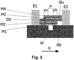
Figure 2 schematically shows, by means of a side cross-view, the electro-optical modulator of the first aspect of the present invention, for a similar embodiment to that ofFigure 1 . -
Figure 3 shows a diagram of optical transmission versus voltage, referring to the electro-optical modulator ofFigures 1 and2 (where voltage is applied between the first and second electrodes, i.e. VSD), but for different "graphene broadenings" (these terms will be described below). -
Figure 4 shows a diagram of bandwidth versus "graphene broadening", also referring to the electro-optical modulator ofFigures 1 and2 , for different contact resistivities. -
Figure 5 shows a diagram of optical transmission versus voltage, also referring to the electro-optical modulator ofFigures 1 and2 (where voltage is applied between the first and second electrodes, i.e. VSD), for different thicknesses of the top sheet (M4) of a second dielectric material. -
Figure 6 also shows a diagram of optical transmission versus voltage, also referring to the electro-optical modulator ofFigures 1 and2 (where voltage is applied between the first and second electrodes, i.e. VSD), for different thicknesses of the bottom sheet (M1) of a second dielectric material, including a case for a zero-thickness waveform, i.e. a case for the electro-optical modulator shown inFigures 1 and2 but modified so that it does not include the bottom sheet (M1). -
Figure 7 shows a diagram of optical transmission versus voltage, also referring to the electro-optical modulator ofFigures 1 and2 (where voltage is applied between the first and second electrodes, i.e. VSD), for different percentages of thickness of the sheet (DS) of a first dielectric material. -
Figure 8 shows a diagram of optical transmission versus voltage, also referring to the electro-optical modulator ofFigures 1 and2 (where voltage is applied between the first and second electrodes, i.e. VSD), for different combinations of sheets of first and second dielectric materials, and respective thicknesses, for which either the top sheet (M4) and the bottom sheet (M1) of the second dielectric material are not included, i.e. cases for the electro-optical modulator shown inFigures 1 and2 but modified so that it does not include one of said sheets (M4 or M1). -
Figure 9 shows a diagram of optical transmission versus voltage, also referring to the electro-optical modulator ofFigures 1 and2 (where voltage is applied between the first and second electrodes, i.e. VSD), for different thicknesses of whole dielectric material in between the top and bottom graphene sheets, i.e. the layers M3, M2 and DS. -
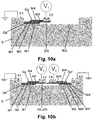
Figures 10a to 10e schematically show different variants and/or implementations of an embodiment for which the electro-optical modulator according to the first aspect of present invention implements a Mach-Zehnder interferometer based arrangement. - In the present section some working embodiments of the electro-optical modulator of the first aspect of the present invention will be described with reference to the Figures.
- Specifically, in
Figures 1 and2 embodiments for which the modulator has only one waveguide are disclosed, while inFigures 10a to 10 an embodiment for which the modulator has two waveguides is disclosed, particularly to implement different Mach-Zehnder interferometer based arrangements. - As shown in
Figures 1 and2 , for the embodiment there illustrated, the electro-optical modulator comprises: - a semiconductor substrate S, which is usually covered by a thin layer (usually of about 20nm-thin), called cladding (not shown), made of an oxide material, such as SiO2;
- first E1 and second electrodes E2 distanced from each other along an X-direction (see
Figure 2 ), and subjected to a drain-source voltage as shown inFigure 1 ; - an optical waveguide W embedded within the semiconductor substrate S with an upper face flush (although if not flush, the modulator shall also properly operate) with an upper face of the semiconductor substrate S, wherein, for the illustrated embodiment, the upper face of the optical waveguide W is located just below a location between the first E1 and second E2 electrodes, along the X-direction, wherein the optical waveguide W longitudinally extends along a direction transversal (preferably perpendicular) to the X-direction;
- a bottom graphene sheet Gb arranged and extending along the X-direction over a portion of the upper face of the semiconductor substrate S, with a first end electrically connected to the first electrode E1 and without the bottom graphene sheet Gb reaching the second electrode E2;
- a sheet DS of a first dielectric material extending over the bottom graphene sheet Gb contacting both the first E1 and the second E2 electrodes;
- a top graphene sheet Gu arranged and extending along the X-direction over a portion of the sheet DS of a first dielectric material, with a first end electrically connected to the second electrode E2 and without the top graphene sheet Gu reaching the first electrode E1; and
- a second dielectric material, with at least dielectric properties different to the dielectric properties of said first dielectric material, covering upper and bottom faces of the top graphene sheet Gu and/or an upper face or both upper and bottom faces of the bottom graphene sheet Gb.
- For the illustrated embodiment, each of the top Gu and bottom Gb graphene sheets extends along the X-direction completely above the whole width of the optical waveguide W, and beyond through a respective further projecting portion, identified with the referrals pu and pb, respectively.
- Each of those projecting portions pu, pb has a length, along the X direction, of up to 25% of the optical waveguide W width, identified with the referral "a". In
Figure 2 , those projecting portions pu, pb seem to be longer, but that's just a schematic representation which cannot be used to extract a teaching concerning a dimension from a measurement therein. Indeed, projecting portions pu and pb have a length of up to 25% the width "a". - Alternatively, for non-illustrated embodiments, each of the top Gu and bottom Gb graphene sheets extends along the X-direction above only part of the width of the optical waveguide W, particularly above a part which ranges from 50% to 100% of the width "a" of the optical waveguide W.
- In the present document, and particularly in the diagrams of
Figures 3 and4 , the terms "graphene broadening" has been used to refer to the above described extension along the X-direction of the top Gu and bottom Gb graphene sheets, although in this case in absolute terms (i.e. not by means of percentages), for a width "a" for the optical waveguide W of 1 µm. - Particularly, positive values for the "graphene broadening" correspond to values of the above mentioned length of each of the projecting portions pu and pb. A waveform with a "graphene broadening" of 1000 nm (i.e. for a projecting portion with a length of 100% the width "a") is shown which is not part of the present invention, but depicted only for comparison purposes with the rest of waveforms.
- The "graphene broadening" negative values refer to the above described embodiment for which each of the top Gu and bottom Gb graphene sheets extends along the X-direction above only part ranging from 50% to 100% of the width a of the optical waveguide W. Particularly, each negative value correspond to a length value, measured along the X-direction, of the distance existing between the free edge of the corresponding graphene sheet (top Gu or bottom Gb) and the edge of the waveguide W towards which the graphene sheet is extending but does not arrive to. In other words, for a width "a" of 1 µm, a "graphene broadening" of -225 nm corresponds with a part of a 77.5% of the width "a" along which the corresponding graphene sheet extend along the X-direction.
- By comparing the results of the diagrams of
Figures 3 and4 , one can see how slightly varying the "graphene broadening" has a great impact in the increase of the operating optical bandwidth while the optical transmission is only slightly reduced. - The present inventors have discovered that this is due to the fact that the region where the top Gu and bottom Gb graphene sheets overlap has a capacitance C that is directly proportional to its dimensions. The bandwidth of the modulator is defined as BW = 1/ 2πRC. The smaller the overlap between the top Gu and bottom Gb graphene sheets, the lower the C, thus increasing the bandwidth (this is directly seen in
Figure 4 ). From the other side, a lower C, i.e. a lower overlapped region, will have a worst transmission (as seenFigure 3 ). - The diagrams of
Figures 3 and4 , and also those ofFigures 5 ,6 ,7 and8 , have been obtained from numerical simulations for an electro-optical modulator for which the first dielectric material is HfO2 and the second electro-optical material is hBN. However, similar results can be obtained for other types of dielectric materials, such as for those cited in a previous section of this document. - For the embodiment illustrated in
Figures 1 and2 : - top M4 and bottom M3 sheets of the second dielectric material sandwich the top graphene sheet Gu, contact the second electrode E2 and extend, along the X-direction, up to at least just above and just below, respectively, a top graphene Gu free edge, and
- top M2 and a bottom M1 sheets of the second dielectric material sandwiching the bottom graphene sheet Gb, contact the first electrode E1 and extend, along the X-direction, up to just above and just below, respectively, a bottom graphene Gb free edge.
- The diagrams of
Figures 5 and6 respectively show the effect of the top sheet M4 thickness and of the bottom sheet M1 thickness (including a zero-thickness M1 sheet case). The results illustrated in those diagrams show that, for the M4 top sheet, the thicker the better, and that for the M1 bottom sheet, the thinner the better. - The influence of the thickness of the sheet DS of a first dielectric material is shown in
Figure 7 , for which the first dielectric material is HfO2. The total thickness of the dielectric sheets (all of them, the ones of the first dielectric material and the ones of the second dielectric material) has been kept constant, so that when the thickness of HfO2 has been increased, the thickness of the M2 and/or M3 sheets has been proportionally reduced. The results show how for the DS sheet, the higher percentage the better. -
Figure 8 shows how the order of the different dielectric sheets within the top and bottom graphene sheets (only M3, M2 and DS have been taken into account) has no influence in the optical transmission. This is due to the fact that, for the simulations, M1 and M2 are the same materials and what matters is their total thickness. - The influence of the thickness of dielectric material within the top and bottom graphene sheets (M3+M2+DS) is shown in
Figure 9 , showing that the smaller the thickness the better. The relative thickness (percentage) of each dielectric sheet has been kept constant. - The influence of the thickness of the whole dielectric material (M1+M2+M3+M4+DS) is shown in
Figure 9 , showing that the higher the thickness, the better. The relative thickness (percentage) of each dielectric sheet has been kept constant. -
Figures 10a to 10e schematically show different variants and/or implementations of an embodiment for which the electro-optical modulator according to the first aspect of present invention implements a Mach-Zehnder interferometer based arrangement, wherein the optical waveguide W is a first optical waveguide branch W1, and the modulator further comprises: - a second optical waveguide branch W2 distanced from the first optical waveguide branch W1 along the X-direction and embedded within the semiconductor substrate S, wherein the second optical waveguide branch W2 longitudinally extends along at least the direction transversal to the X-direction; and
- a third electrode E3 located distanced from the second electrode E2 along the X-direction, wherein, for the illustrated embodiment the upper face of the second optical waveguide branch W2 is located below a location between said second E2 and third electrodes E3, along the X-direction.
- For the variant shown in
Figure 10a , the second optical waveguide branch W2 is left uncovered, just embedded within the substrate S. Therefore, in use, i.e. when a voltage V1 is applied between the first E1 and the second E2 electrodes, only the phase of the light travelling through the core of the first optical waveguide branch W1 is changed. - For the rest of variant, i.e. for those of
Figures 10b to 10e , in use, the phase of the light travelling through the cores of both optical waveguide branches, W1 and W2, is changed, and the electro-optical modulator further comprises: - a further bottom graphene sheet Gbf arranged and extending, along the X-direction, over at least a portion of the upper face of the semiconductor substrate S and over at least a portion of the second optical waveguide branch W2;
- a further sheet DSf of said first dielectric material extending along the X-direction over the further bottom graphene sheet Gbf;
- a further top graphene sheet Guf arranged and extending along the X-direction over at least a portion of the further sheet DSf of the first dielectric material and over at least a portion of the second optical waveguide branch W2; and
- further portions of the second dielectric material covering upper and bottom faces of said further top graphene sheet Guf and/or an upper face or upper and bottom faces of said further bottom graphene sheet Gbf.
- One or both of the further top Guf and further bottom Gbf graphene sheets extends along the X-direction:
- above part of the width of the second optical waveguide branch W2, wherein said part ranges from 50% to 100% of the width of the second optical waveguide branch W2; or
- completely above the whole width of the second optical waveguide branch W2, and beyond through a respective further projecting portion with a length, along the X direction, of up to 25% of the width of the second optical waveguide branch W2.
- Specifically, for the variant illustrated by
Figures 10b and10c : - the further bottom graphene sheet Gbf has a first end electrically connected to the third electrode E3 and extends therefrom along the X-direction, over only a portion of the upper face of the semiconductor substrate S and, in this case, above the whole width of the second optical waveguide branch W2 and beyond through a respective further projecting portion with a length, along the X direction, of up to 25% of the width of second optical waveguide branch W2, although, as stated above, it could extend above only a part ranging from 50% to 100% of that width;
- said further sheet DSf of said first dielectric material is integral with said sheet DS of said first dielectric material; and
- said further top graphene sheet Guf has a first end electrically connected to the second electrode E2 and extends therefrom along the X-direction without reaching the third electrode E3, in this case, above the whole width of the second optical waveguide branch W2 and beyond (up to 25% its width), although, as stated above, it could extend above only a part ranging from 50% to 100% of that width.
- Alternatively, for a non-illustrated embodiment, each of the top Gu and bottom Gb graphene sheets extends along the X-direction above only part of the width of the second optical waveguide branch W2, particularly above a part which ranges from 50% to 100% of the width of the second optical waveguide branch W2.
- The differences between the variants of
Figures 10b and10c are just the electrodes to which the terminals of voltage source V1 is applied, as voltage source V2 is applied to the same electrodes for both figures. ForFigure 10b , voltage V1 is applied to the second electrode E2 while the first E1 electrode is connected to ground, and forFigure 10c the inverse connection is made. - For the variant illustrated by
Figure 10d , the electro-optical modulator further comprises a fourth electrode E4 located between the second E2 and third E3 electrodes along the X-direction, wherein the upper face of the second optical waveguide branch W2 is located below a location between the fourth E4 and third electrodes E3, along the X-direction; and wherein: - the further bottom graphene sheet Gbf is integral with the bottom graphene sheet Gb, so that opposite ends of the resulting common graphene sheet are respectively electrically connected to the first E1 and the third E3 electrode, extending along the X-direction over the upper face of the substrate S and above the whole width of both the first W and the second W2 optical waveguide branches;
- the further sheet DSf of the first dielectric material is integral with the sheet DS of the first dielectric material; and
- the further top graphene sheet Guf has a first end electrically connected to the fourth electrode E4 and extends therefrom along the X-direction without reaching the third electrode E3, in this case above the whole width of the second optical waveguide branch W2 and beyond (up to 25% its width), although, as stated above, it could extend above only a part ranging from 50% to 100% of that width.
- For the variant of
Figure 10d , the voltage sources V1 and V2 are connected the same as for that ofFigure 10b . - As shown in
Figure 10e , for the variant there illustrated: - the further bottom graphene sheet Gbf has a first end electrically connected to the third electrode E3 and extends therefrom along the X-direction, over a portion of the upper face of the semiconductor substrate S, and, in this case, above the whole width of the second optical waveguide branch W2 and beyond (up to 25% its width), although, as stated above, it could extend above only a part ranging from 50% to 100% of that width;
- the further sheet DSf of the first dielectric material is integral with the sheet DS of the first dielectric material and the resulting common sheets extends from the first E1 to the third E3 electrodes; and
- the further top graphene sheet Guf is integral with the top graphene sheet Gu, so a central region of the resulting common graphene sheet is electrically connected to the second electrode E2, and both opposite ends extend, along the X-direction over the upper face of the substrate S, towards the first E1 and the third E3 electrodes, respectively, so that, in this case, each, Gu and Guf, extends above the whole width of the first W1 or second W2 optical waveguide branch and beyond (up to 25% its width), although, as stated above, it could extend above only a part ranging from 50% to 100% of that width.
- For the variant of
Figure 10e , three voltages are applied, namely V1, V2 and V3, each to a respective of the first E1, second E2 and third E3 electrodes. - As state above,
Figures 10a to 10e are schematic, which means, for example, that those elements depicted floating are not floating but really bent. - The operation of the modulators of
Figures 10a to 10e is the already known associated to Mach-Zehnder interferometer based arrangements together with the one already explained above for the modulator ofFigures 1 and2 , i.e. it benefits from the same effects explained above with respect to the "graphene broadening". - A person skilled in the art could introduce changes and modifications in the embodiments described without departing from the scope of the invention as it is defined in the attached claims.
Claims (15)
- An electro-optical modulator, comprising:- a semiconductor substrate (S);- at least first (E1) and second electrodes (E2) distanced from each other along an X-direction;- an optical waveguide (W) embedded within and/or arranged on said semiconductor substrate (S), an upper face of said optical waveguide (W) being located at, below or above a location between said first (E1) and second (E2) electrodes, along said X-direction, wherein said optical waveguide (W) longitudinally extends along at least a direction transversal to said X-direction;- a bottom graphene sheet (Gb) arranged and extending along said X-direction over at least a portion of the upper face of the semiconductor substrate (S), with a first end electrically connected to said first electrode (E1) and without the bottom graphene sheet (Gb) reaching the second electrode (E2);- a sheet (DS) of a first dielectric material extending over said bottom graphene sheet (Gb);- a top graphene sheet (Gu) arranged and extending along said X-direction over at least a portion of said sheet (DS) of a first dielectric material, with a first end electrically connected to said second electrode (E2) and without the top graphene sheet (Gu) reaching the first electrode (E1); and- a second dielectric material, which is a two-dimensional material with at least dielectric properties different to the dielectric properties of said first dielectric material, covering upper and bottom faces of said top graphene sheet (Gu) and/or an upper face or both upper and bottom faces of said bottom graphene sheet (Gb);characterized in that at least one of said top (Gu) and bottom (Gb) graphene sheets extends along said X-direction:- above part of the width of the optical waveguide (W), wherein said part ranges from 50% to 100% of the width of the optical waveguide (W); or- completely above the whole width of the optical waveguide (W), and beyond through a respective further projecting portion with a length, along the X direction, of up to 25% of the optical waveguide (W) width.
- The electro-optical modulator according to claim 1, wherein each of the top (Gu) and bottom (Gb) graphene sheets extends along the X-direction:- above part of the width of the optical waveguide (W), wherein said part ranges from 50% to 100% of the width of the optical waveguide (W); or- completely above the whole width of the optical waveguide (W), and beyond through a respective further projecting portion with a length, along the X direction, of up to 25% of the optical waveguide (W) width.
- The electro-optical modulator according to claim 1 or 2, wherein at least one of the top (Gu) and bottom (Gb) graphene sheets extends along said X-direction from a 75% to a 100% above the optical waveguide (W) width, or completely above the optical waveguide (W) width and beyond through a further projecting portion with a length of up to a 25% of the optical waveguide (W) width.
- The electro-optical modulator according to claim 3, wherein at least one of the top (Gu) and bottom (Gb) graphene sheets extend along said X-direction from a 95% to a 100% above the optical waveguide (W) width, or completely above the optical waveguide (W) width and beyond through a further projecting portion with a length of up to a 5% of the optical waveguide (W) width.
- The electro-optical modulator according to any of the previous claims, wherein:- said sheet (DS) of a first dielectric material extends along the X-direction at least within an area overlapped by both the top (Gu) and the bottom (Gb) graphene sheets s; and- a bottom sheet (M3) of said second dielectric material covering the lower face of the top graphene sheet (Gu) or a top (M4) and bottom (M3) sheets sandwiching the top graphene sheet (Gu), contact the second electrode (E2) and extend, along the X-direction, up to at least just above and just below, respectively, a top graphene (Gu) free edge, and/or- a top sheet (M2) of said second dielectric material covering the upper face of the bottom graphene sheet (Gb) or a top (M2) and a bottom (M1) sheets of the second dielectric material sandwiching the bottom graphene sheet (Gb), contact the first electrode (E1) and extend, along the X-direction, up to at least just above or just above and just below, respectively, a bottom graphene (Gb) free edge.
- The electro-optical modulator according to claim 5, wherein, regarding the different sheets of the second dielectric material:- the thickness of the top sheet (M4) sandwiching, together with the bottom sheet (M3), the top graphene sheet (Gu), ranges from 0 to 200 nm;- the thickness of the bottom (M1) sheet sandwiching, together with the top sheet (M2), the bottom graphene sheet (Gb), ranges from 0 nm to 10 nm; and- the thickness of the bottom sheet (M3) sandwiching, together with the top sheet (M4), the top graphene sheet (GU), added to the thickness of the top sheet (M2) sandwiching, together with the bottom sheet (M1), the bottom graphene sheet (Gb), ranges from 2 nm to 40 nm.
- The electro-optical modulator according to any of the previous claims, wherein the total dielectric thickness, including the thickness of the sheet (DS) of a first dielectric material and the thickness of the second dielectric material, ranges from 9 nm to 30 nm.
- The electro-optical modulator according to any of the previous claims, wherein the thickness of the sheet (DS) of a first dielectric material ranges from a 10% to a 200% with respect to the thickness of the second dielectric material.
- The electro-optical modulator according to any of the previous claims, wherein:- said first dielectric material is at least one of the following materials, or a combination thereof: HfO2, SiO2, Si3N4, Al2O3, ZrO2, TiO2, TiN, HfSiO4, ZrSiO4, Calcium Copper Titanate, Barium Titanate, Strontium Titanate, Barium Strontium Titanate, Polystyrene, Polypropylene, Polyiamide, Polyethylene, and Polytetrafluoroethylene; and- said second dielectric material is at least one of the following 2D layered materials, or a combination thereof: hBN, MoTe2, WSe2, WS2, graphene, MoS2, MoSe2, WS2, WSe2, black phosphorus, and SnS2.
- The electro-optical modulator according to any of the previous claims, which implements a Mach-Zehnder interferometer based arrangement, wherein said optical waveguide (W) is a first optical waveguide branch (W1), the modulator further comprising:- a second optical waveguide branch (W2) distanced from the first optical waveguide branch (W1) along the X-direction and embedded within and/or arranged on the semiconductor substrate (S), wherein said second optical waveguide branch (W2) longitudinally extends along at least the direction transversal to the X-direction; and- a third electrode (E3) located distanced from the second electrode (E2) along the X-direction, wherein the upper face of said second optical waveguide branch (W2) is located at, below or above a location between said second (E2) and third electrodes (E3), along said X-direction.
- The electro-optical modulator according to claim 10, further comprising:- a further bottom graphene sheet (Gbf) arranged and extending, along the X-direction, over at least a portion of the upper face of the semiconductor substrate (S) and over at least a portion of the second optical waveguide branch (W2);- a further sheet (DSf) of said first dielectric material extending along the X-direction over the further bottom graphene sheet (Gbf);- a further top graphene sheet (Guf) arranged and extending along said X-direction over at least a portion of the further sheet (DSf) of said first dielectric material and over at least a portion of the second optical waveguide branch (W2); and- further portions of the second dielectric material covering upper and bottom faces of said further top graphene sheet (Guf) and/or an upper face or upper and bottom faces of said further bottom graphene sheet (Gbf);wherein at least one of said further top (Guf) and further bottom (Gbf) graphene sheets extends along said X-direction:- above part of the width of the second optical waveguide branch (W2), wherein said part ranges from 50% to 100% of the width of the second optical waveguide branch (W2); or- completely above the whole width of the second optical waveguide branch (W2), and beyond through a respective further projecting portion with a length, along the X direction, of up to 25% of the width of the second optical waveguide branch (W2).
- The electro-optical modulator according to claim 11, wherein:- said further bottom graphene sheet (Gbf) has a first end electrically connected to the third electrode (E3) and extends therefrom along the X-direction, over at least said portion of the upper face of the semiconductor substrate (S) and over at least said portion of the second optical waveguide branch (W2);- said further sheet (DSf) of said first dielectric material is integral with said sheet (DS) of said first dielectric material; and- said further top graphene sheet (Guf) has a region electrically connected to the second electrode (E2) and extends therefrom along the X-direction without reaching the third electrode (E3).
- The electro-optical modulator according to claim 11, further comprising a fourth electrode (E4) located between the second (E2) and third (E3) electrodes along the X-direction, wherein the upper face of the second optical waveguide branch (W2) is located at, below or above a location between said fourth (E4) and third electrodes (E3), along the X-direction; and wherein:- said further bottom graphene sheet (Gbf) has a first end electrically connected to the third electrode (E3) and extends therefrom along the X-direction, over at least said portion of the upper face of the semiconductor substrate (S) and over at least said portion of the second optical waveguide branch (W2);- said further sheet (DSf) of said first dielectric material is integral with said sheet (DS) of said first dielectric material; and- said further top graphene sheet (Guf) has a first end electrically connected to the fourth electrode (E4) and extends therefrom along the X-direction without reaching the third electrode (E3).
- A method for obtaining an electro-optical modulator, comprising providing and arranging each of the components of the electro-optical modulator according to any of the previous claims.
- The method according to claim 14, comprising using a criterion based on requirements of target optical bandwidth and target optical transmission to be met by the electro-optical modulator, to determine the lengths to be provided to:- at least one of the top (Gu) and bottom (Gb) graphene sheets to respectively extend along the X-direction above the optical waveguide (W) width, or completely above the whole width of the optical waveguide (W) and beyond through a respective further projecting portion, and/or,- at least one of the further top (Guf) and further (Gbf) bottom graphene sheets to respectively extend along the X-direction above the width of the second optical waveguide branch (W2), or completely above the whole width of the second optical waveguide branch (W2) and beyond through a respective further projecting portion.
Priority Applications (3)
| Application Number | Priority Date | Filing Date | Title |
|---|---|---|---|
| EP19383089.0A EP3832381B1 (en) | 2019-12-05 | 2019-12-05 | An electro-optical modulator and a method for obtaining an electro-optical modulator. |
| US17/113,749 US11860502B2 (en) | 2019-12-05 | 2020-12-07 | Electro-optical modulator and a method for obtaining an electro-optical modulator |
| CN202011430192.1A CN112925123B (en) | 2019-12-05 | 2020-12-07 | Electro-optical modulator and method for obtaining the same |
Applications Claiming Priority (1)
| Application Number | Priority Date | Filing Date | Title |
|---|---|---|---|
| EP19383089.0A EP3832381B1 (en) | 2019-12-05 | 2019-12-05 | An electro-optical modulator and a method for obtaining an electro-optical modulator. |
Publications (2)
| Publication Number | Publication Date |
|---|---|
| EP3832381A1 true EP3832381A1 (en) | 2021-06-09 |
| EP3832381B1 EP3832381B1 (en) | 2025-07-23 |
Family
ID=69061240
Family Applications (1)
| Application Number | Title | Priority Date | Filing Date |
|---|---|---|---|
| EP19383089.0A Active EP3832381B1 (en) | 2019-12-05 | 2019-12-05 | An electro-optical modulator and a method for obtaining an electro-optical modulator. |
Country Status (3)
| Country | Link |
|---|---|
| US (1) | US11860502B2 (en) |
| EP (1) | EP3832381B1 (en) |
| CN (1) | CN112925123B (en) |
Families Citing this family (2)
| Publication number | Priority date | Publication date | Assignee | Title |
|---|---|---|---|---|
| CN114063203B (en) * | 2021-11-11 | 2023-12-12 | 浙江传媒学院 | Surface plasmon optical modulator and photoelectric device |
| WO2024218259A1 (en) | 2023-04-20 | 2024-10-24 | Blacklink Technologies, S.L. | Electro-optic modulators and methods of operation |
Citations (7)
| Publication number | Priority date | Publication date | Assignee | Title |
|---|---|---|---|---|
| WO2012145605A1 (en) * | 2011-04-22 | 2012-10-26 | The Regents Of The University Of California | Graphene based optical modulator |
| EP2584397A1 (en) * | 2011-10-19 | 2013-04-24 | Samsung Electronics Co., Ltd. | Optical electro-absorption modulator including two graphene sheets |
| CN105700203A (en) * | 2016-04-26 | 2016-06-22 | 电子科技大学 | Planar waveguide type near-and-mid infrared light modulator based on graphene-chalcogenide glass |
| CN106980189A (en) * | 2017-06-02 | 2017-07-25 | 电子科技大学 | Graphene microstrip line traveling wave absorption-type optical modulator based on strip optical waveguide |
| CN107037613A (en) * | 2017-06-02 | 2017-08-11 | 电子科技大学 | The M Z electrooptic modulators with adjustable grating based on graphene molybdenum disulfide hetero-junctions |
| CN105068279B (en) * | 2015-08-04 | 2018-02-16 | 电子科技大学 | A kind of polarization insensitive optical modulator based on arc graphene |
| CN107153280B (en) * | 2017-06-29 | 2019-05-10 | 电子科技大学 | An Absorption Optical Modulator Based on Graphene Coplanar Traveling Wave Electrode |
Family Cites Families (7)
| Publication number | Priority date | Publication date | Assignee | Title |
|---|---|---|---|---|
| JP2017011209A (en) * | 2015-06-25 | 2017-01-12 | 株式会社東芝 | Graphene light receiving element and graphene light modulator |
| JP6062496B1 (en) * | 2015-06-26 | 2017-01-18 | 株式会社フジクラ | Optical waveguide device |
| CN105022178B (en) * | 2015-08-18 | 2018-04-03 | 电子科技大学 | Graphene phase type optical modulator based on slab guide |
| CN106526904A (en) * | 2016-12-06 | 2017-03-22 | 深圳大学 | Graphene electro-optical modulator based on planar hybridized waveguide |
| US10775651B2 (en) * | 2017-08-25 | 2020-09-15 | The Regents Of The University Of California | Double-layer graphene optical modulators and methods of fabrication thereof |
| CN108181735A (en) * | 2017-12-25 | 2018-06-19 | 武汉邮电科学研究院 | A kind of graphene electro-optical modulator and preparation method thereof |
| CN109387956B (en) * | 2018-11-14 | 2020-09-15 | 北京邮电大学 | Graphene electro-optic modulator based on slit waveguide |
-
2019
- 2019-12-05 EP EP19383089.0A patent/EP3832381B1/en active Active
-
2020
- 2020-12-07 US US17/113,749 patent/US11860502B2/en active Active
- 2020-12-07 CN CN202011430192.1A patent/CN112925123B/en active Active
Patent Citations (7)
| Publication number | Priority date | Publication date | Assignee | Title |
|---|---|---|---|---|
| WO2012145605A1 (en) * | 2011-04-22 | 2012-10-26 | The Regents Of The University Of California | Graphene based optical modulator |
| EP2584397A1 (en) * | 2011-10-19 | 2013-04-24 | Samsung Electronics Co., Ltd. | Optical electro-absorption modulator including two graphene sheets |
| CN105068279B (en) * | 2015-08-04 | 2018-02-16 | 电子科技大学 | A kind of polarization insensitive optical modulator based on arc graphene |
| CN105700203A (en) * | 2016-04-26 | 2016-06-22 | 电子科技大学 | Planar waveguide type near-and-mid infrared light modulator based on graphene-chalcogenide glass |
| CN106980189A (en) * | 2017-06-02 | 2017-07-25 | 电子科技大学 | Graphene microstrip line traveling wave absorption-type optical modulator based on strip optical waveguide |
| CN107037613A (en) * | 2017-06-02 | 2017-08-11 | 电子科技大学 | The M Z electrooptic modulators with adjustable grating based on graphene molybdenum disulfide hetero-junctions |
| CN107153280B (en) * | 2017-06-29 | 2019-05-10 | 电子科技大学 | An Absorption Optical Modulator Based on Graphene Coplanar Traveling Wave Electrode |
Also Published As
| Publication number | Publication date |
|---|---|
| US20210173281A1 (en) | 2021-06-10 |
| US11860502B2 (en) | 2024-01-02 |
| CN112925123B (en) | 2025-08-26 |
| CN112925123A (en) | 2021-06-08 |
| EP3832381B1 (en) | 2025-07-23 |
Similar Documents
| Publication | Publication Date | Title |
|---|---|---|
| US12560831B2 (en) | Electro-optical modulator using waveguides with overlapping ridges | |
| EP3832381B1 (en) | An electro-optical modulator and a method for obtaining an electro-optical modulator. | |
| EP3230793B1 (en) | Electro-optic modulator termination | |
| KR102519567B1 (en) | Signal Isolator Integrated Circuit Package | |
| CN107924075A (en) | Optical modulator | |
| JP2021524924A5 (en) | ||
| US20170075148A1 (en) | Integrated electro-optic modulator | |
| CN111051970A (en) | Optical modulator | |
| US4871223A (en) | Arrangement comprising at least one integrated optical waveguide on a substrate of electro-optical material and comprising at least one electrode | |
| JP2008171005A (en) | Moisture resistant electro-optic device | |
| JP5462837B2 (en) | Optical device or light modulator | |
| US20180017839A1 (en) | Optical modulator | |
| CN105511119A (en) | Doping structure of silicon-substrate electrooptical modulator | |
| JP2023517900A5 (en) | ||
| US6845183B2 (en) | Slotted electrode electro-optic modulator | |
| CN113467109A (en) | Optical modulator | |
| CN110989211A (en) | Monolithic electro-optic modulator with comb-shaped transmission lines | |
| US20230112785A1 (en) | Electro-optical device | |
| WO2013147129A1 (en) | Optical waveguide element | |
| US20100260461A1 (en) | Waveguide type optical device | |
| CN108107608A (en) | A kind of electrooptic modulator of the polarization insensitive based on transparent conductive oxide | |
| EP4399565A1 (en) | Optical modulator including a graphene layer and method for modulating an electromagnetic radiation | |
| WO2014040981A1 (en) | Soi finfet with reduced fin width dependence | |
| US9151971B2 (en) | Liquid crystal lens and stereoscopic display device | |
| WO2012102272A1 (en) | Light-polarizing element |
Legal Events
| Date | Code | Title | Description |
|---|---|---|---|
| PUAI | Public reference made under article 153(3) epc to a published international application that has entered the european phase |
Free format text: ORIGINAL CODE: 0009012 |
|
| STAA | Information on the status of an ep patent application or granted ep patent |
Free format text: STATUS: THE APPLICATION HAS BEEN PUBLISHED |
|
| AK | Designated contracting states |
Kind code of ref document: A1 Designated state(s): AL AT BE BG CH CY CZ DE DK EE ES FI FR GB GR HR HU IE IS IT LI LT LU LV MC MK MT NL NO PL PT RO RS SE SI SK SM TR |
|
| STAA | Information on the status of an ep patent application or granted ep patent |
Free format text: STATUS: REQUEST FOR EXAMINATION WAS MADE |
|
| 17P | Request for examination filed |
Effective date: 20211209 |
|
| RBV | Designated contracting states (corrected) |
Designated state(s): AL AT BE BG CH CY CZ DE DK EE ES FI FR GB GR HR HU IE IS IT LI LT LU LV MC MK MT NL NO PL PT RO RS SE SI SK SM TR |
|
| STAA | Information on the status of an ep patent application or granted ep patent |
Free format text: STATUS: EXAMINATION IS IN PROGRESS |
|
| 17Q | First examination report despatched |
Effective date: 20230509 |
|
| GRAP | Despatch of communication of intention to grant a patent |
Free format text: ORIGINAL CODE: EPIDOSNIGR1 |
|
| STAA | Information on the status of an ep patent application or granted ep patent |
Free format text: STATUS: GRANT OF PATENT IS INTENDED |
|
| GRAS | Grant fee paid |
Free format text: ORIGINAL CODE: EPIDOSNIGR3 |
|
| GRAA | (expected) grant |
Free format text: ORIGINAL CODE: 0009210 |
|
| STAA | Information on the status of an ep patent application or granted ep patent |
Free format text: STATUS: THE PATENT HAS BEEN GRANTED |
|
| INTG | Intention to grant announced |
Effective date: 20250528 |
|
| AK | Designated contracting states |
Kind code of ref document: B1 Designated state(s): AL AT BE BG CH CY CZ DE DK EE ES FI FR GB GR HR HU IE IS IT LI LT LU LV MC MK MT NL NO PL PT RO RS SE SI SK SM TR |
|
| REG | Reference to a national code |
Ref country code: GB Ref legal event code: FG4D |
|
| REG | Reference to a national code |
Ref country code: CH Ref legal event code: EP |
|
| REG | Reference to a national code |
Ref country code: IE Ref legal event code: FG4D |
|
| REG | Reference to a national code |
Ref country code: DE Ref legal event code: R096 Ref document number: 602019072847 Country of ref document: DE |
|
| REG | Reference to a national code |
Ref country code: NL Ref legal event code: MP Effective date: 20250723 |
|
| PG25 | Lapsed in a contracting state [announced via postgrant information from national office to epo] |
Ref country code: PT Free format text: LAPSE BECAUSE OF FAILURE TO SUBMIT A TRANSLATION OF THE DESCRIPTION OR TO PAY THE FEE WITHIN THE PRESCRIBED TIME-LIMIT Effective date: 20251124 |
|
| PG25 | Lapsed in a contracting state [announced via postgrant information from national office to epo] |
Ref country code: NL Free format text: LAPSE BECAUSE OF FAILURE TO SUBMIT A TRANSLATION OF THE DESCRIPTION OR TO PAY THE FEE WITHIN THE PRESCRIBED TIME-LIMIT Effective date: 20250723 |
|
| REG | Reference to a national code |
Ref country code: AT Ref legal event code: MK05 Ref document number: 1817006 Country of ref document: AT Kind code of ref document: T Effective date: 20250723 |
|
| PG25 | Lapsed in a contracting state [announced via postgrant information from national office to epo] |
Ref country code: IS Free format text: LAPSE BECAUSE OF FAILURE TO SUBMIT A TRANSLATION OF THE DESCRIPTION OR TO PAY THE FEE WITHIN THE PRESCRIBED TIME-LIMIT Effective date: 20251123 |
|
| PGFP | Annual fee paid to national office [announced via postgrant information from national office to epo] |
Ref country code: DE Payment date: 20251210 Year of fee payment: 7 |
|
| PGFP | Annual fee paid to national office [announced via postgrant information from national office to epo] |
Ref country code: GB Payment date: 20251211 Year of fee payment: 7 |
|
| PG25 | Lapsed in a contracting state [announced via postgrant information from national office to epo] |
Ref country code: NO Free format text: LAPSE BECAUSE OF FAILURE TO SUBMIT A TRANSLATION OF THE DESCRIPTION OR TO PAY THE FEE WITHIN THE PRESCRIBED TIME-LIMIT Effective date: 20251023 |
|
| REG | Reference to a national code |
Ref country code: LT Ref legal event code: MG9D |
|
| PG25 | Lapsed in a contracting state [announced via postgrant information from national office to epo] |
Ref country code: AT Free format text: LAPSE BECAUSE OF FAILURE TO SUBMIT A TRANSLATION OF THE DESCRIPTION OR TO PAY THE FEE WITHIN THE PRESCRIBED TIME-LIMIT Effective date: 20250723 |
|
| PG25 | Lapsed in a contracting state [announced via postgrant information from national office to epo] |
Ref country code: FI Free format text: LAPSE BECAUSE OF FAILURE TO SUBMIT A TRANSLATION OF THE DESCRIPTION OR TO PAY THE FEE WITHIN THE PRESCRIBED TIME-LIMIT Effective date: 20250723 |
|
| PGFP | Annual fee paid to national office [announced via postgrant information from national office to epo] |
Ref country code: IT Payment date: 20251219 Year of fee payment: 7 |
|
| PG25 | Lapsed in a contracting state [announced via postgrant information from national office to epo] |
Ref country code: HR Free format text: LAPSE BECAUSE OF FAILURE TO SUBMIT A TRANSLATION OF THE DESCRIPTION OR TO PAY THE FEE WITHIN THE PRESCRIBED TIME-LIMIT Effective date: 20250723 |
|
| PG25 | Lapsed in a contracting state [announced via postgrant information from national office to epo] |
Ref country code: GR Free format text: LAPSE BECAUSE OF FAILURE TO SUBMIT A TRANSLATION OF THE DESCRIPTION OR TO PAY THE FEE WITHIN THE PRESCRIBED TIME-LIMIT Effective date: 20251024 |
|
| PG25 | Lapsed in a contracting state [announced via postgrant information from national office to epo] |
Ref country code: SE Free format text: LAPSE BECAUSE OF FAILURE TO SUBMIT A TRANSLATION OF THE DESCRIPTION OR TO PAY THE FEE WITHIN THE PRESCRIBED TIME-LIMIT Effective date: 20250723 |
|
| PG25 | Lapsed in a contracting state [announced via postgrant information from national office to epo] |
Ref country code: LV Free format text: LAPSE BECAUSE OF FAILURE TO SUBMIT A TRANSLATION OF THE DESCRIPTION OR TO PAY THE FEE WITHIN THE PRESCRIBED TIME-LIMIT Effective date: 20250723 |
|
| PG25 | Lapsed in a contracting state [announced via postgrant information from national office to epo] |
Ref country code: BG Free format text: LAPSE BECAUSE OF FAILURE TO SUBMIT A TRANSLATION OF THE DESCRIPTION OR TO PAY THE FEE WITHIN THE PRESCRIBED TIME-LIMIT Effective date: 20250723 Ref country code: PL Free format text: LAPSE BECAUSE OF FAILURE TO SUBMIT A TRANSLATION OF THE DESCRIPTION OR TO PAY THE FEE WITHIN THE PRESCRIBED TIME-LIMIT Effective date: 20250723 |
|
| PG25 | Lapsed in a contracting state [announced via postgrant information from national office to epo] |
Ref country code: RS Free format text: LAPSE BECAUSE OF FAILURE TO SUBMIT A TRANSLATION OF THE DESCRIPTION OR TO PAY THE FEE WITHIN THE PRESCRIBED TIME-LIMIT Effective date: 20251023 |
|
| PG25 | Lapsed in a contracting state [announced via postgrant information from national office to epo] |
Ref country code: ES Free format text: LAPSE BECAUSE OF FAILURE TO SUBMIT A TRANSLATION OF THE DESCRIPTION OR TO PAY THE FEE WITHIN THE PRESCRIBED TIME-LIMIT Effective date: 20250723 |
|
| PG25 | Lapsed in a contracting state [announced via postgrant information from national office to epo] |
Ref country code: RO Free format text: LAPSE BECAUSE OF FAILURE TO SUBMIT A TRANSLATION OF THE DESCRIPTION OR TO PAY THE FEE WITHIN THE PRESCRIBED TIME-LIMIT Effective date: 20250723 |
|
| PG25 | Lapsed in a contracting state [announced via postgrant information from national office to epo] |
Ref country code: SM Free format text: LAPSE BECAUSE OF FAILURE TO SUBMIT A TRANSLATION OF THE DESCRIPTION OR TO PAY THE FEE WITHIN THE PRESCRIBED TIME-LIMIT Effective date: 20250723 |
|
| PG25 | Lapsed in a contracting state [announced via postgrant information from national office to epo] |
Ref country code: DK Free format text: LAPSE BECAUSE OF FAILURE TO SUBMIT A TRANSLATION OF THE DESCRIPTION OR TO PAY THE FEE WITHIN THE PRESCRIBED TIME-LIMIT Effective date: 20250723 |
|
| PG25 | Lapsed in a contracting state [announced via postgrant information from national office to epo] |
Ref country code: CZ Free format text: LAPSE BECAUSE OF FAILURE TO SUBMIT A TRANSLATION OF THE DESCRIPTION OR TO PAY THE FEE WITHIN THE PRESCRIBED TIME-LIMIT Effective date: 20250723 |
|
| PG25 | Lapsed in a contracting state [announced via postgrant information from national office to epo] |
Ref country code: SK Free format text: LAPSE BECAUSE OF FAILURE TO SUBMIT A TRANSLATION OF THE DESCRIPTION OR TO PAY THE FEE WITHIN THE PRESCRIBED TIME-LIMIT Effective date: 20250723 Ref country code: EE Free format text: LAPSE BECAUSE OF FAILURE TO SUBMIT A TRANSLATION OF THE DESCRIPTION OR TO PAY THE FEE WITHIN THE PRESCRIBED TIME-LIMIT Effective date: 20250723 |