EP3831524A1 - Information processing device, management system, control program, and method for controlling information processing device - Google Patents
Information processing device, management system, control program, and method for controlling information processing device Download PDFInfo
- Publication number
- EP3831524A1 EP3831524A1 EP19843824.4A EP19843824A EP3831524A1 EP 3831524 A1 EP3831524 A1 EP 3831524A1 EP 19843824 A EP19843824 A EP 19843824A EP 3831524 A1 EP3831524 A1 EP 3831524A1
- Authority
- EP
- European Patent Office
- Prior art keywords
- jet
- solder
- soldering device
- shape
- state
- Prior art date
- Legal status (The legal status is an assumption and is not a legal conclusion. Google has not performed a legal analysis and makes no representation as to the accuracy of the status listed.)
- Withdrawn
Links
Images




Classifications
-
- B—PERFORMING OPERATIONS; TRANSPORTING
- B23—MACHINE TOOLS; METAL-WORKING NOT OTHERWISE PROVIDED FOR
- B23K—SOLDERING OR UNSOLDERING; WELDING; CLADDING OR PLATING BY SOLDERING OR WELDING; CUTTING BY APPLYING HEAT LOCALLY, e.g. FLAME CUTTING; WORKING BY LASER BEAM
- B23K1/00—Soldering, e.g. brazing, or unsoldering
- B23K1/08—Soldering by means of dipping in molten solder
- B23K1/085—Wave soldering
-
- B—PERFORMING OPERATIONS; TRANSPORTING
- B23—MACHINE TOOLS; METAL-WORKING NOT OTHERWISE PROVIDED FOR
- B23K—SOLDERING OR UNSOLDERING; WELDING; CLADDING OR PLATING BY SOLDERING OR WELDING; CUTTING BY APPLYING HEAT LOCALLY, e.g. FLAME CUTTING; WORKING BY LASER BEAM
- B23K3/00—Tools, devices or special appurtenances for soldering, e.g. brazing, or unsoldering, not specially adapted for particular methods
- B23K3/06—Solder feeding devices; Solder melting pans
- B23K3/0646—Solder baths
- B23K3/0653—Solder baths with wave generating means, e.g. nozzles, jets, fountains
-
- B—PERFORMING OPERATIONS; TRANSPORTING
- B23—MACHINE TOOLS; METAL-WORKING NOT OTHERWISE PROVIDED FOR
- B23K—SOLDERING OR UNSOLDERING; WELDING; CLADDING OR PLATING BY SOLDERING OR WELDING; CUTTING BY APPLYING HEAT LOCALLY, e.g. FLAME CUTTING; WORKING BY LASER BEAM
- B23K3/00—Tools, devices or special appurtenances for soldering, e.g. brazing, or unsoldering, not specially adapted for particular methods
- B23K3/08—Auxiliary devices therefor
-
- B—PERFORMING OPERATIONS; TRANSPORTING
- B23—MACHINE TOOLS; METAL-WORKING NOT OTHERWISE PROVIDED FOR
- B23K—SOLDERING OR UNSOLDERING; WELDING; CLADDING OR PLATING BY SOLDERING OR WELDING; CUTTING BY APPLYING HEAT LOCALLY, e.g. FLAME CUTTING; WORKING BY LASER BEAM
- B23K31/00—Processes relevant to this subclass, specially adapted for particular articles or purposes, but not covered by any single one of main groups B23K1/00 - B23K28/00
- B23K31/12—Processes relevant to this subclass, specially adapted for particular articles or purposes, but not covered by any single one of main groups B23K1/00 - B23K28/00 relating to investigating the properties, e.g. the weldability, of materials
- B23K31/125—Weld quality monitoring
-
- G—PHYSICS
- G06—COMPUTING OR CALCULATING; COUNTING
- G06T—IMAGE DATA PROCESSING OR GENERATION, IN GENERAL
- G06T7/00—Image analysis
- G06T7/0002—Inspection of images, e.g. flaw detection
- G06T7/0004—Industrial image inspection
-
- H—ELECTRICITY
- H05—ELECTRIC TECHNIQUES NOT OTHERWISE PROVIDED FOR
- H05K—PRINTED CIRCUITS; CASINGS OR CONSTRUCTIONAL DETAILS OF ELECTRIC APPARATUS; MANUFACTURE OF ASSEMBLAGES OF ELECTRICAL COMPONENTS
- H05K3/00—Apparatus or processes for manufacturing printed circuits
- H05K3/30—Assembling printed circuits with electric components, e.g. with resistors
- H05K3/32—Assembling printed circuits with electric components, e.g. with resistors electrically connecting electric components or wires to printed circuits
- H05K3/34—Assembling printed circuits with electric components, e.g. with resistors electrically connecting electric components or wires to printed circuits by soldering
- H05K3/3465—Application of solder
- H05K3/3468—Application of molten solder, e.g. dip soldering
-
- G—PHYSICS
- G06—COMPUTING OR CALCULATING; COUNTING
- G06T—IMAGE DATA PROCESSING OR GENERATION, IN GENERAL
- G06T2207/00—Indexing scheme for image analysis or image enhancement
- G06T2207/30—Subject of image; Context of image processing
- G06T2207/30108—Industrial image inspection
- G06T2207/30152—Solder
-
- H—ELECTRICITY
- H05—ELECTRIC TECHNIQUES NOT OTHERWISE PROVIDED FOR
- H05K—PRINTED CIRCUITS; CASINGS OR CONSTRUCTIONAL DETAILS OF ELECTRIC APPARATUS; MANUFACTURE OF ASSEMBLAGES OF ELECTRICAL COMPONENTS
- H05K2203/00—Indexing scheme relating to apparatus or processes for manufacturing printed circuits covered by H05K3/00
- H05K2203/16—Inspection; Monitoring; Aligning
- H05K2203/163—Monitoring a manufacturing process
Definitions
- the invention relates to an information processing device, a management system, a control program, and a control method for an information processing device for determining abnormalities in a jet soldering device.
- Patent Documents 1 to 3 disclose techniques for detecting the height of the solder that is jet, adjusting the height of the solder that is jet, etc.
- the height of the solder is adjusted according to the temporary height of the solder. Therefore, when a device that performs abnormality determination with respect to a jet soldering device is to be realized by using these technologies, the abnormality determination is performed by using the height of the jet solder.
- An objective of an aspect of the invention is to realize an information processing device, etc., capable of determining, with high detection performance, abnormalities in jet soldering devices.
- an aspect of the invention provides an information processing device.
- the information processing device includes: an acquisition unit, acquiring a feature value for an imaged jet shape of solder jet in a jet soldering device; and an abnormality determination unit, determining an abnormality of the jet soldering device by using the feature value.
- an aspect of the invention provides a control method for an information processing device.
- the control method includes: an acquisition step for acquiring a feature value for an imaged jet shape of solder jet in a jet soldering device; and an abnormality determination step for determining an abnormality of the jet soldering device by using the feature value.
- the jet shape of the solder of the jet soldering device is correlated with the abnormality of the jet soldering device.
- a feature value other than height can also be used. Therefore, in the configuration in which the state of the jet soldering device is determined from the jet shape of the solder, the abnormality in the jet soldering device can be determined with high detection performance.
- the user can recognize the quality deterioration tendency of the solder from the determination and the effect of being capable of avoiding soldering defects of the jet soldering device in advance is achieved.
- the abnormality determination unit may determine the abnormality of the jet soldering device by using the feature value of the jet shape that is imaged from top.
- the abnormality of the solder jet state influences the jet shape imaged from the top. Therefore, according to the configuration, for example, the effect of being capable of determining the abnormality of the jet state of the solder jet from the jet soldering device from the feature value for the jet shape of the solder imaged from the top is achieved.
- the abnormality determination unit may determine the abnormality of the jet soldering device by using, as the feature value, at least one of an elliptical major axis, an elliptical minor axis, a flatness ratio, an area, a perimeter, circularity, an inscribed circle radius, a circumscribed circle radius, and a gravity center coordinate of the jet shape imaged from the top.
- the elliptical major axis, the elliptical minor axis, the flatness ratio, the area, the perimeter, the circularity, the inscribed circle radius, the circumscribed circle radius, and the gravity center coordinate of the jet shape of the solder imaged from the top of the jet soldering device is correlated with the abnormality of the solder jet state.
- the effect of being capable of determining the abnormality with respect to the solder jet state of the jet soldering device with high detection performance is achieved.
- the abnormality determination unit may determine the abnormality of the jet soldering device by using the feature value of the jet shape that is imaged laterally.
- the abnormality of the solder jet state influences the jet shape imaged laterally. Therefore, according to the configuration, for example, the effect of being capable of determining the abnormality of the jet state of the solder jet from the jet soldering device from the feature value for the jet shape of the solder is achieved.
- the abnormality determination unit may determine the abnormality of the jet soldering device by using, as the feature value, a width of the jet shape imaged laterally or a position of a vertex of the jet shape in a horizontal direction.
- the width of the jet shape of the solder imaged from a lateral side of the jet soldering device and the position of the vertex of the jet shape in the horizontal direction are correlated with the abnormality of the solder jet state.
- an aspect of the invention provides a management system.
- the management system includes: a camera, imaging a jet shape of a solder liquid jet in a jet soldering device; an image processing device, calculating a feature value for the jet shape from an image imaged by the camera; and any of the above information processing device.
- the effect of being capable of realizing an abnormality determination system capable of determining the abnormality of the jet soldering device is achieved.
- an aspect of the invention provides a control program.
- the control program is a control program for a computer to function as the information processing device, and the computer functions as the acquisition unit and the abnormality determination unit.
- the abnormalities in the jet soldering device can be determined with high detection performance.
- FIG. 2 is a diagram illustrating an example of an application example of a controller (information processing device) 40 in a management system 1. Firstly, the outline of an application example of the controller 40 is described by using FIG. 2 .
- a jet soldering device 70 for example, when the solder deteriorates due to oxidation, etc., oxide debris of the solder adheres to the inner surface of a nozzle for jetting the solder and clogs the nozzle.
- the tip of the nozzle may be worn out due to use for a long time, which makes the jet flow not uniform and causes a one-sided flow in which the solder flow is deviated toward a direction.
- the temperature of the solder stored in the jet soldering device 70 decreases, the solder is jet in a cured state and causes an abnormality of the jet shape of the solder. These abnormalities of the solder jet states cause an insufficient solder amount during soldering, a soldering defect such as a bridge due to the solder, etc., and lower the product yield.
- the management system 1 is a system which determines the abnormalities of the jet soldering device 70.
- the management system 1 includes a camera 10a, a camera 10b, a controller 40, the jet soldering device 70, etc. The detailed configuration of the management system 1 will be described in the following.
- the controller 40 acquires a feature value for an imaged jet shape of the solder jet in the jet soldering device 70.
- the feature value for the jet shape is a numerical data indicating a jet shape.
- the controller 40 determines whether the jet soldering device 70 is abnormal by using the feature value.
- FIG. 3 illustrates the jet shapes in the cases where a solder liquid is jet by using the jet soldering device 70 in a normal solder jet state and the solder liquid is jet by using the jet soldering device 70 in an abnormal solder jet state (a state in which a one-sided flow occurs).
- (a) and (b) of FIG. 3 are binarized images of jet shapes in the case where the solder liquid is jet in the normal solder jet state.
- (a) of FIG. 3 is an image imaged from the top of the jet shape.
- (b) of FIG. 3 is an image imaged from a lateral side of the jet shape.
- (c) and (d) of FIG. 3 are binarized images of jet shapes in the case where the solder liquid is jet in the abnormal solder jet state.
- FIG. 3 is an image imaged from the top of the jet shape.
- (d) of FIG. 3 is an image imaged from a lateral side of the jet shape.
- the jet direction of the solder liquid is reversed from the actual jet direction.
- the solder liquid is jet toward the lower side.
- (e) of FIG. 3 is a schematic view illustrating a change of the jet shape of the solder liquid when is viewed from the top, in a case where the solder jet state changes from normal to abnormal.
- the abnormalities of the solder jet state influence the height, the width, the elliptical major axis, the elliptical minor axis, the flatness ratio, the area, the perimeter, the circularity, the inscribed circle radius, the circumscribed circle radius, and the gravity center coordinate, etc., of the jet shape of the solder imaged from a fixed position.
- the jet shape when viewed from the top, may change from a circular shape to an elliptical shape.
- an abnormality of the jet state of the solder jet from the jet soldering device 70 can be determined from at least one feature value among the height, the width, the elliptical major axis, the elliptical minor axis, the flatness ratio, the area, the perimeter, the circularity, the inscribed circle radius, the circumscribed circle radius, and the gravity center coordinate, etc., of the jet shape of the solder.
- an element other than the height, the width, the elliptical major axis, the elliptical minor axis, the flatness ratio, the area, the perimeter, the circularity, the inscribed circle radius, the circumscribed circle radius, and the gravity center coordinate, etc., of the jet shape of the solder is an element of the jet shape influenced by the abnormalities of the solder jet state, such an element can also be applied in the abnormality determination.
- the jet shape (height as well as feature values other than height) of the solder of the jet soldering device 70 is correlated with the abnormalities of the jet soldering device 70.
- a feature value other than height can also be used. Therefore, in the configuration in which the state of the jet soldering device 70 is determined from the jet shape that is imaged, the abnormalities in the jet soldering device 70 can be determined with high detection performance.
- the user can recognize the quality deterioration tendency of the solder from the determination and the effect of being capable of avoiding soldering defects of the jet soldering device in advance is achieved.
- the management system 1 includes the camera 10a, the camera 10b, an image processing device 20, a communication coupler 30, the controller 40, a display input device 50, a support device 60, and the jet soldering device 70.
- FIG. 4 is a view illustrating a cross-section of the jet soldering device 70 according to the embodiment.
- the jet soldering device 70 jets a dissolved solder liquid, and performs soldering on a substrate, etc.
- the jet soldering device 70 includes a motor 71, a transmission 72, a pump 73, a thermocouple 74, a heater 75, a solder tank 76, and a nozzle 77.
- the jet soldering device 70 makes the dissolved solder liquid flow into the nozzle 77 by using a pressure generated by the pump 73 and jets the solder liquid from the nozzle 77.
- a height h is the height from the end of the nozzle 77 to a liquid surface p of the jet solder liquid.
- the pump 73 includes the motor 71 and the transmission 72.
- the controller 40 may also control the rotation speed of the motor 71, the transmission 72, etc., via a network and control the height of the jet flow of the solder liquid.
- thermocouple 74 detects the temperature of the solder stored in the solder tank 76.
- a signal indicating the detection value detected by the thermocouple 74 may be output to the controller 40 via the network.
- the controller 40 may refer to the detected value detected by the thermocouple 74 and control the heater 75 via the network, and manage the temperature of the solder stored in the solder tank 76.
- the camera 10a and the camera 10b image the jet shape of the solder liquid jet in the jet soldering device 70 from fixed positions.
- the camera 10a images the jet shape from the top
- the camera 10b laterally images the jet shape.
- the camera 10a may be disposed within a predetermined range from the top of the jet solder liquid. That is, the camera 10a may also image the jet shape from an obliquely upper side.
- the camera 10a and the camera 10b output the imaged image data to the image processing device 20.
- the camera 10a and the camera 10b may image the jet shape at an interval of 100 ms. While the embodiment is described with the configuration of the management system 1 including two cameras, i.e., the camera 10a and the camera 10b, it suffices as long as the management system includes at least one camera.
- the image processing device 20 calculates the feature value (numerical data) of the height, the width, the elliptical major axis, the elliptical minor axis, the flatness ratio, the area, the perimeter, the circularity, the inscribed circle radius, the circumscribed circle radius, and the gravity center coordinate, etc., of the jet shape of the solder from the image data output from the camera 10a and the camera 10b.
- the image processing device 20 outputs a signal indicating the calculated feature value to the controller 40 via the communication coupler 30.
- the image processing device 20 may calculate each feature value after binarizing the image data output from the camera 10a and the camera 10b, and may also directly calculate each feature value from the image data output from the camera 10a and the camera 10b.
- the communication coupler 30 is a relay device which relays the communication between a superordinate network and the image processing device 20.
- the communication coupler 30 relays the communication between an apparatus including the superordinate network and the image processing device 20.
- the controller 40 is a control device that controls the entire management system 1, and may use a programmable logic controller (PLC).
- PLC programmable logic controller
- the controller 40 operates as a master device of the communication coupler 30 and the jet soldering device 70 in the management system 1.
- the controller 40 determines the abnormality of the jet soldering device 70.
- the controller 40 can be replaced with a control program executed by a data server, a client server, etc.
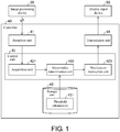
- FIG. 1 is a block diagram illustrating a configuration of main parts of the controller 40.
- the controller 40 includes a reception unit 41, a control unit 42, a storage unit 43, and a transmission unit 44.
- the reception unit 41 receives a signal from an external apparatus.
- the reception unit 41 receives the signal representing the feature value for the jet shape calculated by the image processing device 20 from the image processing device 20.
- the reception unit 41 outputs the received signal to an acquisition unit 421 of the control unit 42.
- the control unit 42 includes a central processing unit (CPU), a random access memory (RAM), a read only memory (ROM), etc., and controls respective configuration elements in response to information processing.
- the control unit 42 includes the acquisition unit 421, an abnormality determination unit 422, and a notification instruction unit 423.
- the acquisition unit 421 acquires the signal indicating the feature value for the imaged jet shape of the solder jet in the jet soldering device 70 from the reception unit 41.
- the abnormality determination unit 422 determines the abnormality of the jet soldering device 70 by using the feature value for the jet shape. Specifically, the abnormality determination unit 422 compares the feature value for the jet shape with a predetermined threshold. In response to the result of the comparison, the abnormality determination unit 422 determines whether the jet soldering device 70 is abnormal. When determining that the jet soldering device 70 is abnormal, the abnormality determination unit 422 outputs a signal indicating the abnormality to the notification instruction unit 423.
- the abnormality determination unit 422 may refer to threshold information 431 indicating the threshold of the feature value (height, width, elliptical major axis, elliptical minor axis, flatness ratio, area, perimeter, circularity, inscribed circle radius, circumscribed circle radius, and gravity center coordinate, etc.) of the jet shape stored in the storage unit 43 and perform the abnormality determination.
- threshold information 431 indicating the threshold of the feature value (height, width, elliptical major axis, elliptical minor axis, flatness ratio, area, perimeter, circularity, inscribed circle radius, circumscribed circle radius, and gravity center coordinate, etc.) of the jet shape stored in the storage unit 43 and perform the abnormality determination.
- the abnormality determination unit 422 may determine the abnormality of the jet soldering device 70 by using at least one of the elliptical major axis, the elliptical minor axis, the flatness ratio, the area, the perimeter, the circularity, the inscribed circle radius, the circumscribed circle radius, and the gravity center coordinate of the jet shape imaged from the top.
- the elliptical major axis, the elliptical minor axis, the flatness ratio, the area, the perimeter, the circularity, the inscribed circle radius, the circumscribed circle radius, and the gravity center coordinate of the jet shape of the solder imaged from the top of the jet soldering device 70 is correlated with the abnormality of the solder jet state. Consequently, according to the above configuration, the abnormality determination with respect to the solder jet state of the jet soldering device 70 can be executed with high detection performance.
- the abnormality determination unit 422 may also determine the abnormality of the jet soldering device 70 by using the width of the jet shape imaged laterally or the position of the vertex of the jet shape in the horizontal direction.
- the width of the jet shape of the solder imaged from a lateral side of the jet soldering device 70 and the position of the vertex of the jet shape in the horizontal direction are correlated with the abnormality of the solder jet state. Consequently, according to the above configuration, the abnormality determination with respect to the solder jet state of the jet soldering device 70 can be executed with high detection performance.
- the abnormality determination unit 422 may perform the determination by using the imaged jet shape when the jet soldering device 70 returns to a home position. Nevertheless, the timing at which the jet shape is imaged is not particularly limited.
- the abnormality determination unit 422 may determine the abnormality of the jet soldering device 70 from one feature value.
- the abnormality determination unit 422 may also determine whether a plurality of feature values are equal to or greater than thresholds, and comprehensively determine the abnormality of the jet soldering device 70 from these determination results. That is, the abnormality determination unit 422 may also determine the abnormality by using multiple types of feature values.
- FIG. 5 illustrates an example of actual values of the elliptical major axes and the elliptical minor axes of the jet shapes imaged from the top in the cases where the solder liquid is jet by using the jet soldering device 70 in the normal solder jet state and the solder liquid is jet by using the jet soldering device 70 in the abnormal solder jet state (the state in which an one-sided flow occurs).
- FIG. 5 is a graph in which the horizontal axis is set as time, the vertical axis is set as the elliptical major axis of the jet shape, and the elliptical major axis of the jet shape of the solder liquid is shown.
- (b) of FIG. 5 is a graph in which the horizontal axis is set as time, the vertical axis is set as the elliptical minor axis of the jet shape, and the elliptical minor axis of the jet shape of the solder liquid is shown.
- FIG. 5 is a graph in which the horizontal axis is set as the elliptical major axis, the vertical axis is set as the elliptical minor axis, and the distributions of the jet shapes in the normal state and the abnormal state are shown.
- the actual values are the elliptical major axes and the elliptical minor axes of the jet shapes calculated by performing an image process on the imaged jet shapes. More specifically, the elliptical major axes and the elliptical minor axes are calculated by processing the jet shapes imaged every 100 ms by an image processing device.
- the horizontal axes of (a) and (b) of FIG. 5 show the number of times the image process is performed. For example, the value "10" shown on the horizontal axis indicates that the image process has been performed for 10 times, and it has been 100 ms * 10, i.e., 1 sec., since the measurement starts.
- the abnormality determination unit 422 performs the following determination.
- the abnormality determination unit 422 determines that the jet soldering device 70 is not abnormal. In addition, in the case where the elliptical major axis or the elliptical minor axis is greater than the predetermined threshold, the abnormality determination unit 422 determines that the jet soldering device 70 is abnormal.
- FIG. 6 illustrates an example of actual values of the flatness ratios of the jet shapes imaged from the top in the cases where the solder liquid is jet by using the jet soldering device 70 in the normal solder jet state and the solder liquid is jet by using the jet soldering device 70 in the abnormal solder jet state (the state in which an one-sided flow occurs).
- FIG. 6 is a graph in which the horizontal axis is set as time, the vertical axis is set as the flatness ratio of the jet shape.
- the flatness ratio is represented as "minor axis M/major axis L".
- the jet shape of the jet soldering device 70 in the normal solder jet state is close to a perfect circle, and the flatness ratio is close to 1.
- the abnormality determination unit 422 performs the following determination. In the case where the flatness ratio of the jet shape is greater than the predetermined threshold, the abnormality determination unit 422 determines that the jet soldering device 70 is not abnormal. In the case where the flatness ratio of the jet shape is equal to or less than the predetermined threshold, the abnormality determination unit 422 determines that the jet soldering device 70 is abnormal.
- FIG. 7 illustrates actual values of the area of the jet shapes imaged from the top in the cases where the solder liquid is jet by using the jet soldering device 70 in the normal solder jet state and the solder liquid is jet by using the jet soldering device 70 in the abnormal solder jet state (the state in which an one-sided flow occurs).
- FIG. 7 is a graph in which the horizontal axis is set as time, the vertical axis is set as the area of the jet shape.
- the abnormality determination unit 422 performs the following determination. In the case where the area of the jet shape is within the predetermined threshold, the abnormality determination unit 422 determines that the jet soldering device 70 is not abnormal. In the case where the area of the jet shape is greater than the predetermined threshold, the abnormality determination unit 422 determines that the jet soldering device 70 is abnormal.
- FIG. 8 illustrates actual values of the perimeter of the jet shapes imaged from the top in the cases where the solder liquid is jet by using the jet soldering device 70 in the normal solder jet state and the solder liquid is jet by using the jet soldering device 70 in the abnormal solder jet state (the state in which an one-sided flow occurs).
- FIG. 8 is a graph in which the horizontal axis is set as time, the vertical axis is set as the perimeter (length of the periphery) of the jet shape.
- the abnormality determination unit 422 performs the following determination. In the case where the perimeter of the jet shape is within the predetermined threshold, the abnormality determination unit 422 determines that the jet soldering device 70 is not abnormal. In the case where the perimeter of the jet shape is greater than the predetermined threshold, the abnormality determination unit 422 determines that the jet soldering device 70 is abnormal.
- FIG. 9 illustrates actual values of the circularity of the jet shapes imaged from the top in the cases where the solder liquid is jet by using the jet soldering device 70 in the normal solder jet state and the solder liquid is jet by using the jet soldering device 70 in the abnormal solder jet state (the state in which an one-sided flow occurs).
- FIG. 9 is a graph in which the horizontal axis is set as time, the vertical axis is set as circularity.
- the abnormality determination unit 422 performs the following determination. In the case where the circularity of the jet shape is equal to or greater than the predetermined threshold, the abnormality determination unit 422 determines that the jet soldering device 70 is not abnormal. In the case where the perimeter of the jet shape is less than the predetermined threshold, the abnormality determination unit 422 determines that the jet soldering device 70 is abnormal.
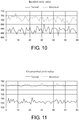
- FIG. 10 illustrates actual values of the inscribed circle radius of the jet shapes imaged from the top in the cases where the solder liquid is jet by using the jet soldering device 70 in the normal solder jet state and the solder liquid is jet by using the jet soldering device 70 in the abnormal solder jet state (the state in which an one-sided flow occurs).
- FIG. 10 is a graph in which the horizontal axis is set as time, the vertical axis is set as the inscribed circle radius of the jet shape.
- the abnormality determination unit 422 performs the following determination. In the case where the inscribed circle radius of the jet shape is within the predetermined threshold, the abnormality determination unit 422 determines that the jet soldering device 70 is not abnormal. In the case where the inscribed circle radius is greater than the predetermined threshold, the abnormality determination unit 422 determines that the jet soldering device 70 is abnormal.
- FIG. 11 illustrates actual values of the circumscribed circle radius of the jet shapes imaged from the top in the cases where the solder liquid is jet by using the jet soldering device 70 in the normal solder jet state and the solder liquid is jet by using the jet soldering device 70 in the abnormal solder jet state (the state in which an one-sided flow occurs).
- FIG. 11 is a graph in which the horizontal axis is set as time, the vertical axis is set as the circumscribed circle radius of the jet shape.
- the abnormality determination unit 422 performs the following determination. In the case where the circumscribed circle radius of the jet shape is within the predetermined threshold, the abnormality determination unit 422 determines that the jet soldering device 70 is not abnormal. In the case where the circumscribed circle radius is greater than the predetermined threshold, the abnormality determination unit 422 determines that the jet soldering device 70 is abnormal.
- FIG. 12 illustrates actual values of the width of the jet shapes imaged laterally in the cases where the solder liquid is jet by using the jet soldering device 70 in the normal solder jet state and the solder liquid is jet by using the jet soldering device 70 in the abnormal solder jet state (the state in which an one-sided flow occurs).
- FIG. 12 is a graph in which the horizontal axis is set as time, the vertical axis is set as the width of the jet shape.
- the abnormality determination unit 422 performs the following determination. In the case where the width of the jet shape is within the predetermined threshold, the abnormality determination unit 422 determines that the jet soldering device 70 is not abnormal. In the case where the width of the jet shape is greater than the predetermined threshold, the abnormality determination unit 422 determines that the jet soldering device 70 is abnormal.
- the actual value of the height of the jet shape imaged laterally is greater in the case where the solder liquid is jet in the normal solder jet state than in the case where the solder liquid is jet in the abnormal solder jet state. That is, in the case where the height of the jet shape is equal to or greater than the predetermined threshold, the abnormality determination unit 422 may determine that the jet soldering device 70 is not abnormal. In the case where the height of the jet shape is less than the predetermined threshold, the abnormality determination unit 422 may determine that the jet soldering device 70 is abnormal.
- the direction in which the solder liquid is jet (upper direction) is set as the Z-axis direction
- an arbitrary direction perpendicular to the Z-axis direction is set as the X-axis direction
- an arbitrary direction perpendicular to the Z-axis direction and the X-axis direction is set as the Y-axis direction.
- FIG. 13 is a schematic view in which the horizontal axis is set as the X-axis and the vertical axis is set as the Y-axis, and which illustrates the gravity center coordinates of the jet shapes and the jet shapes imaged from the top in the cases where the solder liquid is jet by using the jet soldering device 70 in the normal solder jet state and the solder liquid is jet by using the jet soldering device 70 in the abnormal solder jet state (the state in which an one-sided flow occurs).
- a of FIG. 13 shows the jet shape in the normal solder jet state, and Ga shows the gravity center coordinate of the jet shape in the normal solder jet state.
- B of FIG. 13 shows the jet shape in the abnormal solder jet state, and Gb shows the gravity center coordinate of the jet shape in the abnormal solder jet state.
- Gc of FIG. 13 shows a reference point.
- the abnormality determination unit 422 performs the following determination. Firstly, the reference point is set in advance in the storage unit 43 as a preferred position for the gravity center coordinate of the jet shape in the normal solder jet state to exist.
- the abnormality determination unit 422 determines that the jet soldering device 70 is not abnormal. Also, in the case where the distance from the reference point to the gravity center coordinate of the jet shape is greater than the predetermined threshold, the abnormality determination unit 422 determines that the jet soldering device 70 is abnormal.
- FIG. 14 is a schematic view in which the horizontal axis is set as the X-axis and the vertical axis is set as the Z-axis, and which illustrates the vertex coordinates of the jet shapes and the jet shapes laterally imaged in the cases where the solder liquid is jet by using the jet soldering device 70 in the normal solder jet state and the solder liquid is jet by using the jet soldering device 70 in the abnormal solder jet state (the state in which an one-sided flow occurs).
- a of FIG. 14 shows the jet shape in the normal solder jet state
- Ga shows the vertex coordinate of the jet shape in the normal solder jet state.
- B of FIG. 14 shows the jet shape in the case where a nozzle in the abnormal solder jet state is used
- Gb shows the vertex coordinate of the jet shape in the abnormal solder jet state.
- Gc of FIG. 14 shows a reference point.
- the abnormality determination unit 422 performs the following determination. Firstly, the reference point is set in advance in the storage unit 43 as a preferred position for the vertex of the jet shape in the horizontal direction under the normal solder jet state to exist.
- the abnormality determination unit 422 determines the abnormality of the jet soldering device 70 based on the distance from the reference point to the X-axis coordinate of the vertex of the jet shape and the distance from the reference point to the Z-axis coordinate of the vertex of the jet shape. Specifically, in the case where the distance from the reference point to the X-axis coordinate of the vertex of the jet shape is equal to or less than the predetermined threshold (referred to as "first threshold"), and in the case where the distance from the reference point to the Z-axis coordinate of the vertex of the jet shape is equal to or less than the predetermined threshold (referred to as "second threshold"), the abnormality determination unit 422 determines that the jet soldering device 70 is not abnormal.
- the abnormality determination unit 422 determines that the jet soldering device 70 is abnormal.
- the abnormality determination unit 422 may also determine the abnormality of the jet soldering device 70 based on only the X-axis coordinate of the vertex of the jet shape from the reference point. Specifically, in the case where the distance from the reference point to the X-axis coordinate of the vertex of the jet shape is equal to or less than the predetermined threshold, the abnormality determination unit 422 determines that the jet soldering device 70 is not abnormal. In the case where the distance from the reference point to the X-axis coordinate of the vertex of the jet shape exceeds the predetermined threshold, the abnormality determination unit 422 determines that the jet soldering device 70 is abnormal.
- the abnormality determination unit 422 determines that the jet soldering device 70 is not abnormal. In the case where the distance from the reference point to the vertex of the jet shape in the horizontal direction is greater than the predetermined threshold, the abnormality determination unit 422 determines that the jet soldering device 70 is abnormal. In the case where there are a plurality of cameras 10b, for the respective jet shapes imaged by the cameras 10b, the abnormality determination unit 42 may obtain the distances from the respective reference points to the respective vertices in the horizontal direction (X-axis direction or Y-axis direction) and make determinations respectively.
- the height of the vertex of the jet shape is influenced by the jet velocity of the solder liquid. Meanwhile, the position of the vertex of the jet shape in the horizontal direction is hardly influenced by the jet velocity of the solder liquid.
- the abnormality determination unit 422 can suitably determine the abnormality of the jet soldering device 70.
- the notification instruction unit 423 receives the signal indicating the abnormality output by the abnormality determination unit 422, and outputs a signal instructing to notify a sign of abnormality to the display input device 50 via the transmission unit 44. Specifically, the notification instruction unit 423 in the embodiment may output a signal instructing to notify a sign of abnormality of the jet state of the solder jet from the nozzle 77.
- the storage unit 43 is, for example, an auxiliary storage device such as a flash memory, a solid state drive, etc., and stores the threshold information 431.
- the transmission unit 44 outputs a signal to the external apparatus.
- the transmission unit 44 follows the instruction of the notification instruction unit 423 and output the signal indicating that the jet soldering device 70 is abnormal to the display input device 50.
- the display input device 50 is, for example, a touch panel-type display input device.
- the user of the management system 1 can operate the controller 40 via the display input device 50 and check the operation state of the management system 1 on the display input device 50.
- the display input device 50 receives the signal indicating the instruction to notify that the jet soldering device 70 has a sign of abnormality and performs the notification indicating the sign of abnormality.
- the notification relating to the abnormality may be displayed on a touch panel included in the display input device 50.
- the support device 60 is a device used by connecting with the management system 1 for various settings in the management system 1, such as the operation settings of the camera 10a, the camera 10b, the image processing device 20, and the jet soldering device 70.
- the support device 60 can be connected with the management system 1 via the controller 40.
- An information processing device such as a personal computer, can be used as the support device 60, or a portable information processing device, such as a notebook computer, can also be used as the support device 60.
- FIG. 15 is a flowchart illustrating an example of a flow of an abnormality notification process of the management system 1. An example of the flow of the abnormality notification process of the management system 1 is described with reference to FIG. 15 .
- the abnormality determination unit 422 performs abnormality determination by using a feature value whose value is smaller in the case where the solder liquid is jet in the normal solder jet state than the case where the solder liquid is jet in the abnormal solder jet state.
- the camera 10a and the camera 10b image the jet shape of the jet solder (S21).
- the image processing device 20 performs an image process that calculates the feature value representing the height, the width, the elliptical major axis, the elliptical minor axis, the flatness ratio, the area, the perimeter, the circularity, the inscribed circle radius, the circumscribed circle radius, and the gravity center coordinate, etc., of the jet shape of the solder from the image data output by the camera 10a and the camera 10b (S22).
- the acquisition unit 421 acquires the feature value calculated by the image processing device 20.
- the abnormality determination unit 422 determines whether the feature value for the jet shape is within the predetermined threshold (S24: Abnormality Determination Step).
- the display input device 50 notifies with a sign of abnormality regarding the abnormality of the jet state of the solder jet from the nozzle 77 (S25). In addition, in the case where the feature value is within the predetermined threshold (YES in S24), the process is ended.
- a configuration in which the abnormality determination unit 422 performs abnormality determination by using a feature value whose value is greater in the case where the solder liquid is jet in the normal solder jet state than the case where the solder liquid is jet in the abnormal solder jet state is as follows.
- the display input device 50 notifies with a sign of abnormality regarding the abnormality of the jet state of the solder jet from the nozzle 77.
- the process is ended.
- the abnormality determination unit 422 may also perform abnormality determination based on multiple types of feature values. For example, the abnormality determination unit 422 may perform determination based on another feature value in response to a result of performing determination based on a first feature value. The abnormality determination unit 422 may, in response to the result of performing the determination based on the first feature value, make a feature value used as the another feature value different.
- the abnormality determination unit 422 may further perform abnormality determination based on a second feature value.
- the abnormality determination unit 422 may further perform abnormality determination based on a third feature value.
- the abnormality determination unit 422 may, in response to a result of determination of the second time (the result of the determination according to the second feature value or the third feature value), determine whether jet soldering device 70 is abnormal.
- the control program (specifically the acquisition unit 421, the abnormality determination unit 422, and the notification instruction unit 423) of the controller 40 may be realized as a logic circuit (hardware) formed by an integrated circuit (IC chip), etc., and may also be realized by software.
- the controller 40 includes a computer that executes the commands of the program which is the software that realizes the respective functions.
- the computer includes, for example, one or more processors as well as a computer readable recording medium storing the program. Then, in the computer, the processor reads the program from the recording medium and executes the program, thereby achieving the objective of the invention.
- a central processing unit CPU
- the recording medium in addition to a "non-temporary tangible medium" such as a read only memory (ROM), etc., a tape, a disk, a card, a semiconductor memory, a programmable logic circuit, or the like can be used. Further, a random access memory (RAM) for expanding the program may be further provided.
- ROM read only memory
- RAM random access memory
- the program may be supplied to the computer via an arbitrary transmission medium (communication network, broadcast wave, etc.) capable of transmitting the program.
- an aspect of the invention may be realized in the form of data signals embedded in carrier waves, in which the program is embodied through electronic transmission.
- the abnormality determination of the jet soldering device 70 is performed based on multiple types of feature values by using the management system 1.
- the abnormality determination unit 422 determines that the state is a normal state in the case where the flatness ratio exceeds 0.9, and determines that the state is an abnormal state in the case where the flatness ratio is equal to or less than 0.9.
- the jet soldering device 70 is determined as in the normal state in 70 cases, and the jet soldering device 70 is determined as in the abnormal state in 30 cases.
- the determination is performed on the X-axis coordinates of the gravity center coordinates of the jet shapes of the jet soldering device 70 in the 70 cases determined as in the normal state based on the flatness ratio (Determination 2).
- the abnormality determination unit 422 determines that the state is a normal state in the case where the X-axis coordinate of the gravity center coordinate is less than 2, and determines that the state is an abnormal state in the case where the X-axis coordinate of the gravity center coordinate exceeds 2.
- the jet soldering device 60 is determined as in the normal state in 70 cases, and the jet soldering device 70 is determined as in the abnormal state in 10 cases.
- the determination is performed on the X-axis coordinates of the vertex coordinates of the jet shapes of the jet soldering device 70 in the 30 cases determined as in the abnormal state based on the flatness ratio (Determination 3).
- the abnormality determination unit 422 determines that the state is a normal state in the case where the X-axis coordinate of the vertex coordinate is less than 3, and determines that the state is an abnormal state in the case where the X-axis coordinate of the vertex coordinate exceeds 3.
- the jet soldering device 10 is determined as in the normal state in 70 cases, and the jet soldering device 70 is determined as in the abnormal state in 20 cases.
- the 100 cases of the jet soldering device 70 there are 70 cases that are actually in the normal state and 30 cases that are actually in the abnormal state.
- the 70 cases determined as in the normal state in Determination 1 there are 60 cases that are actually in the normal state and 10 cases that are actually in the abnormal state.
- the data of 10 cases that are actually in the abnormal state are overlooked.
- the 70 cases determined as in the abnormal state in Determination 1 there are 20 cases that are actually in the abnormal state and 10 cases that are actually in the normal state.
- the data of 10 cases that are actually in the normal state are determined as in the abnormal state. From the above, in the case where the determination on 100 cases is performed based on only one type of feature values (flatness ratio), there are 20 cases that are determined erroneously, and the identification success rate is 80%.
- the 60 cases determined as in the normal state in Determination 2 there are 60 cases that are actually in the normal state and 0 cases that are actually in the abnormal state.
- the 10 cases determined as in the abnormal state in Determination 1 there are 10 cases that are actually in the abnormal state and 0 cases that are actually in the normal state. That is, in the case where the determination is performed based on two types of feature values, there are 0 cases that are determined erroneously, and the identification success rate is 100%.
- the identification success rate is increased. That is, by performing abnormality determination based on multiple types of feature values, the determination accuracy can be even higher than the abnormality determination based on one type of feature values.
Landscapes
- Engineering & Computer Science (AREA)
- Mechanical Engineering (AREA)
- Quality & Reliability (AREA)
- Manufacturing & Machinery (AREA)
- Microelectronics & Electronic Packaging (AREA)
- Computer Vision & Pattern Recognition (AREA)
- Physics & Mathematics (AREA)
- General Physics & Mathematics (AREA)
- Theoretical Computer Science (AREA)
- Electric Connection Of Electric Components To Printed Circuits (AREA)
- Molten Solder (AREA)
Abstract
Description
- The invention relates to an information processing device, a management system, a control program, and a control method for an information processing device for determining abnormalities in a jet soldering device.
- Techniques are known for adjusting solder jet in a jet soldering device. For example,
Patent Documents 1 to 3 disclose techniques for detecting the height of the solder that is jet, adjusting the height of the solder that is jet, etc. -
- Patent Document 1: Japanese Laid-open No.
H11-047922 - Patent Document 2: Japanese Laid-open No.
H05-185209 - Patent Document 3: Japanese Laid-open No.
H01-205593 - In the conventional technologies as described above, the height of the solder is adjusted according to the temporary height of the solder. Therefore, when a device that performs abnormality determination with respect to a jet soldering device is to be realized by using these technologies, the abnormality determination is performed by using the height of the jet solder.
- However, when an abnormality occurs in the jet soldering device, features of the jet shape of the solder other than height may also change. Therefore, in the case where the abnormalities are determined by using only the height of the solder, it is possible that the abnormalities cannot be detected correctly.
- An objective of an aspect of the invention is to realize an information processing device, etc., capable of determining, with high detection performance, abnormalities in jet soldering devices.
- In order to solve the above issues, an aspect of the invention provides an information processing device. The information processing device includes: an acquisition unit, acquiring a feature value for an imaged jet shape of solder jet in a jet soldering device; and an abnormality determination unit, determining an abnormality of the jet soldering device by using the feature value.
- In addition, an aspect of the invention provides a control method for an information processing device. The control method includes: an acquisition step for acquiring a feature value for an imaged jet shape of solder jet in a jet soldering device; and an abnormality determination step for determining an abnormality of the jet soldering device by using the feature value.
- The jet shape of the solder of the jet soldering device is correlated with the abnormality of the jet soldering device. For example, as the jet shape, a feature value other than height can also be used. Therefore, in the configuration in which the state of the jet soldering device is determined from the jet shape of the solder, the abnormality in the jet soldering device can be determined with high detection performance.
- Accordingly, the user can recognize the quality deterioration tendency of the solder from the determination and the effect of being capable of avoiding soldering defects of the jet soldering device in advance is achieved.
- The abnormality determination unit may determine the abnormality of the jet soldering device by using the feature value of the jet shape that is imaged from top.
- In the jet soldering device, the abnormality of the solder jet state influences the jet shape imaged from the top. Therefore, according to the configuration, for example, the effect of being capable of determining the abnormality of the jet state of the solder jet from the jet soldering device from the feature value for the jet shape of the solder imaged from the top is achieved.
- The abnormality determination unit may determine the abnormality of the jet soldering device by using, as the feature value, at least one of an elliptical major axis, an elliptical minor axis, a flatness ratio, an area, a perimeter, circularity, an inscribed circle radius, a circumscribed circle radius, and a gravity center coordinate of the jet shape imaged from the top.
- The elliptical major axis, the elliptical minor axis, the flatness ratio, the area, the perimeter, the circularity, the inscribed circle radius, the circumscribed circle radius, and the gravity center coordinate of the jet shape of the solder imaged from the top of the jet soldering device is correlated with the abnormality of the solder jet state.
- Thus, according to the above configuration, by using at least one of the elliptical major axis, the elliptical minor axis, the flatness ratio, the area, the perimeter, the circularity, the inscribed circle radius, the circumscribed circle radius, and the gravity center coordinate of the jet shape imaged from the top, the effect of being capable of determining the abnormality with respect to the solder jet state of the jet soldering device with high detection performance is achieved.
- The abnormality determination unit may determine the abnormality of the jet soldering device by using the feature value of the jet shape that is imaged laterally.
- In the jet soldering device, the abnormality of the solder jet state influences the jet shape imaged laterally. Therefore, according to the configuration, for example, the effect of being capable of determining the abnormality of the jet state of the solder jet from the jet soldering device from the feature value for the jet shape of the solder is achieved.
- The abnormality determination unit may determine the abnormality of the jet soldering device by using, as the feature value, a width of the jet shape imaged laterally or a position of a vertex of the jet shape in a horizontal direction.
- The width of the jet shape of the solder imaged from a lateral side of the jet soldering device and the position of the vertex of the jet shape in the horizontal direction are correlated with the abnormality of the solder jet state.
- Thus, according to the above configuration, by using the width of the jet shape imaged laterally or the position of the vertex of the jet shape in the horizontal direction, the effect of being capable of determining the abnormality with respect to the solder jet state of the jet soldering device with high detection performance is achieved.
- In order to solve the above issues, an aspect of the invention provides a management system. The management system includes: a camera, imaging a jet shape of a solder liquid jet in a jet soldering device; an image processing device, calculating a feature value for the jet shape from an image imaged by the camera; and any of the above information processing device.
- According to the above configuration, the effect of being capable of realizing an abnormality determination system capable of determining the abnormality of the jet soldering device is achieved.
- In order to solve the above issues, an aspect of the invention provides a control program. The control program is a control program for a computer to function as the information processing device, and the computer functions as the acquisition unit and the abnormality determination unit.
- According to an aspect of the invention, the abnormalities in the jet soldering device can be determined with high detection performance.
-
-
FIG. 1 is a block diagram illustrating a configuration of main parts of a controller according to an embodiment of the invention. -
FIG. 2 is a diagram illustrating an example of an application example of a controller in a management system according to an embodiment of the invention. - In
FIG. 3 , (a) to (e) are views illustrating jet shapes in cases where a solder liquid is jet by using a jet soldering device in a normal solder jet state and a solder liquid is jet by using a jet soldering device in an abnormal solder jet state. -
FIG. 4 is a view illustrating a cross-section of a jet soldering device according to an embodiment of the invention. - In
FIG. 5 , (a) to (c) are diagrams illustrating actual values of elliptical major axes and elliptical minor axes of jet shapes imaged from the top in cases where a solder liquid is jet by using a jet soldering device in a normal solder jet state and a solder liquid is jet by using a jet soldering device in an abnormal solder jet state. -
FIG. 6 is a diagram illustrating actual values of flatness ratios of jet shapes imaged from the top in cases where a solder liquid is jet by using a jet soldering device in a normal solder jet state and a solder liquid is jet by using a jet soldering device in an abnormal solder jet state. -
FIG. 7 is a diagram illustrating actual values of areas of jet shapes imaged from the top in cases where a solder liquid is jet by using a jet soldering device in a normal solder jet state and a solder liquid is jet by using a jet soldering device in an abnormal solder jet state. -
FIG. 8 is a diagram illustrating actual values of perimeters of jet shapes imaged from the top in cases where a solder liquid is jet by using a jet soldering device in a normal solder jet state and a solder liquid is jet by using a jet soldering device in an abnormal solder jet state. -
FIG. 9 is a diagram illustrating actual values of circularity of jet shapes imaged from the top in cases where a solder liquid is jet by using a jet soldering device in a normal solder jet state and a solder liquid is jet by using a jet soldering device in an abnormal solder jet state. -
FIG. 10 is a diagram illustrating actual values of inscribed circle radii of jet shapes imaged from the top in cases where a solder liquid is jet by using a jet soldering device in a normal solder jet state and a solder liquid is jet by using a jet soldering device in an abnormal solder jet state. -
FIG. 11 is a diagram illustrating actual values of circumscribed circle radii of jet shapes imaged from the top in cases where a solder liquid is jet by using a jet soldering device in a normal solder jet state and a solder liquid is jet by using a jet soldering device in an abnormal solder jet state. -
FIG. 12 is a diagram illustrating actual values of widths of jet shapes imaged laterally in cases where a solder liquid is jet by using a jet soldering device in a normal solder jet state and a solder liquid is jet by using a jet soldering device in an abnormal solder jet state. -
FIG. 13 is a view illustrating gravity center coordinates of jet shapes imaged from the top in cases where a solder liquid is jet by using a jet soldering device in a normal solder jet state and a solder liquid is jet by using a jet soldering device in an abnormal solder jet state. -
FIG. 14 is a view illustrating vertex coordinates of jet shapes imaged laterally in cases where a solder liquid is jet by using a jet soldering device in a normal solder jet state and a solder liquid is jet by using a jet soldering device in an abnormal solder jet state. -
FIG. 15 is a flowchart illustrating an example of a flow of an abnormality notification process of a management system according to an embodiment of the invention. - In the following, an embodiment of the invention will be described in detail.
-
FIG. 2 is a diagram illustrating an example of an application example of a controller (information processing device) 40 in amanagement system 1. Firstly, the outline of an application example of thecontroller 40 is described by usingFIG. 2 . - In a
jet soldering device 70, for example, when the solder deteriorates due to oxidation, etc., oxide debris of the solder adheres to the inner surface of a nozzle for jetting the solder and clogs the nozzle. In addition, in thejet soldering device 70, the tip of the nozzle may be worn out due to use for a long time, which makes the jet flow not uniform and causes a one-sided flow in which the solder flow is deviated toward a direction. In addition, when the temperature of the solder stored in thejet soldering device 70 decreases, the solder is jet in a cured state and causes an abnormality of the jet shape of the solder. These abnormalities of the solder jet states cause an insufficient solder amount during soldering, a soldering defect such as a bridge due to the solder, etc., and lower the product yield. - The
management system 1 is a system which determines the abnormalities of thejet soldering device 70. Themanagement system 1 includes acamera 10a, acamera 10b, acontroller 40, thejet soldering device 70, etc. The detailed configuration of themanagement system 1 will be described in the following. - The
controller 40 acquires a feature value for an imaged jet shape of the solder jet in thejet soldering device 70. Here, the feature value for the jet shape is a numerical data indicating a jet shape. In addition, thecontroller 40 determines whether thejet soldering device 70 is abnormal by using the feature value. -
FIG. 3 illustrates the jet shapes in the cases where a solder liquid is jet by using thejet soldering device 70 in a normal solder jet state and the solder liquid is jet by using thejet soldering device 70 in an abnormal solder jet state (a state in which a one-sided flow occurs). (a) and (b) ofFIG. 3 are binarized images of jet shapes in the case where the solder liquid is jet in the normal solder jet state. (a) ofFIG. 3 is an image imaged from the top of the jet shape. (b) ofFIG. 3 is an image imaged from a lateral side of the jet shape. (c) and (d) ofFIG. 3 are binarized images of jet shapes in the case where the solder liquid is jet in the abnormal solder jet state. (c) ofFIG. 3 is an image imaged from the top of the jet shape. (d) ofFIG. 3 is an image imaged from a lateral side of the jet shape. In (b) and (d) ofFIG. 3 , the jet direction of the solder liquid is reversed from the actual jet direction. In these figures, the solder liquid is jet toward the lower side. (e) ofFIG. 3 is a schematic view illustrating a change of the jet shape of the solder liquid when is viewed from the top, in a case where the solder jet state changes from normal to abnormal. - As shown in
FIG. 3 , in thejet soldering device 70, the abnormalities of the solder jet state influence the height, the width, the elliptical major axis, the elliptical minor axis, the flatness ratio, the area, the perimeter, the circularity, the inscribed circle radius, the circumscribed circle radius, and the gravity center coordinate, etc., of the jet shape of the solder imaged from a fixed position. - Specifically, with the solder flow being deviated toward a direction, a one-sided solder flow occurs. Therefore, as the abnormalities of the solder jet state progress, the jet shape, when viewed from the top, may change from a circular shape to an elliptical shape.
- Therefore, for example, an abnormality of the jet state of the solder jet from the
jet soldering device 70 can be determined from at least one feature value among the height, the width, the elliptical major axis, the elliptical minor axis, the flatness ratio, the area, the perimeter, the circularity, the inscribed circle radius, the circumscribed circle radius, and the gravity center coordinate, etc., of the jet shape of the solder. - If an element other than the height, the width, the elliptical major axis, the elliptical minor axis, the flatness ratio, the area, the perimeter, the circularity, the inscribed circle radius, the circumscribed circle radius, and the gravity center coordinate, etc., of the jet shape of the solder is an element of the jet shape influenced by the abnormalities of the solder jet state, such an element can also be applied in the abnormality determination.
- As described above, the jet shape (height as well as feature values other than height) of the solder of the
jet soldering device 70 is correlated with the abnormalities of thejet soldering device 70. For example, as the jet shape, a feature value other than height can also be used. Therefore, in the configuration in which the state of thejet soldering device 70 is determined from the jet shape that is imaged, the abnormalities in thejet soldering device 70 can be determined with high detection performance. - Accordingly, the user can recognize the quality deterioration tendency of the solder from the determination and the effect of being capable of avoiding soldering defects of the jet soldering device in advance is achieved.
- Then, an example of the
management system 1 according to the embodiment will be described. - As shown in
FIG. 2 , themanagement system 1 includes thecamera 10a, thecamera 10b, animage processing device 20, acommunication coupler 30, thecontroller 40, adisplay input device 50, asupport device 60, and thejet soldering device 70. -
FIG. 4 is a view illustrating a cross-section of thejet soldering device 70 according to the embodiment. Thejet soldering device 70 jets a dissolved solder liquid, and performs soldering on a substrate, etc. As shown inFIG. 4 , thejet soldering device 70 includes amotor 71, atransmission 72, apump 73, a thermocouple 74, aheater 75, asolder tank 76, and anozzle 77. - The
jet soldering device 70 makes the dissolved solder liquid flow into thenozzle 77 by using a pressure generated by thepump 73 and jets the solder liquid from thenozzle 77. InFIG. 4 , a height h is the height from the end of thenozzle 77 to a liquid surface p of the jet solder liquid. - In addition, as shown in
FIG. 4 , thepump 73 includes themotor 71 and thetransmission 72. For example, thecontroller 40 may also control the rotation speed of themotor 71, thetransmission 72, etc., via a network and control the height of the jet flow of the solder liquid. - In addition, the thermocouple 74 detects the temperature of the solder stored in the
solder tank 76. For example, a signal indicating the detection value detected by the thermocouple 74 may be output to thecontroller 40 via the network. Thecontroller 40 may refer to the detected value detected by the thermocouple 74 and control theheater 75 via the network, and manage the temperature of the solder stored in thesolder tank 76. - The
camera 10a and thecamera 10b image the jet shape of the solder liquid jet in thejet soldering device 70 from fixed positions. For example, thecamera 10a images the jet shape from the top, and thecamera 10b laterally images the jet shape. - It is not required to dispose the
camera 10a right on the top the jet solder liquid. Thecamera 10a may be disposed within a predetermined range from the top of the jet solder liquid. That is, thecamera 10a may also image the jet shape from an obliquely upper side. Thecamera 10a and thecamera 10b output the imaged image data to theimage processing device 20. For example, thecamera 10a and thecamera 10b may image the jet shape at an interval of 100 ms. While the embodiment is described with the configuration of themanagement system 1 including two cameras, i.e., thecamera 10a and thecamera 10b, it suffices as long as the management system includes at least one camera. - The
image processing device 20 calculates the feature value (numerical data) of the height, the width, the elliptical major axis, the elliptical minor axis, the flatness ratio, the area, the perimeter, the circularity, the inscribed circle radius, the circumscribed circle radius, and the gravity center coordinate, etc., of the jet shape of the solder from the image data output from thecamera 10a and thecamera 10b. Theimage processing device 20 outputs a signal indicating the calculated feature value to thecontroller 40 via thecommunication coupler 30. Theimage processing device 20 may calculate each feature value after binarizing the image data output from thecamera 10a and thecamera 10b, and may also directly calculate each feature value from the image data output from thecamera 10a and thecamera 10b. - The
communication coupler 30 is a relay device which relays the communication between a superordinate network and theimage processing device 20. Thecommunication coupler 30 relays the communication between an apparatus including the superordinate network and theimage processing device 20. - The
controller 40 is a control device that controls theentire management system 1, and may use a programmable logic controller (PLC). Thecontroller 40 operates as a master device of thecommunication coupler 30 and thejet soldering device 70 in themanagement system 1. In addition, in the embodiment, thecontroller 40 determines the abnormality of thejet soldering device 70. Thecontroller 40 can be replaced with a control program executed by a data server, a client server, etc. -
FIG. 1 is a block diagram illustrating a configuration of main parts of thecontroller 40. As shown inFIG. 1 , thecontroller 40 includes areception unit 41, acontrol unit 42, astorage unit 43, and atransmission unit 44. - The
reception unit 41 receives a signal from an external apparatus. In the embodiment, specifically, thereception unit 41 receives the signal representing the feature value for the jet shape calculated by theimage processing device 20 from theimage processing device 20. Thereception unit 41 outputs the received signal to anacquisition unit 421 of thecontrol unit 42. - The
control unit 42 includes a central processing unit (CPU), a random access memory (RAM), a read only memory (ROM), etc., and controls respective configuration elements in response to information processing. Thecontrol unit 42 includes theacquisition unit 421, anabnormality determination unit 422, and anotification instruction unit 423. - The
acquisition unit 421 acquires the signal indicating the feature value for the imaged jet shape of the solder jet in thejet soldering device 70 from thereception unit 41. - The
abnormality determination unit 422 determines the abnormality of thejet soldering device 70 by using the feature value for the jet shape. Specifically, theabnormality determination unit 422 compares the feature value for the jet shape with a predetermined threshold. In response to the result of the comparison, theabnormality determination unit 422 determines whether thejet soldering device 70 is abnormal. When determining that thejet soldering device 70 is abnormal, theabnormality determination unit 422 outputs a signal indicating the abnormality to thenotification instruction unit 423. Theabnormality determination unit 422 may refer tothreshold information 431 indicating the threshold of the feature value (height, width, elliptical major axis, elliptical minor axis, flatness ratio, area, perimeter, circularity, inscribed circle radius, circumscribed circle radius, and gravity center coordinate, etc.) of the jet shape stored in thestorage unit 43 and perform the abnormality determination. - For example, the
abnormality determination unit 422 may determine the abnormality of thejet soldering device 70 by using at least one of the elliptical major axis, the elliptical minor axis, the flatness ratio, the area, the perimeter, the circularity, the inscribed circle radius, the circumscribed circle radius, and the gravity center coordinate of the jet shape imaged from the top. - The elliptical major axis, the elliptical minor axis, the flatness ratio, the area, the perimeter, the circularity, the inscribed circle radius, the circumscribed circle radius, and the gravity center coordinate of the jet shape of the solder imaged from the top of the
jet soldering device 70 is correlated with the abnormality of the solder jet state. Consequently, according to the above configuration, the abnormality determination with respect to the solder jet state of thejet soldering device 70 can be executed with high detection performance. - In addition, the
abnormality determination unit 422 may also determine the abnormality of thejet soldering device 70 by using the width of the jet shape imaged laterally or the position of the vertex of the jet shape in the horizontal direction. - The width of the jet shape of the solder imaged from a lateral side of the
jet soldering device 70 and the position of the vertex of the jet shape in the horizontal direction are correlated with the abnormality of the solder jet state. Consequently, according to the above configuration, the abnormality determination with respect to the solder jet state of thejet soldering device 70 can be executed with high detection performance. - For example, the
abnormality determination unit 422 may perform the determination by using the imaged jet shape when thejet soldering device 70 returns to a home position. Nevertheless, the timing at which the jet shape is imaged is not particularly limited. - In addition, the
abnormality determination unit 422 may determine the abnormality of thejet soldering device 70 from one feature value. Theabnormality determination unit 422 may also determine whether a plurality of feature values are equal to or greater than thresholds, and comprehensively determine the abnormality of thejet soldering device 70 from these determination results. That is, theabnormality determination unit 422 may also determine the abnormality by using multiple types of feature values. - In the following, the feature values for the jet shapes in the normal solder jet state and the abnormal solder jet state are described in detail.
-
FIG. 5 illustrates an example of actual values of the elliptical major axes and the elliptical minor axes of the jet shapes imaged from the top in the cases where the solder liquid is jet by using thejet soldering device 70 in the normal solder jet state and the solder liquid is jet by using thejet soldering device 70 in the abnormal solder jet state (the state in which an one-sided flow occurs). - (a) of
FIG. 5 is a graph in which the horizontal axis is set as time, the vertical axis is set as the elliptical major axis of the jet shape, and the elliptical major axis of the jet shape of the solder liquid is shown. (b) ofFIG. 5 is a graph in which the horizontal axis is set as time, the vertical axis is set as the elliptical minor axis of the jet shape, and the elliptical minor axis of the jet shape of the solder liquid is shown. (c) ofFIG. 5 is a graph in which the horizontal axis is set as the elliptical major axis, the vertical axis is set as the elliptical minor axis, and the distributions of the jet shapes in the normal state and the abnormal state are shown. - The actual values are the elliptical major axes and the elliptical minor axes of the jet shapes calculated by performing an image process on the imaged jet shapes. More specifically, the elliptical major axes and the elliptical minor axes are calculated by processing the jet shapes imaged every 100 ms by an image processing device. The horizontal axes of (a) and (b) of
FIG. 5 show the number of times the image process is performed. For example, the value "10" shown on the horizontal axis indicates that the image process has been performed for 10 times, and it has been 100 ms * 10, i.e., 1 sec., since the measurement starts. In addition, the horizontal axes of (a) and (b) ofFIG. 5 show the value of the elliptical major axis or the elliptical minor axis. Also, the values of the elliptical major axis or the elliptical minor axis shown in (a) to (c) ofFIG. 5 are values used for convenience, and are not conventionally defined physical quantities. - The values of the horizontal axes (time) and the values (actual values) of the vertical axes in the graphs shown in
FIGs. 6 to 12 are the same as those ofFIG. 5 . - As shown in (a) to (c) of
FIG. 5 , in the case where the solder liquid is jet in the normal solder jet state, the elliptical major axis and the elliptical short axis of the jet shape are smaller than the case where the solder liquid is jet in the abnormal solder jet state. Accordingly, in the case where the elliptical major axis or the elliptical minor axis of the jet shape is used as the feature value for determining the abnormality of thejet soldering device 70, theabnormality determination unit 422 performs the following determination. In the case where the elliptical major axis or the elliptical minor axis is equal to or less than the predetermined threshold, theabnormality determination unit 422 determines that thejet soldering device 70 is not abnormal. In addition, in the case where the elliptical major axis or the elliptical minor axis is greater than the predetermined threshold, theabnormality determination unit 422 determines that thejet soldering device 70 is abnormal. -
FIG. 6 illustrates an example of actual values of the flatness ratios of the jet shapes imaged from the top in the cases where the solder liquid is jet by using thejet soldering device 70 in the normal solder jet state and the solder liquid is jet by using thejet soldering device 70 in the abnormal solder jet state (the state in which an one-sided flow occurs).FIG. 6 is a graph in which the horizontal axis is set as time, the vertical axis is set as the flatness ratio of the jet shape. - Here, when the jet shape is regarded as elliptical, the flatness ratio is represented as "minor axis M/major axis L". The jet shape of the
jet soldering device 70 in the normal solder jet state is close to a perfect circle, and the flatness ratio is close to 1. - As shown in
FIG. 6 , in the case where the solder liquid is jet in the normal solder jet state, the flatness ratio of the jet shape is greater than the case where the solder liquid is jet in the abnormal solder jet state. Accordingly, in the case where the flatness ratio of the jet shape is used as the feature value for determining the abnormality of thejet soldering device 70, theabnormality determination unit 422 performs the following determination. In the case where the flatness ratio of the jet shape is greater than the predetermined threshold, theabnormality determination unit 422 determines that thejet soldering device 70 is not abnormal. In the case where the flatness ratio of the jet shape is equal to or less than the predetermined threshold, theabnormality determination unit 422 determines that thejet soldering device 70 is abnormal. -
FIG. 7 illustrates actual values of the area of the jet shapes imaged from the top in the cases where the solder liquid is jet by using thejet soldering device 70 in the normal solder jet state and the solder liquid is jet by using thejet soldering device 70 in the abnormal solder jet state (the state in which an one-sided flow occurs).FIG. 7 is a graph in which the horizontal axis is set as time, the vertical axis is set as the area of the jet shape. - As shown in
FIG. 7 , in the case where the solder liquid is jet in the normal solder jet state, the area of the jet shape is smaller than the case where the solder liquid is jet in the abnormal solder jet state. Accordingly, in the case where the area of the jet shape is used as the feature value for determining the abnormality of thejet soldering device 70, theabnormality determination unit 422 performs the following determination. In the case where the area of the jet shape is within the predetermined threshold, theabnormality determination unit 422 determines that thejet soldering device 70 is not abnormal. In the case where the area of the jet shape is greater than the predetermined threshold, theabnormality determination unit 422 determines that thejet soldering device 70 is abnormal. -
FIG. 8 illustrates actual values of the perimeter of the jet shapes imaged from the top in the cases where the solder liquid is jet by using thejet soldering device 70 in the normal solder jet state and the solder liquid is jet by using thejet soldering device 70 in the abnormal solder jet state (the state in which an one-sided flow occurs).FIG. 8 is a graph in which the horizontal axis is set as time, the vertical axis is set as the perimeter (length of the periphery) of the jet shape. - As shown in
FIG. 8 , in the case where the solder liquid is jet in the normal solder jet state, the perimeter of the jet shape is smaller than the case where the solder liquid is jet in the abnormal solder jet state. Accordingly, in the case where the perimeter of the jet shape is used as the feature value for determining the abnormality of thejet soldering device 70, theabnormality determination unit 422 performs the following determination. In the case where the perimeter of the jet shape is within the predetermined threshold, theabnormality determination unit 422 determines that thejet soldering device 70 is not abnormal. In the case where the perimeter of the jet shape is greater than the predetermined threshold, theabnormality determination unit 422 determines that thejet soldering device 70 is abnormal. -
FIG. 9 illustrates actual values of the circularity of the jet shapes imaged from the top in the cases where the solder liquid is jet by using thejet soldering device 70 in the normal solder jet state and the solder liquid is jet by using thejet soldering device 70 in the abnormal solder jet state (the state in which an one-sided flow occurs).FIG. 9 is a graph in which the horizontal axis is set as time, the vertical axis is set as circularity. - As shown in
FIG. 9 , in the case where the solder liquid is jet in the normal solder jet state, the circularity of the jet shape is greater than the case where the solder liquid is jet in the abnormal solder jet state. Accordingly, in the case where the circularity of the jet shape is used as the feature value for determining the abnormality of thejet soldering device 70, theabnormality determination unit 422 performs the following determination. In the case where the circularity of the jet shape is equal to or greater than the predetermined threshold, theabnormality determination unit 422 determines that thejet soldering device 70 is not abnormal. In the case where the perimeter of the jet shape is less than the predetermined threshold, theabnormality determination unit 422 determines that thejet soldering device 70 is abnormal. -
FIG. 10 illustrates actual values of the inscribed circle radius of the jet shapes imaged from the top in the cases where the solder liquid is jet by using thejet soldering device 70 in the normal solder jet state and the solder liquid is jet by using thejet soldering device 70 in the abnormal solder jet state (the state in which an one-sided flow occurs).FIG. 10 is a graph in which the horizontal axis is set as time, the vertical axis is set as the inscribed circle radius of the jet shape. - As shown in
FIG. 10 , in the case where the solder liquid is jet in the normal solder jet state, the inscribed circle radius of the jet shape is smaller than the case where the solder liquid is jet in the abnormal solder jet state. Accordingly, in the case where the inscribed circle radius of the jet shape is used as the feature value for determining the abnormality of thejet soldering device 70, theabnormality determination unit 422 performs the following determination. In the case where the inscribed circle radius of the jet shape is within the predetermined threshold, theabnormality determination unit 422 determines that thejet soldering device 70 is not abnormal. In the case where the inscribed circle radius is greater than the predetermined threshold, theabnormality determination unit 422 determines that thejet soldering device 70 is abnormal. -
FIG. 11 illustrates actual values of the circumscribed circle radius of the jet shapes imaged from the top in the cases where the solder liquid is jet by using thejet soldering device 70 in the normal solder jet state and the solder liquid is jet by using thejet soldering device 70 in the abnormal solder jet state (the state in which an one-sided flow occurs).FIG. 11 is a graph in which the horizontal axis is set as time, the vertical axis is set as the circumscribed circle radius of the jet shape. - As shown in
FIG. 11 , in the case where the solder liquid is jet in the normal solder jet state, the circumscribed circle radius of the jet shape is smaller than the case where the solder liquid is jet in the abnormal solder jet state. Accordingly, in the case where the circumscribed circle radius of the jet shape is used as the feature value for determining the abnormality of thejet soldering device 70, theabnormality determination unit 422 performs the following determination. In the case where the circumscribed circle radius of the jet shape is within the predetermined threshold, theabnormality determination unit 422 determines that thejet soldering device 70 is not abnormal. In the case where the circumscribed circle radius is greater than the predetermined threshold, theabnormality determination unit 422 determines that thejet soldering device 70 is abnormal. -
FIG. 12 illustrates actual values of the width of the jet shapes imaged laterally in the cases where the solder liquid is jet by using thejet soldering device 70 in the normal solder jet state and the solder liquid is jet by using thejet soldering device 70 in the abnormal solder jet state (the state in which an one-sided flow occurs).FIG. 12 is a graph in which the horizontal axis is set as time, the vertical axis is set as the width of the jet shape. - As shown in
FIG. 12 , in the case where the solder liquid is jet in the normal solder jet state, the width of the jet shape is smaller than the case where the solder liquid is jet in the abnormal solder jet state. Accordingly, in the case where the width of the jet shape is used as the feature value for determining the abnormality of thejet soldering device 70, theabnormality determination unit 422 performs the following determination. In the case where the width of the jet shape is within the predetermined threshold, theabnormality determination unit 422 determines that thejet soldering device 70 is not abnormal. In the case where the width of the jet shape is greater than the predetermined threshold, theabnormality determination unit 422 determines that thejet soldering device 70 is abnormal. - Also, while the data is not shown, the actual value of the height of the jet shape imaged laterally is greater in the case where the solder liquid is jet in the normal solder jet state than in the case where the solder liquid is jet in the abnormal solder jet state. That is, in the case where the height of the jet shape is equal to or greater than the predetermined threshold, the
abnormality determination unit 422 may determine that thejet soldering device 70 is not abnormal. In the case where the height of the jet shape is less than the predetermined threshold, theabnormality determination unit 422 may determine that thejet soldering device 70 is abnormal. - In the following, the direction in which the solder liquid is jet (upper direction) is set as the Z-axis direction, an arbitrary direction perpendicular to the Z-axis direction is set as the X-axis direction, and an arbitrary direction perpendicular to the Z-axis direction and the X-axis direction is set as the Y-axis direction.
-
FIG. 13 is a schematic view in which the horizontal axis is set as the X-axis and the vertical axis is set as the Y-axis, and which illustrates the gravity center coordinates of the jet shapes and the jet shapes imaged from the top in the cases where the solder liquid is jet by using thejet soldering device 70 in the normal solder jet state and the solder liquid is jet by using thejet soldering device 70 in the abnormal solder jet state (the state in which an one-sided flow occurs). A ofFIG. 13 shows the jet shape in the normal solder jet state, and Ga shows the gravity center coordinate of the jet shape in the normal solder jet state. B ofFIG. 13 shows the jet shape in the abnormal solder jet state, and Gb shows the gravity center coordinate of the jet shape in the abnormal solder jet state. In addition, Gc ofFIG. 13 shows a reference point. - As shown in
FIG. 13 , in the case where the solder liquid is jet in the normal solder jet state, the gravity center coordinate of the jet shape is closer to the reference point than the case where the solder liquid is jet in the abnormal solder jet state. Accordingly, in the case where the gravity center coordinate of the jet shape is used as the feature value for determining the abnormality of thejet soldering device 70, theabnormality determination unit 422 performs the following determination. Firstly, the reference point is set in advance in thestorage unit 43 as a preferred position for the gravity center coordinate of the jet shape in the normal solder jet state to exist. In the case where the distance from the reference point to the gravity center coordinate of the jet shape is equal to or less than the predetermined threshold, theabnormality determination unit 422 determines that thejet soldering device 70 is not abnormal. Also, in the case where the distance from the reference point to the gravity center coordinate of the jet shape is greater than the predetermined threshold, theabnormality determination unit 422 determines that thejet soldering device 70 is abnormal. -
FIG. 14 is a schematic view in which the horizontal axis is set as the X-axis and the vertical axis is set as the Z-axis, and which illustrates the vertex coordinates of the jet shapes and the jet shapes laterally imaged in the cases where the solder liquid is jet by using thejet soldering device 70 in the normal solder jet state and the solder liquid is jet by using thejet soldering device 70 in the abnormal solder jet state (the state in which an one-sided flow occurs). A ofFIG. 14 shows the jet shape in the normal solder jet state, and Ga shows the vertex coordinate of the jet shape in the normal solder jet state. B ofFIG. 14 shows the jet shape in the case where a nozzle in the abnormal solder jet state is used, and Gb shows the vertex coordinate of the jet shape in the abnormal solder jet state. In addition, Gc ofFIG. 14 shows a reference point. - As shown in
FIG. 14 , in the case where the solder liquid is jet in the normal solder jet state, the vertex position of the jet shape in the horizontal direction is closer to the reference point than the case where the solder liquid is jet in the abnormal solder jet state. Accordingly, in the case where the vertex coordinate (the vertex position in the horizontal direction) of the jet shape is used as the feature value for determining the abnormality of thejet soldering device 70, theabnormality determination unit 422 performs the following determination. Firstly, the reference point is set in advance in thestorage unit 43 as a preferred position for the vertex of the jet shape in the horizontal direction under the normal solder jet state to exist. Theabnormality determination unit 422 determines the abnormality of thejet soldering device 70 based on the distance from the reference point to the X-axis coordinate of the vertex of the jet shape and the distance from the reference point to the Z-axis coordinate of the vertex of the jet shape. Specifically, in the case where the distance from the reference point to the X-axis coordinate of the vertex of the jet shape is equal to or less than the predetermined threshold (referred to as "first threshold"), and in the case where the distance from the reference point to the Z-axis coordinate of the vertex of the jet shape is equal to or less than the predetermined threshold (referred to as "second threshold"), theabnormality determination unit 422 determines that thejet soldering device 70 is not abnormal. In addition, in the case where one of the distance from the reference point to the X-axis coordinate of the vertex of the jet shape and the distance from the reference point to the Z-axis coordinate of the vertex of the jet shape exceeds the predetermined threshold, theabnormality determination unit 422 determines that thejet soldering device 70 is abnormal. - Besides, the
abnormality determination unit 422 may also determine the abnormality of thejet soldering device 70 based on only the X-axis coordinate of the vertex of the jet shape from the reference point. Specifically, in the case where the distance from the reference point to the X-axis coordinate of the vertex of the jet shape is equal to or less than the predetermined threshold, theabnormality determination unit 422 determines that thejet soldering device 70 is not abnormal. In the case where the distance from the reference point to the X-axis coordinate of the vertex of the jet shape exceeds the predetermined threshold, theabnormality determination unit 422 determines that thejet soldering device 70 is abnormal. - In addition, in the case where the distance from the reference point to the vertex of the jet shape in the horizontal direction is equal to or less than the predetermined threshold, the
abnormality determination unit 422 determines that thejet soldering device 70 is not abnormal. In the case where the distance from the reference point to the vertex of the jet shape in the horizontal direction is greater than the predetermined threshold, theabnormality determination unit 422 determines that thejet soldering device 70 is abnormal. In the case where there are a plurality ofcameras 10b, for the respective jet shapes imaged by thecameras 10b, theabnormality determination unit 42 may obtain the distances from the respective reference points to the respective vertices in the horizontal direction (X-axis direction or Y-axis direction) and make determinations respectively. - The height of the vertex of the jet shape is influenced by the jet velocity of the solder liquid. Meanwhile, the position of the vertex of the jet shape in the horizontal direction is hardly influenced by the jet velocity of the solder liquid. By using the vertex position of the jet shape in the horizontal direction as the feature value, the
abnormality determination unit 422 can suitably determine the abnormality of thejet soldering device 70. - The
notification instruction unit 423 receives the signal indicating the abnormality output by theabnormality determination unit 422, and outputs a signal instructing to notify a sign of abnormality to thedisplay input device 50 via thetransmission unit 44. Specifically, thenotification instruction unit 423 in the embodiment may output a signal instructing to notify a sign of abnormality of the jet state of the solder jet from thenozzle 77. - The
storage unit 43 is, for example, an auxiliary storage device such as a flash memory, a solid state drive, etc., and stores thethreshold information 431. - The
transmission unit 44 outputs a signal to the external apparatus. In the embodiment, specifically, thetransmission unit 44 follows the instruction of thenotification instruction unit 423 and output the signal indicating that thejet soldering device 70 is abnormal to thedisplay input device 50. - The
display input device 50 is, for example, a touch panel-type display input device. The user of themanagement system 1 can operate thecontroller 40 via thedisplay input device 50 and check the operation state of themanagement system 1 on thedisplay input device 50. - The
display input device 50 receives the signal indicating the instruction to notify that thejet soldering device 70 has a sign of abnormality and performs the notification indicating the sign of abnormality. For example, the notification relating to the abnormality may be displayed on a touch panel included in thedisplay input device 50. - The
support device 60 is a device used by connecting with themanagement system 1 for various settings in themanagement system 1, such as the operation settings of thecamera 10a, thecamera 10b, theimage processing device 20, and thejet soldering device 70. Thesupport device 60 can be connected with themanagement system 1 via thecontroller 40. An information processing device, such as a personal computer, can be used as thesupport device 60, or a portable information processing device, such as a notebook computer, can also be used as thesupport device 60. -
FIG. 15 is a flowchart illustrating an example of a flow of an abnormality notification process of themanagement system 1. An example of the flow of the abnormality notification process of themanagement system 1 is described with reference toFIG. 15 . - In the example shown in the following, a configuration in which the
abnormality determination unit 422 performs abnormality determination by using a feature value whose value is smaller in the case where the solder liquid is jet in the normal solder jet state than the case where the solder liquid is jet in the abnormal solder jet state. - The
camera 10a and thecamera 10b image the jet shape of the jet solder (S21). - Then, the
image processing device 20 performs an image process that calculates the feature value representing the height, the width, the elliptical major axis, the elliptical minor axis, the flatness ratio, the area, the perimeter, the circularity, the inscribed circle radius, the circumscribed circle radius, and the gravity center coordinate, etc., of the jet shape of the solder from the image data output by thecamera 10a and thecamera 10b (S22). - The processes of S23 to S25 in the following form the abnormality determination process in the
controller 40. Then, theacquisition unit 421 acquires the feature value calculated by theimage processing device 20. (S23: Acquisition Step) Then, theabnormality determination unit 422 determines whether the feature value for the jet shape is within the predetermined threshold (S24: Abnormality Determination Step). - In the case where the feature value is greater than the predetermined threshold (NO in S24), the
display input device 50 notifies with a sign of abnormality regarding the abnormality of the jet state of the solder jet from the nozzle 77 (S25). In addition, in the case where the feature value is within the predetermined threshold (YES in S24), the process is ended. - As an example, a configuration in which the
abnormality determination unit 422 performs abnormality determination by using a feature value whose value is greater in the case where the solder liquid is jet in the normal solder jet state than the case where the solder liquid is jet in the abnormal solder jet state is as follows. In the case where the feature value is smaller than the predetermined threshold, thedisplay input device 50 notifies with a sign of abnormality regarding the abnormality of the jet state of the solder jet from thenozzle 77. In addition, in the case where the feature value is equal to or greater than the predetermined threshold (YES in S24), the process is ended. - The
abnormality determination unit 422 may also perform abnormality determination based on multiple types of feature values. For example, theabnormality determination unit 422 may perform determination based on another feature value in response to a result of performing determination based on a first feature value. Theabnormality determination unit 422 may, in response to the result of performing the determination based on the first feature value, make a feature value used as the another feature value different. - For example, in the case where the
jet soldering device 70 is temporarily determined as in the normal state based on the first feature value, theabnormality determination unit 422 may further perform abnormality determination based on a second feature value. In the case where thejet soldering device 70 is temporarily determined as in the abnormal state based on the first feature value, theabnormality determination unit 422 may further perform abnormality determination based on a third feature value. Theabnormality determination unit 422 may, in response to a result of determination of the second time (the result of the determination according to the second feature value or the third feature value), determine whetherjet soldering device 70 is abnormal. - The control program (specifically the
acquisition unit 421, theabnormality determination unit 422, and the notification instruction unit 423) of thecontroller 40 may be realized as a logic circuit (hardware) formed by an integrated circuit (IC chip), etc., and may also be realized by software. - In the latter case, the
controller 40 includes a computer that executes the commands of the program which is the software that realizes the respective functions. The computer includes, for example, one or more processors as well as a computer readable recording medium storing the program. Then, in the computer, the processor reads the program from the recording medium and executes the program, thereby achieving the objective of the invention. As the processor, a central processing unit (CPU) can be used. As the recording medium, in addition to a "non-temporary tangible medium" such as a read only memory (ROM), etc., a tape, a disk, a card, a semiconductor memory, a programmable logic circuit, or the like can be used. Further, a random access memory (RAM) for expanding the program may be further provided. Further, the program may be supplied to the computer via an arbitrary transmission medium (communication network, broadcast wave, etc.) capable of transmitting the program. In addition, an aspect of the invention may be realized in the form of data signals embedded in carrier waves, in which the program is embodied through electronic transmission. - The invention is not limited to the above-described embodiments. Various modifications can be made within the scope of the claims, and embodiments obtained by appropriately combining the technical means disclosed in the different embodiments are also included in the technical scope of the invention.
- An embodiment of the invention is described in the following. The abnormality determination of the
jet soldering device 70 is performed based on multiple types of feature values by using themanagement system 1. First, data of 100 cases of jet shapes are acquired and the determination on flatness ratio is performed by using the management system 1 (Determination 1). Specifically, theabnormality determination unit 422 determines that the state is a normal state in the case where the flatness ratio exceeds 0.9, and determines that the state is an abnormal state in the case where the flatness ratio is equal to or less than 0.9. Among the determination results, thejet soldering device 70 is determined as in the normal state in 70 cases, and thejet soldering device 70 is determined as in the abnormal state in 30 cases. - Then, by using the
management system 1, the determination is performed on the X-axis coordinates of the gravity center coordinates of the jet shapes of thejet soldering device 70 in the 70 cases determined as in the normal state based on the flatness ratio (Determination 2). Specifically, theabnormality determination unit 422 determines that the state is a normal state in the case where the X-axis coordinate of the gravity center coordinate is less than 2, and determines that the state is an abnormal state in the case where the X-axis coordinate of the gravity center coordinate exceeds 2. Among the determination results, thejet soldering device 60 is determined as in the normal state in 70 cases, and thejet soldering device 70 is determined as in the abnormal state in 10 cases. - Then, by using the
management system 1, the determination is performed on the X-axis coordinates of the vertex coordinates of the jet shapes of thejet soldering device 70 in the 30 cases determined as in the abnormal state based on the flatness ratio (Determination 3). Specifically, theabnormality determination unit 422 determines that the state is a normal state in the case where the X-axis coordinate of the vertex coordinate is less than 3, and determines that the state is an abnormal state in the case where the X-axis coordinate of the vertex coordinate exceeds 3. Among the determination results, thejet soldering device 10 is determined as in the normal state in 70 cases, and thejet soldering device 70 is determined as in the abnormal state in 20 cases. - Here, regarding the 100 cases of the
jet soldering device 70, there are 70 cases that are actually in the normal state and 30 cases that are actually in the abnormal state. In addition, among the 70 cases determined as in the normal state inDetermination 1, there are 60 cases that are actually in the normal state and 10 cases that are actually in the abnormal state. In other words, inDetermination 1, the data of 10 cases that are actually in the abnormal state are overlooked. In addition, among the 70 cases determined as in the abnormal state inDetermination 1, there are 20 cases that are actually in the abnormal state and 10 cases that are actually in the normal state. In other words, inDetermination 1, the data of 10 cases that are actually in the normal state are determined as in the abnormal state. From the above, in the case where the determination on 100 cases is performed based on only one type of feature values (flatness ratio), there are 20 cases that are determined erroneously, and the identification success rate is 80%. - Meanwhile, among the 60 cases determined as in the normal state in Determination 2, there are 60 cases that are actually in the normal state and 0 cases that are actually in the abnormal state. In addition, among the 10 cases determined as in the abnormal state in
Determination 1, there are 10 cases that are actually in the abnormal state and 0 cases that are actually in the normal state. That is, in the case where the determination is performed based on two types of feature values, there are 0 cases that are determined erroneously, and the identification success rate is 100%. - In addition, among the 10 cases determined as in the normal state in Determination 3, there are 10 cases that are actually in the normal state and 0 cases that are actually in the abnormal state. In addition, among the 20 cases determined as in the abnormal state in
Determination 1, there are 20 cases that are actually in the abnormal state and 0 cases that are actually in the normal state. That is, in the case where the determination is performed based on two types of feature values, there are 0 cases that are determined erroneously, and the identification success rate is 100%. - According to the above, by performing determination based on the X-axis coordinate of the gravity center coordinate and the X-axis coordinate of the vertex coordinate after performing determination based on flatness ratio, the identification success rate is increased. That is, by performing abnormality determination based on multiple types of feature values, the determination accuracy can be even higher than the abnormality determination based on one type of feature values.
-
- 1: Management system
- 10a, 10b: Camera
- 20: Image processing device
- 40: Controller (information processing device)
- 421: Acquisition unit
- 422: Abnormality determination unit
- 70: Jet soldering device
- S23: Acquisition Step
- S24: Abnormality Determination Step
Claims (8)
- An information processing device, comprising:an acquisition unit, acquiring a feature value for an imaged jet shape of solder jet in a jet soldering device; andan abnormality determination unit, determining an abnormality of the jet soldering device by using the feature value.
- The information processing device as claimed in claim 1, wherein the abnormality determination unit determines the abnormality of the jet soldering device by using the feature value of the jet shape that is imaged from top.
- The information processing device as claimed in claim 2, wherein the abnormality determination unit determines the abnormality of the jet soldering device by using, as the feature value, at least one of an elliptical major axis, an elliptical minor axis, a flatness ratio, an area, a perimeter, circularity, an inscribed circle radius, a circumscribed circle radius, and a gravity center coordinate of the jet shape imaged from the top.
- The information processing device as claimed in claim 1, wherein the abnormality determination unit determines the abnormality of the jet soldering device by using the feature value of the jet shape that is imaged laterally.
- The information processing device as claimed in claim 4, wherein the abnormality determination unit determines the abnormality of the jet soldering device by using, as the feature value, a width of the jet shape imaged laterally or a position of a vertex of the jet shape in a horizontal direction.
- A management system, comprising:a camera, imaging a jet shape of a solder liquid jet in a jet soldering device;an image processing device, calculating a feature value for the jet shape from an image imaged by the camera; andthe information processing device as claimed in any one of claims 1 to 5.
- A control program, which is a control program for a computer to function as the information processing device as claimed in claim 1, wherein the computer functions as the acquisition unit and the abnormality determination unit.
- A control method of an information processing device, the control method comprising:an acquisition step for acquiring a feature value for an imaged jet shape of solder jet in a jet soldering device; andan abnormality determination step for determining an abnormality of the jet soldering device by using the feature value.
Applications Claiming Priority (2)
| Application Number | Priority Date | Filing Date | Title |
|---|---|---|---|
| JP2018144397 | 2018-07-31 | ||
| PCT/JP2019/030048 WO2020027208A1 (en) | 2018-07-31 | 2019-07-31 | Information processing device, management system, control program, and method for controlling information processing device |
Publications (2)
| Publication Number | Publication Date |
|---|---|
| EP3831524A1 true EP3831524A1 (en) | 2021-06-09 |
| EP3831524A4 EP3831524A4 (en) | 2022-05-18 |
Family
ID=69231097
Family Applications (1)
| Application Number | Title | Priority Date | Filing Date |
|---|---|---|---|
| EP19843824.4A Withdrawn EP3831524A4 (en) | 2018-07-31 | 2019-07-31 | Information processing device, management system, control program, and method for controlling information processing device |
Country Status (4)
| Country | Link |
|---|---|
| EP (1) | EP3831524A4 (en) |
| JP (1) | JP7212286B2 (en) |
| CN (1) | CN112272595B (en) |
| WO (1) | WO2020027208A1 (en) |
Cited By (1)
| Publication number | Priority date | Publication date | Assignee | Title |
|---|---|---|---|---|
| EP4516439A1 (en) * | 2023-08-30 | 2025-03-05 | Siemens Aktiengesellschaft | Method for evaluating a soldering process in a soldering system for liquid solder by means of a monitoring device, computer program product, computer-readable storage medium and monitoring device |
Family Cites Families (12)
| Publication number | Priority date | Publication date | Assignee | Title |
|---|---|---|---|---|
| JPH01205593A (en) * | 1988-02-12 | 1989-08-17 | Fujitsu Ltd | Automatic adjustment of soldering jet height |
| JPH03155465A (en) * | 1989-11-10 | 1991-07-03 | Daihatsu Motor Co Ltd | Method for adjusting jet stream of jet type soldering device |
| JPH0775775B2 (en) * | 1991-08-23 | 1995-08-16 | 松下電器産業株式会社 | Corrugated surface management device for jet soldering device and soldering device using the same |
| JPH05185209A (en) | 1991-09-10 | 1993-07-27 | Matsushita Electric Ind Co Ltd | Solder corrugated surface height detection jig, control method, soldering device, warp detection jig, printed wiring board, manufacturing method thereof, and electronic device |
| JPH1147922A (en) | 1997-08-05 | 1999-02-23 | Calsonic Corp | Soldering device |
| JP3231672B2 (en) * | 1997-08-26 | 2001-11-26 | トヨタ車体株式会社 | Control device for jet soldering equipment |
| JP2001251048A (en) * | 2000-03-07 | 2001-09-14 | Sony Corp | Printed circuit board with secondary jet solder height detection method and detection means in jet soldering |
| CN201242415Y (en) * | 2008-04-25 | 2009-05-20 | 佛山市顺德区顺达电脑厂有限公司 | Measurement jig for tin wave width |
| CN101628353B (en) * | 2009-08-07 | 2011-09-07 | 台达电子(东莞)有限公司 | Tin furnace parameter detection method |
| JP6436854B2 (en) * | 2015-05-26 | 2018-12-12 | 三菱電機株式会社 | Soldering apparatus and soldering method |
| JP6550082B2 (en) * | 2017-01-17 | 2019-07-24 | 白光株式会社 | Soldering equipment |
| CN207283951U (en) * | 2017-09-28 | 2018-04-27 | 惠州市骏亚数字技术有限公司 | A kind of detection instrument for detecting the wavy state of crest tin soldering |
-
2019
- 2019-07-31 CN CN201980039011.1A patent/CN112272595B/en active Active
- 2019-07-31 EP EP19843824.4A patent/EP3831524A4/en not_active Withdrawn
- 2019-07-31 WO PCT/JP2019/030048 patent/WO2020027208A1/en not_active Ceased
- 2019-07-31 JP JP2020534710A patent/JP7212286B2/en active Active
Cited By (2)
| Publication number | Priority date | Publication date | Assignee | Title |
|---|---|---|---|---|
| EP4516439A1 (en) * | 2023-08-30 | 2025-03-05 | Siemens Aktiengesellschaft | Method for evaluating a soldering process in a soldering system for liquid solder by means of a monitoring device, computer program product, computer-readable storage medium and monitoring device |
| WO2025045491A1 (en) * | 2023-08-30 | 2025-03-06 | Siemens Aktiengesellschaft | Method for evaluating a soldering process in a soldering unit for liquid solder by means of a monitoring device, computer program product, computer-readable memory device and monitoring device |
Also Published As
| Publication number | Publication date |
|---|---|
| JP7212286B2 (en) | 2023-01-25 |
| EP3831524A4 (en) | 2022-05-18 |
| CN112272595B (en) | 2022-03-04 |
| JPWO2020027208A1 (en) | 2021-08-02 |
| CN112272595A (en) | 2021-01-26 |
| WO2020027208A1 (en) | 2020-02-06 |
Similar Documents
| Publication | Publication Date | Title |
|---|---|---|
| US11027352B2 (en) | Systems and methods for analyzing weld signatures using pulse forensic features | |
| EP3831524A1 (en) | Information processing device, management system, control program, and method for controlling information processing device | |
| CN108288274A (en) | Mold detection method, device and electronic equipment | |
| CN116912215B (en) | Monocrystalline silicon wafer defect detection method and device, electronic equipment and medium | |
| KR20090030284A (en) | Recording medium recording drill inspection device, drill inspection method and program | |
| EP3537715B1 (en) | Image sensor system, image sensor, data generation method of image sensor in image sensor system, and program | |
| US9483125B2 (en) | Position information obtaining device and method, and image display system | |
| CN103577829B (en) | A kind of vehicle-logo location method and apparatus | |
| JP7067346B2 (en) | Information processing equipment, management system, control program and control method of information processing equipment | |
| JP6697079B2 (en) | Material cooling area detection device and wire cooling area detection method | |
| CN114121711B (en) | Detection method, device, medium and electronic equipment for wafer production process | |
| EP3561717B1 (en) | Tag communication device, control method thereof, and control program | |
| CN100473499C (en) | Method for improving detection of chemical mechanical grinding termination and detection of front channel | |
| CN119230434A (en) | Wafer and roughness improvement method, device, equipment and medium | |
| CN114187458B (en) | Interface anomaly detection method, device and equipment | |
| JP2021043774A (en) | Notification determination device, notification determination method, and notification determination program | |
| CN110987945B (en) | Defect detection method, defect detection device and detection method of touch display panel | |
| CN117497439A (en) | A method, device, equipment and readable medium for predicting critical defects in wafers | |
| EP3528076A1 (en) | Sensor unit, control method, program, and recording medium | |
| TWI454327B (en) | Detecting method of steel strap terminal-cutting | |
| US20250053161A1 (en) | Manufacturing control method and non-transitory computer readable media | |
| CN111694317A (en) | Control system and method for displaying operation screen | |
| US20240143106A1 (en) | Screen touch point positioning method, device, and electronic apparatus | |
| CN115436899A (en) | Method, device, equipment and storage medium for processing millimeter wave radar detection data | |
| US11782432B2 (en) | Method and system for controlling lot risk score based dynamic lot measurement on basis of equipment reliability index |
Legal Events
| Date | Code | Title | Description |
|---|---|---|---|
| STAA | Information on the status of an ep patent application or granted ep patent |
Free format text: STATUS: THE INTERNATIONAL PUBLICATION HAS BEEN MADE |
|
| PUAI | Public reference made under article 153(3) epc to a published international application that has entered the european phase |
Free format text: ORIGINAL CODE: 0009012 |
|
| STAA | Information on the status of an ep patent application or granted ep patent |
Free format text: STATUS: REQUEST FOR EXAMINATION WAS MADE |
|
| 17P | Request for examination filed |
Effective date: 20210107 |
|
| AK | Designated contracting states |
Kind code of ref document: A1 Designated state(s): AL AT BE BG CH CY CZ DE DK EE ES FI FR GB GR HR HU IE IS IT LI LT LU LV MC MK MT NL NO PL PT RO RS SE SI SK SM TR |
|
| DAV | Request for validation of the european patent (deleted) | ||
| DAX | Request for extension of the european patent (deleted) | ||
| A4 | Supplementary search report drawn up and despatched |
Effective date: 20220420 |
|
| RIC1 | Information provided on ipc code assigned before grant |
Ipc: B23K 31/12 20060101ALI20220412BHEP Ipc: H05K 3/34 20060101ALI20220412BHEP Ipc: B23K 1/00 20060101ALI20220412BHEP Ipc: B23K 1/08 20060101AFI20220412BHEP |
|
| STAA | Information on the status of an ep patent application or granted ep patent |
Free format text: STATUS: EXAMINATION IS IN PROGRESS |
|
| 17Q | First examination report despatched |
Effective date: 20240119 |
|
| STAA | Information on the status of an ep patent application or granted ep patent |
Free format text: STATUS: THE APPLICATION HAS BEEN WITHDRAWN |
|
| 18W | Application withdrawn |
Effective date: 20250729 |