EP3830870B1 - Power transistor coupled to multiple sense transistors - Google Patents
Power transistor coupled to multiple sense transistors Download PDFInfo
- Publication number
- EP3830870B1 EP3830870B1 EP19843646.1A EP19843646A EP3830870B1 EP 3830870 B1 EP3830870 B1 EP 3830870B1 EP 19843646 A EP19843646 A EP 19843646A EP 3830870 B1 EP3830870 B1 EP 3830870B1
- Authority
- EP
- European Patent Office
- Prior art keywords
- sense
- controller
- terminal
- current
- transistor
- Prior art date
- Legal status (The legal status is an assumption and is not a legal conclusion. Google has not performed a legal analysis and makes no representation as to the accuracy of the status listed.)
- Active
Links
Images

Classifications
-
- H—ELECTRICITY
- H03—ELECTRONIC CIRCUITRY
- H03K—PULSE TECHNIQUE
- H03K17/00—Electronic switching or gating, i.e. not by contact-making and –breaking
- H03K17/08—Modifications for protecting switching circuit against overcurrent or overvoltage
- H03K17/082—Modifications for protecting switching circuit against overcurrent or overvoltage by feedback from the output to the control circuit
- H03K17/0822—Modifications for protecting switching circuit against overcurrent or overvoltage by feedback from the output to the control circuit in field-effect transistor switches
-
- H—ELECTRICITY
- H10—SEMICONDUCTOR DEVICES; ELECTRIC SOLID-STATE DEVICES NOT OTHERWISE PROVIDED FOR
- H10W—GENERIC PACKAGES, INTERCONNECTIONS, CONNECTORS OR OTHER CONSTRUCTIONAL DETAILS OF DEVICES COVERED BY CLASS H10
- H10W20/00—Interconnections in chips, wafers or substrates
- H10W20/40—Interconnections external to wafers or substrates, e.g. back-end-of-line [BEOL] metallisations or vias connecting to gate electrodes
- H10W20/49—Adaptable interconnections, e.g. fuses or antifuses
- H10W20/493—Fuses, i.e. interconnections changeable from conductive to non-conductive
-
- G—PHYSICS
- G11—INFORMATION STORAGE
- G11C—STATIC STORES
- G11C17/00—Read-only memories programmable only once; Semi-permanent stores, e.g. manually-replaceable information cards
- G11C17/14—Read-only memories programmable only once; Semi-permanent stores, e.g. manually-replaceable information cards in which contents are determined by selectively establishing, breaking or modifying connecting links by permanently altering the state of coupling elements, e.g. PROM
- G11C17/16—Read-only memories programmable only once; Semi-permanent stores, e.g. manually-replaceable information cards in which contents are determined by selectively establishing, breaking or modifying connecting links by permanently altering the state of coupling elements, e.g. PROM using electrically-fusible links
-
- H—ELECTRICITY
- H03—ELECTRONIC CIRCUITRY
- H03K—PULSE TECHNIQUE
- H03K17/00—Electronic switching or gating, i.e. not by contact-making and –breaking
- H03K17/14—Modifications for compensating variations of physical values, e.g. of temperature
- H03K17/145—Modifications for compensating variations of physical values, e.g. of temperature in field-effect transistor switches
-
- H—ELECTRICITY
- H03—ELECTRONIC CIRCUITRY
- H03K—PULSE TECHNIQUE
- H03K2217/00—Indexing scheme related to electronic switching or gating, i.e. not by contact-making or -breaking covered by H03K17/00
- H03K2217/0027—Measuring means of, e.g. currents through or voltages across the switch
-
- H—ELECTRICITY
- H10—SEMICONDUCTOR DEVICES; ELECTRIC SOLID-STATE DEVICES NOT OTHERWISE PROVIDED FOR
- H10B—ELECTRONIC MEMORY DEVICES
- H10B20/00—Read-only memory [ROM] devices
- H10B20/20—Programmable ROM [PROM] devices comprising field-effect components
- H10B20/25—One-time programmable ROM [OTPROM] devices, e.g. using electrically-fusible links
Definitions
- Some electronic devices include measurement systems that compute high-magnitude signals (e.g., 10 A) using low-magnitude signals (e.g., 10mA) derived from the high-magnitude signals.
- high-magnitude signals e.g., 10 A
- low-magnitude signals e.g., 10mA
- US 2016/313378 A1 discloses a schematic of a circuit that includes a HEMT device having a main transistor and two sense transistors.
- EP 0 428 813 A1 discloses a schematic having a main branch including a power MOS transistor and two parallel secondary branches including respective control MOS transistors.
- Some power circuits employ power transistors that, in some cases, provide a current to a load (hereinafter referred to as load current).
- This load current is a large current (e.g., 10A), which, in some power system applications, such as electronic fuse (eFuse), needs to be measured. It is preferable to measure such a large-magnitude current indirectly, in contrast with the direct measurement of the load current, for example, using an ammeter.
- the indirect measurement may be done by coupling a sense transistor-which is smaller in size (e.g., smaller channel width) relative to the size of the power transistor-to the power transistor in such a fashion that when the power transistor is turned on, the sense transistor has a drain-source current (also referred herein as a sense current) indicative of the load current of the power transistor. Therefore, by measuring (or, in other words, sensing) the sense current, an indirect measurement can be made of the load current that is much larger in magnitude than the sense current. This indirect measurement is facilitated by using the sense transistor of a different size than the power transistor.
- the sizes can be chosen such that the load current relates to the sense current by a multiplicative factor. In some cases, this multiplicative factor is referred to as the sense ratio. Following sensing the sense current, the sense ratio can be multiplied with the sense current to compute the load current.
- a measurement circuit may be employed that is coupled to the power and sense transistors to measure (or sense) the sense current and compute the load current.
- the sense ratio may be represented as the ratio of resistances along the current flow paths of the sense transistor and power transistor, respectively.
- the resistance experienced by the current in sense and power transistors includes the parasitic resistance introduced because of the conducting properties of the materials used to fabricate the power and sense transistors. Furthermore, these parasitic resistances are different along the two current flow paths. Since resistance is a function of temperature, the parasitic resistances of both the power and sense transistors alter with temperature, but at different rates, which introduces error in the sense ratio, which further introduces error in measurement/computation of the load current. Stated another way, because the parasitic resistances of both the transistors vary differently with temperature, the sense ratio alters, thereby introducing error in the measured load current value as the sense current changes with temperature. Furthermore, the relationship of the sense current to the load current can vary as a function of the gate-to-source (VGS) bias provided to the power transistor.
- VGS gate-to-source
- At least two sense transistors are coupled to a power transistor.
- Each of the at least two sense transistors couple to a different resistor (hereafter referred as compensation resistor) at their respective source terminals.
- compensation resistors at least in part, compensate for the error introduced in the sense current due to temperature and gate-to-source bias change.
- the temperature coefficient of the compensation resistors is different.
- the load current of the power transistor can be computed, at least in part, using the known temperature coefficient values of the compensation resistors and the sense currents measured from the sense transistors.
- Compensation resistors with different temperature coefficients can be fabricated by using an element (e.g., metal), or by compounding different elements (e.g., polysilicon and metal).
- one compensation resistor comprises polysilicon, and the other compensation resistor comprises metal.
- one compensation resistor may comprise of both metal and polysilicon, and the other compensation resistor may comprise of metal.
- various other combinations of one or more elements can be used to fabricate compensation resistors with different temperature coefficients.
- the temperature coefficients' values can be quantified.
- the electronic device 100 includes a power transistor 104 that is integrated on a semiconductor die 102.
- the electronic device 100 also includes sense transistors 106, 108 that are integrated on the semiconductor die 102.
- the power transistor 104 and the sense transistors 106, 108 are n-metal-oxide-semiconductor field-effect-transistors (nMOSFET or nMOS).
- the power transistor 104 includes a drain terminal 104d, a source terminal 104s, and a gate terminal 104g.
- the sense transistor 106 includes a drain terminal 106d, a source terminal 106s, and a gate terminal 106g.
- the sense transistor 108 includes a drain terminal 108d, a source terminal 108s, and a gate terminal 108g.
- the drain terminals 104d, 106d, and 108d couple to each other at a node 111.
- the power transistor 104 comprises a large number (e.g., on the order of 1000) of transistor cells integrated into the semiconductor die 102 and coupled together in parallel such that the power transistor 104 has a relatively large drain-source current when turned on.
- the sense transistors 106, 108 are fabricated on the same semiconductor die 102, and are fabricated in the same process flow as the power transistor 104. The sense transistors 104, 106 are sized much smaller than the power transistor 104.
- the sense transistors 106, 108 comprise transistor cells integrated in the semiconductor die 102 and coupled together in parallel, but where the parallel-connected transistor cells making up the sense transistors 106, 108 are much smaller in number than the parallel-connected transistor cells making up the power transistor 104.
- the respective drain-source currents (i.e., the sense currents) of the sense transistors 106, 108 are much smaller than that of the power transistor 104.
- the power transistor 104 and the sense transistors 106, 108 share a region of silicon that forms their drain terminals, such as drain terminals 104d, 106d, and 108d in the semiconductor die 102, effectively coupling together their respective drain terminals.
- This coupled drain terminal is denoted as drain terminal 110.
- This shared region of silicon can be referred to as a drain region in the semiconductor die 102 for some examples in which power and sense transistors are nMOS transistors.
- a resistor 105 and a resistor 107 represent a parasitic (and/or distributed) resistance of the drain terminal 110.
- R SUB1 and R SUB2 denote, respectively, the resistance contributions of the resistors 107 and 105 to the parasitic resistance of the drain terminal 110.
- the sum of these two parasitic resistances, R SUB1 + R SUB2 is the total parasitic resistance of the drain terminal 110.
- the circuit of FIG. 1 shows the drain terminals 106d, 108d of the sense transistors 106, 108, respectively, connected to the node 111, indicating that the resistor 105 represents a parasitic resistance R SUB2 in common with both the power transistor 104 and the sense transistors 106, 108.
- a resistor 114 represents a parasitic resistance associated with the source terminal 104s of the power transistor 104.
- a resistor 106R has a first terminal 135 coupled to the source terminal 106d of the sense transistor 106, and a second terminal 136 coupled to a first node 120 of a sub-controller 150 that is a part of a controller 132.
- the controller 132 includes other added circuitry (not expressly shown in FIG. 1 ) that controls the gate terminal 104g of the transistor 104.
- the controller unit 132 includes a processing unit (not expressly shown in FIG. 1 , but described below with respect to FIG. 2(a) ) and storage (e.g., RAM (random-access memory), ROM (read-only memory)), which may include any suitable type of non-transitory computer-readable medium storing machine-executable instructions.
- the machine-executable instructions when executed by the processing unit, cause the processing unit to perform one or more of the actions attributed herein to the controller unit 132.
- the controller unit 132 includes the first sub-controller 150 ("sub-controller 150") and a second sub-controller 160 (“sub-controller 160”) that are coupled to the transistors 106, 108, respectively, and are configured to sense/measure a first sense current I SNS1 and a second sense current I SNS2 , respectively. Both the first and the second sense currents, as further noted below, facilitate computing the desired sense current of the transistor 104, which, in turn, facilitates computing the drain-source current of the transistor 104.
- the controller 132 is integrated on a second semiconductor die 118. In some examples, the controller 132 is integrated on the semiconductor die 102.
- the sub-controller 150 includes a node 138 is coupled to a terminal 112 of the power transistor 104.
- the terminal 112 is coupled to the source terminal 104s via the resistor 114.
- the sub-controller 150 is coupled to the resistor 106R to provide a virtual connection from the resistor 106R to the terminal 112 of the power transistor 104.
- the sub-controller 150 includes an operational amplifier 124 comprising a first input port 139 coupled to the terminal 112 of the power transistor 104, a second input port 140 coupled to the second terminal 136 of the resistor 106R, and an output port 141.
- the sub-controller 150 further includes a pass transistor 128 having a gate terminal 128g, a source terminal 128s, and a drain terminal 128d.
- the sub-controller 150 includes a negative feedback arrangement in which the sub-controller 150 is coupled to the resistor 106R and to the terminal 112 of the power transistor 104 to maintain a first voltage at the first node 120 to substantially equal a second voltage at the node 138.
- the sub-controller 150 causes only a negligible amount of current to flow from the second terminal 136 of the resistor 106R to the terminal 112 of the power transistor 104, thereby providing a virtual connection between the nodes 138 and 120.
- a resistor 108R has a first terminal 133 coupled to the source terminal 108s of the sense transistor 108, and a second terminal 134 coupled to a first node 122 of a sub-controller 160 that, as noted above, is a part of a controller 132.
- the sub-controller 160 includes a node 144 coupled to the terminal 112 of the power transistor 104.
- the sub-controller 160 is coupled to the resistor 108R to provide a virtual connection from the resistor 108R to the terminal 112 of the power transistor 104.
- the sub-controller 160 includes an operational amplifier 126 comprising a first input port 146 coupled to the terminal 112 of the power transistor 104, a second input port 148 coupled to the second terminal 124 of the resistor 108R, and an output port 151.
- the sub-controller 160 further includes a pass transistor 130 having a gate terminal 130g, a source terminal 130s, and a drain terminal 130d. The gate terminal 130g coupled to the output port 151 of the operational amplifier 126, and a source terminal 130s coupled to the terminal 134 of the resistor 108R.
- the sub-controller 160 includes a negative feedback arrangement in which the sub-controller 160 is coupled to the resistor 108R and to the terminal 112 of the power transistor 104 to maintain a first voltage at the first node 122 to substantially equal a second voltage at the node 144.
- the sub-controller 160 causes only a negligible amount of current to flow from the second terminal 134 of the resistor 108R to the terminal 112 of the power transistor 104, thereby providing a virtual connection between the nodes 144 and 122.
- the resistors 106R, 108R are integrated on the semiconductor die 102.
- the resistors 106R, 108R have different temperature coefficients.
- the resistor 106R can be fabricated by using an element (e.g., metal), or by compounding different elements (e.g., polysilicon and metal).
- the temperature coefficient of the resistor 106R can be notated by TC 106 .
- the resistor 108R can be fabricated using different combinations of one or more elements such that the resulting temperature coefficient of the resistor 108R is different than the temperature coefficient of the resistor 106R.
- the temperature coefficient of the resistor 108R can be notated by TC 108 , and the temperature coefficients TC 106 and TC 108 are unequal.
- the resistors 106R, 108R are designed to have resistances that compensate the effect that the parasitic resistance has on computing the drain-source current of the transistor 104.
- these temperature coefficient values can be quantified and are stored in the memory of the controller unit 132.
- the stored values of the temperature coefficients need to be corrected because temperature coefficients may vary over time, or due to some other reason.
- the controller unit 132 may be configured to auto-correct the temperature coefficient values by using, at least in part, equation 1 described below.
- I snso is the desired sense current (or, in other words, temperature-independent sense current)
- ⁇ T is the change is temperature
- TC1 sns and TC2 sns are the linear and quadratic temperature coefficients, respectively, of the desired sense current.
- a true sense ratio value is stored in the controller unit 132, and the sensed current is adjusted (or, in some examples, auto-corrected) for temperature variations.
- the sub-controller 150 causes only a negligible amount of current to flow from the second terminal 136 of the resistor 106R to the terminal 112 of the power transistor 104, thereby providing a virtual connection between the nodes 138 and 120.
- sub-controller 160 causes only a negligible amount of current to flow from the second terminal 134 of the resistor 108R to the terminal 112 of the power transistor 104, thereby providing a virtual connection between the nodes 138 (or the node 144) and 122.
- the voltage potential at node 120 and the voltage potential at node 138 is substantially similar; and the voltage potential at node 122 and the voltage potential at node 144 are substantially similar.
- the load current flows from the transistor 104 (depending on the drain-to-source voltage).
- the transistors 106, 108 are coupled to the transistor 104 such that a current mirroring the load current flows from the transistors 106, 108. Since the operational amplifiers 124 and 126 have very high input impedance, the sense currents flowing through the transistors 106, 108 continue flowing un-attenuated through the pass transistors 128, 130, respectively, as I SNS1 and I SNS2 .
- the pass transistors 128, 130 are biased such that the transistors 128, 130 are operating in the saturation region and, as such, the currents flowing through them are dependent only on their respective gate voltages. Because of the negative feedback arrangement used in the sub-controllers 150, 160, a disturbance that may cause the potential at node 120, 122 to differ from the potential at node 138, 144, respectively, is compensated by the operational amplifiers 124, 126, respectively. Stated another way, if the mirroring of the currents between the power transistor 104 and the sense transistors 106, 108 is distorted, it is compensated by an equivalent adjustment in the output of the operational amplifier 124, 126 which is coupled to the gate of the pass transistors 128, 130, respectively. This results in the voltage at nodes 120, 122 and the sense current I SNS1 , I SNS2 , respectively, to be automatically corrected.
- the transistors 104, 106, 108 are each n-metal-oxide-semiconductor field-effect-transistors (nMOSFETs). In other examples, the transistors 104, 106, 108 are each p-metal-oxide-semiconductor field-effect-transistors (pMOSFETs). In some examples, the transistors 106, 108 are a vertical nMOSFET. However, examples are not limited to vertical transistors, and may include lateral transistors. In an example illustrated in FIG. 1 , the pass transistors 128, 130 are a p-metal-oxide-semiconductor field-effect-transistor (pMOSFET). In other examples, the transistors 128, 130 are a n-metal-oxide-semiconductor field-effect-transistor (nMOSFET).
- pMOSFET p-metal-oxide-semiconductor field-effect-transistor
- the controller unit 132 facilitates computing a desired sense current, which, in-turn, facilitates computing the drain-to-source current of the power transistor.
- the controller unit 132 includes a processing unit (hereinafter "processor") 205, a memory unit (hereinafter “memory”) 210 coupled to the processor 205.
- the current measuring unit 206 couples to the processor 205.
- memory 210 includes RAM (random-access memory, and ROM (read-only memory).
- memory 210 includes any suitable type of non-transitory computer-readable medium storing machine-executable instructions.
- the machine-executable instructions when executed by the processor 205, cause the processor 205 to perform one or more of the actions attributed herein to the controller unit 132.
- the sub-controllers 150, 160 couple to the current measuring unit 206 via conductors 202, 201, respectively.
- the current measuring unit 206 includes one or more resistors of known values that are configured to convert the sense current I SNS1 , I SNS2 to voltages V SNS1 and V SNS2 . These voltages may further be digitized using analog-to-digital converters-whose output can be processed in the controller unit 132.
- the processor 205 is configured to compute the desired sense current I SNS0 , and, in-turn, compute the drain-to-source current of the transistor 104.
- FIG. 3 an illustrative method 300 for computing the desired sense current I SNS0 is shown.
- the method 300 begins with a step 305 that includes measuring the first sense current I SNS1 and a second sense current I SNS2 . This is done by the current measuring unit 206 present in the controller unit 132. Following the current measurement, the measured values may be communicated to the processor 205, or in some examples, stored in the memory 210.
- the method 300 then moves to the step 310 that includes computing the desired sense current I SNS0 .
- this computation is performed by using a current-temperature relationship that defines first and second currents as: where I SNS1 , I SNS2 are the sense current values received from the sub-controllers 150, 160; I SNS0 is the desired sense current value; TC1 sns1 , TC1 sns2 are the linear temperature coefficient values of the sense current associated with 106 and 108, respectively; TC2 sns1 , TC2 sns2 are the quadratic temperature coefficient values of the sense current associated with 106 and 108, respectively; and ⁇ T is the temperature change value.
- the ⁇ T and I SNS0 values are unknown.
- Both the quadratic relationships defined above have three known variables (e.g., TC1 sns1 , TC2 sns1 , and I SNS1 in equation 1; and TC1 sns2 , TC2 sns2 and I SNS2 in equation 2) and two unknown variables.
- the known variables TC1 sns1 , TC2 sns1 , TC1 sns2 , TC2 sns2 may be stored in the memory 210.
- the method 300 moves to a step 315 that includes computing the drain-to-source current of the transistor 104. This is done by using the pre-defined sense ratio value and the desired current sense I SNS0 value. For example, assuming the sense ration is defined by "SR," the drain-to-source current of the transistor 104 is SR x I SNS0 .
- the method 300 then moves to the step 320 that includes comparing the drain-to-source current value with a threshold value. If the drain-to-source current value is higher than the threshold, the controller unit 132 performs an action based on the comparison. For example, in eFuse applications, the controller unit 132 may be configured to turn-off the current flow in a situation where flow of current in an electrical system is equal to or more than a rated (e.g., threshold) value.
- a rated e.g., threshold
- controller unit 132 may include analog circuitry to generate the desired sense current I SNS0 value, which, in turn, may be used to compute the drain-to-source current of the transistor 104.
- FIG. 2(b) an illustrative controller unit 132 is shown that includes a weighted average technique to compute the desired sense current I SNS0 .
- such technique includes resistors 215, 220 with resistances R1, R2, respectively.
- Such technique may further include additional resistors 221, 221 coupled to the resistors 215, 220 at nodes 217, 218, respectively.
- the resistance of the resistors 221, 222 may be higher than the resistances R1, R2, such that the resistances R1, R2 acts as the weights in the weighted average technique.
- the resistors 221, 222 couple at a node 219, which further couples to an operational amplifier 232 via a conductor 230.
- the operational amplifier 232 includes a feedback resistor 244.
- the negative terminal of the operational amplifier 232 is coupled to a ground source (or a virtual ground source) via a terminal 225 and/or a resistor 233.
- the terms “including” and “comprising” are used in an open-ended fashion, and thus should be interpreted to mean “including, but not limited to."
- the term “couple” or “couples” is intended to mean either an indirect or direct connection.
- An element or feature that is “configured to” perform a task or function may be configured (e.g., programmed or structurally designed) at a time of manufacturing by a manufacturer to perform the function and/or may be configurable (or re-configurable) by a user after manufacturing to perform the function and/or other additional or alternative functions.
- the configuring may be through firmware and/or software programming of the device, through a construction and/or layout of hardware components and interconnections of the device, or a combination thereof.
- uses of the phrases "ground” or similar in the foregoing discussion are intended to include a chassis ground, an Earth ground, a floating ground, a virtual ground, a digital ground, a common ground, and/or any other form of ground connection applicable to, or suitable for, the teachings of the description. Unless otherwise stated, "about,” “approximately,” or “substantially” preceding a value means +/- 10 percent of the stated value.
Landscapes
- Semiconductor Integrated Circuits (AREA)
- Electronic Switches (AREA)
- Tests Of Electronic Circuits (AREA)
- Metal-Oxide And Bipolar Metal-Oxide Semiconductor Integrated Circuits (AREA)
- Power Conversion In General (AREA)
- Dram (AREA)
Description
- Some electronic devices include measurement systems that compute high-magnitude signals (e.g., 10 A) using low-magnitude signals (e.g., 10mA) derived from the high-magnitude signals.
-
US 2016/313378 A1 discloses a schematic of a circuit that includes a HEMT device having a main transistor and two sense transistors. -
EP 0 428 813 A1 discloses a schematic having a main branch including a power MOS transistor and two parallel secondary branches including respective control MOS transistors. - The invention is defined by the features of independent claims. Preferred embodiments are set out in the dependent claims.
-
-
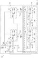
FIG. 1 shows an illustrative electronic device, in various examples. -
FIG. 2(a) shows an illustrative controller unit of an electronic device, in various examples. -
FIG. 2(b) shows another illustrative controller unit of an electronic device, in various examples. -
FIG. 3 shows an illustrative method for computing a sense current, in various examples. - Some power circuits employ power transistors that, in some cases, provide a current to a load (hereinafter referred to as load current). This load current is a large current (e.g., 10A), which, in some power system applications, such as electronic fuse (eFuse), needs to be measured. It is preferable to measure such a large-magnitude current indirectly, in contrast with the direct measurement of the load current, for example, using an ammeter. The indirect measurement may be done by coupling a sense transistor-which is smaller in size (e.g., smaller channel width) relative to the size of the power transistor-to the power transistor in such a fashion that when the power transistor is turned on, the sense transistor has a drain-source current (also referred herein as a sense current) indicative of the load current of the power transistor. Therefore, by measuring (or, in other words, sensing) the sense current, an indirect measurement can be made of the load current that is much larger in magnitude than the sense current. This indirect measurement is facilitated by using the sense transistor of a different size than the power transistor. The sizes can be chosen such that the load current relates to the sense current by a multiplicative factor. In some cases, this multiplicative factor is referred to as the sense ratio. Following sensing the sense current, the sense ratio can be multiplied with the sense current to compute the load current. A measurement circuit may be employed that is coupled to the power and sense transistors to measure (or sense) the sense current and compute the load current.
- The sense ratio may be represented as the ratio of resistances along the current flow paths of the sense transistor and power transistor, respectively. The resistance experienced by the current in sense and power transistors includes the parasitic resistance introduced because of the conducting properties of the materials used to fabricate the power and sense transistors. Furthermore, these parasitic resistances are different along the two current flow paths. Since resistance is a function of temperature, the parasitic resistances of both the power and sense transistors alter with temperature, but at different rates, which introduces error in the sense ratio, which further introduces error in measurement/computation of the load current. Stated another way, because the parasitic resistances of both the transistors vary differently with temperature, the sense ratio alters, thereby introducing error in the measured load current value as the sense current changes with temperature. Furthermore, the relationship of the sense current to the load current can vary as a function of the gate-to-source (VGS) bias provided to the power transistor.
- To mitigate the effect of parasitic resistance and/or gate bias upon the sense current for a power circuit comprising a sense transistor and a power transistor, in some examples, at least two sense transistors are coupled to a power transistor. Each of the at least two sense transistors couple to a different resistor (hereafter referred as compensation resistor) at their respective source terminals. These compensation resistors, at least in part, compensate for the error introduced in the sense current due to temperature and gate-to-source bias change. In at least some examples, the temperature coefficient of the compensation resistors is different. In some examples, as further described below, the load current of the power transistor can be computed, at least in part, using the known temperature coefficient values of the compensation resistors and the sense currents measured from the sense transistors. Compensation resistors with different temperature coefficients can be fabricated by using an element (e.g., metal), or by compounding different elements (e.g., polysilicon and metal). In some examples, one compensation resistor comprises polysilicon, and the other compensation resistor comprises metal. In other examples, one compensation resistor may comprise of both metal and polysilicon, and the other compensation resistor may comprise of metal. In other examples, various other combinations of one or more elements can be used to fabricate compensation resistors with different temperature coefficients. In at least some examples, the temperature coefficients' values can be quantified.
- Referring now to
FIG. 1 , an illustrativeelectronic device 100 is shown. Theelectronic device 100 includes apower transistor 104 that is integrated on asemiconductor die 102. Theelectronic device 100 also includessense transistors semiconductor die 102. In one example, thepower transistor 104 and thesense transistors power transistor 104 includes adrain terminal 104d, asource terminal 104s, and agate terminal 104g. Thesense transistor 106 includes adrain terminal 106d, a source terminal 106s, and agate terminal 106g. Thesense transistor 108 includes adrain terminal 108d, a source terminal 108s, and agate terminal 108g. Thedrain terminals node 111. - In some examples, the
power transistor 104 comprises a large number (e.g., on the order of 1000) of transistor cells integrated into thesemiconductor die 102 and coupled together in parallel such that thepower transistor 104 has a relatively large drain-source current when turned on. As noted above, in some examples, thesense transistors same semiconductor die 102, and are fabricated in the same process flow as thepower transistor 104. Thesense transistors power transistor 104. In some embodiments, thesense transistors semiconductor die 102 and coupled together in parallel, but where the parallel-connected transistor cells making up thesense transistors power transistor 104. In operation, when both thesense transistors power transistor 104 are turned on, the respective drain-source currents (i.e., the sense currents) of thesense transistors power transistor 104. - From a manufacturing and fabrication standpoint, in some examples, the
power transistor 104 and thesense transistors drain terminals semiconductor die 102, effectively coupling together their respective drain terminals. This coupled drain terminal is denoted asdrain terminal 110. This shared region of silicon can be referred to as a drain region in thesemiconductor die 102 for some examples in which power and sense transistors are nMOS transistors. Aresistor 105 and aresistor 107 represent a parasitic (and/or distributed) resistance of thedrain terminal 110. Let RSUB1 and RSUB2 denote, respectively, the resistance contributions of theresistors drain terminal 110. The sum of these two parasitic resistances, RSUB1 + RSUB2, is the total parasitic resistance of thedrain terminal 110. Stated another way, the circuit ofFIG. 1 shows thedrain terminals sense transistors node 111, indicating that theresistor 105 represents a parasitic resistance RSUB2 in common with both thepower transistor 104 and thesense transistors resistor 114 represents a parasitic resistance associated with thesource terminal 104s of thepower transistor 104. - A
resistor 106R has afirst terminal 135 coupled to thesource terminal 106d of thesense transistor 106, and a second terminal 136 coupled to a first node 120 of asub-controller 150 that is a part of acontroller 132. Thecontroller 132, in some examples, includes other added circuitry (not expressly shown inFIG. 1 ) that controls thegate terminal 104g of thetransistor 104. Thecontroller unit 132, in some examples, includes a processing unit (not expressly shown inFIG. 1 , but described below with respect toFIG. 2(a) ) and storage (e.g., RAM (random-access memory), ROM (read-only memory)), which may include any suitable type of non-transitory computer-readable medium storing machine-executable instructions. The machine-executable instructions, when executed by the processing unit, cause the processing unit to perform one or more of the actions attributed herein to thecontroller unit 132. Thecontroller unit 132 includes the first sub-controller 150 ("sub-controller 150") and a second sub-controller 160 ("sub-controller 160") that are coupled to thetransistors transistor 104, which, in turn, facilitates computing the drain-source current of thetransistor 104. In the particular example illustrated inFIG. 2 , thecontroller 132 is integrated on a second semiconductor die 118. In some examples, thecontroller 132 is integrated on the semiconductor die 102. - The sub-controller 150 includes a
node 138 is coupled to aterminal 112 of thepower transistor 104. The terminal 112 is coupled to thesource terminal 104s via theresistor 114. The sub-controller 150 is coupled to theresistor 106R to provide a virtual connection from theresistor 106R to theterminal 112 of thepower transistor 104. The sub-controller 150 includes anoperational amplifier 124 comprising afirst input port 139 coupled to theterminal 112 of thepower transistor 104, asecond input port 140 coupled to the second terminal 136 of theresistor 106R, and anoutput port 141. The sub-controller 150 further includes apass transistor 128 having agate terminal 128g, asource terminal 128s, and adrain terminal 128d. Thegate terminal 128g coupled to theoutput port 141 of theoperational amplifier 124, and asource terminal 128s coupled to the terminal 136 of theresistor 106R. The sub-controller 150 includes a negative feedback arrangement in which the sub-controller 150 is coupled to theresistor 106R and to theterminal 112 of thepower transistor 104 to maintain a first voltage at the first node 120 to substantially equal a second voltage at thenode 138. The sub-controller 150 causes only a negligible amount of current to flow from the second terminal 136 of theresistor 106R to theterminal 112 of thepower transistor 104, thereby providing a virtual connection between thenodes 138 and 120. - Similar to the
resistor 106R, aresistor 108R has afirst terminal 133 coupled to the source terminal 108s of thesense transistor 108, and a second terminal 134 coupled to a first node 122 of a sub-controller 160 that, as noted above, is a part of acontroller 132. The sub-controller 160 includes anode 144 coupled to theterminal 112 of thepower transistor 104. The sub-controller 160 is coupled to theresistor 108R to provide a virtual connection from theresistor 108R to theterminal 112 of thepower transistor 104. The sub-controller 160 includes anoperational amplifier 126 comprising afirst input port 146 coupled to theterminal 112 of thepower transistor 104, asecond input port 148 coupled to thesecond terminal 124 of theresistor 108R, and anoutput port 151. The sub-controller 160 further includes apass transistor 130 having agate terminal 130g, asource terminal 130s, and adrain terminal 130d. Thegate terminal 130g coupled to theoutput port 151 of theoperational amplifier 126, and asource terminal 130s coupled to the terminal 134 of theresistor 108R. The sub-controller 160 includes a negative feedback arrangement in which the sub-controller 160 is coupled to theresistor 108R and to theterminal 112 of thepower transistor 104 to maintain a first voltage at the first node 122 to substantially equal a second voltage at thenode 144. The sub-controller 160 causes only a negligible amount of current to flow from the second terminal 134 of theresistor 108R to theterminal 112 of thepower transistor 104, thereby providing a virtual connection between thenodes 144 and 122. - The
resistors resistors resistor 106R can be fabricated by using an element (e.g., metal), or by compounding different elements (e.g., polysilicon and metal). The temperature coefficient of theresistor 106R can be notated by TC106. On the other hand, theresistor 108R can be fabricated using different combinations of one or more elements such that the resulting temperature coefficient of theresistor 108R is different than the temperature coefficient of theresistor 106R. The temperature coefficient of theresistor 108R can be notated by TC108, and the temperature coefficients TC106 and TC108 are unequal. In at least some examples, theresistors controller unit 132. In some scenarios, the stored values of the temperature coefficients need to be corrected because temperature coefficients may vary over time, or due to some other reason. In such scenarios, thecontroller unit 132 may be configured to auto-correct the temperature coefficient values by using, at least in part, equation 1 described below. - The load current is a product of the sense ratio and the sense current, and the sense ratio, as noted above, is the ratio of the resistance seen by the sense current to the resistance seen by the load current. Therefore, the sense current Isns can be expressed as

controller unit 132, and the sensed current is adjusted (or, in some examples, auto-corrected) for temperature variations. - As noted above, the sub-controller 150 causes only a negligible amount of current to flow from the second terminal 136 of the
resistor 106R to theterminal 112 of thepower transistor 104, thereby providing a virtual connection between thenodes 138 and 120. Similarly, sub-controller 160 causes only a negligible amount of current to flow from the second terminal 134 of theresistor 108R to theterminal 112 of thepower transistor 104, thereby providing a virtual connection between the nodes 138 (or the node 144) and 122. Stated another way, the voltage potential at node 120 and the voltage potential atnode 138 is substantially similar; and the voltage potential at node 122 and the voltage potential atnode 144 are substantially similar. Referring now to the operation of theelectronic device 100, as thetransistor 104 is turned on (by a gate signal sent via the controller unit 132), the load current flows from the transistor 104 (depending on the drain-to-source voltage). Thetransistors transistor 104 such that a current mirroring the load current flows from thetransistors operational amplifiers transistors pass transistors pass transistors transistors sub-controllers node operational amplifiers power transistor 104 and thesense transistors operational amplifier pass transistors - In some of the examples described above, the
transistors transistors transistors FIG. 1 , thepass transistors transistors - Referring now to
FIG. 2(a) , anillustrative controller unit 132 is shown. Thecontroller unit 132 facilitates computing a desired sense current, which, in-turn, facilitates computing the drain-to-source current of the power transistor. Thecontroller unit 132, in one example, includes a processing unit (hereinafter "processor") 205, a memory unit (hereinafter "memory") 210 coupled to theprocessor 205. Thecurrent measuring unit 206 couples to theprocessor 205. In some examples,memory 210 includes RAM (random-access memory, and ROM (read-only memory). In some examples,memory 210 includes any suitable type of non-transitory computer-readable medium storing machine-executable instructions. The machine-executable instructions, when executed by theprocessor 205, cause theprocessor 205 to perform one or more of the actions attributed herein to thecontroller unit 132. The sub-controllers 150, 160 couple to thecurrent measuring unit 206 viaconductors current measuring unit 206 includes one or more resistors of known values that are configured to convert the sense current ISNS1, ISNS2 to voltages VSNS1 and VSNS2. These voltages may further be digitized using analog-to-digital converters-whose output can be processed in thecontroller unit 132. - The
processor 205 is configured to compute the desired sense current ISNS0, and, in-turn, compute the drain-to-source current of thetransistor 104. Referring now toFIG. 3 , anillustrative method 300 for computing the desired sense current ISNS0 is shown. Themethod 300 begins with astep 305 that includes measuring the first sense current ISNS1 and a second sense current ISNS2. This is done by thecurrent measuring unit 206 present in thecontroller unit 132. Following the current measurement, the measured values may be communicated to theprocessor 205, or in some examples, stored in thememory 210. Themethod 300 then moves to thestep 310 that includes computing the desired sense current ISNS0. In some examples, this computation is performed by using a current-temperature relationship that defines first and second currents as:

sub-controllers memory 210. ΔT can be computed by theprocessor 205 using equation 3 depicted below:

- Following computing the desired current sense ISNS0, the
method 300 moves to astep 315 that includes computing the drain-to-source current of thetransistor 104. This is done by using the pre-defined sense ratio value and the desired current sense ISNS0 value. For example, assuming the sense ration is defined by "SR," the drain-to-source current of thetransistor 104 is SR x ISNS0. Themethod 300, in some examples, then moves to thestep 320 that includes comparing the drain-to-source current value with a threshold value. If the drain-to-source current value is higher than the threshold, thecontroller unit 132 performs an action based on the comparison. For example, in eFuse applications, thecontroller unit 132 may be configured to turn-off the current flow in a situation where flow of current in an electrical system is equal to or more than a rated (e.g., threshold) value. - Some examples of the
controller unit 132 may include analog circuitry to generate the desired sense current ISNS0 value, which, in turn, may be used to compute the drain-to-source current of thetransistor 104. Referring now toFIG. 2(b) , anillustrative controller unit 132 is shown that includes a weighted average technique to compute the desired sense current ISNS0. In some examples, such technique includesresistors additional resistors resistors nodes resistors resistors node 219, which further couples to anoperational amplifier 232 via aconductor 230. Theoperational amplifier 232 includes a feedback resistor 244. In the example depicted inFIG. 2(b) , the negative terminal of theoperational amplifier 232 is coupled to a ground source (or a virtual ground source) via aterminal 225 and/or aresistor 233. An output Vout of theoperational amplifier 232 can be computed by the following weighted averaged equation: Vout = R1ISNS1 + R2ISNS2. This output Vout may further be digitized using analog-to-digital converters, and the digitized data may be processed in a processor (not expressly depicted) similar to theprocessor 205. - In the foregoing discussion and in the claims, the terms "including" and "comprising" are used in an open-ended fashion, and thus should be interpreted to mean "including, but not limited to...." Also, the term "couple" or "couples" is intended to mean either an indirect or direct connection. An element or feature that is "configured to" perform a task or function may be configured (e.g., programmed or structurally designed) at a time of manufacturing by a manufacturer to perform the function and/or may be configurable (or re-configurable) by a user after manufacturing to perform the function and/or other additional or alternative functions. The configuring may be through firmware and/or software programming of the device, through a construction and/or layout of hardware components and interconnections of the device, or a combination thereof. Also, uses of the phrases "ground" or similar in the foregoing discussion are intended to include a chassis ground, an Earth ground, a floating ground, a virtual ground, a digital ground, a common ground, and/or any other form of ground connection applicable to, or suitable for, the teachings of the description. Unless otherwise stated, "about," "approximately," or "substantially" preceding a value means +/- 10 percent of the stated value.
- The above discussion is meant to be illustrative of the principles and various embodiments. Numerous variations and modifications will become apparent to those skilled in the art once the above description is fully appreciated. The invention is defined by the features of independent claims. Preferred embodiments are set out in the dependent claims.
Claims (7)
- An electronic fuse (eFuse), comprising:a controller;a power transistor (104) configured to conduct a load current between a first terminal anda second terminal of the power transistor, wherein the first terminal couples to the controller at a first node;a first sense transistor (106) coupled to the power transistor at the second terminal, whereina third terminal of the first sense transistor couples to the controller via a first resistor (106R) ata second node, the first resistor having a first temperature coefficient; anda second sense transistor (108) coupled to the power transistor at the second terminal,wherein a fourth terminal of the second sense transistor couples to the controller via a second resistor (108R) at a third node, the second resistor having a second temperature coefficient,wherein the controller is configured to generate a first sense current that is a function of the first temperature coefficient and a second sense current that is a function of the second temperature coefficient;wherein the controller is configured to compute a desired current value using the first and the second sense currents;wherein the controller is configured to turn-off an electrical system if the controller determines that the desired current value is greater than a pre-defined value; andwherein the first and second temperature coefficients are different.
- The eFuse of claim 1, wherein the power, first sense, and second sense transistors are each n-metal-oxide-semiconductor field-effect-transistors (nMOSFETs);
or, wherein the power, first sense, and second sense transistors are each p-metal-oxide-semiconductor field-effect-transistors (pMOSFETs). - The eFuse of claim 1, wherein the controller is configured to provide a virtual connection from the first terminal to the third terminal and a virtual connection from the first terminal to the fourth terminal.
- The eFuse of claim 1, the controller is configured to maintain a first voltage at the first node that substantially equals a second voltage at the second node and a third voltage at the third node.
- The eFuse of claim 1, wherein the power transistor, the first sense transistor, the second sense transistor, the first resistor, and the second resistor are integrated in a first semiconductor die; and wherein the controller unit is integrated in a second semiconductor die.
- The eFuse of claim 1, wherein the desired sense current is a scaled-down version of a current flowing between the first terminal and the second terminal
- A method of operating an electronic fuse according to the claims 1-6, comprising:measuring, by a controller, a first sense current and a second sense current, wherein the first sense current is received via a first sense transistor, and the second sense current is received via a second sense transistor, wherein the first and second sense transistors couple to a power transistor, wherein the first sense transistor couples to the controller via a first resistor and the second sense transistor couples to the controller via a second resistor;computing, by the controller, a desired sense current value using the first and second sense currents; andcomputing, by the controller, a load current flowing via the power transistor using the desired sense current value;comparing, by the controller, the load current with a threshold value; andfacilitating turning-off an electrical system based on the determination that the load current is higher than or equal to the threshold value;wherein the first resistor has a first temperature coefficient and the second resistor has a second temperature coefficient, and wherein the first and second temperature coefficients are different.
Applications Claiming Priority (2)
| Application Number | Priority Date | Filing Date | Title |
|---|---|---|---|
| US16/050,383 US10679938B2 (en) | 2018-07-31 | 2018-07-31 | Power transistor coupled to multiple sense transistors |
| PCT/US2019/044024 WO2020028291A1 (en) | 2018-07-31 | 2019-07-30 | Power transistor coupled to multiple sense transistors |
Publications (3)
| Publication Number | Publication Date |
|---|---|
| EP3830870A1 EP3830870A1 (en) | 2021-06-09 |
| EP3830870A4 EP3830870A4 (en) | 2021-08-25 |
| EP3830870B1 true EP3830870B1 (en) | 2024-06-19 |
Family
ID=69227554
Family Applications (1)
| Application Number | Title | Priority Date | Filing Date |
|---|---|---|---|
| EP19843646.1A Active EP3830870B1 (en) | 2018-07-31 | 2019-07-30 | Power transistor coupled to multiple sense transistors |
Country Status (5)
| Country | Link |
|---|---|
| US (1) | US10679938B2 (en) |
| EP (1) | EP3830870B1 (en) |
| JP (1) | JP7532714B2 (en) |
| CN (1) | CN113169155B (en) |
| WO (1) | WO2020028291A1 (en) |
Families Citing this family (1)
| Publication number | Priority date | Publication date | Assignee | Title |
|---|---|---|---|---|
| JP7830854B2 (en) * | 2021-08-27 | 2026-03-17 | 三菱ケミカル株式会社 | Epoxy resin sheets, laminates, stretchable members, flexible members, and winding bodies |
Citations (1)
| Publication number | Priority date | Publication date | Assignee | Title |
|---|---|---|---|---|
| EP0428813B1 (en) * | 1989-11-17 | 1995-02-01 | STMicroelectronics S.r.l. | Nevice for protection against the short circuit of a MOS-type power device, with a preset dependance on the temperature at which the power device operates |
Family Cites Families (18)
| Publication number | Priority date | Publication date | Assignee | Title |
|---|---|---|---|---|
| DE3906955C1 (en) | 1989-03-04 | 1990-07-19 | Daimler-Benz Aktiengesellschaft, 7000 Stuttgart, De | Electronic fuse (safety device) for a transistor output stage |
| JPH05299431A (en) * | 1992-04-16 | 1993-11-12 | Toyota Autom Loom Works Ltd | Transistor with current detecting function attached |
| JP3780926B2 (en) | 2001-12-06 | 2006-05-31 | 株式会社デンソー | Load drive circuit |
| US7099135B2 (en) * | 2002-11-05 | 2006-08-29 | Semiconductor Components Industries, L.L.C | Integrated inrush current limiter circuit and method |
| US6943069B2 (en) | 2003-10-14 | 2005-09-13 | Semiconductor Components Industries, L.L.C. | Power system inhibit method and device and structure therefor |
| KR100786768B1 (en) | 2005-11-11 | 2007-12-18 | 경상대학교산학협력단 | Apparatus and method for regulating semiconductor well voltage |
| KR101537534B1 (en) * | 2008-12-31 | 2015-07-17 | 주식회사 동부하이텍 | Current sensing circuit |
| US7852148B2 (en) * | 2009-03-27 | 2010-12-14 | Semiconductor Components Industries, Llc | Method of forming a sensing circuit and structure therefor |
| US9634081B2 (en) * | 2013-10-08 | 2017-04-25 | Infineon Technologies Ag | Methods for producing polysilicon resistors |
| EP2942851B1 (en) | 2014-05-09 | 2016-07-13 | dSPACE digital signal processing and control engineering GmbH | Method for monitoring the power consumption of an electrical consumer |
| JP6396730B2 (en) * | 2014-09-19 | 2018-09-26 | ルネサスエレクトロニクス株式会社 | Semiconductor device |
| JP5905622B2 (en) | 2015-04-13 | 2016-04-20 | ルネサスエレクトロニクス株式会社 | Semiconductor device |
| US9804205B2 (en) * | 2015-04-27 | 2017-10-31 | Power Integrations, Inc. | Current sense ratio compensation |
| CN105242190B (en) | 2015-10-19 | 2018-11-27 | 矽力杰半导体技术(杭州)有限公司 | current detection circuit |
| JP6594810B2 (en) * | 2016-03-23 | 2019-10-23 | ルネサスエレクトロニクス株式会社 | Current detection circuit and DCDC converter having the same |
| US10637229B2 (en) | 2016-09-02 | 2020-04-28 | Magna Electronics Inc. | Electronic fuse module with built in microcontroller and centralized power management bus |
| US11196250B2 (en) * | 2017-10-20 | 2021-12-07 | Texas Instruments Incorporated | Bidirectional precision surge clamp with near-zero dynamic resistance and ultra-low leakage current |
| US10422818B2 (en) * | 2017-12-30 | 2019-09-24 | Texas Instruments Incorporated | Power transistors with a resistor coupled to a sense transistor |
-
2018
- 2018-07-31 US US16/050,383 patent/US10679938B2/en active Active
-
2019
- 2019-07-30 JP JP2021505704A patent/JP7532714B2/en active Active
- 2019-07-30 WO PCT/US2019/044024 patent/WO2020028291A1/en not_active Ceased
- 2019-07-30 CN CN201980051009.6A patent/CN113169155B/en active Active
- 2019-07-30 EP EP19843646.1A patent/EP3830870B1/en active Active
Patent Citations (1)
| Publication number | Priority date | Publication date | Assignee | Title |
|---|---|---|---|---|
| EP0428813B1 (en) * | 1989-11-17 | 1995-02-01 | STMicroelectronics S.r.l. | Nevice for protection against the short circuit of a MOS-type power device, with a preset dependance on the temperature at which the power device operates |
Also Published As
| Publication number | Publication date |
|---|---|
| WO2020028291A1 (en) | 2020-02-06 |
| CN113169155A (en) | 2021-07-23 |
| EP3830870A1 (en) | 2021-06-09 |
| JP2021532600A (en) | 2021-11-25 |
| US20200043849A1 (en) | 2020-02-06 |
| JP7532714B2 (en) | 2024-08-14 |
| CN113169155B (en) | 2025-03-11 |
| US10679938B2 (en) | 2020-06-09 |
| WO2020028291A8 (en) | 2021-06-17 |
| EP3830870A4 (en) | 2021-08-25 |
Similar Documents
| Publication | Publication Date | Title |
|---|---|---|
| US8450986B2 (en) | Voltage regulator | |
| US7411376B2 (en) | Voltage regulator having overcurrent protection circuit and method manufacturing voltage regulator | |
| US7636009B2 (en) | Bias current generating apparatus with adjustable temperature coefficient | |
| US8497791B2 (en) | Operational amplifier | |
| US9618951B2 (en) | Voltage regulator | |
| US20050029999A1 (en) | Voltage regulator | |
| US8648585B2 (en) | Circuit including first and second transistors coupled between an outpout terminal and a power supply | |
| US9372489B2 (en) | Voltage regulator having a temperature sensitive leakage current sink circuit | |
| TWI743334B (en) | Overcurrent protection circuit and voltage regulator | |
| US8493702B2 (en) | Current limiting circuit | |
| KR102227586B1 (en) | Voltage regulator | |
| US8040650B2 (en) | Excess-current protection circuit and power supply | |
| US10007283B2 (en) | Voltage regulator | |
| EP3320349B1 (en) | Apparatus and method for measuring load current by applying compensated gain to voltage derived from drain-to-source voltage of power gating device | |
| JPH0949858A (en) | Current detection control circuit and pattern layout method | |
| US10754369B2 (en) | Reference current source and semiconductor device | |
| JP5136144B2 (en) | Load current supply circuit | |
| US10679938B2 (en) | Power transistor coupled to multiple sense transistors | |
| US8415971B2 (en) | Transceiving circuit and transceiving circuit resistance calibration method | |
| US20100295528A1 (en) | Circuit for direct gate drive current reference source | |
| US11948708B2 (en) | Resistance device and current detection circuit including the resistance device | |
| US11387825B2 (en) | Overheat protection circuit and semiconductor device including the same | |
| US10422818B2 (en) | Power transistors with a resistor coupled to a sense transistor | |
| JP2022174431A (en) | constant current circuit | |
| CN111697955A (en) | Semiconductor integrated circuit and power supply system |
Legal Events
| Date | Code | Title | Description |
|---|---|---|---|
| STAA | Information on the status of an ep patent application or granted ep patent |
Free format text: STATUS: THE INTERNATIONAL PUBLICATION HAS BEEN MADE |
|
| PUAI | Public reference made under article 153(3) epc to a published international application that has entered the european phase |
Free format text: ORIGINAL CODE: 0009012 |
|
| STAA | Information on the status of an ep patent application or granted ep patent |
Free format text: STATUS: REQUEST FOR EXAMINATION WAS MADE |
|
| 17P | Request for examination filed |
Effective date: 20210301 |
|
| AK | Designated contracting states |
Kind code of ref document: A1 Designated state(s): AL AT BE BG CH CY CZ DE DK EE ES FI FR GB GR HR HU IE IS IT LI LT LU LV MC MK MT NL NO PL PT RO RS SE SI SK SM TR |
|
| RAP3 | Party data changed (applicant data changed or rights of an application transferred) |
Owner name: TEXAS INSTRUMENTS INCORPORATED |
|
| RIN1 | Information on inventor provided before grant (corrected) |
Inventor name: JOARDAR, KUNTAL Inventor name: CHU, MIN Inventor name: KRISHNAMURTHY, VIJAY Inventor name: HARJONO, TIKNO Inventor name: CHAUHAN, ANKUR Inventor name: HEGDE, VINAYAK Inventor name: SRIVASTAVA, MANISH |
|
| A4 | Supplementary search report drawn up and despatched |
Effective date: 20210722 |
|
| RIC1 | Information provided on ipc code assigned before grant |
Ipc: H01L 25/00 20060101AFI20210716BHEP Ipc: G01R 19/00 20060101ALI20210716BHEP Ipc: H03K 17/082 20060101ALI20210716BHEP Ipc: H03K 17/14 20060101ALI20210716BHEP |
|
| DAV | Request for validation of the european patent (deleted) | ||
| DAX | Request for extension of the european patent (deleted) | ||
| GRAP | Despatch of communication of intention to grant a patent |
Free format text: ORIGINAL CODE: EPIDOSNIGR1 |
|
| STAA | Information on the status of an ep patent application or granted ep patent |
Free format text: STATUS: GRANT OF PATENT IS INTENDED |
|
| INTG | Intention to grant announced |
Effective date: 20240202 |
|
| GRAS | Grant fee paid |
Free format text: ORIGINAL CODE: EPIDOSNIGR3 |
|
| GRAA | (expected) grant |
Free format text: ORIGINAL CODE: 0009210 |
|
| STAA | Information on the status of an ep patent application or granted ep patent |
Free format text: STATUS: THE PATENT HAS BEEN GRANTED |
|
| P01 | Opt-out of the competence of the unified patent court (upc) registered |
Effective date: 20240415 |
|
| AK | Designated contracting states |
Kind code of ref document: B1 Designated state(s): AL AT BE BG CH CY CZ DE DK EE ES FI FR GB GR HR HU IE IS IT LI LT LU LV MC MK MT NL NO PL PT RO RS SE SI SK SM TR |
|
| REG | Reference to a national code |
Ref country code: GB Ref legal event code: FG4D |
|
| REG | Reference to a national code |
Ref country code: CH Ref legal event code: EP |
|
| REG | Reference to a national code |
Ref country code: DE Ref legal event code: R096 Ref document number: 602019053983 Country of ref document: DE |
|
| PG25 | Lapsed in a contracting state [announced via postgrant information from national office to epo] |
Ref country code: BG Free format text: LAPSE BECAUSE OF FAILURE TO SUBMIT A TRANSLATION OF THE DESCRIPTION OR TO PAY THE FEE WITHIN THE PRESCRIBED TIME-LIMIT Effective date: 20240619 |
|
| PG25 | Lapsed in a contracting state [announced via postgrant information from national office to epo] |
Ref country code: HR Free format text: LAPSE BECAUSE OF FAILURE TO SUBMIT A TRANSLATION OF THE DESCRIPTION OR TO PAY THE FEE WITHIN THE PRESCRIBED TIME-LIMIT Effective date: 20240619 Ref country code: FI Free format text: LAPSE BECAUSE OF FAILURE TO SUBMIT A TRANSLATION OF THE DESCRIPTION OR TO PAY THE FEE WITHIN THE PRESCRIBED TIME-LIMIT Effective date: 20240619 |
|
| REG | Reference to a national code |
Ref country code: LT Ref legal event code: MG9D |
|
| PG25 | Lapsed in a contracting state [announced via postgrant information from national office to epo] |
Ref country code: GR Free format text: LAPSE BECAUSE OF FAILURE TO SUBMIT A TRANSLATION OF THE DESCRIPTION OR TO PAY THE FEE WITHIN THE PRESCRIBED TIME-LIMIT Effective date: 20240920 |
|
| REG | Reference to a national code |
Ref country code: NL Ref legal event code: MP Effective date: 20240619 |
|
| PG25 | Lapsed in a contracting state [announced via postgrant information from national office to epo] |
Ref country code: LV Free format text: LAPSE BECAUSE OF FAILURE TO SUBMIT A TRANSLATION OF THE DESCRIPTION OR TO PAY THE FEE WITHIN THE PRESCRIBED TIME-LIMIT Effective date: 20240619 |
|
| PG25 | Lapsed in a contracting state [announced via postgrant information from national office to epo] |
Ref country code: NO Free format text: LAPSE BECAUSE OF FAILURE TO SUBMIT A TRANSLATION OF THE DESCRIPTION OR TO PAY THE FEE WITHIN THE PRESCRIBED TIME-LIMIT Effective date: 20240919 Ref country code: LV Free format text: LAPSE BECAUSE OF FAILURE TO SUBMIT A TRANSLATION OF THE DESCRIPTION OR TO PAY THE FEE WITHIN THE PRESCRIBED TIME-LIMIT Effective date: 20240619 Ref country code: HR Free format text: LAPSE BECAUSE OF FAILURE TO SUBMIT A TRANSLATION OF THE DESCRIPTION OR TO PAY THE FEE WITHIN THE PRESCRIBED TIME-LIMIT Effective date: 20240619 Ref country code: GR Free format text: LAPSE BECAUSE OF FAILURE TO SUBMIT A TRANSLATION OF THE DESCRIPTION OR TO PAY THE FEE WITHIN THE PRESCRIBED TIME-LIMIT Effective date: 20240920 Ref country code: FI Free format text: LAPSE BECAUSE OF FAILURE TO SUBMIT A TRANSLATION OF THE DESCRIPTION OR TO PAY THE FEE WITHIN THE PRESCRIBED TIME-LIMIT Effective date: 20240619 Ref country code: BG Free format text: LAPSE BECAUSE OF FAILURE TO SUBMIT A TRANSLATION OF THE DESCRIPTION OR TO PAY THE FEE WITHIN THE PRESCRIBED TIME-LIMIT Effective date: 20240619 Ref country code: RS Free format text: LAPSE BECAUSE OF FAILURE TO SUBMIT A TRANSLATION OF THE DESCRIPTION OR TO PAY THE FEE WITHIN THE PRESCRIBED TIME-LIMIT Effective date: 20240919 |
|
| PG25 | Lapsed in a contracting state [announced via postgrant information from national office to epo] |
Ref country code: NL Free format text: LAPSE BECAUSE OF FAILURE TO SUBMIT A TRANSLATION OF THE DESCRIPTION OR TO PAY THE FEE WITHIN THE PRESCRIBED TIME-LIMIT Effective date: 20240619 |
|
| REG | Reference to a national code |
Ref country code: AT Ref legal event code: MK05 Ref document number: 1696519 Country of ref document: AT Kind code of ref document: T Effective date: 20240619 |
|
| PG25 | Lapsed in a contracting state [announced via postgrant information from national office to epo] |
Ref country code: NL Free format text: LAPSE BECAUSE OF FAILURE TO SUBMIT A TRANSLATION OF THE DESCRIPTION OR TO PAY THE FEE WITHIN THE PRESCRIBED TIME-LIMIT Effective date: 20240619 |
|
| PG25 | Lapsed in a contracting state [announced via postgrant information from national office to epo] |
Ref country code: PT Free format text: LAPSE BECAUSE OF FAILURE TO SUBMIT A TRANSLATION OF THE DESCRIPTION OR TO PAY THE FEE WITHIN THE PRESCRIBED TIME-LIMIT Effective date: 20241021 |
|
| PG25 | Lapsed in a contracting state [announced via postgrant information from national office to epo] |
Ref country code: PT Free format text: LAPSE BECAUSE OF FAILURE TO SUBMIT A TRANSLATION OF THE DESCRIPTION OR TO PAY THE FEE WITHIN THE PRESCRIBED TIME-LIMIT Effective date: 20241021 |
|
| PG25 | Lapsed in a contracting state [announced via postgrant information from national office to epo] |
Ref country code: PL Free format text: LAPSE BECAUSE OF FAILURE TO SUBMIT A TRANSLATION OF THE DESCRIPTION OR TO PAY THE FEE WITHIN THE PRESCRIBED TIME-LIMIT Effective date: 20240619 |
|
| PG25 | Lapsed in a contracting state [announced via postgrant information from national office to epo] |
Ref country code: EE Free format text: LAPSE BECAUSE OF FAILURE TO SUBMIT A TRANSLATION OF THE DESCRIPTION OR TO PAY THE FEE WITHIN THE PRESCRIBED TIME-LIMIT Effective date: 20240619 |
|
| PG25 | Lapsed in a contracting state [announced via postgrant information from national office to epo] |
Ref country code: AT Free format text: LAPSE BECAUSE OF FAILURE TO SUBMIT A TRANSLATION OF THE DESCRIPTION OR TO PAY THE FEE WITHIN THE PRESCRIBED TIME-LIMIT Effective date: 20240619 Ref country code: IS Free format text: LAPSE BECAUSE OF FAILURE TO SUBMIT A TRANSLATION OF THE DESCRIPTION OR TO PAY THE FEE WITHIN THE PRESCRIBED TIME-LIMIT Effective date: 20241019 |
|
| PG25 | Lapsed in a contracting state [announced via postgrant information from national office to epo] |
Ref country code: CZ Free format text: LAPSE BECAUSE OF FAILURE TO SUBMIT A TRANSLATION OF THE DESCRIPTION OR TO PAY THE FEE WITHIN THE PRESCRIBED TIME-LIMIT Effective date: 20240619 |
|
| PG25 | Lapsed in a contracting state [announced via postgrant information from national office to epo] |
Ref country code: RO Free format text: LAPSE BECAUSE OF FAILURE TO SUBMIT A TRANSLATION OF THE DESCRIPTION OR TO PAY THE FEE WITHIN THE PRESCRIBED TIME-LIMIT Effective date: 20240619 Ref country code: SK Free format text: LAPSE BECAUSE OF FAILURE TO SUBMIT A TRANSLATION OF THE DESCRIPTION OR TO PAY THE FEE WITHIN THE PRESCRIBED TIME-LIMIT Effective date: 20240619 |
|
| PG25 | Lapsed in a contracting state [announced via postgrant information from national office to epo] |
Ref country code: ES Free format text: LAPSE BECAUSE OF FAILURE TO SUBMIT A TRANSLATION OF THE DESCRIPTION OR TO PAY THE FEE WITHIN THE PRESCRIBED TIME-LIMIT Effective date: 20240619 Ref country code: SM Free format text: LAPSE BECAUSE OF FAILURE TO SUBMIT A TRANSLATION OF THE DESCRIPTION OR TO PAY THE FEE WITHIN THE PRESCRIBED TIME-LIMIT Effective date: 20240619 |
|
| PG25 | Lapsed in a contracting state [announced via postgrant information from national office to epo] |
Ref country code: SM Free format text: LAPSE BECAUSE OF FAILURE TO SUBMIT A TRANSLATION OF THE DESCRIPTION OR TO PAY THE FEE WITHIN THE PRESCRIBED TIME-LIMIT Effective date: 20240619 Ref country code: SK Free format text: LAPSE BECAUSE OF FAILURE TO SUBMIT A TRANSLATION OF THE DESCRIPTION OR TO PAY THE FEE WITHIN THE PRESCRIBED TIME-LIMIT Effective date: 20240619 Ref country code: RO Free format text: LAPSE BECAUSE OF FAILURE TO SUBMIT A TRANSLATION OF THE DESCRIPTION OR TO PAY THE FEE WITHIN THE PRESCRIBED TIME-LIMIT Effective date: 20240619 Ref country code: PL Free format text: LAPSE BECAUSE OF FAILURE TO SUBMIT A TRANSLATION OF THE DESCRIPTION OR TO PAY THE FEE WITHIN THE PRESCRIBED TIME-LIMIT Effective date: 20240619 Ref country code: IS Free format text: LAPSE BECAUSE OF FAILURE TO SUBMIT A TRANSLATION OF THE DESCRIPTION OR TO PAY THE FEE WITHIN THE PRESCRIBED TIME-LIMIT Effective date: 20241019 Ref country code: ES Free format text: LAPSE BECAUSE OF FAILURE TO SUBMIT A TRANSLATION OF THE DESCRIPTION OR TO PAY THE FEE WITHIN THE PRESCRIBED TIME-LIMIT Effective date: 20240619 Ref country code: EE Free format text: LAPSE BECAUSE OF FAILURE TO SUBMIT A TRANSLATION OF THE DESCRIPTION OR TO PAY THE FEE WITHIN THE PRESCRIBED TIME-LIMIT Effective date: 20240619 Ref country code: CZ Free format text: LAPSE BECAUSE OF FAILURE TO SUBMIT A TRANSLATION OF THE DESCRIPTION OR TO PAY THE FEE WITHIN THE PRESCRIBED TIME-LIMIT Effective date: 20240619 Ref country code: AT Free format text: LAPSE BECAUSE OF FAILURE TO SUBMIT A TRANSLATION OF THE DESCRIPTION OR TO PAY THE FEE WITHIN THE PRESCRIBED TIME-LIMIT Effective date: 20240619 |
|
| PG25 | Lapsed in a contracting state [announced via postgrant information from national office to epo] |
Ref country code: IT Free format text: LAPSE BECAUSE OF FAILURE TO SUBMIT A TRANSLATION OF THE DESCRIPTION OR TO PAY THE FEE WITHIN THE PRESCRIBED TIME-LIMIT Effective date: 20240619 |
|
| REG | Reference to a national code |
Ref country code: CH Ref legal event code: PL |
|
| PG25 | Lapsed in a contracting state [announced via postgrant information from national office to epo] |
Ref country code: LU Free format text: LAPSE BECAUSE OF NON-PAYMENT OF DUE FEES Effective date: 20240730 |
|
| PG25 | Lapsed in a contracting state [announced via postgrant information from national office to epo] |
Ref country code: MC Free format text: LAPSE BECAUSE OF FAILURE TO SUBMIT A TRANSLATION OF THE DESCRIPTION OR TO PAY THE FEE WITHIN THE PRESCRIBED TIME-LIMIT Effective date: 20240619 |
|
| REG | Reference to a national code |
Ref country code: DE Ref legal event code: R097 Ref document number: 602019053983 Country of ref document: DE |
|
| PG25 | Lapsed in a contracting state [announced via postgrant information from national office to epo] |
Ref country code: MC Free format text: LAPSE BECAUSE OF FAILURE TO SUBMIT A TRANSLATION OF THE DESCRIPTION OR TO PAY THE FEE WITHIN THE PRESCRIBED TIME-LIMIT Effective date: 20240619 Ref country code: LU Free format text: LAPSE BECAUSE OF NON-PAYMENT OF DUE FEES Effective date: 20240730 |
|
| PG25 | Lapsed in a contracting state [announced via postgrant information from national office to epo] |
Ref country code: DK Free format text: LAPSE BECAUSE OF FAILURE TO SUBMIT A TRANSLATION OF THE DESCRIPTION OR TO PAY THE FEE WITHIN THE PRESCRIBED TIME-LIMIT Effective date: 20240619 |
|
| PG25 | Lapsed in a contracting state [announced via postgrant information from national office to epo] |
Ref country code: BE Free format text: LAPSE BECAUSE OF NON-PAYMENT OF DUE FEES Effective date: 20240731 Ref country code: CH Free format text: LAPSE BECAUSE OF NON-PAYMENT OF DUE FEES Effective date: 20240731 |
|
| PLBE | No opposition filed within time limit |
Free format text: ORIGINAL CODE: 0009261 |
|
| STAA | Information on the status of an ep patent application or granted ep patent |
Free format text: STATUS: NO OPPOSITION FILED WITHIN TIME LIMIT |
|
| 26N | No opposition filed |
Effective date: 20250320 |
|
| REG | Reference to a national code |
Ref country code: BE Ref legal event code: MM Effective date: 20240731 |
|
| PGFP | Annual fee paid to national office [announced via postgrant information from national office to epo] |
Ref country code: GB Payment date: 20250619 Year of fee payment: 7 |
|
| PGFP | Annual fee paid to national office [announced via postgrant information from national office to epo] |
Ref country code: FR Payment date: 20250619 Year of fee payment: 7 |
|
| PG25 | Lapsed in a contracting state [announced via postgrant information from national office to epo] |
Ref country code: IE Free format text: LAPSE BECAUSE OF NON-PAYMENT OF DUE FEES Effective date: 20240730 |
|
| PG25 | Lapsed in a contracting state [announced via postgrant information from national office to epo] |
Ref country code: SE Free format text: LAPSE BECAUSE OF FAILURE TO SUBMIT A TRANSLATION OF THE DESCRIPTION OR TO PAY THE FEE WITHIN THE PRESCRIBED TIME-LIMIT Effective date: 20240619 |
|
| PGFP | Annual fee paid to national office [announced via postgrant information from national office to epo] |
Ref country code: DE Payment date: 20250620 Year of fee payment: 7 |
|
| REG | Reference to a national code |
Ref country code: DE Ref legal event code: R079 Ref document number: 602019053983 Country of ref document: DE Free format text: PREVIOUS MAIN CLASS: H01L0025000000 Ipc: H10W0090000000 |
|
| PG25 | Lapsed in a contracting state [announced via postgrant information from national office to epo] |
Ref country code: CY Free format text: LAPSE BECAUSE OF FAILURE TO SUBMIT A TRANSLATION OF THE DESCRIPTION OR TO PAY THE FEE WITHIN THE PRESCRIBED TIME-LIMIT; INVALID AB INITIO Effective date: 20190730 |
|
| PG25 | Lapsed in a contracting state [announced via postgrant information from national office to epo] |
Ref country code: HU Free format text: LAPSE BECAUSE OF FAILURE TO SUBMIT A TRANSLATION OF THE DESCRIPTION OR TO PAY THE FEE WITHIN THE PRESCRIBED TIME-LIMIT; INVALID AB INITIO Effective date: 20190730 |