EP0428813A1 - Nevice for protection against the short circuit of a MOS-type power device, with a preset dependance on the temperature at which the power device operates - Google Patents
Nevice for protection against the short circuit of a MOS-type power device, with a preset dependance on the temperature at which the power device operates Download PDFInfo
- Publication number
- EP0428813A1 EP0428813A1 EP89830500A EP89830500A EP0428813A1 EP 0428813 A1 EP0428813 A1 EP 0428813A1 EP 89830500 A EP89830500 A EP 89830500A EP 89830500 A EP89830500 A EP 89830500A EP 0428813 A1 EP0428813 A1 EP 0428813A1
- Authority
- EP
- European Patent Office
- Prior art keywords
- transistor
- power
- current
- mos
- short circuit
- Prior art date
- Legal status (The legal status is an assumption and is not a legal conclusion. Google has not performed a legal analysis and makes no representation as to the accuracy of the status listed.)
- Granted
Links
- 229910021420 polycrystalline silicon Inorganic materials 0.000 description 6
- 229920005591 polysilicon Polymers 0.000 description 6
- 210000000746 body region Anatomy 0.000 description 5
- 229910052785 arsenic Inorganic materials 0.000 description 4
- RQNWIZPPADIBDY-UHFFFAOYSA-N arsenic atom Chemical compound [As] RQNWIZPPADIBDY-UHFFFAOYSA-N 0.000 description 4
- 238000009792 diffusion process Methods 0.000 description 4
- XAGFODPZIPBFFR-UHFFFAOYSA-N aluminium Chemical compound [Al] XAGFODPZIPBFFR-UHFFFAOYSA-N 0.000 description 3
- 229910052782 aluminium Inorganic materials 0.000 description 3
- 239000004411 aluminium Substances 0.000 description 3
- 230000000873 masking effect Effects 0.000 description 2
- 238000000034 method Methods 0.000 description 2
- OAICVXFJPJFONN-UHFFFAOYSA-N Phosphorus Chemical compound [P] OAICVXFJPJFONN-UHFFFAOYSA-N 0.000 description 1
- 230000015572 biosynthetic process Effects 0.000 description 1
- 229910052698 phosphorus Inorganic materials 0.000 description 1
- 239000011574 phosphorus Substances 0.000 description 1
- 229910052710 silicon Inorganic materials 0.000 description 1
- 239000010703 silicon Substances 0.000 description 1
Images

Classifications
-
- H—ELECTRICITY
- H03—ELECTRONIC CIRCUITRY
- H03K—PULSE TECHNIQUE
- H03K17/00—Electronic switching or gating, i.e. not by contact-making and –breaking
- H03K17/08—Modifications for protecting switching circuit against overcurrent or overvoltage
- H03K17/082—Modifications for protecting switching circuit against overcurrent or overvoltage by feedback from the output to the control circuit
- H03K17/0822—Modifications for protecting switching circuit against overcurrent or overvoltage by feedback from the output to the control circuit in field-effect transistor switches
-
- H—ELECTRICITY
- H03—ELECTRONIC CIRCUITRY
- H03K—PULSE TECHNIQUE
- H03K17/00—Electronic switching or gating, i.e. not by contact-making and –breaking
- H03K17/14—Modifications for compensating variations of physical values, e.g. of temperature
- H03K17/145—Modifications for compensating variations of physical values, e.g. of temperature in field-effect transistor switches
-
- H—ELECTRICITY
- H10—SEMICONDUCTOR DEVICES; ELECTRIC SOLID-STATE DEVICES NOT OTHERWISE PROVIDED FOR
- H10D—INORGANIC ELECTRIC SEMICONDUCTOR DEVICES
- H10D89/00—Aspects of integrated devices not covered by groups H10D84/00 - H10D88/00
- H10D89/60—Integrated devices comprising arrangements for electrical or thermal protection, e.g. protection circuits against electrostatic discharge [ESD]
- H10D89/601—Integrated devices comprising arrangements for electrical or thermal protection, e.g. protection circuits against electrostatic discharge [ESD] for devices having insulated gate electrodes, e.g. for IGFETs or IGBTs
-
- H—ELECTRICITY
- H03—ELECTRONIC CIRCUITRY
- H03K—PULSE TECHNIQUE
- H03K17/00—Electronic switching or gating, i.e. not by contact-making and –breaking
- H03K17/08—Modifications for protecting switching circuit against overcurrent or overvoltage
- H03K2017/0806—Modifications for protecting switching circuit against overcurrent or overvoltage against excessive temperature
Definitions
- the present invention relates to a device for protection against the short circuit of an MOS-type power device, with a preset dependance on the temperature at which the power device operates.
- the devices for protection against the short circuit currently available on the market depend substantially on temperature. Such a dependance limits the ability to supply current on the part of the power device, even though it may be considered useful for reasons of thermal protection.
- the object of the present invention is to accomplish a device for protection against the short circuit of an MOS-type power device, wherein the limiting current is a preset function of temperature.
- a further object is to accomplish the protection device in integrated technology together with the MOS power device without using any processing stage over in addition to those required for the accomplishment of the standard power device.
- a device for protection against the short circuit of an MOS-type power device characterized in that it comprises at least one secondary circuit branch arranged in parallel with a main circuit branch including the power transistor, said secondary branch including an MOS control transistor having the same characteristics as the power transistor under control and an ability to conduct a current equal to a fraction of that which flows through the power transistor and having its gate connected directly with that of the power transistor, said secondary branch including also means sensitive to temperature which, in the case of a current flow corresponding to the short circuit current of the power transistor, act on the gate common to the control and to the power transistors so as to lower its voltage and thus limit the conduction of same.
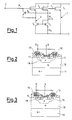
- the circuit shown in Fig. 1 consists essentially of a main branch 1 including a power MOS transistor T1 and two parallel secondary branches 2 and 3 including respective control MOS transistors T2 and T3 having the same characteristics as the power transistor and an ability to conduct a current equal to a fraction (say, one thousandth) of that of the power transistor.
- the gate and the drain of the power MOS transistor T1 are connected with the gates and with the drains of the control MOS transistors T2, T3.
- the source of transistor T2 is connected with the base of the NPN bipolar transistor T6 and, by means of resistance R3, with the collector of an NPN bipolar transistor T4.
- the emitter of transistor T4 is connected by means of a resistance R2 with the source of transistor T1 and with the emitter of an NPN bipolar transistor T5.
- the base of transistor T4 is connected directly with the corresponding collector and with the base of transistor T5.
- the collector of transistor T5 is connected with the source of transistor T3 and with the emitter of transistor T6.
- the collector of transistor T6 is connected with the gate of transistor T3 and, by means of a resistance R1, with a signal input I.
- Figure 2 shows a possible embodiment, in integrated technology, of the power MOS transistor T1, whose gate G is accomplished at strips of polysilicon 10, while the source S is accomplished at regions 11 of type N+ which are in turn obtained inside a body region 16 of type P, set on an epitaxial stratum 12 of type N, in its turn obtained on a substratum 17 of type N+, which also constitutes the drain of transistor T1.
- Figure 3 shows a possible embodiment, in vertical DMOS integrated technology, of the control MOS transistors T2, T3, whose gate G is accomplished at strips of polysilicon 13, while source S is accomplished at regions 14 of type N+ which are in turn obtained inside a body region 18 of type P set on an epitaxial stratum 15 of type N in its turn obtained on a substratum 19 of type N+ which also constitutes the drain of transistors T2, T3.
- FIGS 4, 5,6 illustrate different embodiments in integrated technology of the bipolar transistors T4, T5, T6.
- a substratum 20 of type N+ there is set an epitaxial stratum 21 of type N, on which there is obtained a body region 22 of type P which forms the base of the single transistor T4, T5, T6, whose collector is obtained in regions 23 of type N+ and whose emitter is obtained in a region 24 of type N+, regions 23 and 24 being obtained at the summit of body region 22.
- the characteristics of the single transistor T4, T5, T6 are improvable by adding a type P+ masking and by enriching region 22 during the process stage. As shown in Fig. 5, there is thus formed a further region 25 of type P+ in the proximity of the bottom of region 22.
- an embodiment in integrated technology of resistances R1, R2, R3 provides for the formation of a region 27 of type N+ accomplished with an arsenic diffusion inside a body region 28 of type P connected to ground. Such region 28 is obtained on an epitaxial stratum 29 of type N in turn superimposed on a substratum 30 of type N+.
- such resistances R1, R2, R3 may also be accomplished by means of a stratum of polysilicon 31 included in superficial oxide 32.
- a first consideration refers to the fact that the area of transistor T4 is greater than that of transistor T5, so that the current supplied by transistor T4 is normally greater than that supplied by transistor T5.
- resistance R2 has been dimensioned so as to cause across its terminals a voltage drop such as to equal the currents flowing through T4, T5 should the current supplied by transistor T2 reache a threshold value above which the triggering of the protection device is required.
- control transistors T2 and T3 are passed through by currents equal to a fraction (say, one thousandth) of that of power transistor T1 and the voltage drop across R2 is such that the current mirrored by T5 is lower than that mirrored by T4, in turn forced by T2.
- the point A the base of transistor T6, is at a voltage high.
- T3 being a current generator accomplished in the same manner as T2, attempts to supply the same current as T2 and thus the collector of T5 is at a voltage high (roughly the drain voltage of T3, T2, T1).
- T6 cannot conduct since the voltage between base and emitter is negative, since the voltage of the emitter of T6 is roughly equal to the drain voltage of transistor T1 and the voltage at the base of T6 is equal to the voltage at point A. There is thus no limitation of current.
- the current on the power MOS transistor (T1) is to be limited to 2.75A.
- T3 is one thousandth of the area of T1
- the current flowing on T2, T3 will always be equal to roughly one thousandth of that flowing on T1.
- A(T5) area of emitter T5
- A(T4) area of emitter T4
- I(T4) current of T4 collector
- I(T5) current of T5 collector
- T6 and R1 may be selected so as to ensure proper operation for a certain current at circuit input I.
- R2 is accomplished in aluminium, by means of a path similar to that which connects the different elements of the integrated circuit according to the known art, it will have a coefficient of variation with temperature equal to 4500 ppm/°c.
- R2 since a resistance accomplished with a diffusion of arsenic of type N+ has a coefficient of variation with temperature of about 1500 ppm/°C (against the 4500 ppm/°C of the aluminium resistance), R2, with the same circuit configuration of the previous case, would go from 6.54 ohms to 7.76 ohms.
Landscapes
- Semiconductor Integrated Circuits (AREA)
- Insulated Gate Type Field-Effect Transistor (AREA)
- Electronic Switches (AREA)
Abstract
Description
- The present invention relates to a device for protection against the short circuit of an MOS-type power device, with a preset dependance on the temperature at which the power device operates.
- The accomplishment of a protection against the short circuit of an MOS-type power device, integrated in the same chip and using only the technology of such power devices, is a requirement which is quite widespread in the market.
- The devices for protection against the short circuit currently available on the market depend substantially on temperature. Such a dependance limits the ability to supply current on the part of the power device, even though it may be considered useful for reasons of thermal protection.
- The object of the present invention is to accomplish a device for protection against the short circuit of an MOS-type power device, wherein the limiting current is a preset function of temperature.
- A further object is to accomplish the protection device in integrated technology together with the MOS power device without using any processing stage over in addition to those required for the accomplishment of the standard power device.
- According to the invention such object is attained with a device for protection against the short circuit of an MOS-type power device, characterized in that it comprises at least one secondary circuit branch arranged in parallel with a main circuit branch including the power transistor, said secondary branch including an MOS control transistor having the same characteristics as the power transistor under control and an ability to conduct a current equal to a fraction of that which flows through the power transistor and having its gate connected directly with that of the power transistor, said secondary branch including also means sensitive to temperature which, in the case of a current flow corresponding to the short circuit current of the power transistor, act on the gate common to the control and to the power transistors so as to lower its voltage and thus limit the conduction of same.
- The characteristics of the present invention shall be made more evident by an embodiment illustrated as a example in the enclosed drawings wherein:
- Fig. 1 illustrates a circuital accomplishment of the unit consisting of the power device and of the protection device according to the invention;
- Fig.s from 2 to 8 show possible embodiments in integrated technology of the power MOS device and of the components of the protection device.
- The circuit shown in Fig. 1 consists essentially of a main branch 1 including a power MOS transistor T1 and two parallel
secondary branches - Figure 2 shows a possible embodiment, in integrated technology, of the power MOS transistor T1, whose gate G is accomplished at strips of
polysilicon 10, while the source S is accomplished atregions 11 of type N+ which are in turn obtained inside abody region 16 of type P, set on anepitaxial stratum 12 of type N, in its turn obtained on asubstratum 17 of type N+, which also constitutes the drain of transistor T1. - Figure 3 shows a possible embodiment, in vertical DMOS integrated technology, of the control MOS transistors T2, T3, whose gate G is accomplished at strips of
polysilicon 13, while source S is accomplished atregions 14 of type N+ which are in turn obtained inside abody region 18 of type P set on anepitaxial stratum 15 of type N in its turn obtained on asubstratum 19 of type N+ which also constitutes the drain of transistors T2, T3. - Figures 4, 5,6 illustrate different embodiments in integrated technology of the bipolar transistors T4, T5, T6.
- As illustrated in Fig. 4, on a
substratum 20 of type N+ there is set anepitaxial stratum 21 of type N, on which there is obtained abody region 22 of type P which forms the base of the single transistor T4, T5, T6, whose collector is obtained inregions 23 of type N+ and whose emitter is obtained in aregion 24 of type N+,regions body region 22. - The characteristics of the single transistor T4, T5, T6 are improvable by adding a type P+ masking and by enriching
region 22 during the process stage. As shown in Fig. 5, there is thus formed afurther region 25 of type P+ in the proximity of the bottom ofregion 22. - As an alternative, with reference to Figure 6, it is possible to execute a further phosphorus masking operation with the object of creating a
further region 26 of type P- insideregion 22 of type P. - With reference to Figure 7, an embodiment in integrated technology of resistances R1, R2, R3 provides for the formation of a region 27 of type N+ accomplished with an arsenic diffusion inside a
body region 28 of type P connected to ground.Such region 28 is obtained on anepitaxial stratum 29 of type N in turn superimposed on asubstratum 30 of type N+. - With reference to Figure 8, such resistances R1, R2, R3 may also be accomplished by means of a stratum of
polysilicon 31 included insuperficial oxide 32. - From Figures 2-8 it is possible to observe that all the components of the protection device (
circuit branches - Before going on to the description of the operation of the circuit illustrated in Figure 1 it is necessary to make some considerations on the size of the components which have been introduced into the protection device.
- A first consideration refers to the fact that the area of transistor T4 is greater than that of transistor T5, so that the current supplied by transistor T4 is normally greater than that supplied by transistor T5.
- A further consideration refers to the fact that resistance R2 has been dimensioned so as to cause across its terminals a voltage drop such as to equal the currents flowing through T4, T5 should the current supplied by transistor T2 reache a threshold value above which the triggering of the protection device is required.
- With reference to Figure 1, the circuit operates as follows.
- Under normal operating conditions, control transistors T2 and T3 are passed through by currents equal to a fraction (say, one thousandth) of that of power transistor T1 and the voltage drop across R2 is such that the current mirrored by T5 is lower than that mirrored by T4, in turn forced by T2. Under these conditions the point A, the base of transistor T6, is at a voltage high. T3, being a current generator accomplished in the same manner as T2, attempts to supply the same current as T2 and thus the collector of T5 is at a voltage high (roughly the drain voltage of T3, T2, T1). Under this condition T6 cannot conduct since the voltage between base and emitter is negative, since the voltage of the emitter of T6 is roughly equal to the drain voltage of transistor T1 and the voltage at the base of T6 is equal to the voltage at point A. There is thus no limitation of current.
- Once the current of T2 has reached the threshold value above which it is required to trigger the protection device, that is in the presence of a potential short circuit condition of the power transistor T1, there is a voltage drop across the terminals of resistance R2 which gives the result of equalling the currents flowing through T4, T5. The collector of transistor T5 which is forced to conduct the same current supplied by T3, since I(T3)=I(T2) is always true, and which coincides with the emitter of T6, is lowered in voltage and, as soon as the voltage drop across R2 rises a little more, T6 enters into conduction and accomplishes the protection.
- With this circuit it is possible to accomplish a constant temperature protection (or at least with a very low variation less than 9%). It is thus seen that the mechanism triggering the protection is the difference of Vbe between T5 and T4 which, as is well known, has a positive coefficient of variation with temperature.
- If the dependance of such difference of Vbe with temperature were to be equal to the dependance of R2 with temperature, there would be a protection against short circuits which is independent of temperature, that is constant with temperature.
- Thus if a resistance is used which has a positive coefficient of variation with temperature an attempt may be made to obtain the same coefficient of variation of the difference of Vbe.
- The following are some examples of numerical accomplishments of the circuit.
- Suppose that the current on the power MOS transistor (T1) is to be limited to 2.75A.
- If is we suppose that the area of T2, T3 is one thousandth of the area of T1, the current flowing on T2, T3 will always be equal to roughly one thousandth of that flowing on T1.
- The example which follows refers to a limitation to 25°C.
- Suppose that the ratio between the areas of T4, T5 is 2/1 (this ratio may be chosen at will so that the value of resistance R2 be the most convenient).
- The difference of Vbe for this ratio (T4/T5=2) so that the currents in transistors T4 and T5 are balanced is diff.Vbe=(KT)/q x 1g[A(T5)/A(T4)] x [I(T4)/I(T5)]=18 x 10⁻³V where K = Boltzman's constant
q = electron charge
A(T5) = area of emitter T5
A(T4) = area of emitter T4
I(T4) = current of T4 collector
I(T5) = current of T5 collector
then
R2 = diff.Vbe / IL2 = 18 x 10⁻³V / 2.75 x 10⁻³V A= 6.540 ohms where IL2 is the limitation current of T2. - R3 is dimensioned so as to ensure across its terminals a voltage drop of about 100mV, so as to ensure a certain dynamic for T5, R3 = 100Mv / 2.75mA = 36.36 ohm, and it may be accomplished in polysilicon.
- The size of T6 and R1 may be selected so as to ensure proper operation for a certain current at circuit input I.
- Considering that the coefficient of variation of the difference of Vbe with temperature, with an areas ratio of 10 is 0.2mV/°C, for a ratio of 2 we will have (0.2mV x 1g2) / 1g10 = 0.06mV/°C.
- Moreover if R2 is accomplished in aluminium, by means of a path similar to that which connects the different elements of the integrated circuit according to the known art, it will have a coefficient of variation with temperature equal to 4500 ppm/°c.
- Suppose that it is required to bring the device to operate at a temperature of 150°C.
- At this temperature the difference of Vbe to balance the currents of T5 and T4 shall be 25.5mV, R2 shall be equal to 10.21, IL1 = IL2 x 1000 = 2.5mA where IL1 is T1's current of limitation.
- There is thus accomplished a variation of only 9% in the current of limitation against a variation of 125°C in temperature.
- Suppose that it is required to obtain a protection device to have a preset dependance on temperature.
- This is possible by replacing resistance R2, accomplished in the previous case in aluminium, with, say, resistances in polysilicon or resistances accomplished by the diffusion of arsenic of type N+, which, having different coefficients of thermal variation, shall ensure different dependencies on temperature.
- In particular, since a resistance accomplished with a diffusion of arsenic of type N+ has a coefficient of variation with temperature of about 1500 ppm/°C (against the 4500 ppm/°C of the aluminium resistance), R2, with the same circuit configuration of the previous case, would go from 6.54 ohms to 7.76 ohms.
- At the same time the difference of Vbe, as has already been seen, goes from 18mV to 25.5mV, again for a temperature variation from 25°C to 150°C.
- In this case IL1 = 25.5 / 7.76 = 3.28A.
- We will thus, in this case, have a current which increases with temperature.
- Similarly, if R2 is accomplished in polysilicon, since the coefficient of variation for silicon is actually negative, there will be an increase in the current of limitation as the temperature rises which is even more pronounced than in the previous case (resistance accomplished by the diffusion of arsenic of type N+).
Claims (2)
Priority Applications (5)
| Application Number | Priority Date | Filing Date | Title |
|---|---|---|---|
| EP89830500A EP0428813B1 (en) | 1989-11-17 | 1989-11-17 | Nevice for protection against the short circuit of a MOS-type power device, with a preset dependance on the temperature at which the power device operates |
| DE68921004T DE68921004T2 (en) | 1989-11-17 | 1989-11-17 | Protection device against the short circuit of a MOS power component with a predetermined dependence on the temperature at which the component operates. |
| US07/605,449 US5177659A (en) | 1989-11-17 | 1990-10-30 | Device for protection against the short circuit of an MOS-type power device, with a preset dependance on the temperature at which the power device operates |
| KR1019900017832A KR910010863A (en) | 1989-11-17 | 1990-11-02 | Short-circuit protection circuit of MOS type power supply with preset dependence on temperature at which power supply is operated |
| JP2308942A JPH03259614A (en) | 1989-11-17 | 1990-11-16 | Protection device against short circuits of MOS type power devices with preconditioning dependence on the operating temperature of the power device |
Applications Claiming Priority (1)
| Application Number | Priority Date | Filing Date | Title |
|---|---|---|---|
| EP89830500A EP0428813B1 (en) | 1989-11-17 | 1989-11-17 | Nevice for protection against the short circuit of a MOS-type power device, with a preset dependance on the temperature at which the power device operates |
Publications (2)
| Publication Number | Publication Date |
|---|---|
| EP0428813A1 true EP0428813A1 (en) | 1991-05-29 |
| EP0428813B1 EP0428813B1 (en) | 1995-02-01 |
Family
ID=8203248
Family Applications (1)
| Application Number | Title | Priority Date | Filing Date |
|---|---|---|---|
| EP89830500A Expired - Lifetime EP0428813B1 (en) | 1989-11-17 | 1989-11-17 | Nevice for protection against the short circuit of a MOS-type power device, with a preset dependance on the temperature at which the power device operates |
Country Status (5)
| Country | Link |
|---|---|
| US (1) | US5177659A (en) |
| EP (1) | EP0428813B1 (en) |
| JP (1) | JPH03259614A (en) |
| KR (1) | KR910010863A (en) |
| DE (1) | DE68921004T2 (en) |
Cited By (4)
| Publication number | Priority date | Publication date | Assignee | Title |
|---|---|---|---|---|
| WO1994010753A1 (en) * | 1992-10-28 | 1994-05-11 | Robert Bosch Gmbh | Monolithic integrated mos high-level stage component with an overload protection arrangement |
| WO1996012347A3 (en) * | 1994-10-12 | 1996-07-04 | Philips Electronics Nv | A protected switch |
| DE19640446A1 (en) * | 1996-09-30 | 1998-04-16 | Siemens Ag | Over-current protection circuit arrangement |
| EP3830870A4 (en) * | 2018-07-31 | 2021-08-25 | Texas Instruments Incorporated | POWER TRANSISTOR COUPLED WITH MULTIPLE DETECTION TRANSISTORS |
Families Citing this family (7)
| Publication number | Priority date | Publication date | Assignee | Title |
|---|---|---|---|---|
| EP0808025B1 (en) * | 1996-05-17 | 2004-11-10 | Denso Corporation | Load actuation circuit |
| JP3637848B2 (en) | 1999-09-30 | 2005-04-13 | 株式会社デンソー | Load drive circuit |
| JP4069022B2 (en) * | 2003-06-12 | 2008-03-26 | 三菱電機株式会社 | Power semiconductor device |
| US8835987B2 (en) | 2007-02-27 | 2014-09-16 | Cree, Inc. | Insulated gate bipolar transistors including current suppressing layers |
| US8193848B2 (en) * | 2009-06-02 | 2012-06-05 | Cree, Inc. | Power switching devices having controllable surge current capabilities |
| ITMI20112278A1 (en) * | 2011-12-15 | 2013-06-16 | St Microelectronics Srl | BIPOLAR POWER STRUCTURE, IN PARTICULAR FOR HIGH VOLTAGE APPLICATIONS |
| CN108512295B (en) * | 2018-04-11 | 2021-08-10 | 上海空间电源研究所 | Short-circuit prevention control method for shunt regulating circuit of spacecraft power system |
Citations (2)
| Publication number | Priority date | Publication date | Assignee | Title |
|---|---|---|---|---|
| FR2450504A1 (en) * | 1979-02-27 | 1980-09-26 | Ates Componenti Elettron | THERMAL PROTECTION DEVICE FOR A SEMICONDUCTOR ELECTRONIC COMPONENT |
| DE3821065A1 (en) * | 1987-06-22 | 1989-01-05 | Nissan Motor | MOS FIELD EFFECT TRANSISTOR DEVICE |
Family Cites Families (2)
| Publication number | Priority date | Publication date | Assignee | Title |
|---|---|---|---|---|
| US3845405A (en) * | 1973-05-24 | 1974-10-29 | Rca Corp | Composite transistor device with over current protection |
| JPS6084009A (en) * | 1983-10-14 | 1985-05-13 | Omron Tateisi Electronics Co | Protection circuit of electronic switch |
-
1989
- 1989-11-17 DE DE68921004T patent/DE68921004T2/en not_active Expired - Fee Related
- 1989-11-17 EP EP89830500A patent/EP0428813B1/en not_active Expired - Lifetime
-
1990
- 1990-10-30 US US07/605,449 patent/US5177659A/en not_active Expired - Lifetime
- 1990-11-02 KR KR1019900017832A patent/KR910010863A/en not_active Withdrawn
- 1990-11-16 JP JP2308942A patent/JPH03259614A/en active Pending
Patent Citations (2)
| Publication number | Priority date | Publication date | Assignee | Title |
|---|---|---|---|---|
| FR2450504A1 (en) * | 1979-02-27 | 1980-09-26 | Ates Componenti Elettron | THERMAL PROTECTION DEVICE FOR A SEMICONDUCTOR ELECTRONIC COMPONENT |
| DE3821065A1 (en) * | 1987-06-22 | 1989-01-05 | Nissan Motor | MOS FIELD EFFECT TRANSISTOR DEVICE |
Non-Patent Citations (1)
| Title |
|---|
| PATENT ABSTRACTS OF JAPAN vol. 9, no. 225 (E-342)(1948) 11 September 1985, & JP-A-60 84009 (TATEISHI DENKI) 13 May 1985, * |
Cited By (5)
| Publication number | Priority date | Publication date | Assignee | Title |
|---|---|---|---|---|
| WO1994010753A1 (en) * | 1992-10-28 | 1994-05-11 | Robert Bosch Gmbh | Monolithic integrated mos high-level stage component with an overload protection arrangement |
| US5523714A (en) * | 1992-10-28 | 1996-06-04 | Robert Bosch Gmbh | Monolithically integrated MOS output-stage component with overload-protection means |
| WO1996012347A3 (en) * | 1994-10-12 | 1996-07-04 | Philips Electronics Nv | A protected switch |
| DE19640446A1 (en) * | 1996-09-30 | 1998-04-16 | Siemens Ag | Over-current protection circuit arrangement |
| EP3830870A4 (en) * | 2018-07-31 | 2021-08-25 | Texas Instruments Incorporated | POWER TRANSISTOR COUPLED WITH MULTIPLE DETECTION TRANSISTORS |
Also Published As
| Publication number | Publication date |
|---|---|
| US5177659A (en) | 1993-01-05 |
| EP0428813B1 (en) | 1995-02-01 |
| DE68921004D1 (en) | 1995-03-16 |
| JPH03259614A (en) | 1991-11-19 |
| KR910010863A (en) | 1991-06-29 |
| DE68921004T2 (en) | 1995-09-21 |
Similar Documents
| Publication | Publication Date | Title |
|---|---|---|
| EP0260125A2 (en) | Electrostatic discharge protection circuit | |
| EP0428813B1 (en) | Nevice for protection against the short circuit of a MOS-type power device, with a preset dependance on the temperature at which the power device operates | |
| US5168175A (en) | Semiconductor integrated circuit using junction field effect transistor as current control element | |
| US4849654A (en) | Semiconductor integrated circuit with input protection circuit | |
| USRE37778E1 (en) | Current limiting circuit | |
| EP0802604B1 (en) | Protection circuit | |
| US4605891A (en) | Safe operating area circuit and method for an output switching device | |
| EP0424394B1 (en) | Means for reducing damage to jfets from electrostatic discharge events | |
| EP0398170A2 (en) | Timed current boost for DMOST driver with rapid turn-on and low quiescent current | |
| EP0276850A2 (en) | Semiconductor integrated circuit device with latch up preventing structure | |
| US4713599A (en) | Programmable trimmable circuit having voltage limiting | |
| EP0921619A2 (en) | A power source circuit of a semiconductor integrated circuit | |
| US4906834A (en) | Infrared detector circuit having a resistor series connected to the detector to limit the current across the pn junction of the FET | |
| JP3141865B2 (en) | Semiconductor integrated device | |
| EP0409571A2 (en) | Integrated constant current circuit with a BJT and a JFET | |
| US4701638A (en) | Antisaturation circuit for integrated PNP transistor | |
| JP2755848B2 (en) | Micro voltage detection circuit and current limiting circuit using the same | |
| JPH02226407A (en) | Power mosfet with overcurrent protecting function | |
| US20030098740A1 (en) | MOS-based voltage reference circuit | |
| JPH09138247A (en) | Overcurrent detection circuit | |
| JPH0582828A (en) | Phototransistor | |
| KR950010410B1 (en) | Low-voltage detecting circuit | |
| JP2893792B2 (en) | Power MOS transistor with overcurrent protection function | |
| JPH08102649A (en) | Power semiconductor element current detection circuit | |
| JP2855716B2 (en) | Overcurrent limiting circuit |
Legal Events
| Date | Code | Title | Description |
|---|---|---|---|
| PUAI | Public reference made under article 153(3) epc to a published international application that has entered the european phase |
Free format text: ORIGINAL CODE: 0009012 |
|
| AK | Designated contracting states |
Kind code of ref document: A1 Designated state(s): DE ES FR GB IT NL |
|
| 17P | Request for examination filed |
Effective date: 19910603 |
|
| 17Q | First examination report despatched |
Effective date: 19930809 |
|
| GRAA | (expected) grant |
Free format text: ORIGINAL CODE: 0009210 |
|
| AK | Designated contracting states |
Kind code of ref document: B1 Designated state(s): DE ES FR GB IT NL |
|
| PG25 | Lapsed in a contracting state [announced via postgrant information from national office to epo] |
Ref country code: NL Effective date: 19950201 Ref country code: ES Free format text: THE PATENT HAS BEEN ANNULLED BY A DECISION OF A NATIONAL AUTHORITY Effective date: 19950201 |
|
| ITF | It: translation for a ep patent filed | ||
| REF | Corresponds to: |
Ref document number: 68921004 Country of ref document: DE Date of ref document: 19950316 |
|
| ET | Fr: translation filed | ||
| NLV1 | Nl: lapsed or annulled due to failure to fulfill the requirements of art. 29p and 29m of the patents act | ||
| PLBE | No opposition filed within time limit |
Free format text: ORIGINAL CODE: 0009261 |
|
| STAA | Information on the status of an ep patent application or granted ep patent |
Free format text: STATUS: NO OPPOSITION FILED WITHIN TIME LIMIT |
|
| 26N | No opposition filed | ||
| REG | Reference to a national code |
Ref country code: FR Ref legal event code: D6 |
|
| PGFP | Annual fee paid to national office [announced via postgrant information from national office to epo] |
Ref country code: FR Payment date: 20011113 Year of fee payment: 13 |
|
| PGFP | Annual fee paid to national office [announced via postgrant information from national office to epo] |
Ref country code: GB Payment date: 20011121 Year of fee payment: 13 |
|
| PGFP | Annual fee paid to national office [announced via postgrant information from national office to epo] |
Ref country code: DE Payment date: 20011203 Year of fee payment: 13 |
|
| REG | Reference to a national code |
Ref country code: GB Ref legal event code: IF02 |
|
| PG25 | Lapsed in a contracting state [announced via postgrant information from national office to epo] |
Ref country code: GB Free format text: LAPSE BECAUSE OF NON-PAYMENT OF DUE FEES Effective date: 20021117 |
|
| PG25 | Lapsed in a contracting state [announced via postgrant information from national office to epo] |
Ref country code: DE Free format text: LAPSE BECAUSE OF NON-PAYMENT OF DUE FEES Effective date: 20030603 |
|
| GBPC | Gb: european patent ceased through non-payment of renewal fee | ||
| PG25 | Lapsed in a contracting state [announced via postgrant information from national office to epo] |
Ref country code: FR Free format text: LAPSE BECAUSE OF NON-PAYMENT OF DUE FEES Effective date: 20030731 |
|
| REG | Reference to a national code |
Ref country code: FR Ref legal event code: ST |
|
| PG25 | Lapsed in a contracting state [announced via postgrant information from national office to epo] |
Ref country code: IT Free format text: LAPSE BECAUSE OF NON-PAYMENT OF DUE FEES;WARNING: LAPSES OF ITALIAN PATENTS WITH EFFECTIVE DATE BEFORE 2007 MAY HAVE OCCURRED AT ANY TIME BEFORE 2007. THE CORRECT EFFECTIVE DATE MAY BE DIFFERENT FROM THE ONE RECORDED. Effective date: 20051117 |