EP3826173A1 - Power supply apparatus and method for power amplifier - Google Patents
Power supply apparatus and method for power amplifier Download PDFInfo
- Publication number
- EP3826173A1 EP3826173A1 EP19837408.4A EP19837408A EP3826173A1 EP 3826173 A1 EP3826173 A1 EP 3826173A1 EP 19837408 A EP19837408 A EP 19837408A EP 3826173 A1 EP3826173 A1 EP 3826173A1
- Authority
- EP
- European Patent Office
- Prior art keywords
- power
- circuit
- voltage
- redundant
- gate voltage
- Prior art date
- Legal status (The legal status is an assumption and is not a legal conclusion. Google has not performed a legal analysis and makes no representation as to the accuracy of the status listed.)
- Granted
Links
Images





Classifications
-
- H—ELECTRICITY
- H03—ELECTRONIC CIRCUITRY
- H03F—AMPLIFIERS
- H03F1/00—Details of amplifiers with only discharge tubes, only semiconductor devices or only unspecified devices as amplifying elements
- H03F1/52—Circuit arrangements for protecting such amplifiers
- H03F1/526—Circuit arrangements for protecting such amplifiers protecting by using redundant amplifiers
-
- H—ELECTRICITY
- H03—ELECTRONIC CIRCUITRY
- H03F—AMPLIFIERS
- H03F1/00—Details of amplifiers with only discharge tubes, only semiconductor devices or only unspecified devices as amplifying elements
- H03F1/02—Modifications of amplifiers to raise the efficiency, e.g. gliding Class A stages, use of an auxiliary oscillation
- H03F1/0205—Modifications of amplifiers to raise the efficiency, e.g. gliding Class A stages, use of an auxiliary oscillation in transistor amplifiers
- H03F1/0211—Modifications of amplifiers to raise the efficiency, e.g. gliding Class A stages, use of an auxiliary oscillation in transistor amplifiers with control of the supply voltage or current
-
- H—ELECTRICITY
- H03—ELECTRONIC CIRCUITRY
- H03F—AMPLIFIERS
- H03F1/00—Details of amplifiers with only discharge tubes, only semiconductor devices or only unspecified devices as amplifying elements
- H03F1/02—Modifications of amplifiers to raise the efficiency, e.g. gliding Class A stages, use of an auxiliary oscillation
- H03F1/0205—Modifications of amplifiers to raise the efficiency, e.g. gliding Class A stages, use of an auxiliary oscillation in transistor amplifiers
- H03F1/0211—Modifications of amplifiers to raise the efficiency, e.g. gliding Class A stages, use of an auxiliary oscillation in transistor amplifiers with control of the supply voltage or current
- H03F1/0216—Continuous control
- H03F1/0222—Continuous control by using a signal derived from the input signal
- H03F1/0227—Continuous control by using a signal derived from the input signal using supply converters
-
- H—ELECTRICITY
- H03—ELECTRONIC CIRCUITRY
- H03F—AMPLIFIERS
- H03F1/00—Details of amplifiers with only discharge tubes, only semiconductor devices or only unspecified devices as amplifying elements
- H03F1/52—Circuit arrangements for protecting such amplifiers
-
- H—ELECTRICITY
- H03—ELECTRONIC CIRCUITRY
- H03F—AMPLIFIERS
- H03F3/00—Amplifiers with only discharge tubes or only semiconductor devices as amplifying elements
- H03F3/20—Power amplifiers, e.g. Class B amplifiers, Class C amplifiers
- H03F3/21—Power amplifiers, e.g. Class B amplifiers, Class C amplifiers with semiconductor devices only
-
- H—ELECTRICITY
- H03—ELECTRONIC CIRCUITRY
- H03F—AMPLIFIERS
- H03F3/00—Amplifiers with only discharge tubes or only semiconductor devices as amplifying elements
- H03F3/20—Power amplifiers, e.g. Class B amplifiers, Class C amplifiers
- H03F3/24—Power amplifiers, e.g. Class B amplifiers, Class C amplifiers of transmitter output stages
- H03F3/245—Power amplifiers, e.g. Class B amplifiers, Class C amplifiers of transmitter output stages with semiconductor devices only
-
- H—ELECTRICITY
- H03—ELECTRONIC CIRCUITRY
- H03F—AMPLIFIERS
- H03F3/00—Amplifiers with only discharge tubes or only semiconductor devices as amplifying elements
- H03F3/68—Combinations of amplifiers, e.g. multi-channel amplifiers for stereophonics
-
- H—ELECTRICITY
- H03—ELECTRONIC CIRCUITRY
- H03F—AMPLIFIERS
- H03F3/00—Amplifiers with only discharge tubes or only semiconductor devices as amplifying elements
- H03F3/72—Gated amplifiers, i.e. amplifiers which are rendered operative or inoperative by means of a control signal
-
- H—ELECTRICITY
- H02—GENERATION; CONVERSION OR DISTRIBUTION OF ELECTRIC POWER
- H02M—APPARATUS FOR CONVERSION BETWEEN AC AND AC, BETWEEN AC AND DC, OR BETWEEN DC AND DC, AND FOR USE WITH MAINS OR SIMILAR POWER SUPPLY SYSTEMS; CONVERSION OF DC OR AC INPUT POWER INTO SURGE OUTPUT POWER; CONTROL OR REGULATION THEREOF
- H02M1/00—Details of apparatus for conversion
- H02M1/32—Means for protecting converters other than automatic disconnection
-
- H—ELECTRICITY
- H02—GENERATION; CONVERSION OR DISTRIBUTION OF ELECTRIC POWER
- H02M—APPARATUS FOR CONVERSION BETWEEN AC AND AC, BETWEEN AC AND DC, OR BETWEEN DC AND DC, AND FOR USE WITH MAINS OR SIMILAR POWER SUPPLY SYSTEMS; CONVERSION OF DC OR AC INPUT POWER INTO SURGE OUTPUT POWER; CONTROL OR REGULATION THEREOF
- H02M1/00—Details of apparatus for conversion
- H02M1/36—Means for starting or stopping converters
-
- H—ELECTRICITY
- H03—ELECTRONIC CIRCUITRY
- H03F—AMPLIFIERS
- H03F2200/00—Indexing scheme relating to amplifiers
- H03F2200/451—Indexing scheme relating to amplifiers the amplifier being a radio frequency amplifier
-
- H—ELECTRICITY
- H03—ELECTRONIC CIRCUITRY
- H03F—AMPLIFIERS
- H03F2200/00—Indexing scheme relating to amplifiers
- H03F2200/516—Some amplifier stages of an amplifier use supply voltages of different value
-
- H—ELECTRICITY
- H03—ELECTRONIC CIRCUITRY
- H03F—AMPLIFIERS
- H03F2203/00—Indexing scheme relating to amplifiers with only discharge tubes or only semiconductor devices as amplifying elements covered by H03F3/00
- H03F2203/72—Indexing scheme relating to gated amplifiers, i.e. amplifiers which are rendered operative or inoperative by means of a control signal
- H03F2203/7206—Indexing scheme relating to gated amplifiers, i.e. amplifiers which are rendered operative or inoperative by means of a control signal the gated amplifier being switched on or off by a switch in the bias circuit of the amplifier controlling a bias voltage in the amplifier
Definitions
- the present application relates to, but is not limited to, the field of base station communication, in particular to a power supply apparatus and method for a power amplifier.
- GaN gallium nitride
- the GaN power amplifier has strict power-on and power-off timing requirements, i.e., a gate voltage must be powered on earlier than a drain voltage and powered off later than the drain voltage. If the power supply of the GaN power amplifier does not satisfy the power-on and power-off timing requirements, the power-on or power-off is in a short-circuit state, such that the GaN power amplifier is easily burnt. Due to high cost of the GaN power amplifier, a lot of loss in cost will be caused if the GaN power amplifier is burnt.
- Embodiments of the present application provide a power supply apparatus and method for a power amplifier, which at least achieve the reliability in power supply timing of a power amplifier in a base station.
- a power supply apparatus for a power amplifier includes a first power circuit, a second power circuit, a gate voltage circuit, an enable circuit, a redundant circuit, a power-off holding circuit and a detection and control circuit, where the redundant circuit is connected to the first power circuit, the second power circuit, the power-off holding circuit and the gate voltage circuit, and configured to supply an input voltage to the power-off holding circuit after performing redundancy on an output voltage of the first power circuit and an output voltage of the second power circuit, and to supply an input voltage to the gate voltage circuit after performing redundancy on the output voltage of the first power circuit and an output voltage of the power-off holding circuit; the power-off holding circuit is connected to the gate voltage circuit, and configured to provide power-off energy holding and power-off delay to a gate voltage output by the gate voltage circuit; and the detection and control circuit is connected to the power-off holding circuit, the gate voltage circuit and the enable circuit, and configured to inspect the power-off holding circuit during a power-on process, to detect a voltage of
- a power supply method for a power amplifier includes: generating, by a redundant circuit, a first redundant backup voltage after performing redundancy on an output voltage of a first power circuit and an output voltage of a second power circuit, to supply an input voltage to a power-off holding circuit; generating, by the redundant circuit, a second redundant backup voltage after performing redundancy on the output voltage of the first power circuit and an output voltage of the power-off holding circuit, to supply an input voltage to the gate voltage circuit; and inspecting, by a detection and control circuit, the power-off holding circuit during a power-on process; detecting a voltage of the power-off holding circuit and a voltage of the gate voltage circuit during a normal operation and a power-off process; and realizing, by enable control of an enable circuit, where a detection result satisfies a judgment condition, that power-on of the gate voltage output by the gate voltage circuit is earlier than power-on of a drain voltage output by the second power circuit and power-off of the gate voltage output by
- the terms “include”, “contain” or any other variation thereof, are intended to encompass a non-exclusive inclusion, such that a method or apparatus comprising a series of elements includes not only the elements expressly recited, but also other elements not expressly listed, or elements inherent to the method or apparatus being practiced.
- the method or apparatus comprising the element is not excluding but may have additional relevant elements (e.g., a step in the method or unit in the apparatus, e.g., the unit may be part of a circuit, part of a processor, part of a program or software, etc.).
- the power supply method for a power amplifier provided in the embodiments of the present application includes a series of steps.
- the power supply method for a power amplifier provided in the embodiments of the present application is not limited to the described steps.
- the power supply apparatus for a power amplifier provided in the embodiments of the present application includes a series of components, but the power supply apparatus for a power amplifier provided in the embodiments of the present application is not limited to the explicitly described components.
- first ⁇ second in the embodiments of the present application is merely a distinction between similar objects and does not represent a particular order of objects.
- first ⁇ second may interchange a particular order or order of precedence, if allowed.
- Objects distinguished by the term “first ⁇ second” may be interchangeable where appropriate to enable embodiments of the present application to be implemented in order other than the order illustrated or described herein.
- FIG. 1 An application scenario of a power supply method for a power amplifier of the present application is shown in FIG. 1 , including: a base station 101 and a base station 102. There are three terminals, namely a terminal 11, a terminal 12, and a terminal 13 in a cell coverage area of the base station 101. There are five terminals, namely, a terminal 21, a terminal 22, a terminal 23, a terminal 24, and a terminal 25 in a cell coverage area of the base station 102. Each terminal may be a mobile phone terminal as shown in FIG. 1 , or may be one or more Internet of Things (IoT) terminals.
- a network element device e.g., a base station
- a network element device has strict power-on and power-off timing requirements on a GaN power amplifier, i.e., a gate voltage must be powered on earlier than a drain voltage and powered off later than the drain voltage.
- the first scheme is realized by an electronic switch circuit
- the second scheme is realized by a discharge circuit
- the third scheme is realized by a dedicated timing control chip or a single chip microcomputer or a controller.
- the electronic switch circuit before a drain voltage is supplied to the power amplifier, the electronic switch circuit is controlled by a gate voltage, and an electronic switch cannot be turned on until the gate voltage is established. The electronic switch is turned off immediately once the gate voltage is powered off.
- the first scheme has many problems in terms of the reliability.
- the power supply in a previous stage will be restarted after being turned off, which easily exceeds a safe operating area (SOA) curve of the electronic switch and damages the electronic switch. Therefore, the reliability is mediocre.
- SOA safe operating area
- the reliability in supplying power is achieved by discharging the drain voltage.
- a reference voltage comparison point of the discharge circuit is susceptible to interference and abnormalities, which easily causes high-voltage discharge and results in damage to the electronic switch of the discharge circuit. Therefore, the reliability is mediocre.
- the timing cannot be under controlled when the controller is abnormal. Therefore, the reliability in supplying power cannot be guaranteed and there are limitations.
- a power supply apparatus for a power amplifier includes a gate voltage circuit, an enable circuit, a redundant circuit, a power-off holding circuit and a detection and control circuit.
- the redundant circuit is connected to a first power circuit, a second power circuit, the power-off holding circuit and the gate voltage circuit, and configured to supply an input voltage to the power-off holding circuit after performing redundancy on an output voltage of the first power circuit and an output voltage of the second power circuit, and to supply an input voltage to the gate voltage circuit after performing redundancy on the output voltage of the first power circuit and an output voltage of the power-off holding circuit.
- the power-off holding circuit is connected to the gate voltage circuit, and configured to provide power-off energy holding and power-off delay to a gate voltage output by the gate voltage circuit.
- the detection and control circuit is connected to the power-off holding circuit, the gate voltage circuit and the enable circuit, and configured to inspect the power-off holding circuit during a power-on process, to detect a voltage of the power-off holding circuit and a voltage of the gate voltage circuit during a power-off process, and to realize, where a detection result satisfies a judgment condition, by means of enable control of the enable circuit, that power-on of the gate voltage is earlier than power-on of a drain voltage output by the second power circuit, and that power-off of the gate voltage is later than power-off of the drain voltage output by the second power circuit.
- the power-off holding circuit and the gate voltage circuit can be continuously powered by the energy that can be stored redundantly and by using the redundant circuit, signals can be subjected to enable control based on a detection result during the power-on and power-off processes, such that power-on of the gate voltage is earlier than power-on of the drain voltage output by the second power circuit and power-off of the gate voltage is later than power-off of the drain voltage output by the second power circuit, thereby ensuring power-on holding and power-off delay and thus realizing the reliability in power supply timing of the power amplifier.
- the power supply apparatus 310 for the power amplifier includes a first power circuit 311, a second power circuit 312, a redundant circuit 313, a power-off holding circuit 314, a gate voltage circuit 315, a detection and control circuit 316, and an enable circuit 317.
- the redundant circuit 313 is configured to supply an input voltage to the power-off holding circuit 314 after performing redundancy an output voltage of the first power circuit (a 1 st power circuit) 311 and an output voltage of the second power circuit (a P1 st power circuit) 312.
- the first power circuit (the 1 st power circuit) 311 supplies power to a digital load of a base station.
- the second power circuit (the P1 st power circuit) 312 supplies power to a drain of a power amplifier.
- the redundant circuit 313 is further configured to supply an input voltage to the gate voltage circuit 315 after performing redundancy on the output voltage of the first power circuit (the 1 st power circuit) 311 and an output voltage of the power-off holding circuit 314.
- the power-off holding circuit 314 is configured to provide power-off energy holding and power-off delay to a gate voltage output by the gate voltage circuit.
- the gate voltage circuit is configured to generate a gate voltage for the power amplifier and to supply power to a gate of the power amplifier.
- the detection and control circuit 316 is configured to inspect the power-off holding circuit during the power-on process, such that the reliability of the power-off process can be ensured at the beginning of the power-on process.
- the detection and control circuit 316 is also configured to detect (may be configured to detect in real time) a voltage of the power-off holding circuit 314 and a voltage of the gate voltage circuit 315 during a normal operation and a power-off process; and, to output, where a detection result satisfies a judgment condition, an output signal to the enable circuit by means of the enable control of the enable circuit 317 (i.e., after logical judgment processing of the detection result and the judgment condition), so as to control the enable circuit to realize that power-on of the gate voltage is earlier than power-on of a drain voltage output by the second power circuit and power-off of the gate voltage is later than power-off of the drain voltage output by the second power circuit.
- the energy redundancy conversion of one or more drain voltages of the power amplifier is fully utilized during the power-off process, to fully delay the power-off holding circuit, thereby ensuring that the power-off of the gate voltage is later than power-off of the drain voltage.
- the first power circuit (such as the 1 st power circuit) is powered on to supply power to the digital load of the base station.
- the redundancy is performed on the output voltage of the first power circuit (such as the 1 st power circuit) and the output voltage of the second power circuit (such as the P1 st power circuit) to supply power to the power-off holding circuit, and meanwhile the redundancy is performed on the output voltage of the power-off holding circuit and the output voltage of the first power circuit (such as the 1 st power circuit) to supply power to the gate voltage circuit.
- the output voltage of the second power circuit (such as the P1 st power circuit) can be subjected to enable control, thereby realizing that power-on of the gate voltage output by the gate voltage circuit is earlier than power-on of the drain voltage output by the second power circuit (such as the P1 st power circuit).
- the gate voltage is generated by the redundant circuit (in one embodiment, by a redundant backup circuit) to enable the drain of the power amplifier to be turned on. A gate voltage is generated redundantly again after the drain voltage is powered on.
- the detection and control circuit is configured to inspect the power-off holding circuit during the power-on process, such that the reliability of the power-off process can be ensured at the beginning of the power-on process.
- the energy redundancy conversion of one or more drain voltages of the power amplifier is fully utilized during the power-off process, to fully delay the power-off holding circuit, thereby ensuring that the power-off of the gate voltage is later than power-off of the drain voltage. Since power-off energy holding and power-off delay are achieved, the power-off of the gate voltage is later than power-off of the drain voltage, thereby solving the problem in terms of the reliability in power supply timing of the power amplifier.
- the present application can reliably and effectively guarantee the power supply requirements of the GaN power amplifier no matter any power channel fails, or any power channel is powered on or off before or after other power channels, or an abnormal situation occurs during the normal operation.
- the redundancy refers to the realization of "OR" power supply of a plurality of voltages, that is, selectively supplying power, where the plurality of voltages does not affect each other, and the normal operation of the system can be guaranteed as long as at least one of the voltages is normal.
- the power supply apparatus for the power amplifier according to the embodiment of the present application is more compact and reliable, can be widely used in a wireless communication base station device of the 4th Generation mobile communication system (4G) or the 5th generation mobile communication system (5G), is highly versatile and has a wide range of application values.
- the redundant circuit includes a first redundant circuit (a redundant circuit 1) and a second redundant circuit (a redundant circuit 2).
- a first input terminal of the first redundant circuit (the redundant circuit 1) is connected to an output terminal of the first power circuit (the 1 st power circuit).
- a second input terminal of the first redundant circuit (the redundant circuit 1) is connected to an output terminal of the second power circuit (the P1 st power circuit).
- An output terminal of the first redundant circuit (the redundant circuit 1) is connected to an input terminal of the power-off holding circuit, and configured to supply an input voltage to the power-off holding circuit.
- the first power circuit (the 1 st power circuit) supplies power to a digital load of a base station.
- the second power circuit (the P1 st power circuit) supplies power to a drain of the power amplifier.
- the redundant circuit further includes the second redundant circuit (a redundant circuit 2).
- a first input terminal of the second redundant circuit (the redundant circuit 2) is connected to an output terminal of the first power circuit (the 1 st power circuit).
- a second input terminal of the second redundant circuit (the redundant circuit 2) is connected to an output terminal of the power-off holding circuit.
- An output terminal of the second redundant circuit (the redundant circuit 2) is connected to the gate voltage circuit (a 1 st gate voltage circuit), and configured to supply an input voltage to the gate voltage circuit.
- the gate voltage circuit is configured to generate a gate voltage for the power amplifier and to supply power to a gate of the power amplifier.
- a first input terminal of the detection and control circuit is connected to the output terminal of the power-off holding circuit; a second input terminal of the detection and control circuit is connected to an output terminal of the gate voltage circuit; and an output terminal of the detection and control circuit is connected to an input terminal of the enable circuit.
- an output terminal of the enable circuit is connected to an enable control circuit of the second power circuit (the P1 st power circuit), and configured to perform start control on the second power circuit (the P1 st power circuit).
- the power supply apparatus for the power amplifier may include a 1 st power circuit, a P1 st power circuit, a redundant circuit 1, a power-off holding circuit 2, a redundant circuit 2, a gate voltage circuit, a detection and control circuit and an enable circuit.
- the 1 st power circuit supplies power to the digital load of the base station; and the P1 st power circuit supplies power to a drain of a GaN power amplifier.
- the power-off holding circuit is configured to provide power-off energy holding and power-off delay to a gate voltage output by the gate voltage circuit, where an input terminal of the power-off holding circuit is connected to an output terminal of the redundant circuit 1, and an output terminal of the power-off holding circuit is connected to an input terminal of the redundant circuit 2.
- the redundant circuit 2 is configured to provide power-off energy holding and power-off delay to a gate voltage, where one input terminal of the redundant circuit 2 is connected to an output terminal of the 1 st power circuit, the other input terminal of the redundant circuit 2 is connected to the output terminal of the power-off holding circuit, and an output terminal of the redundant circuit 2 is connected to an input terminal of a 1 st gate voltage circuit.
- the gate voltage circuit is configured to generate a gate voltage for the GaN power amplifier and to supply power to a gate of a P1 st GaN power amplifier.
- One input terminal of the detection and control circuit is connected to the output terminal of the power-off holding circuit; and the other input terminal of the detection and control circuit is connected to the output terminal of the gate voltage circuit.
- an output signal of the detection and control circuit controls the enable circuit.
- the enable circuit is configured to control the start of the P1 st power circuit, where an input terminal of the enable circuit is connected to the output terminal of the detection and control circuit, and an output terminal of the enable circuit is connected to an enable control circuit of the P1 st power circuit.
- the first power circuit (the 1 st power circuit) includes one power supply or multiple power supplies.
- the power supplied by the 1 st power circuit to a load of a digital part may not be limited to one power supply, but may be 1 st to m th power supplies.
- the second power circuit (the P1 st power circuit) includes one power supply or multiple power supplies.
- the power supplied by the P1 st power circuit to the power amplifier may not be limited to one power supply, but can be the P1 st to Pn th power supplies.
- an input source of the first power circuit (the 1 st power circuit) is the same as that of the second power circuit (the P1 st power circuit); or an input source of the first power circuit (the 1 st power circuit) is different from that of the second power circuit (the P1 st power circuit).
- the input sources of 1 st to m th power supplies and of P1 st to Pn th power supplies can be the same or different.
- the first power circuit (the 1 st power circuit) and the second power circuit (the P1 st power circuit) both connected to the first redundant circuit (the redundant circuit 1) is a combination of at least one from a plurality of power supplies.
- the first power circuit connected to the redundant circuit 1 may be one, several or all of the 1 st to m th power supplies, and one, several or all of the P1 st to Pn th power supplies.
- the redundant circuit 1 can be implemented as an electronic switch, a diode, a relay, a switch circuit or the like.
- the first power circuit (the 1 st power circuit) connected to the second redundant circuit (the redundant circuit 2) includes one power supply or at least one from a plurality of power supplies.
- the first power circuit connected to the redundant circuit 2 may be one, several or all of the 1 st to m th power supplies.
- the redundant circuit 2 is configured to perform redundancy on the output voltage of the first power circuit and the output voltage of the power-off holding circuit, and supply energy to the gate voltage circuit.
- the implementation form of the power-off holding circuit includes: a boost circuit of a wide input range, a step-down circuit of a wide input range, other conversion energy storage circuit or an energy storage element.
- the implementation form of the gate voltage circuit includes: one or more of a plurality of power amplifiers.
- one or more of the 1 st to n th power amplifiers supply a gate voltage
- the implementation form of the gate voltage circuit can be flexibly configured according to load power of the gate voltage.
- the present embodiment further provides a power supply method for a power amplifier. This method is implemented based on the above-mentioned power supply apparatus for the power amplifier, which will not be repeated because it has been described in the present application.
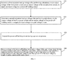
- a power supply method for the power amplifier includes steps 410-440.
- a first redundant backup voltage is generated after performing redundancy on an output voltage of the first power circuit and an output voltage of the second power circuit, to supply an input voltage to the power-off holding circuit.
- a first redundant backup voltage is generated after performing redundancy on an output voltage of the 1 st power circuit and an output voltage of the P1 st power circuit, to supply an input voltage to the power-off holding circuit.
- a second redundant backup voltage is generated after performing redundancy on the output voltage of the first power circuit and an output voltage of the power-off holding circuit, to supply an input voltage to the gate voltage circuit.
- a second redundant backup voltage is generated after performing redundancy on the output voltage of the 1 st power circuit and the output voltage of the power-off holding circuit, to supply an input voltage to the gate voltage circuit.
- the power-off holding circuit is inspected during the power-on process.
- a voltage of the power-off holding circuit and a voltage of the gate voltage circuit are detected during a normal operation and a power-off process, to realize, where a detection result satisfies a judgment condition, that power-on of a gate voltage is earlier than power-on of a drain voltage and power-off of the gate voltage is later than power-off of the drain voltage, by means of enable control.
- the gate voltage is output by the gate voltage circuit, and the drain voltage is output by the second power circuit.
- the output voltage of the power-off holding circuit and the output voltage of the gate voltage circuit are detected (may be detected in real time) during the normal operation and the power-off process.
- the first redundant backup voltage is stored in the first redundant circuit (the redundant circuit 1)
- the second redundant backup voltage is stored in the second redundant circuit (the redundant circuit 2).
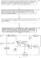
- the method includes the following steps 510-540.
- a first redundant backup voltage is generated after performing redundancy on an output voltage of the first power circuit and an output voltage of the second power circuit, and an input voltage is supplied to the power-off holding circuit through the first redundant circuit (the redundant circuit 1).
- a first redundant backup voltage is generated after performing redundancy on an output voltage of the 1 st power circuit and an output voltage of the P1 st power circuit, as an input voltage supplied to the power-off holding circuit.
- a second redundant backup voltage is generated after performing redundancy on the output voltage of the first power circuit and an output voltage of the power-off holding circuit, and an input voltage is supplied to the gate voltage circuit through the second redundant circuit (the redundant circuit 2).
- a second redundant backup voltage is generated after performing redundancy on the output voltage of the 1 st power circuit and the output voltage of the power-off holding circuit, as an input voltage supplied to the gate voltage circuit.
- the power-off holding circuit is inspected during the power-on process.
- the enable circuit is controlled to be valid to enable the second power circuit (the P1 st power circuit) to be powered on.
- a drain of the power amplifier is enabled to be turned on.
- the first redundant backup voltage is stored in the first redundant circuit (the redundant circuit 1)
- the second redundant backup voltage is stored in the second redundant circuit (the redundant circuit 2).
- the method includes the following steps 610-640.
- a first redundant backup voltage is generated after performing redundancy on an output voltage of the first power circuit and an output voltage of the second power circuit, and the power-off holding circuit is continued to be supplied with power through the first redundant circuit (the redundant circuit 1).
- a first redundant backup voltage is generated after performing redundancy on an output voltage of the 1 st power circuit and an output voltage of the P1 st power circuit, to continue to supply power to the power-off holding circuit.
- a second redundant backup voltage is generated after performing redundancy on the output voltage of the first power circuit and an output voltage of the power-off holding circuit, and the gate voltage circuit is powered on through the second redundant circuit (the redundant circuit 2), so as to continue to supply power to a gate of the power amplifier.
- a second redundant backup voltage is generated after performing redundancy on the output voltage of the 1 st power circuit and the output voltage of the power-off holding circuit, to continue to supply power to the gate voltage circuit.
- a voltage of the power-off holding circuit and a voltage of the gate voltage circuit are detected during the power-off process.
- a detection is performed to judge whether the gate voltage is higher than a safe voltage of the power amplifier, and in response to a judgment result of a detection that the gate voltage is higher than the safe voltage of the power amplifier, the gate voltage circuit is subsequently powered off.
- the power supplied to the gate voltage circuit is maintained for a specified time by the second redundant circuit (the redundant circuit 2) in response to the judgment result of the detection that the gate voltage is higher than the safe voltage of the power amplifier; and the gate voltage circuit is powered off in response to a judgment result that the output voltage of the gate voltage circuit is lower than an undervoltage point of the gate voltage circuit.
- the 1 st power circuit is powered on to supply power to the digital load of the base station.
- the redundancy is performed on the output voltage of the 1 st power circuit and the output voltage of the P1 st power circuit to supply power to the power-off holding circuit, and meanwhile the redundancy is performed on the output voltage of the power-off holding circuit and the output voltage of the 1 st power circuit to supply power to the gate voltage circuit.
- the output voltage of the P1 st power circuit can be subjected to enable control, thereby realizing that power-on of a gate voltage output by the gate voltage circuit is earlier than power-on of a drain voltage output by the P1 st power circuit. That is, the energy stored in a drain voltage power circuit of the P1 st power circuit is sufficiently utilized and subjected to redundancy to generate the first redundant backup voltage, which is then supplied to the power-off holding circuit, thereby providing a stable power-off holding circuit.
- the first redundant backup voltage which is generated by performing redundancy on the 1 st power circuit and the power-off holding circuit again is supplied to the gate voltage circuit, thereby providing a reliable gate voltage circuit and ensure the reliability in power-off delay under any conditions.
- the power-on process is not affected by the input voltage of the 1 st power circuit and the input voltage of the P1 st power circuit, and has no mandatory requirement on a power-on sequence for the 1 st power circuit and the P1 st power circuit.
- the redundant circuit and the detection and control circuit ensure that the P1 st power circuit is enabled if the output voltage of the gate voltage circuit is normal, which reliably realizes the normal power-on requirements of the GaN power amplifier. Meanwhile, the power-off holding circuit is inspected during the power-on process, and the output of the P1 st power circuit cannot be started if an abnormality is identified.
- the power-off holding circuit is inspected at the instant of power-on, which ensures that the power-on and power-off timing is more reliable.
- the P1 st to Pn th power circuits are powered off when input sources of the P1 st to Pn th power circuits are powered off.
- the power-off holding circuit can ensure that the drain voltage of the GaN power amplifier falls within a safe voltage area of the SOA curve, and then sufficient delay of 1 st to n th gate voltage circuits in lower input ensures that the gate voltage is powered off at last.
- the redundant circuit, the power-off holding circuit and the gate voltage circuit will not lose power, thereby ensuring the reliability in supplying power.
- the power supplies of the P1 st to Pn th power circuits do not affect each other, and are applicable to a power amplifier of a multi-channel base station, thereby ensuring the reliability in supplying power.
- the power supply apparatus for a power amplifier may be implemented by software, and the software (such as a computer program) may be stored in a memory, which may be a volatile memory or a non-volatile memory, or may include both a volatile memory and a non-volatile memory.
- the non-volatile memory may be a read only memory (ROM), a programmable read only memory (PROM), an erasable programmable read only memory (EPROM), an electrically erasable programmable read only memory (EEPROM), a ferromagnetic random access memory (FRAM), a flash memory, a magnetic surface memory, an optical disc, or a compact disc read only memory (CD-ROM).
- the magnetic surface storage may be a magnetic disk storage or a magnetic tape storage.
- the volatile memory may be a random access memory (RAM) that functions as an external cache.
- RAM random access memory
- many forms of RAM may be used, such as static random access memory (SRAM), synchronous static random access memory (SSRAM), dynamic random access memory (DRAM), synchronous dynamic random access memory (SDRAM), double data rate synchronous dynamic random access memory (DDRSDRAM), enhanced synchronous dynamic random access memory (ESDRAM), syncLink dynamic random access memory (SLDRAM), direct rambus random access memory (DRRAM).
- SRAM static random access memory
- SSRAM synchronous static random access memory
- DRAM dynamic random access memory
- SDRAM synchronous dynamic random access memory
- DDRSDRAM double data rate synchronous dynamic random access memory
- ESDRAM enhanced synchronous dynamic random access memory
- SLDRAM syncLink dynamic random access memory
- DRRAM direct rambus random access memory
- An embodiment of the present application provides a computer-readable storage medium, configured to store a calculation program provided in the above embodiments, in order to complete the steps of the above methods.
- the computer-readable storage medium may be a memory such as FRAM, ROM, PROM, EPROM, EEPROM, Flash Memory, magnetic surface memory, optical disk, or CD-ROM; also may be one or more devices including one or any combination of the above memories.
- the enable circuit in the embodiments of the present application may be a generating circuit of an x th power supply, or any electronic switching circuit before and after a Px power supply, which is not limited to the description of the enable circuit in the following embodiments.
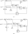
- FIG. 6 is a schematic structural diagram of a power supply apparatus for a power amplifier provided by an embodiment of the present application.
- a 1 st power circuit supplies power to a digital load of a base station
- a P1 st power circuit supplies power to a power amplifier.
- An output voltage of the 1 st power circuit and an output voltage of the P1 st power circuit supply power to a power-off holding circuit through a redundant circuit 1, and an output voltage of the power-off holding circuit and the output voltage of the 1 st power circuit supply power to a gate voltage circuit through a redundant circuit 2.
- the output voltage of the P1 st power circuit supplies power to the power amplifier by means of enable control.
- FIG. 7 is a schematic structural diagram of another power supply apparatus for the power amplifier provided by an embodiment of the present application.
- This schematic diagram is the same as FIG. 6 except that an input voltage of a redundant circuit 1 is optional, which may be an input voltage of a 1 st power circuit or an output voltage of the 1 st power circuit.
- the 1 st power circuit supplies power to a digital load of a base station, and a P1 st power circuit supplies power to a power amplifier.
- An input voltage of the 1 st power circuit and an output voltage of the P1 st power circuit supply power to a power-off holding circuit through the redundant circuit 1; or an output voltage of the 1 st power circuit and the output voltage of the P1 st power circuit supply power to the power-off holding circuit through the redundant circuit 1.
- An output voltage of the power-off holding circuit and the output voltage of the 1 st power circuit supply power to a gate voltage circuit through a redundant circuit 2.
- FIG. 8 is a schematic structural diagram of yet another power supply apparatus for the power amplifier provided by an embodiment of the present application.
- the content shown in FIG. 8 is the same as that described in FIG. 6 except that an enable circuit can enable an electronic switch in front of a P1 st power circuit.
- a 1 st power circuit supplies power to a digital load of a base station
- the P1 st power circuit supplies power to a power amplifier.
- An output voltage of the 1 st power circuit and an output voltage of the P1 st power circuit supply power to a power-off holding circuit through a redundant circuit 1, and an output voltage of the power-off holding circuit and the output voltage of the 1 st power circuit supply power to a gate voltage circuit through a redundant circuit 2.
- the output voltage of the P1 st power circuit supplies power to the power amplifier by means of enable control.
- the enable circuit is connected to the P1 st power circuit through an electronic switch, an input terminal of the P1 st power circuit is connected to an output terminal of the electronic switch, and the enable circuit can enable the electronic switch in front of the P1 st power circuit.
- FIG. 9 is a schematic structural diagram of still another power supply apparatus for a power amplifier provided by an embodiment of the present application.
- the content shown in FIG. 9 is consistent with that described in FIG. 6 except that an enable circuit can enable an electronic switch behind a P1 st power circuit.
- a 1 st power circuit supplies power to a digital load of a base station
- the P1 st power circuit supplies power to a power amplifier.
- An output voltage of the 1 st power circuit and an output voltage of the P1 st power circuit supply power to a power-off holding circuit through a redundant circuit 1, and an output voltage of the power-off holding circuit and the output voltage of the 1 st power circuit supply power to a gate voltage circuit through f a redundant circuit 2.
- the output voltage of the P1 st power circuit supplies power to the power amplifier by means of enable control.
- the enable circuit is connected to the P1 st power circuit through an electronic switch, an input terminal of the P1 st power circuit is connected to an input terminal of the electronic switch, and the enable circuit can enable the electronic switch behind the P1 st power circuit.
- FIG. 10 is a schematic structural diagram of still another power supply apparatus for the power amplifier provided by an embodiment of the present application.
- the content shown in FIG. 10 is consistent with that described in FIG. 7 except that the inputs of a redundant circuit 1 in this schematic diagram are output voltages of 1 5t , 2 nd , ..., m th power circuits and an output voltage of a P1 st power circuit; the inputs of a redundant circuit 2 in this schematic diagram are output voltages of 1 st , 2 nd , ..., m th power circuits and an output voltage of a power-off holding circuit; and the output of the redundant circuit 2 in this schematic diagram generates input voltages of 1 st , 2 nd , ..., n th gate voltage circuits..
- the 1 st , 2 nd , ..., m th power circuits supply power a digital load of a base station, and the P1 st power circuit supplies power to the power amplifier.
- the output voltages of the 1 st , 2 nd , ..., m th power circuits and the output voltage of the P1 st power circuit supply power to the power-off holding circuit through a redundant circuit 1; and the output voltage of the power-off holding circuit and the output voltages of the 1 st , 2 nd , ..., m th power circuits supply power to a gate voltage circuit through a redundant circuit 2; and an output of the redundant circuit 2 generates input voltages of 1 st , 2 nd , ..., m th gate voltage circuits.
- the output voltage of the P1 st power circuit supplies power to a power amplifier by means of enable control.
- FIG. 11 is a schematic structural diagram of still another power supply apparatus for the power amplifier provided by an embodiment of the present application.
- the content shown in FIG. 11 is consistent with that described in FIG. 7 except that the inputs of a redundant circuit 1 in this schematic diagram are output voltages of 1 5t , 2 nd , ..., m th power circuits and output voltages of P1 st , P2 nd , ..., Pn th power circuits; the inputs of a redundant circuit 2 in this schematic diagram are output voltages of 1 st , 2 nd , ..., m th power circuits and an output voltage of a power-off holding circuit; and the output of the redundant circuit 2 in this schematic diagram generates input voltages of 1 st , 2 nd , ..., n th gate voltage circuits.
- the 1 st , 2 nd , ..., m th power circuits supply power a digital load of a base station
- the P1 st , P2 nd , ..., Pn th power circuits supply power to the power amplifier.
- the output voltages of the 1 st , 2 nd , ..., m th power circuits and the output voltages of the P1 st , P2 nd , ..., Pn th power circuits supply power to the power-off holding circuit through a redundant circuit 1; and the output voltage of the power-off holding circuit and the output voltages of the 1 st , 2 nd , ..., m th power circuits supply power to a gate voltage circuit through a redundant circuit 2; and the output of the redundant circuit 2 generates input voltages of 1 st , 2 nd , ..., m th gate voltage circuits.
- the output voltage of the P1 st power circuit supplies power to a power amplifier by means of enable control.
- FIG. 12 is a schematic structural diagram of still another power supply apparatus for the power amplifier provided by an embodiment of the present application.
- the content shown in FIG. 12 is consistent with that described in FIG. 11 except that the output of a redundant circuit 2 generates a gate voltage through an n th gate voltage circuit.
- 1 st , 2 nd , ..., m th power circuits supply power to a digital load of a base station
- P1 st , P2 nd , ..., Pn th power circuits supply power to the power amplifier.
- Output voltages of the 1 st , 2 nd , ..., m th power circuits and output voltages of the P1 st, P2 nd , ..., Pn th power circuit supply power to a power-off holding circuit through a redundant circuit 1; and an output voltage of the power-off holding circuit and the outputs of the 1 st , 2 nd , ..., m th power circuits supply power to a gate voltage circuit through a redundant circuit 2; and the output of the redundant circuit 2 generates an input voltage of an n th gate voltage circuit.
- the output voltage of the P1 st power circuit supplies power to a power amplifier by means of enable control.
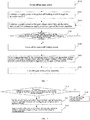
- FIG. 13 is a flowchart of power-on control in a power supply apparatus for a power amplifier provided by an embodiment of the present application, which includes the following steps 1010-1070.
- an input source is powered on; and a 1 st power circuit is powered on.
- a power-off holding circuit is powered on through a redundant circuit 1.
- a gate voltage circuit is powered on through a redundant circuit 2.
- a detection and control circuit inspects whether an output voltage of the power-off holding circuit and an output voltage of the gate voltage circuit are normal; step 1070 is performed in response to a judgment result that any one of the output voltage of the power-off holding circuit and the output voltage of the gate voltage circuit is abnormal; and step 1050 is performed in response to a judgment result that both the output voltage of the power-off holding circuit and the output voltage of the gate voltage circuit are normal.
- an enable circuit is valid and enables a P1 st power circuit to be powered on.
- a gate of the power amplifier is powered on.
- step 1070 power-off for maintenance and check is performed and step 1010 returns to be performed.
- FIG. 14 is a flowchart of power-off control in a power supply apparatus for a power amplifier provided by an embodiment of the present application, which includes the following steps 2010-2070.
- a power-off holding circuit is continued to be supplied with power through a redundant circuit 1.
- a gate voltage circuit is continued to be supplied with power through a redundant circuit 2 to continue to supply power to a gate of the power amplifier.
- step 2040 power-off holding is performed, and a detection and control circuit inspects whether a gate voltage is lower than an SOA safe voltage; the step 2030 proceeds in response to a judgment result that the gate voltage is higher than the SOA safe voltage of the power amplifier; and step 2050 proceeds in response to a judgment result that the gate voltage is lower than the SOA safe voltage of the power amplifier.
- the power-off holding circuit is powered off.
- step 2060 after being maintained by the redundant circuit 2 for a certain period of time, the output voltage of a gate voltage circuit is lower than an undervoltage point of the gate voltage circuit, and the gate voltage circuit is then powered off.
- a gate of the power amplifier is turned off.
- FIG. 15 is a control flowchart showing that the output of a Pn th power circuit is abnormal when a power supply apparatus for a power amplifier provided by an embodiment of the present application operates normally, that is, when any one of the power amplifiers is abnormal, the power supplies of other power amplifiers will not be affected, thereby achieving mutual decoupling and reliability in supplying power.
- step 3010 if an output voltage of the Pn th power circuit is abnormal during the normal operation, it is judged whether to perform a circuitry maintenance; step 3040 proceeds in response to a judgment result of "maintenance”; and step 3020 proceeds in response to a judgment result of "no maintenance".
- a power-off holding circuit is supplied with power through a redundant circuit 1, such that the power-off holding circuit is maintained to operate normally.
- a gate voltage circuit is supplied with power through a redundant circuit 2, such that the gate voltage circuit is maintained to operate normally.
- the Pn th power circuit is powered off for maintenance.
- the power-on process of the power supply apparatus for the power amplifier is not affected by input voltages of 1 st , 2 nd , ..., m th power circuits and P1 st , P2 nd , ..., Pn th power circuits.
- the redundant circuits and a detection and control circuit ensure that the P1 st , P2 nd , ..., Pn th power circuits are enabled if the gate voltage circuit is normal, which reliably realizes the normal power-on requirements of a GaN power amplifier.
- the power-off holding circuit is inspected during the power-on process, and the output of the P1 st power circuit cannot be started if an abnormality is found.
- the power-off holding circuit is inspected at the instant of power-on, which ensures that the power-on and power-off timing is more reliable.
- the abnormality of any one of 1 st to n th gate voltage circuits during the power-on process will not affect the establishment of a gate voltage.
- the abnormality of any one of the P1 st to Pn th power circuits during the power-on process does not affect the establishment of a drain voltage of other normal power amplifiers; if any abnormality is found, power-off for maintenance is performed at any time. Therefore, the power-on inspection ensures the reliability in power-off timing.
- the power-off timing is reliable.
- the redundant circuit 1, the redundant circuit 2 and the power-off holding circuit ensure that the timings can be decoupled from each other without depending on the abnormality and normality of a drain voltage circuit of any power amplifier.
- the redundant circuit 1, the redundant circuit 2 and the power-off holding circuit in the present application ensure that the timings of the GaN power amplifier are decoupled from each other without depending on the abnormality and normality of any power supply, which will not cause the paralysis and necessary maintenance of other one or more power supplies, thereby being stable and reliable.
- an output undervoltage point of the gate voltage circuit may be a safe voltage of a GaN gate voltage SOA curve or a voltage value lower than the safe voltage.
- FIG. 16 is a circuit diagram of a power supply apparatus for a power amplifier provided by an embodiment of the present application.
- a 1 st power supply outputs 5.6V for digital power supply after DC-DC conversion, and a P1 st power supply outputs 50V after DC-DC conversion to supply power to a drain of the power amplifier.
- the 1 st power supply and the P1 st power supply are combined through a diode to supply power to a power-off holding circuit, and the power-off holding circuit and the 1 st power supply are combined to generate a gate voltage of -8V through DC-DC.
- the power-off holding circuit maintains the energy so that a gate voltage drops above an SOA safe voltage VI of a power amplifier, and the gate voltage can still be maintained at -8V.
- the 1 st power supply is still redundant and then delayed to supply a voltage of -8V until the DC-DC conversion caused by the gate voltage is undervoltage.
- the gate voltage is powered off to ensure the reliability of sufficient delay during the power-off process.
- FIG. 17 is a circuit diagram of a power supply apparatus for a plurality of power amplifiers provided by an embodiment of the present application.
- a 1 st power supply outputs 5.6V for digital power supply after DC-DC conversion.
- a 2 nd power supply outputs 5.6Vafter DC-DC conversion to supply power to a digital load of a base station.
- An m th power supply outputs 5.6V or other voltage after DC-DC conversion to supply power to the digital load of the base station.
- a P1 st power supply outputs 50V after DC-DC conversion to supply power to a drain of the power amplifier.
- a P2 nd power supply outputs 50V after DC-DC conversion to supply power to the drain of the power amplifier.
- a Pn th power supply outputs 50V after DC-DC conversion to supply power to the drain of the power amplifier.
- the 1 st , 2 nd , ...,, m th power supplies and the P1 st , P2 nd , ...,, Pn th power supplies are combined through a diode to supply power to a power-off holding circuit, and the power-off holding circuit and the 1 st , 2 nd , ...,, m th power supplies are combined to generate gate voltages of -8V1, -8V2, ...,, -8Vn through DC-DC.
- an output voltage of the power-off holding circuit When an output voltage of the power-off holding circuit is greater than V2, it means that the power-off holding circuit is normal; the voltage of -8V reaches a reference point of a comparison circuit at the same time, and the comparison circuit is then turned on; an optocoupler D1 secondarily enables an isolation module, and the P1 st , P2 nd , ...,, Pn th power supplies are then powered on.
- the power-off holding circuit maintains the energy so that a gate voltage drops above an SOA safe voltage VI of a power amplifier, and the gate voltage can still be maintained at -8V.
- VI is a safe operating voltage of the power amplifier or a voltage value lower than the safe voltage
- V2 is a holding voltage lower than V1, which may be an undervoltage point of the gate voltage or a voltage lower than the undervoltage point.
- the present application is also applicable to non-GaN power amplifiers (such as gallium arsenide (GaAs)), as long as they are provided with devices having requirements on power supply timing in the present application.
- non-GaN power amplifiers such as gallium arsenide (GaAs)
Landscapes
- Engineering & Computer Science (AREA)
- Power Engineering (AREA)
- Amplifiers (AREA)
Abstract
Description
- This application is filed on the basis of Chinese patent application No.
201810797983.4 filed July 19, 2018 - The present application relates to, but is not limited to, the field of base station communication, in particular to a power supply apparatus and method for a power amplifier.
- As the base station communication technology develops rapidly, the requirements for radiofrequency power amplifiers in base stations are getting higher and higher. A gallium nitride (GaN) power amplifier, which features broad band, high saturated electron mobility, higher breakdown voltage, capability to withstand higher temperature, higher power capacity and the like, has gradually become a key electronic component for radio frequency amplification in a communication base station.
- However, the GaN power amplifier has strict power-on and power-off timing requirements, i.e., a gate voltage must be powered on earlier than a drain voltage and powered off later than the drain voltage. If the power supply of the GaN power amplifier does not satisfy the power-on and power-off timing requirements, the power-on or power-off is in a short-circuit state, such that the GaN power amplifier is easily burnt. Due to high cost of the GaN power amplifier, a lot of loss in cost will be caused if the GaN power amplifier is burnt.
- How to ensure the reliability in power supply timing of a power amplifier in a base station is a problem to be solved. However, there is still a need of effective scheme for this problem in related technologies.
- Embodiments of the present application provide a power supply apparatus and method for a power amplifier, which at least achieve the reliability in power supply timing of a power amplifier in a base station.
- According to an embodiment of the present application, a power supply apparatus for a power amplifier includes a first power circuit, a second power circuit, a gate voltage circuit, an enable circuit, a redundant circuit, a power-off holding circuit and a detection and control circuit, where the redundant circuit is connected to the first power circuit, the second power circuit, the power-off holding circuit and the gate voltage circuit, and configured to supply an input voltage to the power-off holding circuit after performing redundancy on an output voltage of the first power circuit and an output voltage of the second power circuit, and to supply an input voltage to the gate voltage circuit after performing redundancy on the output voltage of the first power circuit and an output voltage of the power-off holding circuit; the power-off holding circuit is connected to the gate voltage circuit, and configured to provide power-off energy holding and power-off delay to a gate voltage output by the gate voltage circuit; and the detection and control circuit is connected to the power-off holding circuit, the gate voltage circuit and the enable circuit, and configured to inspect the power-off holding circuit during a power-on process, to detect a voltage of the power-off holding circuit and a voltage of the gate voltage circuit during a normal operation and a power-off process, and to realize, by enable control of the enable circuit, where a detection result satisfies a judgment condition, that power-on of the gate voltage is earlier than power-on of a drain voltage output by the second power circuit and that power-off of the gate voltage is later than power-off of the drain voltage output by the second power circuit.
- According to an embodiment of the present application, a power supply method for a power amplifier includes: generating, by a redundant circuit, a first redundant backup voltage after performing redundancy on an output voltage of a first power circuit and an output voltage of a second power circuit, to supply an input voltage to a power-off holding circuit; generating, by the redundant circuit, a second redundant backup voltage after performing redundancy on the output voltage of the first power circuit and an output voltage of the power-off holding circuit, to supply an input voltage to the gate voltage circuit; and inspecting, by a detection and control circuit, the power-off holding circuit during a power-on process; detecting a voltage of the power-off holding circuit and a voltage of the gate voltage circuit during a normal operation and a power-off process; and realizing, by enable control of an enable circuit, where a detection result satisfies a judgment condition, that power-on of the gate voltage output by the gate voltage circuit is earlier than power-on of a drain voltage output by the second power circuit and power-off of the gate voltage output by the gate voltage circuit is later than power-off of the drain voltage output by the second power circuit.
-
-
FIG. 1 is an architecture diagram of an application scenario provided by an embodiment of the present application; -
FIG. 2 is a schematic diagram of components of a power supply apparatus for a power amplifier provided by an embodiment of the present application; -
FIG. 3 is a flowchart of a power supply method for a power amplifier provided by an embodiment of the present application; -
FIG. 4 is a flowchart of another power supply method for the power amplifier provided by an embodiment of the present application; -
FIG. 5 is a flowchart of yet another power supply method for the power amplifier provided by an embodiment of the present application; -
FIG. 6 is a schematic structural diagram of a power supply apparatus for a power amplifier provided by an embodiment of the present application; -
FIG. 7 is a schematic structural diagram of another power supply apparatus for the power amplifier provided by an embodiment of the present application; -
FIG. 8 is a schematic structural diagram of another power supply apparatus for the power amplifier provided by an embodiment of the present application; -
FIG. 9 is a schematic structural diagram of another power supply apparatus for the power amplifier provided by an embodiment of the present application; -
FIG. 10 is a schematic structural diagram of still another power supply apparatus for the power amplifier provided by an embodiment of the present application; -
FIG. 11 is a schematic structural diagram of still another power supply apparatus for a power amplifier provided by an embodiment of the present application; -
FIG. 12 is a schematic structural diagram of still another power supply apparatus for the power amplifier provided by an embodiment of the present application; -
FIG. 13 is a flowchart of power-on control in a power supply method for a power amplifier provided by an embodiment of the present application; -
FIG. 14 is a flowchart of power-off control in a power supply method for a power amplifier provided by an embodiment of the present application; -
FIG. 15 is a control flowchart showing that a channel is abnormal when a power supply apparatus for a power amplifier provided by an embodiment of the present application is in normal operation; -
FIG. 16 is a circuit diagram of one power supply apparatus for a power amplifier provided by an embodiment of the present application; and -
FIG. 17 is a circuit diagram of a plurality of power supply apparatuses for a power amplifier provided by an embodiment of the present application. - The present application is explained with reference to the accompanying drawings and embodiments. The embodiments provided herein are intended to explain the present application but are not intended to limit the present application. In addition, the following embodiments are provided as some of the embodiments for implementing the present application, but are not provided as all of the embodiments for implementing the present application.
- In the embodiments of the present application, the terms "include", "contain" or any other variation thereof, are intended to encompass a non-exclusive inclusion, such that a method or apparatus comprising a series of elements includes not only the elements expressly recited, but also other elements not expressly listed, or elements inherent to the method or apparatus being practiced. Without more limitations, for an element defined by the statement "include a...", the method or apparatus comprising the element is not excluding but may have additional relevant elements (e.g., a step in the method or unit in the apparatus, e.g., the unit may be part of a circuit, part of a processor, part of a program or software, etc.).
- For example, the power supply method for a power amplifier provided in the embodiments of the present application includes a series of steps. However, the power supply method for a power amplifier provided in the embodiments of the present application is not limited to the described steps. The power supply apparatus for a power amplifier provided in the embodiments of the present application includes a series of components, but the power supply apparatus for a power amplifier provided in the embodiments of the present application is not limited to the explicitly described components.
- The term "first\second" in the embodiments of the present application is merely a distinction between similar objects and does not represent a particular order of objects. The term "first\second" may interchange a particular order or order of precedence, if allowed. Objects distinguished by the term "first\second" may be interchangeable where appropriate to enable embodiments of the present application to be implemented in order other than the order illustrated or described herein.
- An application scenario of a power supply method for a power amplifier of the present application is shown in
FIG. 1 , including: abase station 101 and abase station 102. There are three terminals, namely aterminal 11, aterminal 12, and aterminal 13 in a cell coverage area of thebase station 101. There are five terminals, namely, aterminal 21, aterminal 22, aterminal 23, aterminal 24, and aterminal 25 in a cell coverage area of thebase station 102. Each terminal may be a mobile phone terminal as shown inFIG. 1 , or may be one or more Internet of Things (IoT) terminals. A network element device (e.g., a base station) has strict power-on and power-off timing requirements on a GaN power amplifier, i.e., a gate voltage must be powered on earlier than a drain voltage and powered off later than the drain voltage. - In related technologies, there are mainly three schemes for realizing the reliability in supplying power to the base station: the first scheme is realized by an electronic switch circuit; the second scheme is realized by a discharge circuit; and the third scheme is realized by a dedicated timing control chip or a single chip microcomputer or a controller. In the first scheme realized by the electronic switch circuit, before a drain voltage is supplied to the power amplifier, the electronic switch circuit is controlled by a gate voltage, and an electronic switch cannot be turned on until the gate voltage is established. The electronic switch is turned off immediately once the gate voltage is powered off. The first scheme has many problems in terms of the reliability. Especially in the case of self-excitation or an abnormally large signal or high power of the power amplifier, the power supply in a previous stage will be restarted after being turned off, which easily exceeds a safe operating area (SOA) curve of the electronic switch and damages the electronic switch. Therefore, the reliability is mediocre. In the second scheme achieved by the discharge circuit, when the gate voltage is not powered off, the reliability in supplying power is achieved by discharging the drain voltage. However, a reference voltage comparison point of the discharge circuit is susceptible to interference and abnormalities, which easily causes high-voltage discharge and results in damage to the electronic switch of the discharge circuit. Therefore, the reliability is mediocre. In the third scheme achieved by a dedicated timing control chip or a single-chip microcomputer, depending on the timing control chip or a controller in the single-chip microcomputer, the timing cannot be under controlled when the controller is abnormal. Therefore, the reliability in supplying power cannot be guaranteed and there are limitations.
- These three schemes are not high in reliability due to respective shortcomings. If the reliability in power-on and power-off timing of the power amplifier cannot be guaranteed, the power amplifier is easily brought into a short-circuit state when being powered on or powered off, such that the power amplifier is easily burnt. The power amplifier will cause a lot of loss in cost if it burns out due to high cost. A power supply apparatus for a power amplifier provided by an embodiment of the present application includes a gate voltage circuit, an enable circuit, a redundant circuit, a power-off holding circuit and a detection and control circuit. The redundant circuit is connected to a first power circuit, a second power circuit, the power-off holding circuit and the gate voltage circuit, and configured to supply an input voltage to the power-off holding circuit after performing redundancy on an output voltage of the first power circuit and an output voltage of the second power circuit, and to supply an input voltage to the gate voltage circuit after performing redundancy on the output voltage of the first power circuit and an output voltage of the power-off holding circuit. The power-off holding circuit is connected to the gate voltage circuit, and configured to provide power-off energy holding and power-off delay to a gate voltage output by the gate voltage circuit. The detection and control circuit is connected to the power-off holding circuit, the gate voltage circuit and the enable circuit, and configured to inspect the power-off holding circuit during a power-on process, to detect a voltage of the power-off holding circuit and a voltage of the gate voltage circuit during a power-off process, and to realize, where a detection result satisfies a judgment condition, by means of enable control of the enable circuit, that power-on of the gate voltage is earlier than power-on of a drain voltage output by the second power circuit, and that power-off of the gate voltage is later than power-off of the drain voltage output by the second power circuit. Since the power-off holding circuit and the gate voltage circuit can be continuously powered by the energy that can be stored redundantly and by using the redundant circuit, signals can be subjected to enable control based on a detection result during the power-on and power-off processes, such that power-on of the gate voltage is earlier than power-on of the drain voltage output by the second power circuit and power-off of the gate voltage is later than power-off of the drain voltage output by the second power circuit, thereby ensuring power-on holding and power-off delay and thus realizing the reliability in power supply timing of the power amplifier.
- An embodiment of the present application provides a power supply apparatus for a power amplifier. As shown in
FIG. 2 , the power supply apparatus 310 for the power amplifier includes afirst power circuit 311, asecond power circuit 312, aredundant circuit 313, a power-off holding circuit 314, agate voltage circuit 315, a detection and control circuit 316, and an enablecircuit 317. Theredundant circuit 313 is configured to supply an input voltage to the power-off holding circuit 314 after performing redundancy an output voltage of the first power circuit (a 1st power circuit) 311 and an output voltage of the second power circuit (a P1st power circuit) 312. The first power circuit (the 1st power circuit) 311 supplies power to a digital load of a base station. The second power circuit (the P1st power circuit) 312 supplies power to a drain of a power amplifier. Theredundant circuit 313 is further configured to supply an input voltage to thegate voltage circuit 315 after performing redundancy on the output voltage of the first power circuit (the 1st power circuit) 311 and an output voltage of the power-off holding circuit 314. The power-off holding circuit 314 is configured to provide power-off energy holding and power-off delay to a gate voltage output by the gate voltage circuit. The gate voltage circuit is configured to generate a gate voltage for the power amplifier and to supply power to a gate of the power amplifier. The detection and control circuit 316 is configured to inspect the power-off holding circuit during the power-on process, such that the reliability of the power-off process can be ensured at the beginning of the power-on process. The detection and control circuit 316 is also configured to detect (may be configured to detect in real time) a voltage of the power-off holding circuit 314 and a voltage of thegate voltage circuit 315 during a normal operation and a power-off process; and, to output, where a detection result satisfies a judgment condition, an output signal to the enable circuit by means of the enable control of the enable circuit 317 (i.e., after logical judgment processing of the detection result and the judgment condition), so as to control the enable circuit to realize that power-on of the gate voltage is earlier than power-on of a drain voltage output by the second power circuit and power-off of the gate voltage is later than power-off of the drain voltage output by the second power circuit. That is, the energy redundancy conversion of one or more drain voltages of the power amplifier is fully utilized during the power-off process, to fully delay the power-off holding circuit, thereby ensuring that the power-off of the gate voltage is later than power-off of the drain voltage. - In a practical application, the first power circuit (such as the 1st power circuit) is powered on to supply power to the digital load of the base station. The redundancy is performed on the output voltage of the first power circuit (such as the 1st power circuit) and the output voltage of the second power circuit (such as the P1st power circuit) to supply power to the power-off holding circuit, and meanwhile the redundancy is performed on the output voltage of the power-off holding circuit and the output voltage of the first power circuit (such as the 1st power circuit) to supply power to the gate voltage circuit. By detecting the output voltage of the power-off holding circuit and output voltages of the 1st to nth gate voltage circuits, after a logical judgment, the output voltage of the second power circuit (such as the P1st power circuit) can be subjected to enable control, thereby realizing that power-on of the gate voltage output by the gate voltage circuit is earlier than power-on of the drain voltage output by the second power circuit (such as the P1st power circuit). During the power-on process, the gate voltage is generated by the redundant circuit (in one embodiment, by a redundant backup circuit) to enable the drain of the power amplifier to be turned on. A gate voltage is generated redundantly again after the drain voltage is powered on. The detection and control circuit is configured to inspect the power-off holding circuit during the power-on process, such that the reliability of the power-off process can be ensured at the beginning of the power-on process. The energy redundancy conversion of one or more drain voltages of the power amplifier is fully utilized during the power-off process, to fully delay the power-off holding circuit, thereby ensuring that the power-off of the gate voltage is later than power-off of the drain voltage. Since power-off energy holding and power-off delay are achieved, the power-off of the gate voltage is later than power-off of the drain voltage, thereby solving the problem in terms of the reliability in power supply timing of the power amplifier. The present application can reliably and effectively guarantee the power supply requirements of the GaN power amplifier no matter any power channel fails, or any power channel is powered on or off before or after other power channels, or an abnormal situation occurs during the normal operation.
- The redundancy refers to the realization of "OR" power supply of a plurality of voltages, that is, selectively supplying power, where the plurality of voltages does not affect each other, and the normal operation of the system can be guaranteed as long as at least one of the voltages is normal.
- Compared with the traditional implementation scheme, the power supply apparatus for the power amplifier according to the embodiment of the present application is more compact and reliable, can be widely used in a wireless communication base station device of the 4th Generation mobile communication system (4G) or the 5th generation mobile communication system (5G), is highly versatile and has a wide range of application values.
- In one embodiment, the redundant circuit includes a first redundant circuit (a redundant circuit 1) and a second redundant circuit (a redundant circuit 2). A first input terminal of the first redundant circuit (the redundant circuit 1) is connected to an output terminal of the first power circuit (the 1st power circuit). A second input terminal of the first redundant circuit (the redundant circuit 1) is connected to an output terminal of the second power circuit (the P1st power circuit). An output terminal of the first redundant circuit (the redundant circuit 1) is connected to an input terminal of the power-off holding circuit, and configured to supply an input voltage to the power-off holding circuit. The first power circuit (the 1st power circuit) supplies power to a digital load of a base station. The second power circuit (the P1st power circuit) supplies power to a drain of the power amplifier.
- In one embodiment, the redundant circuit further includes the second redundant circuit (a redundant circuit 2). A first input terminal of the second redundant circuit (the redundant circuit 2) is connected to an output terminal of the first power circuit (the 1st power circuit). A second input terminal of the second redundant circuit (the redundant circuit 2) is connected to an output terminal of the power-off holding circuit. An output terminal of the second redundant circuit (the redundant circuit 2) is connected to the gate voltage circuit (a 1st gate voltage circuit), and configured to supply an input voltage to the gate voltage circuit.
- In one embodiment, the gate voltage circuit is configured to generate a gate voltage for the power amplifier and to supply power to a gate of the power amplifier.
- In one embodiment, a first input terminal of the detection and control circuit is connected to the output terminal of the power-off holding circuit; a second input terminal of the detection and control circuit is connected to an output terminal of the gate voltage circuit; and an output terminal of the detection and control circuit is connected to an input terminal of the enable circuit.
- In one embodiment, an output terminal of the enable circuit is connected to an enable control circuit of the second power circuit (the P1st power circuit), and configured to perform start control on the second power circuit (the P1st power circuit).
- Based on the above embodiments, in a practical application, the power supply apparatus for the power amplifier may include a 1st power circuit, a P1st power circuit, a
redundant circuit 1, a power-off holding circuit 2, aredundant circuit 2, a gate voltage circuit, a detection and control circuit and an enable circuit. The 1st power circuit supplies power to the digital load of the base station; and the P1st power circuit supplies power to a drain of a GaN power amplifier. The power-off holding circuit is configured to provide power-off energy holding and power-off delay to a gate voltage output by the gate voltage circuit, where an input terminal of the power-off holding circuit is connected to an output terminal of theredundant circuit 1, and an output terminal of the power-off holding circuit is connected to an input terminal of theredundant circuit 2. In one embodiment, theredundant circuit 2 is configured to provide power-off energy holding and power-off delay to a gate voltage, where one input terminal of theredundant circuit 2 is connected to an output terminal of the 1st power circuit, the other input terminal of theredundant circuit 2 is connected to the output terminal of the power-off holding circuit, and an output terminal of theredundant circuit 2 is connected to an input terminal of a 1st gate voltage circuit. The gate voltage circuit is configured to generate a gate voltage for the GaN power amplifier and to supply power to a gate of a P1st GaN power amplifier. One input terminal of the detection and control circuit is connected to the output terminal of the power-off holding circuit; and the other input terminal of the detection and control circuit is connected to the output terminal of the gate voltage circuit. After logic processing, an output signal of the detection and control circuit controls the enable circuit. The enable circuit is configured to control the start of the P1st power circuit, where an input terminal of the enable circuit is connected to the output terminal of the detection and control circuit, and an output terminal of the enable circuit is connected to an enable control circuit of the P1st power circuit. - In one embodiment, the first power circuit (the 1st power circuit) includes one power supply or multiple power supplies. For example, the power supplied by the 1st power circuit to a load of a digital part, may not be limited to one power supply, but may be 1st to mth power supplies.
- In one embodiment, the second power circuit (the P1st power circuit) includes one power supply or multiple power supplies. For example, the power supplied by the P1st power circuit to the power amplifier, may not be limited to one power supply, but can be the P1st to Pnth power supplies.
- In one embodiment, an input source of the first power circuit (the 1st power circuit) is the same as that of the second power circuit (the P1st power circuit); or an input source of the first power circuit (the 1st power circuit) is different from that of the second power circuit (the P1st power circuit). For example, the input sources of 1st to mth power supplies and of P1st to Pnth power supplies can be the same or different.
- In one embodiment, the first power circuit (the 1st power circuit) and the second power circuit (the P1st power circuit) both connected to the first redundant circuit (the redundant circuit 1), is a combination of at least one from a plurality of power supplies. For example, the first power circuit connected to the
redundant circuit 1 may be one, several or all of the 1st to mth power supplies, and one, several or all of the P1st to Pnth power supplies. Theredundant circuit 1 can be implemented as an electronic switch, a diode, a relay, a switch circuit or the like. - In one embodiment, the first power circuit (the 1st power circuit) connected to the second redundant circuit (the redundant circuit 2) includes one power supply or at least one from a plurality of power supplies. For example, the first power circuit connected to the
redundant circuit 2 may be one, several or all of the 1st to mth power supplies. Theredundant circuit 2 is configured to perform redundancy on the output voltage of the first power circuit and the output voltage of the power-off holding circuit, and supply energy to the gate voltage circuit. - In one embodiment, the implementation form of the power-off holding circuit includes: a boost circuit of a wide input range, a step-down circuit of a wide input range, other conversion energy storage circuit or an energy storage element.
- In one embodiment, the implementation form of the gate voltage circuit includes: one or more of a plurality of power amplifiers. For example, one or more of the 1st to nth power amplifiers supply a gate voltage, and the implementation form of the gate voltage circuit can be flexibly configured according to load power of the gate voltage.
- The present embodiment further provides a power supply method for a power amplifier. This method is implemented based on the above-mentioned power supply apparatus for the power amplifier, which will not be repeated because it has been described in the present application.
- In a present embodiment of the present application, as shown in
FIG. 3 , a power supply method for the power amplifier includes steps 410-440. - At
step 410, a first redundant backup voltage is generated after performing redundancy on an output voltage of the first power circuit and an output voltage of the second power circuit, to supply an input voltage to the power-off holding circuit. - A first redundant backup voltage is generated after performing redundancy on an output voltage of the 1st power circuit and an output voltage of the P1st power circuit, to supply an input voltage to the power-off holding circuit.
- At
step 420, a second redundant backup voltage is generated after performing redundancy on the output voltage of the first power circuit and an output voltage of the power-off holding circuit, to supply an input voltage to the gate voltage circuit. - A second redundant backup voltage is generated after performing redundancy on the output voltage of the 1st power circuit and the output voltage of the power-off holding circuit, to supply an input voltage to the gate voltage circuit.
- At
step 430, the power-off holding circuit is inspected during the power-on process. - At
step 440, a voltage of the power-off holding circuit and a voltage of the gate voltage circuit are detected during a normal operation and a power-off process, to realize, where a detection result satisfies a judgment condition, that power-on of a gate voltage is earlier than power-on of a drain voltage and power-off of the gate voltage is later than power-off of the drain voltage, by means of enable control. - In the present embodiment, the gate voltage is output by the gate voltage circuit, and the drain voltage is output by the second power circuit.
- The output voltage of the power-off holding circuit and the output voltage of the gate voltage circuit are detected (may be detected in real time) during the normal operation and the power-off process.
- According to a power supply method for a power amplifier in an embodiment of the present application, the first redundant backup voltage is stored in the first redundant circuit (the redundant circuit 1), and the second redundant backup voltage is stored in the second redundant circuit (the redundant circuit 2). As shown in
FIG. 4 , the method includes the following steps 510-540. - At
step 510, a first redundant backup voltage is generated after performing redundancy on an output voltage of the first power circuit and an output voltage of the second power circuit, and an input voltage is supplied to the power-off holding circuit through the first redundant circuit (the redundant circuit 1). - A first redundant backup voltage is generated after performing redundancy on an output voltage of the 1st power circuit and an output voltage of the P1st power circuit, as an input voltage supplied to the power-off holding circuit.
- At
step 520, a second redundant backup voltage is generated after performing redundancy on the output voltage of the first power circuit and an output voltage of the power-off holding circuit, and an input voltage is supplied to the gate voltage circuit through the second redundant circuit (the redundant circuit 2). - A second redundant backup voltage is generated after performing redundancy on the output voltage of the 1st power circuit and the output voltage of the power-off holding circuit, as an input voltage supplied to the gate voltage circuit.
- At
step 530, the power-off holding circuit is inspected during the power-on process. - When it is detected that any one of the output voltage of the power-off holding circuit and the output voltage of the gate voltage circuit is abnormal, an abnormal signal is output.
- When it is detected that any one of the output voltage of the power-off holding circuit and the output voltage of the gate voltage circuit is abnormal, the power-off process is performed and the abnormality is inspected.
- When it is detected that each of the output voltage of the power-off holding circuit and the output voltage of the gate voltage circuit is normal, the enable circuit is controlled to be valid to enable the second power circuit (the P1st power circuit) to be powered on.
- At
step 540, a drain of the power amplifier is enabled to be turned on. - According to a power supply method for a power amplifier in an embodiment of the present application, the first redundant backup voltage is stored in the first redundant circuit (the redundant circuit 1), and the second redundant backup voltage is stored in the second redundant circuit (the redundant circuit 2). As shown in
FIG. 5 , the method includes the following steps 610-640. - At
step 610, a first redundant backup voltage is generated after performing redundancy on an output voltage of the first power circuit and an output voltage of the second power circuit, and the power-off holding circuit is continued to be supplied with power through the first redundant circuit (the redundant circuit 1). - A first redundant backup voltage is generated after performing redundancy on an output voltage of the 1st power circuit and an output voltage of the P1st power circuit, to continue to supply power to the power-off holding circuit.
- At
step 620, a second redundant backup voltage is generated after performing redundancy on the output voltage of the first power circuit and an output voltage of the power-off holding circuit, and the gate voltage circuit is powered on through the second redundant circuit (the redundant circuit 2), so as to continue to supply power to a gate of the power amplifier. - A second redundant backup voltage is generated after performing redundancy on the output voltage of the 1st power circuit and the output voltage of the power-off holding circuit, to continue to supply power to the gate voltage circuit.
- At
step 630, a voltage of the power-off holding circuit and a voltage of the gate voltage circuit are detected during the power-off process. - A detection is performed to judge whether the gate voltage is higher than a safe voltage of the power amplifier, and in response to a judgment result of a detection that the gate voltage is higher than the safe voltage of the power amplifier, the gate voltage circuit is subsequently powered off.
- At
step 640, the power supplied to the gate voltage circuit is maintained for a specified time by the second redundant circuit (the redundant circuit 2) in response to the judgment result of the detection that the gate voltage is higher than the safe voltage of the power amplifier; and the gate voltage circuit is powered off in response to a judgment result that the output voltage of the gate voltage circuit is lower than an undervoltage point of the gate voltage circuit. - In a practical application, the 1st power circuit is powered on to supply power to the digital load of the base station. The redundancy is performed on the output voltage of the 1st power circuit and the output voltage of the P1st power circuit to supply power to the power-off holding circuit, and meanwhile the redundancy is performed on the output voltage of the power-off holding circuit and the output voltage of the 1st power circuit to supply power to the gate voltage circuit. By detecting the output voltage of the power-off holding circuit and output voltages of 1st to nth gate voltage circuits, after making a logical judgment, the output voltage of the P1st power circuit can be subjected to enable control, thereby realizing that power-on of a gate voltage output by the gate voltage circuit is earlier than power-on of a drain voltage output by the P1st power circuit. That is, the energy stored in a drain voltage power circuit of the P1st power circuit is sufficiently utilized and subjected to redundancy to generate the first redundant backup voltage, which is then supplied to the power-off holding circuit, thereby providing a stable power-off holding circuit. The first redundant backup voltage which is generated by performing redundancy on the 1st power circuit and the power-off holding circuit again is supplied to the gate voltage circuit, thereby providing a reliable gate voltage circuit and ensure the reliability in power-off delay under any conditions.
- By implementing the embodiment of the present application, the power-on process is not affected by the input voltage of the 1st power circuit and the input voltage of the P1st power circuit, and has no mandatory requirement on a power-on sequence for the 1st power circuit and the P1st power circuit. The redundant circuit and the detection and control circuit ensure that the P1st power circuit is enabled if the output voltage of the gate voltage circuit is normal, which reliably realizes the normal power-on requirements of the GaN power amplifier. Meanwhile, the power-off holding circuit is inspected during the power-on process, and the output of the P1st power circuit cannot be started if an abnormality is identified. The power-off holding circuit is inspected at the instant of power-on, which ensures that the power-on and power-off timing is more reliable. The P1st to Pnth power circuits are powered off when input sources of the P1st to Pnth power circuits are powered off. The power-off holding circuit can ensure that the drain voltage of the GaN power amplifier falls within a safe voltage area of the SOA curve, and then sufficient delay of 1st to nth gate voltage circuits in lower input ensures that the gate voltage is powered off at last. In the case that any one of the P1st to Pnth power circuits is abnormal, the redundant circuit, the power-off holding circuit and the gate voltage circuit will not lose power, thereby ensuring the reliability in supplying power. The power supplies of the P1st to Pnth power circuits do not affect each other, and are applicable to a power amplifier of a multi-channel base station, thereby ensuring the reliability in supplying power.
- The power supply apparatus for a power amplifier according to the embodiments of the present application may be implemented by software, and the software (such as a computer program) may be stored in a memory, which may be a volatile memory or a non-volatile memory, or may include both a volatile memory and a non-volatile memory. The non-volatile memory may be a read only memory (ROM), a programmable read only memory (PROM), an erasable programmable read only memory (EPROM), an electrically erasable programmable read only memory (EEPROM), a ferromagnetic random access memory (FRAM), a flash memory, a magnetic surface memory, an optical disc, or a compact disc read only memory (CD-ROM). The magnetic surface storage may be a magnetic disk storage or a magnetic tape storage. The volatile memory may be a random access memory (RAM) that functions as an external cache. By way of example, but not limitation, many forms of RAM may be used, such as static random access memory (SRAM), synchronous static random access memory (SSRAM), dynamic random access memory (DRAM), synchronous dynamic random access memory (SDRAM), double data rate synchronous dynamic random access memory (DDRSDRAM), enhanced synchronous dynamic random access memory (ESDRAM), syncLink dynamic random access memory (SLDRAM), direct rambus random access memory (DRRAM). The memory described in the embodiments of the present application is intended to include, but is not limited to, the memory already described in the present application and any other suitable type of memory.
- An embodiment of the present application provides a computer-readable storage medium, configured to store a calculation program provided in the above embodiments, in order to complete the steps of the above methods. The computer-readable storage medium may be a memory such as FRAM, ROM, PROM, EPROM, EEPROM, Flash Memory, magnetic surface memory, optical disk, or CD-ROM; also may be one or more devices including one or any combination of the above memories.
- Alternative embodiments of the present application will be described below with reference to the accompanying drawings.
- The enable circuit in the embodiments of the present application may be a generating circuit of an xth power supply, or any electronic switching circuit before and after a Px power supply, which is not limited to the description of the enable circuit in the following embodiments.
-
FIG. 6 is a schematic structural diagram of a power supply apparatus for a power amplifier provided by an embodiment of the present application. In this schematic diagram, there is only one power amplifier and only one digital power supply. A 1st power circuit supplies power to a digital load of a base station, and a P1st power circuit supplies power to a power amplifier. An output voltage of the 1st power circuit and an output voltage of the P1st power circuit supply power to a power-off holding circuit through aredundant circuit 1, and an output voltage of the power-off holding circuit and the output voltage of the 1st power circuit supply power to a gate voltage circuit through aredundant circuit 2. By detecting a voltage of the power-off holding circuit and voltages of 1st to nth gate voltage circuits, if a judgment condition is satisfied after a logical judgment, the output voltage of the P1st power circuit supplies power to the power amplifier by means of enable control. -
FIG. 7 is a schematic structural diagram of another power supply apparatus for the power amplifier provided by an embodiment of the present application. This schematic diagram is the same asFIG. 6 except that an input voltage of aredundant circuit 1 is optional, which may be an input voltage of a 1st power circuit or an output voltage of the 1st power circuit. In one embodiment, the 1st power circuit supplies power to a digital load of a base station, and a P1st power circuit supplies power to a power amplifier. An input voltage of the 1st power circuit and an output voltage of the P1st power circuit supply power to a power-off holding circuit through theredundant circuit 1; or an output voltage of the 1st power circuit and the output voltage of the P1st power circuit supply power to the power-off holding circuit through theredundant circuit 1. An output voltage of the power-off holding circuit and the output voltage of the 1st power circuit supply power to a gate voltage circuit through aredundant circuit 2. By detecting a voltage of the power-off holding circuit and voltages of 1st to nth gate voltage circuits, if a judgment condition is satisfied after a logical judgment, the output voltage of the P1st power circuit supplies power to a power amplifier by means of enable control. -
FIG. 8 is a schematic structural diagram of yet another power supply apparatus for the power amplifier provided by an embodiment of the present application. The content shown inFIG. 8 is the same as that described inFIG. 6 except that an enable circuit can enable an electronic switch in front of a P1st power circuit. In one embodiment, a 1st power circuit supplies power to a digital load of a base station, and the P1st power circuit supplies power to a power amplifier. An output voltage of the 1st power circuit and an output voltage of the P1st power circuit supply power to a power-off holding circuit through aredundant circuit 1, and an output voltage of the power-off holding circuit and the output voltage of the 1st power circuit supply power to a gate voltage circuit through aredundant circuit 2. By detecting the input voltage of the power-off holding circuit and output voltages of 1st to nth gate voltage circuits, if a judgment condition is satisfied after a logical judgment, the output voltage of the P1st power circuit supplies power to the power amplifier by means of enable control. The enable circuit is connected to the P1st power circuit through an electronic switch, an input terminal of the P1st power circuit is connected to an output terminal of the electronic switch, and the enable circuit can enable the electronic switch in front of the P1st power circuit. -
FIG. 9 is a schematic structural diagram of still another power supply apparatus for a power amplifier provided by an embodiment of the present application. The content shown inFIG. 9 is consistent with that described inFIG. 6 except that an enable circuit can enable an electronic switch behind a P1st power circuit. In one embodiment, a 1st power circuit supplies power to a digital load of a base station, and the P1st power circuit supplies power to a power amplifier. An output voltage of the 1st power circuit and an output voltage of the P1st power circuit supply power to a power-off holding circuit through aredundant circuit 1, and an output voltage of the power-off holding circuit and the output voltage of the 1st power circuit supply power to a gate voltage circuit through f aredundant circuit 2. By detecting a voltage of the power-off holding circuit and voltages of 1st to nth gate voltage circuits, if a judgment condition is satisfied after a logical judgment, the output voltage of the P1st power circuit supplies power to the power amplifier by means of enable control. The enable circuit is connected to the P1st power circuit through an electronic switch, an input terminal of the P1st power circuit is connected to an input terminal of the electronic switch, and the enable circuit can enable the electronic switch behind the P1st power circuit. -
FIG. 10 is a schematic structural diagram of still another power supply apparatus for the power amplifier provided by an embodiment of the present application. The content shown inFIG. 10 is consistent with that described inFIG. 7 except that the inputs of aredundant circuit 1 in this schematic diagram are output voltages of 15t, 2nd, ..., mth power circuits and an output voltage of a P1st power circuit; the inputs of aredundant circuit 2 in this schematic diagram are output voltages of 1st, 2nd, ..., mth power circuits and an output voltage of a power-off holding circuit; and the output of theredundant circuit 2 in this schematic diagram generates input voltages of 1st, 2nd, ..., nth gate voltage circuits.. In one embodiment, the 1st, 2nd, ..., mth power circuits supply power a digital load of a base station, and the P1st power circuit supplies power to the power amplifier. The output voltages of the 1st, 2nd, ..., mth power circuits and the output voltage of the P1st power circuit supply power to the power-off holding circuit through aredundant circuit 1; and the output voltage of the power-off holding circuit and the output voltages of the 1st, 2nd, ..., mth power circuits supply power to a gate voltage circuit through aredundant circuit 2; and an output of theredundant circuit 2 generates input voltages of 1st, 2nd, ..., mth gate voltage circuits. By detecting a voltage of the power-off holding circuit and voltages of 1st to nth gate voltage circuits, if a judgment condition is satisfied after a logical judgment, the output voltage of the P1st power circuit supplies power to a power amplifier by means of enable control. -
FIG. 11 is a schematic structural diagram of still another power supply apparatus for the power amplifier provided by an embodiment of the present application. The content shown inFIG. 11 is consistent with that described inFIG. 7 except that the inputs of aredundant circuit 1 in this schematic diagram are output voltages of 15t, 2nd, ..., mth power circuits and output voltages of P1st, P2nd, ..., Pnth power circuits; the inputs of aredundant circuit 2 in this schematic diagram are output voltages of 1st, 2nd, ..., mth power circuits and an output voltage of a power-off holding circuit; and the output of theredundant circuit 2 in this schematic diagram generates input voltages of 1st, 2nd, ..., nth gate voltage circuits. In one embodiment, the 1st, 2nd, ..., mth power circuits supply power a digital load of a base station, and the P1st, P2nd, ..., Pnth power circuits supply power to the power amplifier. The output voltages of the 1st, 2nd, ..., mth power circuits and the output voltages of the P1st, P2nd, ..., Pnth power circuits supply power to the power-off holding circuit through aredundant circuit 1; and the output voltage of the power-off holding circuit and the output voltages of the 1st, 2nd, ..., mth power circuits supply power to a gate voltage circuit through aredundant circuit 2; and the output of theredundant circuit 2 generates input voltages of 1st, 2nd, ..., mth gate voltage circuits. By detecting a voltage of the power-off holding circuit and voltages of the 1st to nth gate voltage circuits, if a judgment condition is satisfied after a logical judgment, the output voltage of the P1st power circuit supplies power to a power amplifier by means of enable control. -
FIG. 12 is a schematic structural diagram of still another power supply apparatus for the power amplifier provided by an embodiment of the present application. The content shown inFIG. 12 is consistent with that described inFIG. 11 except that the output of aredundant circuit 2 generates a gate voltage through an nth gate voltage circuit. In one embodiment, 1st, 2nd, ..., mth power circuits supply power to a digital load of a base station, and P1st, P2nd, ..., Pnth power circuits supply power to the power amplifier. Output voltages of the 1st, 2nd, ..., mth power circuits and output voltages of the P1st, P2nd, ..., Pnth power circuit supply power to a power-off holding circuit through aredundant circuit 1; and an output voltage of the power-off holding circuit and the outputs of the 1st, 2nd, ..., mth power circuits supply power to a gate voltage circuit through aredundant circuit 2; and the output of theredundant circuit 2 generates an input voltage of an nth gate voltage circuit. By detecting a voltage of the power-off holding circuit and a voltage of the nth gate voltage circuit, if a judgment condition is satisfied after a logical judgment, the output voltage of the P1st power circuit supplies power to a power amplifier by means of enable control. -
FIG. 13 is a flowchart of power-on control in a power supply apparatus for a power amplifier provided by an embodiment of the present application, which includes the following steps 1010-1070. - At
step 1010, an input source is powered on; and a 1st power circuit is powered on. - At
step 1020, a power-off holding circuit is powered on through aredundant circuit 1. - At
step 1030, a gate voltage circuit is powered on through aredundant circuit 2. - At
step 1040, a detection and control circuit inspects whether an output voltage of the power-off holding circuit and an output voltage of the gate voltage circuit are normal;step 1070 is performed in response to a judgment result that any one of the output voltage of the power-off holding circuit and the output voltage of the gate voltage circuit is abnormal; andstep 1050 is performed in response to a judgment result that both the output voltage of the power-off holding circuit and the output voltage of the gate voltage circuit are normal. - At
step 1050, an enable circuit is valid and enables a P1st power circuit to be powered on. - At
step 1060, a gate of the power amplifier is powered on. - At
step 1070, power-off for maintenance and check is performed andstep 1010 returns to be performed. -
FIG. 14 is a flowchart of power-off control in a power supply apparatus for a power amplifier provided by an embodiment of the present application, which includes the following steps 2010-2070. - At
step 2010, an input source is powered off. - At
step 2020, a power-off holding circuit is continued to be supplied with power through aredundant circuit 1. - At
step 2030, a gate voltage circuit is continued to be supplied with power through aredundant circuit 2 to continue to supply power to a gate of the power amplifier. - At
step 2040, power-off holding is performed, and a detection and control circuit inspects whether a gate voltage is lower than an SOA safe voltage; thestep 2030 proceeds in response to a judgment result that the gate voltage is higher than the SOA safe voltage of the power amplifier; andstep 2050 proceeds in response to a judgment result that the gate voltage is lower than the SOA safe voltage of the power amplifier. - At
step 2050, the power-off holding circuit is powered off. - At
step 2060, after being maintained by theredundant circuit 2 for a certain period of time, the output voltage of a gate voltage circuit is lower than an undervoltage point of the gate voltage circuit, and the gate voltage circuit is then powered off. - At
step 2070, a gate of the power amplifier is turned off. -
FIG. 15 is a control flowchart showing that the output of a Pnth power circuit is abnormal when a power supply apparatus for a power amplifier provided by an embodiment of the present application operates normally, that is, when any one of the power amplifiers is abnormal, the power supplies of other power amplifiers will not be affected, thereby achieving mutual decoupling and reliability in supplying power. - At
step 3010, if an output voltage of the Pnth power circuit is abnormal during the normal operation, it is judged whether to perform a circuitry maintenance;step 3040 proceeds in response to a judgment result of "maintenance"; andstep 3020 proceeds in response to a judgment result of "no maintenance". - At
step 3020, a power-off holding circuit is supplied with power through aredundant circuit 1, such that the power-off holding circuit is maintained to operate normally. - At
step 3030, a gate voltage circuit is supplied with power through aredundant circuit 2, such that the gate voltage circuit is maintained to operate normally. - At
step 3040, the Pnth power circuit is powered off for maintenance. - The power-on process of the power supply apparatus for the power amplifier is not affected by input voltages of 1st, 2nd, ..., mth power circuits and P1st, P2nd, ..., Pnth power circuits. The redundant circuits and a detection and control circuit ensure that the P1st, P2nd, ..., Pnth power circuits are enabled if the gate voltage circuit is normal, which reliably realizes the normal power-on requirements of a GaN power amplifier. Meanwhile, the power-off holding circuit is inspected during the power-on process, and the output of the P1st power circuit cannot be started if an abnormality is found. The power-off holding circuit is inspected at the instant of power-on, which ensures that the power-on and power-off timing is more reliable.
- The abnormality of any one of 1st to nth gate voltage circuits during the power-on process will not affect the establishment of a gate voltage. The abnormality of any one of the P1st to Pnth power circuits during the power-on process does not affect the establishment of a drain voltage of other normal power amplifiers; if any abnormality is found, power-off for maintenance is performed at any time. Therefore, the power-on inspection ensures the reliability in power-off timing.
- The power-off timing is reliable. The
redundant circuit 1, theredundant circuit 2 and the power-off holding circuit ensure that the timings can be decoupled from each other without depending on the abnormality and normality of a drain voltage circuit of any power amplifier. - During a normal operation, in the case of abnormality in input (such as a rapid drop or jump of an input voltage caused by lightning surge or battery aging, or a drop of one or more gate voltages caused by abnormal damage of the Pnth power circuit or the nth power circuit), the
redundant circuit 1, theredundant circuit 2 and the power-off holding circuit in the present application ensure that the timings of the GaN power amplifier are decoupled from each other without depending on the abnormality and normality of any power supply, which will not cause the paralysis and necessary maintenance of other one or more power supplies, thereby being stable and reliable. - In one embodiment, an output undervoltage point of the gate voltage circuit may be a safe voltage of a GaN gate voltage SOA curve or a voltage value lower than the safe voltage.
-
FIG. 16 is a circuit diagram of a power supply apparatus for a power amplifier provided by an embodiment of the present application. A 1st power supply outputs 5.6V for digital power supply after DC-DC conversion, and a P1stpower supply outputs 50V after DC-DC conversion to supply power to a drain of the power amplifier. The 1st power supply and the P1st power supply are combined through a diode to supply power to a power-off holding circuit, and the power-off holding circuit and the 1st power supply are combined to generate a gate voltage of -8V through DC-DC. When an output voltage of the power-off holding circuit is greater than V2, it means that the power-off holding circuit is normal; the voltage of -8V reaches a reference point of a comparison circuit at the same time, and the comparison circuit is then turned on; and an optocoupler D1 secondarily enables an isolation module, and the P1st power supply is then powered on. - During the power-off process, the power-off holding circuit maintains the energy so that a gate voltage drops above an SOA safe voltage VI of a power amplifier, and the gate voltage can still be maintained at -8V. When the drain voltage drops below VI, the 1st power supply is still redundant and then delayed to supply a voltage of -8V until the DC-DC conversion caused by the gate voltage is undervoltage. The gate voltage is powered off to ensure the reliability of sufficient delay during the power-off process.
-
FIG. 17 is a circuit diagram of a power supply apparatus for a plurality of power amplifiers provided by an embodiment of the present application. A 1st power supply outputs 5.6V for digital power supply after DC-DC conversion. A 2nd power supply outputs 5.6Vafter DC-DC conversion to supply power to a digital load of a base station. An mth power supply outputs 5.6V or other voltage after DC-DC conversion to supply power to the digital load of the base station. A P1stpower supply outputs 50V after DC-DC conversion to supply power to a drain of the power amplifier. A P2ndpower supply outputs 50V after DC-DC conversion to supply power to the drain of the power amplifier. A Pnthpower supply outputs 50V after DC-DC conversion to supply power to the drain of the power amplifier. The 1st, 2nd, ...,, mth power supplies and the P1st, P2nd, ...,, Pnth power supplies are combined through a diode to supply power to a power-off holding circuit, and the power-off holding circuit and the 1st, 2nd, ...,, mth power supplies are combined to generate gate voltages of -8V1, -8V2, ...,, -8Vn through DC-DC. When an output voltage of the power-off holding circuit is greater than V2, it means that the power-off holding circuit is normal; the voltage of -8V reaches a reference point of a comparison circuit at the same time, and the comparison circuit is then turned on; an optocoupler D1 secondarily enables an isolation module, and the P1st, P2nd, ...,, Pnth power supplies are then powered on. During the power-off process, the power-off holding circuit maintains the energy so that a gate voltage drops above an SOA safe voltage VI of a power amplifier, and the gate voltage can still be maintained at -8V. When all drain voltages of the P1st, P2nd, ...,, Pnth power supplies drop below VI, the 1st to mth power supplies are still redundant and then delayed to supply a voltage of -8V until the DC-DC is undervoltage. The gate voltage is powered off to ensure the reliability of sufficient delay during the power-off process. VI is a safe operating voltage of the power amplifier or a voltage value lower than the safe voltage, and V2 is a holding voltage lower than V1, which may be an undervoltage point of the gate voltage or a voltage lower than the undervoltage point. - The alternative Embodiment Eleven and the alternative Embodiment Twelve are only implementation forms of any of the foregoing embodiments, and the present application is not limited to such implementations.
- In one embodiment, the present application is also applicable to non-GaN power amplifiers (such as gallium arsenide (GaAs)), as long as they are provided with devices having requirements on power supply timing in the present application.
Claims (18)
- A power supply apparatus for a power amplifier, comprising a first power circuit, a second power circuit, a gate voltage circuit, an enable circuit, a redundant circuit, a power-off holding circuit and a detection and control circuit, wherein:the redundant circuit is connected to the first power circuit, the second power circuit, the power-off holding circuit and the gate voltage circuit, and configured to supply an input voltage to the power-off holding circuit after performing redundancy on an output voltage of the first power circuit and an output voltage of the second power circuit, and to supply an input voltage to the gate voltage circuit after performing redundancy on the output voltage of the first power circuit and an output voltage of the power-off holding circuit;the power-off holding circuit is connected to the gate voltage circuit, and configured to provide power-off energy holding and power-off delay to a gate voltage output by the gate voltage circuit; andthe detection and control circuit is connected to the power-off holding circuit, the gate voltage circuit and the enable circuit, and configured to inspect the power-off holding circuit during a power-on process, to detect a voltage of the power-off holding circuit and a voltage of the gate voltage circuit during a normal operation and a power-off process, and to realize, by enable control of the enable circuit, where a detection result satisfies a judgment condition, that power-on of the gate voltage is earlier than power-on of a drain voltage output by the second power circuit and that power-off of the gate voltage is later than power-off of the drain voltage output by the second power circuit.
- The apparatus of claim 1, wherein the redundant circuit comprises a first redundant circuit;
a first input terminal of the first redundant circuit is connected to an output terminal of the first power circuit;
a second input terminal of the first redundant circuit is connected to an output terminal of the second power circuit;
an output terminal of the first redundant circuit is connected to an input terminal of the power-off holding circuit, and configured to supply an input voltage to the power-off holding circuit;
the first power circuit supplies power to a digital load of a base station; and
the second power circuit supplies power to a drain of the power amplifier. - The apparatus of claim 2, wherein the redundant circuit comprises a second redundant circuit;
a first input terminal of the second redundant circuit is connected to the output terminal of the first power circuit;
a second input terminal of the second redundant circuit is connected to an output terminal of the power-off holding circuit;
an output terminal of the second redundant circuit is connected to the gate voltage circuit, and configured to supply an input voltage to the gate voltage circuit. - The apparatus of any one of claims 1 to 3, wherein the gate voltage circuit is configured to generate a gate voltage for the power amplifier and to supply power to a gate of the power amplifier.
- The apparatus of any one of claims 1 to 4, wherein a first detection input terminal of the detection and control circuit is connected to an output terminal of the power-off holding circuit;
a second detection input terminal of the detection and control circuit is connected to an output terminal of the gate voltage circuit; and
an output terminal of the detection and control circuit is connected to an input terminal of the enable circuit. - The apparatus of any one of claims 1 to 5, wherein an output terminal of the enable circuit is configured to be connected to an enable control circuit of the second power circuit and to perform start control on the second power circuit.
- The apparatus of any one of claims 1 to 6, wherein the first power circuit comprises at least one power supply.
- The apparatus of any one of claims 1 to 6, wherein the second power circuit comprises at least one power supply.
- The apparatus of any one of claims 1 to 8, wherein an input source of the first power circuit is same as an input source of the second power circuit; or,
an input source of the first power circuit is different from an input source of the second power circuit. - The apparatus of claim 2 or 3, wherein each of the first power circuit and the second power circuit comprises at least one power supply.
- The apparatus of any one of claims 1 to 10, wherein the power-off holding circuit is one from a group of a boost circuit of a wide input range, a step-down circuit of a wide input range, other conversion energy storage circuit or an energy storage element.
- The apparatus of any one of claims 1 to 11, wherein the gate voltage circuit is configured to be connected to at least one of a plurality of power amplifiers, and to supply a gate voltage to the at least one power amplifier.
- A power supply method for a power amplifier, comprising:generating, by a redundant circuit, a first redundant backup voltage after performing redundancy on an output voltage of a first power circuit and an output voltage of a second power circuit, to supply an input voltage to a power-off holding circuit;generating, by the redundant circuit, a second redundant backup voltage after performing redundancy on the output voltage of the first power circuit and an output voltage of the power-off holding circuit, to supply an input voltage to the gate voltage circuit; andinspecting, by a detection and control circuit, the power-off holding circuit during a power-on process; detecting a voltage of the power-off holding circuit and a voltage of the gate voltage circuit during a normal operation and a power-off process; and realizing, by enable control of an enable circuit, where a detection result satisfies a judgment condition, that power-on of the gate voltage output by the gate voltage circuit is earlier than power-on of a drain voltage output by the second power circuit and power-off of the gate voltage output by the gate voltage circuit is later than power-off of the drain voltage output by the second power circuit.
- The method of claim 13, wherein the first redundant backup voltage is stored in a first redundant circuit, and the second redundant backup voltage is stored in a second redundant circuit;
the generating, by the redundant circuit, the first redundant backup voltage after performing redundancy on the output voltage of the first power circuit and the output voltage of the second power circuit, to supply the input voltage to the power-off holding circuit comprises:generating, by the first redundant circuit, the first redundant backup voltage after performing redundancy on the output voltage of the first power circuit and the output voltage of the second power circuit, and supplying the first redundant backup voltage to the power-off holding circuit, such that the power-off holding circuit is powered on; andthe generating, by the redundant circuit, the second redundant backup voltage after performing redundancy on the output voltage of the first power circuit and the output voltage of the power-off holding circuit, to supply the input voltage to the gate voltage circuit comprises:
generating, by the second redundant circuit, the second redundant backup voltage after performing redundancy on the output voltage of the first power circuit and the output voltage of the power-off holding circuit, and supplying the second redundant voltage to the gate voltage circuit, such that the gate voltage circuit is powered on. - The method of claim 13 or 14, wherein the inspecting the power-off holding circuit during the power-on process comprises:outputting an abnormal signal in response to the detection and control circuit detecting that any one of the output voltage of the power-off holding circuit and the output voltage of the gate voltage circuit is abnormal; andcontrolling the enable circuit to be valid in response to the detection and control circuit detecting that each of the output voltage of the power-off holding circuit and the output voltage of the gate voltage circuit is normal.
- The method of claim 15, wherein the controlling the enable circuit to be valid comprises:controlling, by the detection and control circuit, the enable circuit to enable the second power circuit to be powered on; andcontrolling, by the detection and control circuit, the enable circuit to enable a drain of the power amplifier to be turned on.
- The method of any one of claims 14 to 16, further comprising:continuing to supply power to the power-off holding circuit by the first redundant circuit; andcontinuing to supply power to the gate voltage circuit by the second redundant circuit, to continue to supply power to a gate of the power amplifier.
- The method of claim 17, wherein the detecting the output voltage of the power-off holding circuit and the output voltage of the gate voltage circuit during the power-off process comprises:continuing to supply power to the first redundant circuit in response to the detection and control circuit detecting that a gate voltage is higher than a safe voltage of the power amplifier; and,powering off the gate voltage circuit in response to the detection and control circuit detecting that an output voltage of the gate voltage circuit is lower than an undervoltage point of the gate voltage circuit.
Applications Claiming Priority (2)
| Application Number | Priority Date | Filing Date | Title |
|---|---|---|---|
| CN201810797983.4A CN110739915B (en) | 2018-07-19 | 2018-07-19 | Power amplifier power supply device and method and computer storage medium |
| PCT/CN2019/096887 WO2020015755A1 (en) | 2018-07-19 | 2019-07-19 | Power supply apparatus and method for power amplifier |
Publications (3)
| Publication Number | Publication Date |
|---|---|
| EP3826173A1 true EP3826173A1 (en) | 2021-05-26 |
| EP3826173A4 EP3826173A4 (en) | 2021-08-25 |
| EP3826173B1 EP3826173B1 (en) | 2025-07-02 |
Family
ID=69164276
Family Applications (1)
| Application Number | Title | Priority Date | Filing Date |
|---|---|---|---|
| EP19837408.4A Active EP3826173B1 (en) | 2018-07-19 | 2019-07-19 | Power supply apparatus and method for power amplifier |
Country Status (3)
| Country | Link |
|---|---|
| EP (1) | EP3826173B1 (en) |
| CN (1) | CN110739915B (en) |
| WO (1) | WO2020015755A1 (en) |
Family Cites Families (11)
| Publication number | Priority date | Publication date | Assignee | Title |
|---|---|---|---|---|
| US6894565B1 (en) * | 2002-12-03 | 2005-05-17 | Silicon Laboratories, Inc. | Fast settling power amplifier regulator |
| CN102412815A (en) * | 2011-06-28 | 2012-04-11 | 中兴通讯股份有限公司 | A method and system for controlling the power on and off of a power amplifier |
| US9325281B2 (en) * | 2012-10-30 | 2016-04-26 | Rf Micro Devices, Inc. | Power amplifier controller |
| CN102931956A (en) * | 2012-11-05 | 2013-02-13 | 中国船舶重工集团公司第七二四研究所 | Design implementing method capable of simultaneously improving efficiencies and reliability of gallium nitride (GaN) power tube |
| CN103296981B (en) * | 2013-05-28 | 2017-02-01 | 华为技术有限公司 | Bias circuit of power tube, power amplifier and wireless communication device |
| CN103368750B (en) * | 2013-06-24 | 2016-08-10 | 华为技术有限公司 | A kind of power supply sequence circuit and method of supplying power to |
| CN206164492U (en) * | 2016-11-17 | 2017-05-10 | 湖北楚航电子科技有限公司 | GaN power amplifier pulse modulation circuit |
| CN206211954U (en) * | 2016-12-06 | 2017-05-31 | 南京长峰航天电子科技有限公司 | 9 ~ 10GHz high power solid state amplifier blocks |
| CN107528553B (en) * | 2017-06-28 | 2020-08-18 | 中国电子科技集团公司第七研究所 | GaN power amplifier tube bias protection circuit |
| CN207529257U (en) * | 2017-07-05 | 2018-06-22 | 南京朴与诚电子科技有限公司 | GaN-HEMT power tube grid drain electrodes sequence of power switching protects biasing circuit |
| CN207304494U (en) * | 2017-10-26 | 2018-05-01 | 井冈山电器有限公司 | One kind protection circuit |
-
2018
- 2018-07-19 CN CN201810797983.4A patent/CN110739915B/en active Active
-
2019
- 2019-07-19 EP EP19837408.4A patent/EP3826173B1/en active Active
- 2019-07-19 WO PCT/CN2019/096887 patent/WO2020015755A1/en not_active Ceased
Also Published As
| Publication number | Publication date |
|---|---|
| EP3826173B1 (en) | 2025-07-02 |
| CN110739915A (en) | 2020-01-31 |
| BR112021000900A2 (en) | 2021-04-13 |
| WO2020015755A1 (en) | 2020-01-23 |
| EP3826173A4 (en) | 2021-08-25 |
| CN110739915B (en) | 2021-11-23 |
Similar Documents
| Publication | Publication Date | Title |
|---|---|---|
| US8674769B2 (en) | Power amplifier protection circuit, communication device, and method | |
| US10651728B2 (en) | Power supply device and control method thereof | |
| US11764602B2 (en) | Redundant power transfer apparatus | |
| US10811874B2 (en) | Load switch integrated circuit and electronic device | |
| CN114646873A (en) | GaN switch stress test system and electronic equipment | |
| CN101207333B (en) | Switch power supply and control method with awaiting orders mode thereof | |
| CN104053091A (en) | Device and method for eliminating POP sound generated during power failure of audio equipment | |
| EP3826173A1 (en) | Power supply apparatus and method for power amplifier | |
| HK40041786A (en) | Power supply apparatus and method for power amplifier | |
| CN100488032C (en) | Method for restraining noises of digital audio frequency power amplifier | |
| US9104218B2 (en) | Clean startup and power saving in pulsed enabling of LDO | |
| CN116345385A (en) | Power protection circuit, power protection control method and electronic equipment | |
| CN103439671B (en) | A kind of for can the test macro of inverter of parallel operation and method | |
| US20260012088A1 (en) | Power supply circuit and method for controlling power supply circuit | |
| US8633744B1 (en) | Power reset circuit with zero standby current consumption | |
| GB2608952A (en) | Systems and methods for automatic transfer switch load control | |
| CN115117855B (en) | Unit protection identification method, system, device and medium for cascade voltage source converter startup phase | |
| BR112021000900B1 (en) | ELECTRICAL POWER SUPPLY DEVICE FOR A POWER AMPLIFIER AND METHOD OF ELECTRICAL POWER SUPPLY FOR A POWER AMPLIFIER | |
| KR100918564B1 (en) | How to detect relay status of battery device | |
| KR101628979B1 (en) | System and Method for controlling Solid State Power Amplifier | |
| CN105406576A (en) | Two-stage energy storage power supply circuit | |
| CN113036745B (en) | Electronic device for power protection of connection port and method thereof | |
| US20260112963A1 (en) | Inverter system and control method for inverter system | |
| US20230261220A1 (en) | Apparatus for Converting Power of Fuel Cell for Power Generation and Method Thereof | |
| KR20250137164A (en) | Chip test equipment and test methods |
Legal Events
| Date | Code | Title | Description |
|---|---|---|---|
| STAA | Information on the status of an ep patent application or granted ep patent |
Free format text: STATUS: THE INTERNATIONAL PUBLICATION HAS BEEN MADE |
|
| PUAI | Public reference made under article 153(3) epc to a published international application that has entered the european phase |
Free format text: ORIGINAL CODE: 0009012 |
|
| STAA | Information on the status of an ep patent application or granted ep patent |
Free format text: STATUS: REQUEST FOR EXAMINATION WAS MADE |
|
| 17P | Request for examination filed |
Effective date: 20210218 |
|
| AK | Designated contracting states |
Kind code of ref document: A1 Designated state(s): AL AT BE BG CH CY CZ DE DK EE ES FI FR GB GR HR HU IE IS IT LI LT LU LV MC MK MT NL NO PL PT RO RS SE SI SK SM TR |
|
| REG | Reference to a national code |
Ref country code: HK Ref legal event code: DE Ref document number: 40041786 Country of ref document: HK |
|
| A4 | Supplementary search report drawn up and despatched |
Effective date: 20210726 |
|
| RIC1 | Information provided on ipc code assigned before grant |
Ipc: H03F 3/02 20060101AFI20210720BHEP Ipc: H03F 3/20 20060101ALI20210720BHEP Ipc: H02M 3/00 20060101ALI20210720BHEP Ipc: H03F 3/21 20060101ALI20210720BHEP Ipc: H03F 1/02 20060101ALI20210720BHEP Ipc: H03F 1/52 20060101ALI20210720BHEP Ipc: H03F 3/24 20060101ALI20210720BHEP Ipc: H03F 3/68 20060101ALI20210720BHEP Ipc: H03F 3/72 20060101ALI20210720BHEP Ipc: H02M 1/32 20070101ALI20210720BHEP Ipc: H02M 1/36 20070101ALI20210720BHEP |
|
| DAV | Request for validation of the european patent (deleted) | ||
| DAX | Request for extension of the european patent (deleted) | ||
| STAA | Information on the status of an ep patent application or granted ep patent |
Free format text: STATUS: EXAMINATION IS IN PROGRESS |
|
| 17Q | First examination report despatched |
Effective date: 20220217 |
|
| GRAP | Despatch of communication of intention to grant a patent |
Free format text: ORIGINAL CODE: EPIDOSNIGR1 |
|
| STAA | Information on the status of an ep patent application or granted ep patent |
Free format text: STATUS: GRANT OF PATENT IS INTENDED |
|
| GRAJ | Information related to disapproval of communication of intention to grant by the applicant or resumption of examination proceedings by the epo deleted |
Free format text: ORIGINAL CODE: EPIDOSDIGR1 |
|
| STAA | Information on the status of an ep patent application or granted ep patent |
Free format text: STATUS: EXAMINATION IS IN PROGRESS |
|
| GRAP | Despatch of communication of intention to grant a patent |
Free format text: ORIGINAL CODE: EPIDOSNIGR1 |
|
| STAA | Information on the status of an ep patent application or granted ep patent |
Free format text: STATUS: GRANT OF PATENT IS INTENDED |
|
| INTG | Intention to grant announced |
Effective date: 20250225 |
|
| INTC | Intention to grant announced (deleted) | ||
| INTG | Intention to grant announced |
Effective date: 20250314 |
|
| GRAS | Grant fee paid |
Free format text: ORIGINAL CODE: EPIDOSNIGR3 |
|
| GRAA | (expected) grant |
Free format text: ORIGINAL CODE: 0009210 |
|
| STAA | Information on the status of an ep patent application or granted ep patent |
Free format text: STATUS: THE PATENT HAS BEEN GRANTED |
|
| AK | Designated contracting states |
Kind code of ref document: B1 Designated state(s): AL AT BE BG CH CY CZ DE DK EE ES FI FR GB GR HR HU IE IS IT LI LT LU LV MC MK MT NL NO PL PT RO RS SE SI SK SM TR |
|
| REG | Reference to a national code |
Ref country code: GB Ref legal event code: FG4D |
|
| REG | Reference to a national code |
Ref country code: CH Ref legal event code: EP |
|
| REG | Reference to a national code |
Ref country code: DE Ref legal event code: R096 Ref document number: 602019072056 Country of ref document: DE |
|
| REG | Reference to a national code |
Ref country code: IE Ref legal event code: FG4D |
|
| PGFP | Annual fee paid to national office [announced via postgrant information from national office to epo] |
Ref country code: DE Payment date: 20250708 Year of fee payment: 7 |
|
| PGFP | Annual fee paid to national office [announced via postgrant information from national office to epo] |
Ref country code: GB Payment date: 20250710 Year of fee payment: 7 |
|
| PGFP | Annual fee paid to national office [announced via postgrant information from national office to epo] |
Ref country code: FR Payment date: 20250708 Year of fee payment: 7 |
|
| REG | Reference to a national code |
Ref country code: NL Ref legal event code: MP Effective date: 20250702 |
|
| PG25 | Lapsed in a contracting state [announced via postgrant information from national office to epo] |
Ref country code: PT Free format text: LAPSE BECAUSE OF FAILURE TO SUBMIT A TRANSLATION OF THE DESCRIPTION OR TO PAY THE FEE WITHIN THE PRESCRIBED TIME-LIMIT Effective date: 20251103 |
|
| PG25 | Lapsed in a contracting state [announced via postgrant information from national office to epo] |
Ref country code: NL Free format text: LAPSE BECAUSE OF FAILURE TO SUBMIT A TRANSLATION OF THE DESCRIPTION OR TO PAY THE FEE WITHIN THE PRESCRIBED TIME-LIMIT Effective date: 20250702 |
|
| REG | Reference to a national code |
Ref country code: AT Ref legal event code: MK05 Ref document number: 1810442 Country of ref document: AT Kind code of ref document: T Effective date: 20250702 |
|
| PG25 | Lapsed in a contracting state [announced via postgrant information from national office to epo] |
Ref country code: IS Free format text: LAPSE BECAUSE OF FAILURE TO SUBMIT A TRANSLATION OF THE DESCRIPTION OR TO PAY THE FEE WITHIN THE PRESCRIBED TIME-LIMIT Effective date: 20251102 |
|
| PG25 | Lapsed in a contracting state [announced via postgrant information from national office to epo] |
Ref country code: NO Free format text: LAPSE BECAUSE OF FAILURE TO SUBMIT A TRANSLATION OF THE DESCRIPTION OR TO PAY THE FEE WITHIN THE PRESCRIBED TIME-LIMIT Effective date: 20251002 |
|
| REG | Reference to a national code |
Ref country code: LT Ref legal event code: MG9D |
|
| PG25 | Lapsed in a contracting state [announced via postgrant information from national office to epo] |
Ref country code: AT Free format text: LAPSE BECAUSE OF FAILURE TO SUBMIT A TRANSLATION OF THE DESCRIPTION OR TO PAY THE FEE WITHIN THE PRESCRIBED TIME-LIMIT Effective date: 20250702 |
|
| PG25 | Lapsed in a contracting state [announced via postgrant information from national office to epo] |
Ref country code: FI Free format text: LAPSE BECAUSE OF FAILURE TO SUBMIT A TRANSLATION OF THE DESCRIPTION OR TO PAY THE FEE WITHIN THE PRESCRIBED TIME-LIMIT Effective date: 20250702 |
|
| PG25 | Lapsed in a contracting state [announced via postgrant information from national office to epo] |
Ref country code: HR Free format text: LAPSE BECAUSE OF FAILURE TO SUBMIT A TRANSLATION OF THE DESCRIPTION OR TO PAY THE FEE WITHIN THE PRESCRIBED TIME-LIMIT Effective date: 20250702 |
|
| PG25 | Lapsed in a contracting state [announced via postgrant information from national office to epo] |
Ref country code: GR Free format text: LAPSE BECAUSE OF FAILURE TO SUBMIT A TRANSLATION OF THE DESCRIPTION OR TO PAY THE FEE WITHIN THE PRESCRIBED TIME-LIMIT Effective date: 20251003 |
|
| PG25 | Lapsed in a contracting state [announced via postgrant information from national office to epo] |
Ref country code: CZ Free format text: LAPSE BECAUSE OF FAILURE TO SUBMIT A TRANSLATION OF THE DESCRIPTION OR TO PAY THE FEE WITHIN THE PRESCRIBED TIME-LIMIT Effective date: 20250702 Ref country code: SE Free format text: LAPSE BECAUSE OF FAILURE TO SUBMIT A TRANSLATION OF THE DESCRIPTION OR TO PAY THE FEE WITHIN THE PRESCRIBED TIME-LIMIT Effective date: 20250702 |
|
| PG25 | Lapsed in a contracting state [announced via postgrant information from national office to epo] |
Ref country code: LV Free format text: LAPSE BECAUSE OF FAILURE TO SUBMIT A TRANSLATION OF THE DESCRIPTION OR TO PAY THE FEE WITHIN THE PRESCRIBED TIME-LIMIT Effective date: 20250702 |
|
| PG25 | Lapsed in a contracting state [announced via postgrant information from national office to epo] |
Ref country code: BG Free format text: LAPSE BECAUSE OF FAILURE TO SUBMIT A TRANSLATION OF THE DESCRIPTION OR TO PAY THE FEE WITHIN THE PRESCRIBED TIME-LIMIT Effective date: 20250702 Ref country code: PL Free format text: LAPSE BECAUSE OF FAILURE TO SUBMIT A TRANSLATION OF THE DESCRIPTION OR TO PAY THE FEE WITHIN THE PRESCRIBED TIME-LIMIT Effective date: 20250702 |
|
| PG25 | Lapsed in a contracting state [announced via postgrant information from national office to epo] |
Ref country code: RS Free format text: LAPSE BECAUSE OF FAILURE TO SUBMIT A TRANSLATION OF THE DESCRIPTION OR TO PAY THE FEE WITHIN THE PRESCRIBED TIME-LIMIT Effective date: 20251002 |
|
| PG25 | Lapsed in a contracting state [announced via postgrant information from national office to epo] |
Ref country code: ES Free format text: LAPSE BECAUSE OF FAILURE TO SUBMIT A TRANSLATION OF THE DESCRIPTION OR TO PAY THE FEE WITHIN THE PRESCRIBED TIME-LIMIT Effective date: 20250702 |
|
| REG | Reference to a national code |
Ref country code: CH Ref legal event code: H13 Free format text: ST27 STATUS EVENT CODE: U-0-0-H10-H13 (AS PROVIDED BY THE NATIONAL OFFICE) Effective date: 20260224 |
|
| PG25 | Lapsed in a contracting state [announced via postgrant information from national office to epo] |
Ref country code: LU Free format text: LAPSE BECAUSE OF NON-PAYMENT OF DUE FEES Effective date: 20250719 Ref country code: RO Free format text: LAPSE BECAUSE OF FAILURE TO SUBMIT A TRANSLATION OF THE DESCRIPTION OR TO PAY THE FEE WITHIN THE PRESCRIBED TIME-LIMIT Effective date: 20250702 |
|
| REG | Reference to a national code |
Ref country code: BE Ref legal event code: MM Effective date: 20250731 |
|
| PG25 | Lapsed in a contracting state [announced via postgrant information from national office to epo] |
Ref country code: SM Free format text: LAPSE BECAUSE OF FAILURE TO SUBMIT A TRANSLATION OF THE DESCRIPTION OR TO PAY THE FEE WITHIN THE PRESCRIBED TIME-LIMIT Effective date: 20250702 |
|
| PG25 | Lapsed in a contracting state [announced via postgrant information from national office to epo] |
Ref country code: DK Free format text: LAPSE BECAUSE OF FAILURE TO SUBMIT A TRANSLATION OF THE DESCRIPTION OR TO PAY THE FEE WITHIN THE PRESCRIBED TIME-LIMIT Effective date: 20250702 |
|
| PG25 | Lapsed in a contracting state [announced via postgrant information from national office to epo] |
Ref country code: BE Free format text: LAPSE BECAUSE OF NON-PAYMENT OF DUE FEES Effective date: 20250731 Ref country code: IT Free format text: LAPSE BECAUSE OF FAILURE TO SUBMIT A TRANSLATION OF THE DESCRIPTION OR TO PAY THE FEE WITHIN THE PRESCRIBED TIME-LIMIT Effective date: 20250702 |
|
| PG25 | Lapsed in a contracting state [announced via postgrant information from national office to epo] |
Ref country code: CH Free format text: LAPSE BECAUSE OF NON-PAYMENT OF DUE FEES Effective date: 20250731 |
|
| PG25 | Lapsed in a contracting state [announced via postgrant information from national office to epo] |
Ref country code: EE Free format text: LAPSE BECAUSE OF FAILURE TO SUBMIT A TRANSLATION OF THE DESCRIPTION OR TO PAY THE FEE WITHIN THE PRESCRIBED TIME-LIMIT Effective date: 20250702 Ref country code: SK Free format text: LAPSE BECAUSE OF FAILURE TO SUBMIT A TRANSLATION OF THE DESCRIPTION OR TO PAY THE FEE WITHIN THE PRESCRIBED TIME-LIMIT Effective date: 20250702 |