EP3826073A1 - Enhanced gate dielectric for a field effect device with a trenched gate - Google Patents
Enhanced gate dielectric for a field effect device with a trenched gate Download PDFInfo
- Publication number
- EP3826073A1 EP3826073A1 EP20213192.6A EP20213192A EP3826073A1 EP 3826073 A1 EP3826073 A1 EP 3826073A1 EP 20213192 A EP20213192 A EP 20213192A EP 3826073 A1 EP3826073 A1 EP 3826073A1
- Authority
- EP
- European Patent Office
- Prior art keywords
- trench
- dielectric layer
- field effect
- effect device
- thickness
- Prior art date
- Legal status (The legal status is an assumption and is not a legal conclusion. Google has not performed a legal analysis and makes no representation as to the accuracy of the status listed.)
- Pending
Links
Images



Classifications
-
- H—ELECTRICITY
- H10—SEMICONDUCTOR DEVICES; ELECTRIC SOLID-STATE DEVICES NOT OTHERWISE PROVIDED FOR
- H10D—INORGANIC ELECTRIC SEMICONDUCTOR DEVICES
- H10D64/00—Electrodes of devices having potential barriers
- H10D64/20—Electrodes characterised by their shapes, relative sizes or dispositions
- H10D64/27—Electrodes not carrying the current to be rectified, amplified, oscillated or switched, e.g. gates
- H10D64/311—Gate electrodes for field-effect devices
- H10D64/411—Gate electrodes for field-effect devices for FETs
- H10D64/511—Gate electrodes for field-effect devices for FETs for IGFETs
- H10D64/514—Gate electrodes for field-effect devices for FETs for IGFETs characterised by the insulating layers
- H10D64/516—Gate electrodes for field-effect devices for FETs for IGFETs characterised by the insulating layers the thicknesses being non-uniform
-
- H—ELECTRICITY
- H10—SEMICONDUCTOR DEVICES; ELECTRIC SOLID-STATE DEVICES NOT OTHERWISE PROVIDED FOR
- H10D—INORGANIC ELECTRIC SEMICONDUCTOR DEVICES
- H10D12/00—Bipolar devices controlled by the field effect, e.g. insulated-gate bipolar transistors [IGBT]
- H10D12/01—Manufacture or treatment
- H10D12/031—Manufacture or treatment of IGBTs
-
- H—ELECTRICITY
- H10—SEMICONDUCTOR DEVICES; ELECTRIC SOLID-STATE DEVICES NOT OTHERWISE PROVIDED FOR
- H10D—INORGANIC ELECTRIC SEMICONDUCTOR DEVICES
- H10D12/00—Bipolar devices controlled by the field effect, e.g. insulated-gate bipolar transistors [IGBT]
- H10D12/01—Manufacture or treatment
- H10D12/031—Manufacture or treatment of IGBTs
- H10D12/032—Manufacture or treatment of IGBTs of vertical IGBTs
- H10D12/038—Manufacture or treatment of IGBTs of vertical IGBTs having a recessed gate, e.g. trench-gate IGBTs
-
- H—ELECTRICITY
- H10—SEMICONDUCTOR DEVICES; ELECTRIC SOLID-STATE DEVICES NOT OTHERWISE PROVIDED FOR
- H10D—INORGANIC ELECTRIC SEMICONDUCTOR DEVICES
- H10D30/00—Field-effect transistors [FET]
- H10D30/01—Manufacture or treatment
- H10D30/021—Manufacture or treatment of FETs having insulated gates [IGFET]
- H10D30/028—Manufacture or treatment of FETs having insulated gates [IGFET] of double-diffused metal oxide semiconductor [DMOS] FETs
- H10D30/0291—Manufacture or treatment of FETs having insulated gates [IGFET] of double-diffused metal oxide semiconductor [DMOS] FETs of vertical DMOS [VDMOS] FETs
- H10D30/0297—Manufacture or treatment of FETs having insulated gates [IGFET] of double-diffused metal oxide semiconductor [DMOS] FETs of vertical DMOS [VDMOS] FETs using recessing of the gate electrodes, e.g. to form trench gate electrodes
-
- H—ELECTRICITY
- H10—SEMICONDUCTOR DEVICES; ELECTRIC SOLID-STATE DEVICES NOT OTHERWISE PROVIDED FOR
- H10D—INORGANIC ELECTRIC SEMICONDUCTOR DEVICES
- H10D30/00—Field-effect transistors [FET]
- H10D30/60—Insulated-gate field-effect transistors [IGFET]
- H10D30/64—Double-diffused metal-oxide semiconductor [DMOS] FETs
- H10D30/66—Vertical DMOS [VDMOS] FETs
- H10D30/668—Vertical DMOS [VDMOS] FETs having trench gate electrodes, e.g. UMOS transistors
-
- H—ELECTRICITY
- H10—SEMICONDUCTOR DEVICES; ELECTRIC SOLID-STATE DEVICES NOT OTHERWISE PROVIDED FOR
- H10D—INORGANIC ELECTRIC SEMICONDUCTOR DEVICES
- H10D62/00—Semiconductor bodies, or regions thereof, of devices having potential barriers
- H10D62/80—Semiconductor bodies, or regions thereof, of devices having potential barriers characterised by the materials
- H10D62/83—Semiconductor bodies, or regions thereof, of devices having potential barriers characterised by the materials being Group IV materials, e.g. B-doped Si or undoped Ge
- H10D62/832—Semiconductor bodies, or regions thereof, of devices having potential barriers characterised by the materials being Group IV materials, e.g. B-doped Si or undoped Ge being Group IV materials comprising two or more elements, e.g. SiGe
- H10D62/8325—Silicon carbide
-
- H—ELECTRICITY
- H10—SEMICONDUCTOR DEVICES; ELECTRIC SOLID-STATE DEVICES NOT OTHERWISE PROVIDED FOR
- H10D—INORGANIC ELECTRIC SEMICONDUCTOR DEVICES
- H10D64/00—Electrodes of devices having potential barriers
- H10D64/01—Manufacture or treatment
- H10D64/013—Manufacture or treatment of electrodes having a conductor capacitively coupled to a semiconductor by an insulator
- H10D64/01366—Manufacture or treatment of electrodes having a conductor capacitively coupled to a semiconductor by an insulator the semiconductor being silicon carbide
-
- H—ELECTRICITY
- H10—SEMICONDUCTOR DEVICES; ELECTRIC SOLID-STATE DEVICES NOT OTHERWISE PROVIDED FOR
- H10D—INORGANIC ELECTRIC SEMICONDUCTOR DEVICES
- H10D64/00—Electrodes of devices having potential barriers
- H10D64/60—Electrodes characterised by their materials
- H10D64/66—Electrodes having a conductor capacitively coupled to a semiconductor by an insulator, e.g. MIS electrodes
- H10D64/68—Electrodes having a conductor capacitively coupled to a semiconductor by an insulator, e.g. MIS electrodes characterised by the insulator, e.g. by the gate insulator
- H10D64/681—Electrodes having a conductor capacitively coupled to a semiconductor by an insulator, e.g. MIS electrodes characterised by the insulator, e.g. by the gate insulator having a compositional variation, e.g. multilayered
- H10D64/685—Electrodes having a conductor capacitively coupled to a semiconductor by an insulator, e.g. MIS electrodes characterised by the insulator, e.g. by the gate insulator having a compositional variation, e.g. multilayered being perpendicular to the channel plane
-
- H—ELECTRICITY
- H10—SEMICONDUCTOR DEVICES; ELECTRIC SOLID-STATE DEVICES NOT OTHERWISE PROVIDED FOR
- H10D—INORGANIC ELECTRIC SEMICONDUCTOR DEVICES
- H10D64/00—Electrodes of devices having potential barriers
- H10D64/60—Electrodes characterised by their materials
- H10D64/66—Electrodes having a conductor capacitively coupled to a semiconductor by an insulator, e.g. MIS electrodes
- H10D64/68—Electrodes having a conductor capacitively coupled to a semiconductor by an insulator, e.g. MIS electrodes characterised by the insulator, e.g. by the gate insulator
- H10D64/693—Electrodes having a conductor capacitively coupled to a semiconductor by an insulator, e.g. MIS electrodes characterised by the insulator, e.g. by the gate insulator the insulator comprising nitrogen, e.g. nitrides, oxynitrides or nitrogen-doped materials
Definitions
- the present disclosure relates to enhanced gate dielectrics for field effect devices.
- Semiconductor devices are subjected to powerful electrical forces and electromagnetic fields at the molecular level. Further, these devices may be subjected to high temperatures during fabrication and operation. These forces, fields, and temperatures can damage the molecular structure of the various layers and regions within the device, as well as the interface between these various layers or regions. Such damage leads to device failures as well as degraded performance over time.
- a metallized gate that is separated from the body of the device by a dielectric layer, the dielectric layer and the interface between the dielectric layer and the body are particularly vulnerable.
- US 2012/0248462 discloses an IGBT including a groove in a silicon carbide semiconductor layer, a body region of a first conductivity type provided in the silicon carbide semiconductor layer, and an insulating film covering at least a sidewall surface of the groove, the sidewall surface of the groove being a surface having an off angle of 50° or more and 65° or less with respect to a ⁇ 0001 ⁇ plane.
- the sidewall surface of the groove includes a surface of the body region, the insulating film being in contact with at least the surface of the body region at the sidewall surface of the groove, and a first conductivity type impurity concentration in the body region being 5x10 16 cm -3 or more.
- US 2011/017998 A1 discloses a trench gate vertical power device. A gate insulating film is integrally formed in the trench and has a bottom portion and a side portion. The thickness of the bottom portion is greater than the thickness of the side portion. The gate insulating film is formed through a oxidation of SiC semiconductor material. Vertical power devices are also known from the documents US 2013/146969A1 , US 2007/057262A1 , EP1,981,076A1 , US 2012/286291A1 and JP 2008-11406A .
- the present disclosure relates to a silicon carbide (SiC) field effect device that has a gate assembly formed in a trench.
- the gate assembly includes a gate dielectric that is a dielectric layer, which is deposited along the inside surface of the trench, and a gate dielectric formed over the gate dielectric.
- the trench extends into the body of the device from a top surface, has a bottom, and has side walls that extend from the top surface of the body to the bottom of the trench.
- the thickness of the dielectric layer on the bottom surface may exceed that of the side walls by between 25% and 100%.
- the side walls may be substantially orthogonal to the top surface or may form an angle of less than 90° with the top surface, such that the trench is generally V-shaped.
- a nitrogen passivation is provided at the interface between the dielectric layer and the trench due to the dielectric layer being annealed with nitric oxide (NO).
- the nitrogen passivation provides an excellent interface between the dielectric layer and the trench.
- the dielectric layer may be silicon dioxide (SiO 2 ), aluminum oxide (AlO 2 ), magnesium oxide (MgO), or the like.
- the dielectric layer may be formed from multiple layers of dielectric oxides, nitrides, or both as well as mixed alloys of similar dielectrics.
- An exemplary process for forming the field effect device includes providing a field effect device precursor that includes a body and forming the trench into the top surface of the body using an etching or mechanical cutting process.
- the dielectric layer for the gate dielectric is deposited, as opposed to thermally grown, using an evaporative process.
- the dielectric layer may be annealed in an oxidant, such as oxygen (O 2 ), nitrous oxide (N 2 O), water, or the like. This annealing step is optional, but may be used to improve the insulating properties of the gate dielectric.
- the dielectric layer is then annealed in nitric oxide (NO) to increase the density of the dielectric layer, enhance the interface between the dielectric layer and the trench, or both. Annealing with nitric oxide (NO) allows nitrogen (N) to build up at the interface between the dielectric layer and the trench, and thus, provide the nitrogen passivation at the interface.
- NO nitric oxide
- the field effect device is a silicon carbide (SiC) metal oxide field effect transistor (MOSFET) that has a body 12, which includes a substrate 14, a drift region 16 over the substrate 14, and a channel region 18 over the drift region 16.
- a trench 20 extends into the body 12 from a top surface of the body 12. As illustrated, the trench 20 may extend through the channel region 18 and into the drift region 16 to a depth d T . As such, the trench 20 divides the channel region 18. Source regions 22 are effectively formed in the channel regions 18 on either side of the trench 20.
- the substrate 14 may be an N-doped, single crystal, SiC substrate 14.
- the substrate 14 may have various crystalline polytypes, such as 2H, 4H, 6H, 3C and the like.
- the substrate 14 may also be formed from other material systems, such as gallium nitride (GaN), gallium arsenide (GaAs), silicon (Si), germanium (Ge), SiGe, and the like.
- the substrate may be heavily doped with an N-type dopant at concentrations of between about 1x10 17 cm -3 and 1x10 19 cm -3 and have a thickness of between about 100 microns and 600 microns; however, the doping concentrations and thicknesses of the substrate 14 and the other layers may vary based on the desired parameters of the field effect device 10.
- a SiC drift region 16 may be grown over the substrate 14 and doped in situ, wherein the drift region 16 is lightly doped as it is grown with an N-type doping material.
- one or more buffer layers may be formed on the substrate 14 prior to forming the drift region 16.
- the buffer layer(s) may be used as a nucleation layer and be relatively heavily doped with an N-type doping material.
- the drift region 16 may be relatively uniformly doped throughout or may employ graded doping throughout all or a portion thereof.
- the doping concentration may be between about 1x10 14 cm -3 and 1x10 16 cm -3 in one embodiment. With graded doping, the doping concentration is highest at the bottom of the drift region 16 near the substrate 14 and lowest at the top of the drift region 16. The doping concentration generally decreases in a stepwise or continuous fashion from a point at or near the bottom to a point at or near the top of the drift region 16.
- the lower portion of the drift region16 may be doped at a concentration of about 1x10 14 cm -3 and the upper portion of the drift region 16 may be doped at a concentration of about 1x10 16 cm -3 .
- the drift region 16 may be between four and ten microns thick in select embodiments depending on the desired parameters of the field effect device 10.
- a SiC channel region 18 may be grown over the drift region 16 and doped in situ, wherein the channel region 18 is heavily doped as it is grown with a P-type doping material at concentrations between about 1x10 17 cm -3 and 5x10 18 cm -3 .
- the channel region 18 at its thickest point may be between about 1 microns and 5 microns.
- the source regions 22 Prior to the trench 20 being formed, the source regions 22 are effectively created as a single source well in the channel region 18 and heavily doped with an N-type doping material.
- the trench 20 is etched from the top surface of the body 12 through the central portion of the source well and the channel region 18 and into the drift region 16. As a result, a channel region 18 and a source region 22 are provided on each side of the trench 20. Both side walls of the trench 20 are formed from portions of the source region 22, the channel regions 18, and the drift region 16. The bottom of the trench 20 resides in the drift region 16 and extends between the lower ends of the side walls of the trench 20.
- the side walls of the trench 20 are substantially orthogonal to the top surface of the body 12, and the bottom of the trench 20 is substantially parallel to the top surface of the body 12.
- the corners between the bottom and the side walls of the trench 20 are rounded to reduce electric field concentrations, which would be higher with sharper corners.
- the gate assembly for the field effect device 10 is formed in the trench 20 and includes a uniquely formed dielectric layer 24 and a gate contact 26.
- the dielectric layer 24 is formed substantially continuously along the side walls and bottom of the trench 20.
- the gate contact 26 is formed on the dielectric layer 24.
- the dielectric layer 24 may be an oxide, such as silicon dioxide (SiO 2 ), aluminum oxide (AlO 2 ), magnesium oxide (MgO).
- the dielectric layer 24 may be formed from multiple layers of dielectric oxides, nitrides, or both as well as mixed alloys of similar dielectrics.
- the dielectric layer 24 is an oxide.
- the gate contact 26 is generally relatively thick and formed from a highly doped semiconductor such as Si or Ge, or a metal, such as aluminum (Al), gold (Au), Silver (Ag), and the like.
- the bottom thickness T B of the dielectric layer 24 on the bottom of the trench 20 is greater than the side thickness Ts of the dielectric layer 24 on the side walls of the trench 20.
- the thickness of the dielectric layer 24 on the bottom surface may exceed that of the side walls by 25% or more, 50% or more, or even 100%.
- the bottom of the trench 20 is approximately 100%, or two times, greater than the side thickness Ts of the dielectric layer 24 on the side walls of the trench 20.
- the dielectric layer is grown using a thermal growth process.
- the thermal growth process where the trench is etched into the Si-face (0001) SiC, the growth rate of the oxide on the bottom (Si-face (0001)) of the trench is around three times slower than that on the side walls, which may reside in the a-face ⁇ 11-20 ⁇ and m-face ⁇ 10-10 ⁇ family of planes.
- the thickness of the dielectric layer on the side walls is much thicker than the dielectric layer on the bottom of the trench.
- the thicker dielectric layer on the side walls leads to higher electric fields along the portion of the dielectric layer that is formed on the bottom of the trench than along the portions of the dielectric layer that are formed on the side walls of the trench.
- the higher electric fields along the portion of the dielectric layer along the bottom of the trench leads to device failure, and thus, reduces the long-term reliability of the field effect device.
- the present disclosure provides for the bottom thickness T B of the dielectric layer 24 on the bottom of the trench 20 to be greater than the side thickness Ts of the dielectric layer 24 on the side walls of the trench 20. As illustrated in the embodiment of Figure 1 , the bottom thickness T B of the dielectric layer 24 on the bottom of the trench 20 is substantially greater than the side thickness Ts of the dielectric layer 24 on the side walls of the trench 20. A unique process for forming the dielectric layer 24 in this manner is provided further below.
- the MOSFET embodiment of the field effect device 10 includes source contacts 28 on the respective source regions 22 and one or more drain contacts 30 on the bottom surface of the substrate 14.
- the source and drain contacts 28, 30 may be formed from aluminum (Al), gold (Au), Silver (Ag), and the like.
- the width of the trench 20 and the thicknesses of the dielectric layer 24 and the metal for the gate contact 26 on the side walls is such that the gate contact 26 is U-shaped.
- an open trench is formed by the gate contact 26.
- Other materials may fill the open trench during subsequent processing steps.
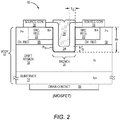
- Figure 2 shows the metal for the gate contact 26 completely, or at least substantially, fills any trench left over after the dielectric layer 24 has been deposited on the bottom and side walls of the trench 20.
- Figure 2 illustrates the bottom thickness T B of the dielectric layer 24 on the bottom of the trench 20 is approximately equal to the side thickness Ts of the dielectric layer 24 on the side walls of the trench 20.
- the side walls of the trench 20 form an angle ⁇ of less than 90° with the top surface, such that the trench is generally V-shaped. As such, the side walls of the trench 20 do not need to be orthogonal to the top surface of the body 12.
- the bottom thickness T B of the dielectric layer 24 on the bottom of the trench 20 is approximately 100%, or two times, greater than the side thickness Ts of the dielectric layer 24 on the side walls of the trench 20.
- the bottom thickness T B of the dielectric layer 24 on the bottom of the trench 20 may be between 80 and 100 nanometers (nm) while the side thickness Ts of the dielectric layer 24 on the side walls of the trench 20 may be between 40 and 50 nm.
- the bottom thickness T B may range between 20 and 200 nm or more, and the side thickness Ts may range between 10 and 50 nm, 5 and 100 nm, and 25 and 75 nm, depending on the desired performance parameters.
- an exemplary process is provided for forming the dielectric layer 24 such that the bottom thickness T B of the dielectric layer 24 on the bottom of the trench 20 is greater than the side thickness Ts of the dielectric layer 24 on the side walls of the trench 20.
- the process is performed on a field effect device precursor that includes the body 12 without the trench 20 being etched.
- the trench 20 is formed into the top surface of the body 12 wherein the top surface corresponds to the Si-face (0001) SiC (step 100).
- the trench 20 may be formed using standard etching processes, or perhaps a mechanical cutting process.
- the trench 20 will pass through the source regions 22 and the channel regions 18 into the drift region 16.
- the dielectric layer is deposited using a deposition process until the bottom thickness T B of the dielectric layer 24 on the bottom of the trench 20 and the side thickness Ts of the dielectric layer 24 on the side walls of the trench 20 reach desired levels (step 102).
- the bottom thickness T B of the dielectric layer 24 on the bottom of the trench 20 and the side thickness Ts of the dielectric layer 24 on the side walls of the trench 20 are more readily controlled.
- a deposition process allows the dielectric layer 24 to form such that the bottom thickness T B of the dielectric layer 24 on the bottom of the trench 20 is greater than the side thickness Ts of the dielectric layer 24 on the side walls of the trench 20.
- the bottom thickness T B of the dielectric layer 24 on the bottom of the trench 20 would undesirably end up much less than the side thickness Ts of the dielectric layer 24 on the side walls of the trench 20.
- the dielectric layer 24 may be silicon dioxide (SiO 2 ), aluminum oxide (AlO 2 ), magnesium oxide (MgO); or it may be formed from multiple layers of dielectric oxides or nitrides, from mixed alloys of similar dielectrics, or the like.
- a silicon dioxide (SiO 2 ) dielectric layer 24 is an effective match with SiC-based applications.
- the dielectric layer 24 may be annealed in an oxidant, such as oxygen (O 2 ), nitrous oxide (N 2 O), water, or the like (step 104).
- the annealing may take place at a relatively high temperature, such as between 1100 and 1300 Celsius (C) and last for 0.1 to 10 hours. This annealing step is optional in this exemplary process, but may be used to improve the insulating properties of the dielectric layer 24.
- the dielectric layer 24 is annealed in nitric oxide (NO) (step 106).
- This step of annealing in nitric oxide (NO) has been found to increase the density of the dielectric layer 24 and enhance the molecular interface between the dielectric layer 24 and the trench 20.
- Annealing with nitric oxide (NO) allows nitrogen (N) to build up at the interface between the dielectric layer 24 and the trench 20, and thus, provides nitrogen passivation PN (see Figures 1-3 , 5 , and 6 ) at the interface.
- the annealing may take place at a relatively high temperature, such as between 1100 and 1300 Celsius (C) and last for 0.5 to 5 hours.
- the gate contact 26 may be formed over the annealed dielectric layer 24 (step 108).
- the gate contact 26 may be formed in conjunction with forming the source contacts 28.
- the field effect device 10' is a SiC insulated gate bipolar transistor (IGBT), which has a body 32 that is configured similarly to the MOSFET described above.
- the gate assembly is formed in the same manner as that described above.
- the body 32 of the IGBT includes a substrate 34, a drift region 36 over the substrate 34, and a channel region 38 over the drift region 36.
- a trench 40 extends into the body 32 from a top surface of the body 32. As described above, the trench 40 may extend through the channel region 38 and into the drift region 36 to a depth d T . As such, the trench 40 divides the channel region 38. Emitter regions 42 are effectively formed in the channel regions 38 on either side of the trench 40.
- the substrate 34 may be a P-doped, single crystal, SiC substrate 34.
- the substrate 34 may be heavily doped with a P-type dopant at concentrations of between about 1x10 16 cm -3 and 1x10 19 cm -3 and have a thickness of between about 2 microns and 500 microns; however, the doping concentrations and thicknesses of the substrate 34 and the other layers may vary based on the desired parameters of the IGBT variant of the field effect device 10'.
- a SiC drift region 36 may be grown over the substrate 34 and doped in situ, wherein the drift region 36 is lightly doped as it is grown with an N-type doping material.
- one or more buffer layers may be formed on the substrate 34 prior to forming the drift region 36.
- the buffer layer(s) may be used as a nucleation layer and be relatively heavily doped with an N-type doping material.
- the drift region 36 may be relatively uniformly doped throughout or may employ graded doping throughout all or a portion thereof.
- the doping concentration may be between about 1x10 14 cm -3 and 1x10 16 cm -3 in one embodiment. With graded doping, the doping concentration is highest at the bottom of the drift region 36 near the substrate 34 and lowest at the top of the drift region 36. The doping concentration generally decreases in a stepwise or continuous fashion from a point at or near the bottom to a point at or near the top of the drift region 36.
- a SiC channel region 38 may be grown over the drift region 36 and doped in situ, wherein the channel region 38 is heavily doped as it is grown with a P-type doping material at concentrations between about 1x10 17 cm -3 and 5x10 18 cm -3 .
- the emitter regions 42 Prior to a trench 40 being formed, the emitter regions 42 are effectively created as a single emitter well in the channel region 38 and heavily doped with an N-type doping material.
- the trench 40 is etched from the top surface of the body 32 through the central portion of the emitter well and the channel region 38 and into the drift region 36. As a result, a channel region 38 and an emitter region 42 are provided on each side of the trench 40. Both side walls of the trench 40 are formed from portions of the emitter region 42, the channel regions 38, and the drift region 36.
- One or more collector contacts 50 are provided on the bottom surface of the substrate 34.
- the bottom of the trench 40 resides in the drift region 36 and extends between the lower ends of the side walls of the trench 40.
- the side walls of the trench 40 are substantially orthogonal to the top surface of the body 32, and the bottom of the trench 40 is substantially parallel to the top surface of the body 32.
- the corners between the bottom and the side walls of the trench 40 are rounded to reduce electric field concentrations, which would be higher with sharper corners.
- the gate assembly for the IGBT is formed in the trench 40 and includes a uniquely formed dielectric layer 44 and a gate contact 46.
- the dielectric layer 44 is formed substantially continuously along the side walls and bottom of the trench 40.
- the gate contact 46 is formed on the dielectric layer 44.
- the bottom thickness T B of the dielectric layer 44 on the bottom of the trench 40 is greater than the side thickness Ts of the dielectric layer 24 on the side walls of the trench 40.
- Figure 6 shows the metal for the gate contact 46 completely, or at least substantially, fills any trench left over after the dielectric layer 44 has been deposited on the bottom and side walls of the trench 40.
- Figure 6 illustrates wherein the bottom thickness T B of the dielectric layer 44 on the bottom of the trench 40 is approximately equal to the side thickness Ts of the dielectric layer 44 on the side walls of the trench 40.
- the trench 40 may be created such that the side walls of the trench 40 form an angle ⁇ of less than 90° with the top surface, such that the trench is generally V-shaped.
Landscapes
- Electrodes Of Semiconductors (AREA)
- Insulated Gate Type Field-Effect Transistor (AREA)
Abstract
Description
- The present disclosure relates to enhanced gate dielectrics for field effect devices.
- Semiconductor devices, especially those designed to block high voltages and conduct large currents in high power applications, are subjected to powerful electrical forces and electromagnetic fields at the molecular level. Further, these devices may be subjected to high temperatures during fabrication and operation. These forces, fields, and temperatures can damage the molecular structure of the various layers and regions within the device, as well as the interface between these various layers or regions. Such damage leads to device failures as well as degraded performance over time. For field effect devices employing a metallized gate that is separated from the body of the device by a dielectric layer, the dielectric layer and the interface between the dielectric layer and the body are particularly vulnerable. As such, there is a need for a gate dielectric for a field effect device that is less vulnerable to the forces and fields that are generated in high voltage and current applications as well as the potentially damaging temperatures associated with fabrication and operation.
US 2012/0248462 discloses an IGBT including a groove in a silicon carbide semiconductor layer, a body region of a first conductivity type provided in the silicon carbide semiconductor layer, and an insulating film covering at least a sidewall surface of the groove, the sidewall surface of the groove being a surface having an off angle of 50° or more and 65° or less with respect to a {0001} plane. The sidewall surface of the groove includes a surface of the body region, the insulating film being in contact with at least the surface of the body region at the sidewall surface of the groove, and a first conductivity type impurity concentration in the body region being 5x1016 cm-3 or more.
US 2011/017998 A1 discloses a trench gate vertical power device. A gate insulating film is integrally formed in the trench and has a bottom portion and a side portion. The thickness of the bottom portion is greater than the thickness of the side portion. The gate insulating film is formed through a oxidation of SiC semiconductor material.
Vertical power devices are also known from the documentsUS 2013/146969A1 ,US 2007/057262A1 ,EP1,981,076A1 ,US 2012/286291A1 andJP 2008-11406A - The present disclosure relates to a silicon carbide (SiC) field effect device that has a gate assembly formed in a trench. The gate assembly includes a gate dielectric that is a dielectric layer, which is deposited along the inside surface of the trench, and a gate dielectric formed over the gate dielectric. The trench extends into the body of the device from a top surface, has a bottom, and has side walls that extend from the top surface of the body to the bottom of the trench. The thickness of the dielectric layer on the bottom surface may exceed that of the side walls by between 25% and 100%. The side walls may be substantially orthogonal to the top surface or may form an angle of less than 90° with the top surface, such that the trench is generally V-shaped.
- In one embodiment, a nitrogen passivation is provided at the interface between the dielectric layer and the trench due to the dielectric layer being annealed with nitric oxide (NO). The nitrogen passivation provides an excellent interface between the dielectric layer and the trench. The dielectric layer may be silicon dioxide (SiO2), aluminum oxide (AlO2), magnesium oxide (MgO), or the like. Alternatively, the dielectric layer may be formed from multiple layers of dielectric oxides, nitrides, or both as well as mixed alloys of similar dielectrics.
- An exemplary process for forming the field effect device includes providing a field effect device precursor that includes a body and forming the trench into the top surface of the body using an etching or mechanical cutting process. Next, the dielectric layer for the gate dielectric is deposited, as opposed to thermally grown, using an evaporative process. The dielectric layer may be annealed in an oxidant, such as oxygen (O2), nitrous oxide (N2O), water, or the like. This annealing step is optional, but may be used to improve the insulating properties of the gate dielectric. The dielectric layer is then annealed in nitric oxide (NO) to increase the density of the dielectric layer, enhance the interface between the dielectric layer and the trench, or both. Annealing with nitric oxide (NO) allows nitrogen (N) to build up at the interface between the dielectric layer and the trench, and thus, provide the nitrogen passivation at the interface.
- Those skilled in the art will appreciate the scope of the present disclosure and realize additional aspects thereof after reading the following detailed description of the preferred embodiments in association with the accompanying drawing figures.
- The accompanying drawing figures incorporated in and forming a part of this specification illustrate several aspects of the disclosure, and together with the description serve to explain the principles of the disclosure.
-
Figure 1 illustrates a MOSFET that has a gate structure formed according to a first embodiment of the present disclosure. -
Figure 2 illustrates a MOSFET where the metal for a gate contact fills any trench left over after the dielectric layer has been deposited on the bottom and side walls of a trench. -
Figure 3 illustrates a MOSFET that has a gate structure formed according to a second embodiment of the present disclosure. -
Figure 4 illustrates one process for forming the gate structure of the embodiments provided inFigures 1 and3 . -
Figure 5 illustrates an IGBT that has a gate structure formed according to a third embodiment of the present disclosure. -
Figure 6 illustrates an IGBT where the metal for a gate structure fills any trench left over after the dielectric layer has been deposited on the bottom and side walls of a trench. -
Figure 7 illustrates an IGBT that has a gate structure formed according to a fourth embodiment of the present disclosure. - It will be understood that, although the terms first, second, etc. may be used herein to describe various elements, these elements should not be limited by these terms. These terms are only used to distinguish one element from another. For example, a first element could be termed a second element, and, similarly, a second element could be termed a first element, without departing from the scope of the present disclosure. As used herein, the term "and/or" includes any and all combinations of one or more of the associated listed items.
- It will be understood that when an element such as a layer, region, or substrate is referred to as being "on" or extending "onto" another element, it can be directly on or extend directly onto the other element or intervening elements may also be present. In contrast, when an element is referred to as being "directly on" or extending "directly onto" another element, there are no intervening elements present. Likewise, it will be understood that when an element such as a layer, region, or substrate is referred to as being "over" or extending "over" another element, it can be directly over or extend directly over the other element or intervening elements may also be present. In contrast, when an element is referred to as being "directly over" or extending "directly over" another element, there are no intervening elements present. It will also be understood that when an element is referred to as being "connected" or "coupled" to another element, it can be directly connected or coupled to the other element or intervening elements may be present. In contrast, when an element is referred to as being "directly connected" or "directly coupled" to another element, there are no intervening elements present.
- Relative terms such as "below" or "above" or "upper" or "lower" or "horizontal" or "vertical" may be used herein to describe a relationship of one element, layer, or region to another element, layer, or region as illustrated in the Figures. It will be understood that these terms and those discussed above are intended to encompass different orientations of the device in addition to the orientation depicted in the Figures.
- The terminology used herein is for the purpose of describing particular embodiments only and is not intended to be limiting of the disclosure. As used herein, the singular forms "a," "an," and "the" are intended to include the plural forms as well, unless the context clearly indicates otherwise. It will be further understood that the terms "comprises," "comprising," "includes," and/or "including" when used herein specify the presence of stated features, integers, steps, operations, elements, and/or components, but do not preclude the presence or addition of one or more other features, integers, steps, operations, elements, components, and/or groups thereof.
- Unless otherwise defined, all terms (including technical and scientific terms) used herein have the same meaning as commonly understood by one of ordinary skill in the art to which this disclosure belongs. It will be further understood that terms used herein should be interpreted as having a meaning that is consistent with their meaning in the context of this specification and the relevant art and will not be interpreted in an idealized or overly formal sense unless expressly so defined herein.
- With reference to
Figure 1 , a first embodiment of afield effect device 10 is illustrated. The field effect device is a silicon carbide (SiC) metal oxide field effect transistor (MOSFET) that has abody 12, which includes asubstrate 14, adrift region 16 over thesubstrate 14, and achannel region 18 over thedrift region 16. Atrench 20 extends into thebody 12 from a top surface of thebody 12. As illustrated, thetrench 20 may extend through thechannel region 18 and into thedrift region 16 to a depth dT. As such, thetrench 20 divides thechannel region 18.Source regions 22 are effectively formed in thechannel regions 18 on either side of thetrench 20. - The
substrate 14 may be an N-doped, single crystal,SiC substrate 14. Thesubstrate 14 may have various crystalline polytypes, such as 2H, 4H, 6H, 3C and the like. In other embodiments, thesubstrate 14 may also be formed from other material systems, such as gallium nitride (GaN), gallium arsenide (GaAs), silicon (Si), germanium (Ge), SiGe, and the like. The substrate may be heavily doped with an N-type dopant at concentrations of between about 1x1017 cm-3 and 1x1019 cm-3 and have a thickness of between about 100 microns and 600 microns; however, the doping concentrations and thicknesses of thesubstrate 14 and the other layers may vary based on the desired parameters of thefield effect device 10. - A
SiC drift region 16 may be grown over thesubstrate 14 and doped in situ, wherein thedrift region 16 is lightly doped as it is grown with an N-type doping material. Notably, one or more buffer layers (not shown) may be formed on thesubstrate 14 prior to forming thedrift region 16. The buffer layer(s) may be used as a nucleation layer and be relatively heavily doped with an N-type doping material. - The
drift region 16 may be relatively uniformly doped throughout or may employ graded doping throughout all or a portion thereof. For a uniformly dopeddrift region 16, the doping concentration may be between about 1x1014 cm-3 and 1x1016 cm-3 in one embodiment. With graded doping, the doping concentration is highest at the bottom of thedrift region 16 near thesubstrate 14 and lowest at the top of thedrift region 16. The doping concentration generally decreases in a stepwise or continuous fashion from a point at or near the bottom to a point at or near the top of thedrift region 16. In one embodiment employing graded doping, the lower portion of the drift region16 may be doped at a concentration of about 1x1014 cm-3 and the upper portion of thedrift region 16 may be doped at a concentration of about 1x1016 cm-3. Thedrift region 16 may be between four and ten microns thick in select embodiments depending on the desired parameters of thefield effect device 10. - A
SiC channel region 18 may be grown over thedrift region 16 and doped in situ, wherein thechannel region 18 is heavily doped as it is grown with a P-type doping material at concentrations between about 1x1017 cm-3 and 5x1018 cm-3. Thechannel region 18 at its thickest point may be between about 1 microns and 5 microns. Prior to thetrench 20 being formed, thesource regions 22 are effectively created as a single source well in thechannel region 18 and heavily doped with an N-type doping material. - The
trench 20 is etched from the top surface of thebody 12 through the central portion of the source well and thechannel region 18 and into thedrift region 16. As a result, achannel region 18 and asource region 22 are provided on each side of thetrench 20. Both side walls of thetrench 20 are formed from portions of thesource region 22, thechannel regions 18, and thedrift region 16. The bottom of thetrench 20 resides in thedrift region 16 and extends between the lower ends of the side walls of thetrench 20. In the embodiment ofFigure 1 , the side walls of thetrench 20 are substantially orthogonal to the top surface of thebody 12, and the bottom of thetrench 20 is substantially parallel to the top surface of thebody 12. In one embodiment, the corners between the bottom and the side walls of thetrench 20 are rounded to reduce electric field concentrations, which would be higher with sharper corners. - The gate assembly for the
field effect device 10 is formed in thetrench 20 and includes a uniquely formeddielectric layer 24 and agate contact 26. Thedielectric layer 24 is formed substantially continuously along the side walls and bottom of thetrench 20. Thegate contact 26 is formed on thedielectric layer 24. Thedielectric layer 24 may be an oxide, such as silicon dioxide (SiO2), aluminum oxide (AlO2), magnesium oxide (MgO). Alternatively, thedielectric layer 24 may be formed from multiple layers of dielectric oxides, nitrides, or both as well as mixed alloys of similar dielectrics. For the following example, thedielectric layer 24 is an oxide. Thegate contact 26 is generally relatively thick and formed from a highly doped semiconductor such as Si or Ge, or a metal, such as aluminum (Al), gold (Au), Silver (Ag), and the like. - Unlike other SiC-based field effect devices with a gate assembly formed in a trench, the bottom thickness TB of the
dielectric layer 24 on the bottom of thetrench 20 is greater than the side thickness Ts of thedielectric layer 24 on the side walls of thetrench 20. For example, the thickness of thedielectric layer 24 on the bottom surface may exceed that of the side walls by 25% or more, 50% or more, or even 100%. As illustrated, the bottom of thetrench 20 is approximately 100%, or two times, greater than the side thickness Ts of thedielectric layer 24 on the side walls of thetrench 20. - In conventional SiC field effect devices, the dielectric layer is grown using a thermal growth process. With a thermal growth process where the trench is etched into the Si-face (0001) SiC, the growth rate of the oxide on the bottom (Si-face (0001)) of the trench is around three times slower than that on the side walls, which may reside in the a-face {11-20} and m-face {10-10} family of planes. As a result, the thickness of the dielectric layer on the side walls is much thicker than the dielectric layer on the bottom of the trench. The thicker dielectric layer on the side walls leads to higher electric fields along the portion of the dielectric layer that is formed on the bottom of the trench than along the portions of the dielectric layer that are formed on the side walls of the trench. The higher electric fields along the portion of the dielectric layer along the bottom of the trench leads to device failure, and thus, reduces the long-term reliability of the field effect device.
- To improve reliability, the present disclosure provides for the bottom thickness TB of the
dielectric layer 24 on the bottom of thetrench 20 to be greater than the side thickness Ts of thedielectric layer 24 on the side walls of thetrench 20. As illustrated in the embodiment ofFigure 1 , the bottom thickness TB of thedielectric layer 24 on the bottom of thetrench 20 is substantially greater than the side thickness Ts of thedielectric layer 24 on the side walls of thetrench 20. A unique process for forming thedielectric layer 24 in this manner is provided further below. - With continued reference to
Figure 1 , the MOSFET embodiment of thefield effect device 10 includessource contacts 28 on therespective source regions 22 and one ormore drain contacts 30 on the bottom surface of thesubstrate 14. Like thegate contact 26, the source anddrain contacts - In the embodiment of
Figure 1 , the width of thetrench 20 and the thicknesses of thedielectric layer 24 and the metal for thegate contact 26 on the side walls is such that thegate contact 26 is U-shaped. As such, an open trench is formed by thegate contact 26. Other materials may fill the open trench during subsequent processing steps. -
Figure 2 shows the metal for thegate contact 26 completely, or at least substantially, fills any trench left over after thedielectric layer 24 has been deposited on the bottom and side walls of thetrench 20.Figure 2 illustrates the bottom thickness TB of thedielectric layer 24 on the bottom of thetrench 20 is approximately equal to the side thickness Ts of thedielectric layer 24 on the side walls of thetrench 20. - With reference to
Figure 3 , an embodiment is illustrated wherein the side walls of thetrench 20 form an angle α of less than 90° with the top surface, such that the trench is generally V-shaped. As such, the side walls of thetrench 20 do not need to be orthogonal to the top surface of thebody 12. In the illustrated embodiment, the bottom thickness TB of thedielectric layer 24 on the bottom of thetrench 20 is approximately 100%, or two times, greater than the side thickness Ts of thedielectric layer 24 on the side walls of thetrench 20. For example, the bottom thickness TB of thedielectric layer 24 on the bottom of thetrench 20 may be between 80 and 100 nanometers (nm) while the side thickness Ts of thedielectric layer 24 on the side walls of thetrench 20 may be between 40 and 50 nm. - While keeping within the confines of the bottom thickness TB being substantially greater than the side thickness Ts, the bottom thickness TB may range between 20 and 200 nm or more, and the side thickness Ts may range between 10 and 50 nm, 5 and 100 nm, and 25 and 75 nm, depending on the desired performance parameters.
- With reference to the flow diagram of
Figure 4 , an exemplary process is provided for forming thedielectric layer 24 such that the bottom thickness TB of thedielectric layer 24 on the bottom of thetrench 20 is greater than the side thickness Ts of thedielectric layer 24 on the side walls of thetrench 20. The process is performed on a field effect device precursor that includes thebody 12 without thetrench 20 being etched. Initially, thetrench 20 is formed into the top surface of thebody 12 wherein the top surface corresponds to the Si-face (0001) SiC (step 100). Thetrench 20 may be formed using standard etching processes, or perhaps a mechanical cutting process. Thetrench 20 will pass through thesource regions 22 and thechannel regions 18 into thedrift region 16. - Once the
trench 20 is formed, the dielectric layer is deposited using a deposition process until the bottom thickness TB of thedielectric layer 24 on the bottom of thetrench 20 and the side thickness Ts of thedielectric layer 24 on the side walls of thetrench 20 reach desired levels (step 102). By using an evaporative process, as opposed to a thermal growth process, the bottom thickness TB of thedielectric layer 24 on the bottom of thetrench 20 and the side thickness Ts of thedielectric layer 24 on the side walls of thetrench 20 are more readily controlled. Unlike a thermal growth process, a deposition process allows thedielectric layer 24 to form such that the bottom thickness TB of thedielectric layer 24 on the bottom of thetrench 20 is greater than the side thickness Ts of thedielectric layer 24 on the side walls of thetrench 20. If a thermal growth process were used to form thedielectric layer 24 in thetrench 20 of a SiC-basedbody 12, the bottom thickness TB of thedielectric layer 24 on the bottom of thetrench 20 would undesirably end up much less than the side thickness Ts of thedielectric layer 24 on the side walls of thetrench 20. Depending on the embodiment, thedielectric layer 24 may be silicon dioxide (SiO2), aluminum oxide (AlO2), magnesium oxide (MgO); or it may be formed from multiple layers of dielectric oxides or nitrides, from mixed alloys of similar dielectrics, or the like. A silicon dioxide (SiO2)dielectric layer 24 is an effective match with SiC-based applications. - After the
dielectric layer 24 is deposited, the dielectric layer may be annealed in an oxidant, such as oxygen (O2), nitrous oxide (N2O), water, or the like (step 104). The annealing may take place at a relatively high temperature, such as between 1100 and 1300 Celsius (C) and last for 0.1 to 10 hours. This annealing step is optional in this exemplary process, but may be used to improve the insulating properties of thedielectric layer 24. - Next, the
dielectric layer 24 is annealed in nitric oxide (NO) (step 106). This step of annealing in nitric oxide (NO) has been found to increase the density of thedielectric layer 24 and enhance the molecular interface between thedielectric layer 24 and thetrench 20. Annealing with nitric oxide (NO) allows nitrogen (N) to build up at the interface between thedielectric layer 24 and thetrench 20, and thus, provides nitrogen passivation PN (seeFigures 1-3 ,5 , and6 ) at the interface. The annealing may take place at a relatively high temperature, such as between 1100 and 1300 Celsius (C) and last for 0.5 to 5 hours. - Finally, the
gate contact 26 may be formed over the annealed dielectric layer 24 (step 108). Thegate contact 26 may be formed in conjunction with forming thesource contacts 28. - With reference to
Figure 5 , a third embodiment of a field effect device 10' is illustrated. The field effect device 10' is a SiC insulated gate bipolar transistor (IGBT), which has abody 32 that is configured similarly to the MOSFET described above. The gate assembly is formed in the same manner as that described above. Thebody 32 of the IGBT includes asubstrate 34, adrift region 36 over thesubstrate 34, and achannel region 38 over thedrift region 36. Atrench 40 extends into thebody 32 from a top surface of thebody 32. As described above, thetrench 40 may extend through thechannel region 38 and into thedrift region 36 to a depth dT. As such, thetrench 40 divides thechannel region 38.Emitter regions 42 are effectively formed in thechannel regions 38 on either side of thetrench 40. - In contrast with the MOSFET, the
substrate 34 may be a P-doped, single crystal,SiC substrate 34. Thesubstrate 34 may be heavily doped with a P-type dopant at concentrations of between about 1x1016 cm-3 and 1x1019 cm-3 and have a thickness of between about 2 microns and 500 microns; however, the doping concentrations and thicknesses of thesubstrate 34 and the other layers may vary based on the desired parameters of the IGBT variant of the field effect device 10'. - A
SiC drift region 36 may be grown over thesubstrate 34 and doped in situ, wherein thedrift region 36 is lightly doped as it is grown with an N-type doping material. Notably, one or more buffer layers (not shown) may be formed on thesubstrate 34 prior to forming thedrift region 36. The buffer layer(s) may be used as a nucleation layer and be relatively heavily doped with an N-type doping material. - The
drift region 36 may be relatively uniformly doped throughout or may employ graded doping throughout all or a portion thereof. For a uniformly dopeddrift region 36, the doping concentration may be between about 1x1014 cm-3 and 1x1016 cm-3 in one embodiment. With graded doping, the doping concentration is highest at the bottom of thedrift region 36 near thesubstrate 34 and lowest at the top of thedrift region 36. The doping concentration generally decreases in a stepwise or continuous fashion from a point at or near the bottom to a point at or near the top of thedrift region 36. - A
SiC channel region 38 may be grown over thedrift region 36 and doped in situ, wherein thechannel region 38 is heavily doped as it is grown with a P-type doping material at concentrations between about 1x1017 cm-3 and 5x1018 cm-3. Prior to atrench 40 being formed, theemitter regions 42 are effectively created as a single emitter well in thechannel region 38 and heavily doped with an N-type doping material. - The
trench 40 is etched from the top surface of thebody 32 through the central portion of the emitter well and thechannel region 38 and into thedrift region 36. As a result, achannel region 38 and anemitter region 42 are provided on each side of thetrench 40. Both side walls of thetrench 40 are formed from portions of theemitter region 42, thechannel regions 38, and thedrift region 36. One ormore collector contacts 50 are provided on the bottom surface of thesubstrate 34. - The bottom of the
trench 40 resides in thedrift region 36 and extends between the lower ends of the side walls of thetrench 40. In the embodiment ofFigure 5 , the side walls of thetrench 40 are substantially orthogonal to the top surface of thebody 32, and the bottom of thetrench 40 is substantially parallel to the top surface of thebody 32. As noted above, the corners between the bottom and the side walls of thetrench 40 are rounded to reduce electric field concentrations, which would be higher with sharper corners. - As with the MOSFET embodiment, the gate assembly for the IGBT is formed in the
trench 40 and includes a uniquely formeddielectric layer 44 and agate contact 46. Thedielectric layer 44 is formed substantially continuously along the side walls and bottom of thetrench 40. Thegate contact 46 is formed on thedielectric layer 44. As noted above, the bottom thickness TB of thedielectric layer 44 on the bottom of thetrench 40 is greater than the side thickness Ts of thedielectric layer 24 on the side walls of thetrench 40. -
Figure 6 shows the metal for thegate contact 46 completely, or at least substantially, fills any trench left over after thedielectric layer 44 has been deposited on the bottom and side walls of thetrench 40.Figure 6 illustrates wherein the bottom thickness TB of thedielectric layer 44 on the bottom of thetrench 40 is approximately equal to the side thickness Ts of thedielectric layer 44 on the side walls of thetrench 40. - As another variant that is illustrated in
Figure 7 , thetrench 40 may be created such that the side walls of thetrench 40 form an angle α of less than 90° with the top surface, such that the trench is generally V-shaped.
Claims (13)
- A field effect device comprising:» a body (12, 32) having a top surface and a trench (20, 40) extending into the body from the top surface wherein the trench has a bottom and a plurality of side walls;• a deposited dielectric layer (24, 44) formed substantially along the plurality of side walls to a first thickness (Ts) and the bottom of the trench to a second thickness (TB), the deposited dielectric layer being formed via a single evaporative process such that the second thickness of the deposited dielectric layer on the bottom of the trench is substantially greater than the first thickness of the deposited dielectric layer on the plurality of side walls of the trench, where the second thickness has a thickness in a range between 25% greater than the first thickness and 100% greater than the first thickness; and• a gate contact (26, 46) formed over the deposited dielectric layer wherein the deposited dielectric layer and the gate contact form a gate assembly for the field effect device and the body comprises silicon carbide.
- The field effect device of claim 1 wherein the deposited dielectric layer is a nitric oxide annealed deposited dielectric layer.
- The field effect device of claim 1 wherein a nitrogen passivation is provided at an interface between the deposited dielectric layer and the inside surface of the trench.
- The field effect device of claim 1 wherein the deposited dielectric layer is silicon dioxide.
- The field effect device of claim 1 wherein the deposited dielectric layer is silicon dioxide, the deposited dielectric layer is a nitric oxide annealed deposited dielectric layer, and a nitrogen passivation is provided at an interface between the deposited dielectric layer and the inside surface of the trench.
- The field effect device of claim 1 wherein the body comprises a substrate (14, 34), a drift region (16, 36) over the substrate, and channel regions (18, 38) on either side of the trench.
- The field effect device of claim 6 wherein the trench extends into the drift region.
- The field effect device of claim 7 wherein at least one of source (28) or emitter (48) contacts are provided over the top surface on either side of the trench and at least one of a drain (30) or collector (50) contact is provided over a bottom surface of the substrate.
- The field effect device of claim 1 wherein the field effect device is a metal oxide semiconductor field effect device.
- The field effect device of claim 1 wherein the field effect device is an insulated gate bipolar transistor.
- The field effect device of claim 1 wherein the plurality of side walls are substantially perpendicular to the top surface.
- The field effect device of claim 1 wherein the bottom is substantially parallel with the top surface.
- The field effect device of claim 1 wherein the trench is generally V-shaped.
Applications Claiming Priority (3)
| Application Number | Priority Date | Filing Date | Title |
|---|---|---|---|
| US13/944,473 US9570570B2 (en) | 2013-07-17 | 2013-07-17 | Enhanced gate dielectric for a field effect device with a trenched gate |
| EP14830427.2A EP3022772B1 (en) | 2013-07-17 | 2014-07-14 | Enhanced gate dielectric for a field effect device with a trenched gate |
| PCT/US2014/046505 WO2015050615A2 (en) | 2013-07-17 | 2014-07-14 | Enhanced gate dielectric for a field effect device with a trenched gate |
Related Parent Applications (2)
| Application Number | Title | Priority Date | Filing Date |
|---|---|---|---|
| EP14830427.2A Division EP3022772B1 (en) | 2013-07-17 | 2014-07-14 | Enhanced gate dielectric for a field effect device with a trenched gate |
| EP14830427.2A Division-Into EP3022772B1 (en) | 2013-07-17 | 2014-07-14 | Enhanced gate dielectric for a field effect device with a trenched gate |
Publications (1)
| Publication Number | Publication Date |
|---|---|
| EP3826073A1 true EP3826073A1 (en) | 2021-05-26 |
Family
ID=52342857
Family Applications (2)
| Application Number | Title | Priority Date | Filing Date |
|---|---|---|---|
| EP14830427.2A Active EP3022772B1 (en) | 2013-07-17 | 2014-07-14 | Enhanced gate dielectric for a field effect device with a trenched gate |
| EP20213192.6A Pending EP3826073A1 (en) | 2013-07-17 | 2014-07-14 | Enhanced gate dielectric for a field effect device with a trenched gate |
Family Applications Before (1)
| Application Number | Title | Priority Date | Filing Date |
|---|---|---|---|
| EP14830427.2A Active EP3022772B1 (en) | 2013-07-17 | 2014-07-14 | Enhanced gate dielectric for a field effect device with a trenched gate |
Country Status (4)
| Country | Link |
|---|---|
| US (1) | US9570570B2 (en) |
| EP (2) | EP3022772B1 (en) |
| JP (1) | JP2016528729A (en) |
| WO (1) | WO2015050615A2 (en) |
Families Citing this family (9)
| Publication number | Priority date | Publication date | Assignee | Title |
|---|---|---|---|---|
| JP2016164906A (en) * | 2015-03-06 | 2016-09-08 | 豊田合成株式会社 | Semiconductor device and manufacturing method of the same, and power converter |
| US9991379B1 (en) | 2016-11-17 | 2018-06-05 | Sanken Electric Co., Ltd. | Semiconductor device with a gate insulating film formed on an inner wall of a trench, and method of manufacturing the same |
| DE102016015475B3 (en) * | 2016-12-28 | 2018-01-11 | 3-5 Power Electronics GmbH | IGBT semiconductor structure |
| US12641822B2 (en) | 2020-06-19 | 2026-05-26 | Wolfspeed, Inc. | Power devices with a hybrid gate structure |
| US11355630B2 (en) * | 2020-09-11 | 2022-06-07 | Wolfspeed, Inc. | Trench bottom shielding methods and approaches for trenched semiconductor device structures |
| US11640990B2 (en) | 2020-10-27 | 2023-05-02 | Wolfspeed, Inc. | Power semiconductor devices including a trenched gate and methods of forming such devices |
| JP7697286B2 (en) * | 2021-06-21 | 2025-06-24 | 富士電機株式会社 | Silicon carbide semiconductor device and method for manufacturing silicon carbide semiconductor device |
| JP7697313B2 (en) * | 2021-08-17 | 2025-06-24 | 富士電機株式会社 | Silicon carbide semiconductor device and method for manufacturing silicon carbide semiconductor device |
| US20260231468A1 (en) | 2025-01-31 | 2026-08-06 | Wolfspeed, Inc. | Power semiconductor devices having high dielectric constant gate dielectric layers and thinned shielding patterns |
Citations (10)
| Publication number | Priority date | Publication date | Assignee | Title |
|---|---|---|---|---|
| US20040211980A1 (en) * | 2003-04-24 | 2004-10-28 | Sei-Hyung Ryu | Silicon carbide power devices with self-aligned source and well regions and methods of fabricating same |
| US20070057262A1 (en) | 2005-09-12 | 2007-03-15 | Fuji Electric Holding Co., Ltd. | Semicoductor device and manufacturing method thereof |
| JP2008011406A (en) | 2006-06-30 | 2008-01-17 | Toshiba Corp | Receiver and transmitter |
| EP1981076A1 (en) | 2006-01-30 | 2008-10-15 | Sumitomo Electric Industries, Ltd. | Method for manufacturing silicon carbide semiconductor device |
| JP2008311406A (en) * | 2007-06-14 | 2008-12-25 | Toyota Motor Corp | Manufacturing method of trench gate type SiC semiconductor device |
| US20110017998A1 (en) | 2009-07-21 | 2011-01-27 | Rohm Co., Ltd. | Semiconductor device |
| US20120248462A1 (en) | 2011-03-30 | 2012-10-04 | Sumitomo Electric Industries, Ltd. | Igbt |
| US20120286291A1 (en) | 2010-03-12 | 2012-11-15 | Sumitomo Electric Industries, Ltd. | Silicon carbide semiconductor device and method for manufacturing the same |
| US20130119407A1 (en) * | 2011-11-16 | 2013-05-16 | Sumitomo Electric Industries, Ltd. | Method for manufacturing semiconductor device, and semiconductor device |
| US20130146969A1 (en) | 2011-12-13 | 2013-06-13 | Hirokazu Fujiwara | Switching element and manufacturing method thereof |
Family Cites Families (12)
| Publication number | Priority date | Publication date | Assignee | Title |
|---|---|---|---|---|
| JP3123061B2 (en) * | 1990-06-13 | 2001-01-09 | ソニー株式会社 | Buried flattening method by bias ECR-CVD method |
| US5382541A (en) * | 1992-08-26 | 1995-01-17 | Harris Corporation | Method for forming recessed oxide isolation containing deep and shallow trenches |
| JP3419163B2 (en) * | 1995-09-06 | 2003-06-23 | 株式会社デンソー | Method for manufacturing silicon carbide semiconductor device |
| US6573534B1 (en) * | 1995-09-06 | 2003-06-03 | Denso Corporation | Silicon carbide semiconductor device |
| JP5116910B2 (en) * | 1999-02-23 | 2013-01-09 | パナソニック株式会社 | Method for manufacturing insulated gate type semiconductor device |
| US6291298B1 (en) * | 1999-05-25 | 2001-09-18 | Advanced Analogic Technologies, Inc. | Process of manufacturing Trench gate semiconductor device having gate oxide layer with multiple thicknesses |
| US6696726B1 (en) * | 2000-08-16 | 2004-02-24 | Fairchild Semiconductor Corporation | Vertical MOSFET with ultra-low resistance and low gate charge |
| GB0312512D0 (en) * | 2003-05-31 | 2003-07-09 | Koninkl Philips Electronics Nv | Termination structures for semiconductor devices and the manufacture thereof |
| US20090142899A1 (en) * | 2007-12-04 | 2009-06-04 | Jensen Jacob M | Interfacial layer for hafnium-based high-k/metal gate transistors |
| JP4911263B2 (en) * | 2009-03-11 | 2012-04-04 | 三菱電機株式会社 | Method for manufacturing silicon carbide semiconductor device |
| JP6037499B2 (en) * | 2011-06-08 | 2016-12-07 | ローム株式会社 | Semiconductor device and manufacturing method thereof |
| JP5751113B2 (en) * | 2011-09-28 | 2015-07-22 | 住友電気工業株式会社 | Method for manufacturing silicon carbide semiconductor device |
-
2013
- 2013-07-17 US US13/944,473 patent/US9570570B2/en active Active
-
2014
- 2014-07-14 WO PCT/US2014/046505 patent/WO2015050615A2/en not_active Ceased
- 2014-07-14 JP JP2016527010A patent/JP2016528729A/en active Pending
- 2014-07-14 EP EP14830427.2A patent/EP3022772B1/en active Active
- 2014-07-14 EP EP20213192.6A patent/EP3826073A1/en active Pending
Patent Citations (10)
| Publication number | Priority date | Publication date | Assignee | Title |
|---|---|---|---|---|
| US20040211980A1 (en) * | 2003-04-24 | 2004-10-28 | Sei-Hyung Ryu | Silicon carbide power devices with self-aligned source and well regions and methods of fabricating same |
| US20070057262A1 (en) | 2005-09-12 | 2007-03-15 | Fuji Electric Holding Co., Ltd. | Semicoductor device and manufacturing method thereof |
| EP1981076A1 (en) | 2006-01-30 | 2008-10-15 | Sumitomo Electric Industries, Ltd. | Method for manufacturing silicon carbide semiconductor device |
| JP2008011406A (en) | 2006-06-30 | 2008-01-17 | Toshiba Corp | Receiver and transmitter |
| JP2008311406A (en) * | 2007-06-14 | 2008-12-25 | Toyota Motor Corp | Manufacturing method of trench gate type SiC semiconductor device |
| US20110017998A1 (en) | 2009-07-21 | 2011-01-27 | Rohm Co., Ltd. | Semiconductor device |
| US20120286291A1 (en) | 2010-03-12 | 2012-11-15 | Sumitomo Electric Industries, Ltd. | Silicon carbide semiconductor device and method for manufacturing the same |
| US20120248462A1 (en) | 2011-03-30 | 2012-10-04 | Sumitomo Electric Industries, Ltd. | Igbt |
| US20130119407A1 (en) * | 2011-11-16 | 2013-05-16 | Sumitomo Electric Industries, Ltd. | Method for manufacturing semiconductor device, and semiconductor device |
| US20130146969A1 (en) | 2011-12-13 | 2013-06-13 | Hirokazu Fujiwara | Switching element and manufacturing method thereof |
Also Published As
| Publication number | Publication date |
|---|---|
| US20150021623A1 (en) | 2015-01-22 |
| WO2015050615A3 (en) | 2015-05-28 |
| JP2016528729A (en) | 2016-09-15 |
| US9570570B2 (en) | 2017-02-14 |
| WO2015050615A2 (en) | 2015-04-09 |
| EP3022772B1 (en) | 2021-02-17 |
| EP3022772A2 (en) | 2016-05-25 |
Similar Documents
| Publication | Publication Date | Title |
|---|---|---|
| EP3022772B1 (en) | Enhanced gate dielectric for a field effect device with a trenched gate | |
| US10256294B2 (en) | Vertical gallium nitride power field-effect transistor with a field plate structure | |
| US8841741B2 (en) | High breakdown voltage semiconductor rectifier | |
| US9318619B2 (en) | Vertical gallium nitride JFET with gate and source electrodes on regrown gate | |
| JP5671779B2 (en) | Epitaxial wafer manufacturing method and semiconductor device manufacturing method | |
| US9502544B2 (en) | Method and system for planar regrowth in GaN electronic devices | |
| JP2009532902A (en) | Junction barrier Schottky rectifier and manufacturing method thereof | |
| US9099342B2 (en) | Transistor and method for manufacturing same | |
| JP2014146666A (en) | Semiconductor device | |
| JP6067133B2 (en) | Silicon carbide semiconductor device | |
| JP5638558B2 (en) | Semiconductor device and manufacturing method thereof | |
| US10707306B2 (en) | Semiconductor device and method of manufacturing the same | |
| CN104465392A (en) | Method of manufacturing semiconductor device | |
| WO2012132509A1 (en) | Igbt | |
| WO2015008430A1 (en) | Semiconductor device | |
| CN109148573A (en) | Semiconductor device | |
| JP4049095B2 (en) | Semiconductor device and manufacturing method thereof | |
| JP5145694B2 (en) | Manufacturing method of SiC semiconductor vertical MOSFET. | |
| JP2020080369A (en) | Semiconductor device and manufacturing method thereof | |
| JP6441412B2 (en) | Semiconductor device | |
| KR102829615B1 (en) | Schottky barrier diode and method for manufacturing the same | |
| JP2006245243A (en) | Semiconductor device and manufacturing method thereof | |
| JP5997746B2 (en) | Semiconductor device | |
| CN113555443A (en) | Gallium oxide MOSFET of PIN Schottky diode and preparation method | |
| JP2006128492A (en) | Epitaxial substrate and semiconductor element |
Legal Events
| Date | Code | Title | Description |
|---|---|---|---|
| PUAI | Public reference made under article 153(3) epc to a published international application that has entered the european phase |
Free format text: ORIGINAL CODE: 0009012 |
|
| STAA | Information on the status of an ep patent application or granted ep patent |
Free format text: STATUS: THE APPLICATION HAS BEEN PUBLISHED |
|
| AC | Divisional application: reference to earlier application |
Ref document number: 3022772 Country of ref document: EP Kind code of ref document: P |
|
| AK | Designated contracting states |
Kind code of ref document: A1 Designated state(s): AL AT BE BG CH CY CZ DE DK EE ES FI FR GB GR HR HU IE IS IT LI LT LU LV MC MK MT NL NO PL PT RO RS SE SI SK SM TR |
|
| STAA | Information on the status of an ep patent application or granted ep patent |
Free format text: STATUS: REQUEST FOR EXAMINATION WAS MADE |
|
| 17P | Request for examination filed |
Effective date: 20211105 |
|
| RAP3 | Party data changed (applicant data changed or rights of an application transferred) |
Owner name: WOLFSPEED, INC. |
|
| RBV | Designated contracting states (corrected) |
Designated state(s): AL AT BE BG CH CY CZ DE DK EE ES FI FR GB GR HR HU IE IS IT LI LT LU LV MC MK MT NL NO PL PT RO RS SE SI SK SM TR |
|
| STAA | Information on the status of an ep patent application or granted ep patent |
Free format text: STATUS: EXAMINATION IS IN PROGRESS |
|
| 17Q | First examination report despatched |
Effective date: 20230424 |