EP3823030B1 - Method for manufacturing a micro-led display - Google Patents
Method for manufacturing a micro-led display Download PDFInfo
- Publication number
- EP3823030B1 EP3823030B1 EP19833754.5A EP19833754A EP3823030B1 EP 3823030 B1 EP3823030 B1 EP 3823030B1 EP 19833754 A EP19833754 A EP 19833754A EP 3823030 B1 EP3823030 B1 EP 3823030B1
- Authority
- EP
- European Patent Office
- Prior art keywords
- micro
- electrodes
- composite resin
- resin layer
- led chips
- Prior art date
- Legal status (The legal status is an assumption and is not a legal conclusion. Google has not performed a legal analysis and makes no representation as to the accuracy of the status listed.)
- Active
Links
Images







Classifications
-
- H—ELECTRICITY
- H10—SEMICONDUCTOR DEVICES; ELECTRIC SOLID-STATE DEVICES NOT OTHERWISE PROVIDED FOR
- H10H—INORGANIC LIGHT-EMITTING SEMICONDUCTOR DEVICES HAVING POTENTIAL BARRIERS
- H10H29/00—Integrated devices, or assemblies of multiple devices, comprising at least one light-emitting semiconductor element covered by group H10H20/00
- H10H29/10—Integrated devices comprising at least one light-emitting semiconductor component covered by group H10H20/00
- H10H29/14—Integrated devices comprising at least one light-emitting semiconductor component covered by group H10H20/00 comprising multiple light-emitting semiconductor components
- H10H29/142—Two-dimensional arrangements, e.g. asymmetric LED layout
-
- H—ELECTRICITY
- H10—SEMICONDUCTOR DEVICES; ELECTRIC SOLID-STATE DEVICES NOT OTHERWISE PROVIDED FOR
- H10H—INORGANIC LIGHT-EMITTING SEMICONDUCTOR DEVICES HAVING POTENTIAL BARRIERS
- H10H20/00—Individual inorganic light-emitting semiconductor devices having potential barriers, e.g. light-emitting diodes [LED]
- H10H20/80—Constructional details
- H10H20/83—Electrodes
- H10H20/831—Electrodes characterised by their shape
-
- H—ELECTRICITY
- H10—SEMICONDUCTOR DEVICES; ELECTRIC SOLID-STATE DEVICES NOT OTHERWISE PROVIDED FOR
- H10H—INORGANIC LIGHT-EMITTING SEMICONDUCTOR DEVICES HAVING POTENTIAL BARRIERS
- H10H20/00—Individual inorganic light-emitting semiconductor devices having potential barriers, e.g. light-emitting diodes [LED]
- H10H20/80—Constructional details
- H10H20/85—Packages
- H10H20/852—Encapsulations
- H10H20/853—Encapsulations characterised by their shape
-
- H—ELECTRICITY
- H10—SEMICONDUCTOR DEVICES; ELECTRIC SOLID-STATE DEVICES NOT OTHERWISE PROVIDED FOR
- H10H—INORGANIC LIGHT-EMITTING SEMICONDUCTOR DEVICES HAVING POTENTIAL BARRIERS
- H10H20/00—Individual inorganic light-emitting semiconductor devices having potential barriers, e.g. light-emitting diodes [LED]
- H10H20/80—Constructional details
- H10H20/85—Packages
- H10H20/852—Encapsulations
- H10H20/854—Encapsulations characterised by their material, e.g. epoxy or silicone resins
-
- H—ELECTRICITY
- H10—SEMICONDUCTOR DEVICES; ELECTRIC SOLID-STATE DEVICES NOT OTHERWISE PROVIDED FOR
- H10H—INORGANIC LIGHT-EMITTING SEMICONDUCTOR DEVICES HAVING POTENTIAL BARRIERS
- H10H20/00—Individual inorganic light-emitting semiconductor devices having potential barriers, e.g. light-emitting diodes [LED]
- H10H20/80—Constructional details
- H10H20/85—Packages
- H10H20/857—Interconnections, e.g. lead-frames, bond wires or solder balls
-
- H—ELECTRICITY
- H10—SEMICONDUCTOR DEVICES; ELECTRIC SOLID-STATE DEVICES NOT OTHERWISE PROVIDED FOR
- H10W—GENERIC PACKAGES, INTERCONNECTIONS, CONNECTORS OR OTHER CONSTRUCTIONAL DETAILS OF DEVICES COVERED BY CLASS H10
- H10W72/00—Interconnections or connectors in packages
- H10W72/01—Manufacture or treatment
- H10W72/0198—Manufacture or treatment batch processes
-
- H—ELECTRICITY
- H10—SEMICONDUCTOR DEVICES; ELECTRIC SOLID-STATE DEVICES NOT OTHERWISE PROVIDED FOR
- H10H—INORGANIC LIGHT-EMITTING SEMICONDUCTOR DEVICES HAVING POTENTIAL BARRIERS
- H10H20/00—Individual inorganic light-emitting semiconductor devices having potential barriers, e.g. light-emitting diodes [LED]
- H10H20/01—Manufacture or treatment
- H10H20/036—Manufacture or treatment of packages
- H10H20/0364—Manufacture or treatment of packages of interconnections
-
- H—ELECTRICITY
- H10—SEMICONDUCTOR DEVICES; ELECTRIC SOLID-STATE DEVICES NOT OTHERWISE PROVIDED FOR
- H10W—GENERIC PACKAGES, INTERCONNECTIONS, CONNECTORS OR OTHER CONSTRUCTIONAL DETAILS OF DEVICES COVERED BY CLASS H10
- H10W90/00—Package configurations
Definitions
- Various embodiments of the disclosure relate to a multi-transfer technology of a micro-LED chip.
- ⁇ LEDs micro-LEDs
- US 2017/365588 A1 discloses an optoelectronic semiconductor device that includes an epitaxial substrate and a plurality of microsized optoelectronic semiconductor elements.
- the microsized optoelectronic semiconductor elements are disposed separately and disposed on a surface of the epitaxial substrate.
- a length of a side of each of the microsized optoelectronic semiconductor elements is between 1 micrometer and 100 micrometers, and a minimum interval between two adjacent microsized optoelectronic semiconductor elements is 1 micrometer.
- the conventional method in which one nozzle picks up and places one individual chip has problems in that it takes a lot of time to mount a plurality of LED chips on a board at high speed, and that price increases and equipment is complicated due to installation of a number of nozzle units.
- a method of manufacturing a micro-LED display in which in order to improve the precision in seating position of a micro-LED chip, a composite agent composed of a flux and an epoxy (or acrylic) adhesive is coated on a target board to which the micro-LED chip is transferred so as to reduce an impact applied when the micro-LED chip falls down, whereby a transfer yield is improved.
- a method of manufacturing a micro-LED display in which the shape of electrodes of a circuit board is changed in order to minimize occurrence of defects due to misalignment of a micro-LED chip in the X and Y direction or in particular, due to tilting of the micro-LED chip during the transfer of the micro-LED chip.
- a micro-LED display may include: a circuit board; at least one first electrode provided on the circuit board; at least one micro-LED chip bonded onto the first electrode; a second electrode provided on the micro-LED chip; a bonding structure formed by heating the first electrode and the second electrode through laser irradiation; and at least one composite resin part supporting the bonding structure.
- a method of manufacturing a micro-LED display includes: a first step for forming a composite resin layer on a circuit board; a second step for aligning a transparent board to which a plurality of micro-LED chips are attached via adhesive on the first board; a third step of ablating the adhesive by irradiating each of the micro-LED chips with at least one first laser beam; a fourth step of jetting the micro-LED chips to be seated on the composite resin layer; a fifth step of irradiating electrodes of the seated micro-LED chips with at least one second laser beam; and a sixth step of bonding electrodes of the circuit board and the electrodes of the micro LED chips by means of said irradiating with the at least one second laser beam.
- the disclosure enables multi-transfer of micro LED chips using a LASER ablation method at high speed, thereby improving productivity.
- the disclosure is capable of improving the transfer yield of micro LED chips.
- the size of a used LED is not limited.
- a lighting display uses several-mm-class LEDs
- a large display such as an indoor/outdoor signage use hundreds-of-pm-class LEDs
- several- ⁇ m-class to tens-of-pm-class LEDs may be used for a display.
- FIG. 1A is a view illustrating the configuration of a base board for manufacturing micro-LED chips in a pad-up state according to various embodiments of the disclosure.
- FIG. 1A is a view illustrating the configuration of a base board for manufacturing micro-LED chips in a pad-down state according to various embodiments of the disclosure.
- a micro-LED chip 110 may have a size of several tens of ⁇ m (e.g., 30 to 40 ⁇ m) so as to be applied to a sub-pixel constituting a pixel of a near-field display.
- a plurality of micro-LEDs 110 may be grown in a single crystal state of a compound semiconductor in a high-temperature/high-pressure state on a sapphire-, GaAs-, or SiX-based base board 100 (e.g., a wafer), and colors (e.g., red, green, and blue) may be configured differently depending on respective compositions.
- red is composed of a GaAs compound semiconductor
- green is composed of an InGaP compound semiconductor
- blue is composed of a GaN compound semiconductor.
- Wavelengths are determined depending on intrinsic energy bandgap values of respective compositions, and thus colors to be implemented are different from each other.
- a semiconductor process having several tens of steps may be performed to obtain an electrically connectable structure, which is capable of supplying holes and electrons.
- a pair of connection pads 112 disposed to protrude from a micro-LED 110 may be fabricated in a form facing upward (pad-up) (see FIG. 1A ) or a form facing downward (pad-down) (see FIG. 1B ) with respect to a base board 100.
- FIG. 1C is a view illustrating a configuration of a micro-LED chip according to various embodiments of the disclosure.
- each micro-LED obtained after cutting micro-LEDs may be referred to as a micro-LED chip.
- Each micro-LED chip 120 includes a body 111 as a light-emitting portion and a pair of connection pads 112 protruding from the body 111 at a predetermined interval.
- the micro-LED chip 110 may be electrically connected to a board (PCB) of an electronic device (e.g., a display) using a conveyance device according to the disclosure to be described later.
- the connection pads 112 of the micro-LED chip 120 will be referred to as second electrodes.
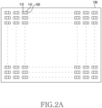
- FIG. 2A is a plan view illustrating the state in which micro-LED chips are attached to a transparent board according to embodiments of the disclosure
- FIG. 2B is a side view illustrating the state in which micro-LED chips are attached to a transparent board according to embodiments of the disclosure.
- a plurality of micro-LED chips 120 is attached in an aligned state on a temporary board by an arrangement device (not illustrated). Each micro-LED chip 120 is maintained in the state of being attached to one surface of the temporary board.
- An adhesive for example, an adhesive layer (e.g., the adhesive layer 122 in FIG. 5A ), is formed between the micro-LED chip 120 and the temporary board.
- a temporary board 130 (hereinafter, referred to as a second board) is a transparent board, and may be transparent glass including any one of sapphire, alumina, silica, and quartz materials having high transmittance of light in the ultraviolet wavelength band.
- the micro-LED chip 120 is provided in the state of being attached to the second board 130 by an adhesive material such as a polyimide, epoxy, or acrylic material.
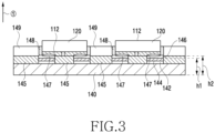
- FIG. 3 is a cross-sectional view illustrating the structure of a micro-LED display according to various embodiments of the disclosure.
- a structure of a micro-LED display (hereinafter, referred to as a display) according to various embodiments of the disclosure will be described with reference to FIG. 3 .
- the display may include a circuit board 140, a first electrode 144, a micro-LED chip 120, a second electrode 112, a bonding structure, and a composite resin part 148.
- the circuit board 140 may be a multilayer printed circuit board 140, and may be formed of any one of ceramic, glass, and polymer materials.
- the circuit board may include a wiring layer 142 and first electrodes 144.
- the circuit board 140 may include a first surface oriented in a first direction and a second surface oriented in a second direction opposite the first direction.
- One or more wiring layers 142 may be formed on the first surface.
- the wiring layers 142 may be signal transmission paths.
- respective wiring layers 142 may be separated from each other by an insulating layer 145.
- the wiring layers 142 may be made of a conductive material.
- the circuit board 140 includes one or more first electrodes 144 formed on one surface of the wiring layer 142.
- the first electrodes 144 may be formed on a surface of the wiring layer 142 oriented in the first direction, and may be configured in pairs. Respective first electrodes 144 may be separated from each other by an insulating layer 145.
- each first electrode 144 may be formed in a layer shape.
- the first electrodes 144 may include a conductive material.
- each first electrode 144 may have a surface layer 146 formed on the first surface oriented in the first direction.
- the surface layer 146 may be a bonding layer that is processed by a laser and bonded to a second electrode 112 of a micro-LED chip 120.
- at least a portion of the surface layer 146 may be bonded to at least a portion of the second electrode 112 so as to produce a thermally reactive layer 147.
- the thermally reactive layer 147 may be a portion of a bonding structure electrically connecting first and second electrodes 144 and 112.
- the thermally reactive layer 147 may be a connection portion electrically connecting first and second electrodes 144 and 112.
- the thermally reactive layer 147 may produce a bonding structure by being produced and then melted through laser treatment.
- the micro-LED chip 120 is arranged on the circuit board 140 in the state of being attached to the second board (e.g., the second board 130 in FIG. 2A ) by an adhesive material (e.g., the adhesive material 122 in FIG. 5A ), and is then bonded to the circuit board 140 by lasers (e.g., a first laser L1 in FIG. 5B and a second laser L2 in FIG. 5D ).
- an adhesive material e.g., the adhesive material 122 in FIG. 5A
- lasers e.g., a first laser L1 in FIG. 5B and a second laser L2 in FIG. 5D .
- the first and second electrodes 140 and 112 are heated by a laser (e.g., the second laser L2 in FIG. 5D ) to produce a bonding structure, such as a thermally reactive layer 147, so that the micro-LED chip 120 can be electrically connected to the wiring layer 142 of the circuit board 140.
- a laser e.g., the second laser L2 in FIG. 5D
- a bonding structure such as a thermally reactive layer 147
- a composite resin part 148 may be agglomerated and cured after being heated by a laser, and may thus be formed in a shape surrounding each micro-LED chip 120.
- the composite resin parts 148 may support respective bonding structures, and each composite resin part 148 may be disposed between a micro-LED chip 120 and the circuit board 140, so that the composite resin part 148 is capable of supporting the bonded micro-LED chips 120 on the circuit board 140.
- the composite resin parts 148 may be disposed on the circuit board 140 at intervals, for example, at equal intervals. Since the micro-LED chips 120 are disposed on the circuit board 140 at equal intervals, the composite resin parts 148 may also be disposed on the circuit board 140 at equal intervals.
- each composite resin parts 1480 may close a second electrode 112 of a bonding structure from the outside. Accordingly, each composite resin part 1480 may be a protective structure having a bonding structure.
- the final height h1 of the first electrodes 144 of the circuit board 140 may be lower than or equal to the final height h2 of the insulating layer 145. This structure may help implementing a flat composite resin layer 1480.
- Empty spaces 149 may exist between respective composite resin parts 148.
- the empty spaces 149 may be formed between the micro-LED chips 120, and may be disposed at equal intervals.
- FIG. 4 is a flowchart sequentially illustrating a process of manufacturing a micro-LED display according to the embodiments of the disclosure.
- FIGS. 5A to 5D are cross-sectional views sequentially illustrating a process of manufacturing a micro-LED display according to the embodiments of the disclosure.
- FIG. 4 A process of manufacturing a micro-LED display according to the embodiments of the disclosure will be described with reference to FIG. 4 and FIGS. 5A to 5D .
- a composite resin layer 1480 is coated on a circuit board 140 (e.g., operation 401 in FIG. 4 ).
- the circuit board 140 may be a board that receives a micro-LED chip 120 in one-to-one correspondence so that the micro-LED chip 120 can be mounted on the circuit board 140.
- the circuit board 140 may include a TFT board.
- the composite resin layer may be a layer having a viscosity of a predetermined level or higher, and may be applied to the board.
- the composite resin layer 1480 may be made of a composite material including, for example, a polymer resin such as epoxy or acrylic and a flux.
- the composite resin layer 1480 may include a sticky mixture composed of an adhesive material and a flux.
- the composite resin layer may be made of two or more materials having different boiling points and have the following features: while being coated, the materials have a viscosity between about 500 CPA and about 1500 CPS due to two solvents, and after being coated, the viscosity of the materials increase since the solvent having a lower boiling point is vaporized, and the materials sufficiently absorb an impact applied when the micro-LED chips 120 are jetted and seated.
- the composite resin layer 1480 may be a damping layer applied on the circuit board 140 to absorb an impact caused by a collision with a jetted micro-LED chip 120, and may be an adhesive layer 122 that causes the micro-LED chip 120 to be fixed at a predetermined position.
- the composite resin layer 1480 is capable of absorbing, from the transparent board, an impact of the micro-LED chip 120 bumping thereinto with acceleration, and is capable of helping the micro-LED chip 120 to be seated on a target first electrode 144 of circuit board 140.
- the composite resin layer 1480 may have a melting point of about 300 degrees C or lower, and may contain solder particles having a diameter of 0.01 mm or less.
- solder may include any one or more of tin, silver, copper, indium, zinc, bismuth, and gold.
- the micro-LED chip 120 is prepared in the state of being attached to the second board 130 by adhesive 122 (e.g., operation 403 in FIG. 4 ). After the micro-LED chips 120 are attached to the second board 130, the pads 112 are aligned on the circuit board 140 in a pad-down state (e.g., operation 405 in FIG. 4 ). In this case, one micro-LED chip 120 may face first electrodes 144 of one circuit board 140 in one-to-one correspondence. Operation 401 may be performed after operation 403.
- the first laser L1 irradiates the micro-LED chip 120 with laser light, preferably from above the top surface of the micro-LED chip 120. Since the board is a transparent material, the laser light that has passed through the board is capable of ablating the adhesive 122 (e.g., operation 407 in FIG. 4 ).
- the first laser L1 may include a laser having an ultraviolet wavelength band having excellent optical transmittance or a pulse wave writing device.
- the first laser L1 has a wavelength of 400 nm or less and a pulse frequency of 1HZ or less, and one or more micro-LED chips 120 may fall on the composite resin layer 1480 of the circuit board 140 in one shot.
- each micro-LED chip 120 falls on the composite resin layer 1480 in the state of having acceleration. This state may be referred to as jetting of the micro-LED 120. In this operation, the laser light from the first laser L1 and the micro-LED chip 120 may proceed simultaneously.
- the composite resin layer 1480 absorbs the impact of a micro-LED chip 120 bumping thereinto thanks to the cushioning action and adhesive property thereof, and accordingly, the micro-LED chip 120 is seated on the target electrodes (e.g., operation 409 in FIG. 4 ).
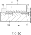
- Each micro-LED chip 120 seated on the composite resin layer 1480 is illustrated in FIG. 5C .
- the second electrodes 112 of each of the seated micro-LED chips 120 is in the state of facing the first electrodes 144 of the circuit board 140. Between the first electrodes 144 and the second electrodes 112, a portion of a relatively thin composite resin layer 1480a may exist, and a surface layer 146 may exist.
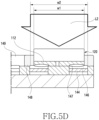
- a second laser L2 irradiates the LED chip 120 seated on the composite resin layer 1480 with laser light, preferably from above the top surface of the micro-LED chip 120 seated on the composite resin layer 1480.
- a heating operation e.g., to about 120 degrees C or higher
- the first electrodes 144 and the second electrodes 112 are bonded to each other (e.g., operation 411 in FIG. 4 ).
- the composite resin layer undergoes phase decomposition into flux and adhesive.
- the flux is capable of improving the wetting property of the bonding portion so as to achieve smooth solder bonding, and the adhesive is coated on the bonding portion so as to protect the bonding portion.
- solder may be included in the composite resin layer 1480, may be included in the surface layer 146, or may be included in both of the composite resin layer 1480 and the surface layer 146.
- the composite resin layer 1480 may include particles of, for example, a white or black color. Due to the inclusion of these particles, the composite resin layer 1480 may improve optical properties of the display.
- the second laser L2 radiates laser light toward the second electrodes 112, the second electrodes 112 and the surface layer 146 are melted, so that chemical bonding may be achieved.
- the thermal reactive layer 147 may be produced through such chemical bonding.
- the thermally reactive layer 147 may be a portion of a bonding structure electrically connecting first and second electrodes 144 and 112.
- the second laser L2 may be a laser of an infrared wavelength band.
- the second laser may be configured to radiate laser light having a width equal to or slightly larger than the width of the first electrodes 144.
- the second laser may be configured to radiate laser light having a width equal to or slightly larger than the width of the second electrodes 112.
- the composite resin layer 1480 which has been present, is agglomerated and cured by irradiation by the second laser L2, and may serve as a support member for supporting the bonding structure between the circuit board 140 and a micro-LED chip 120.
- the cured composite resin layer 1480 will be referred to as a composite resin part 148.
- the composite resin part 148 may be formed to surround a micro-LED chip 120 on the circuit board 140.
- the composite resin part 148 may be formed to surround a bonding structure.
- One micro-LED chip 120 may have one composite resin part 148 formed thereon. Respective micro-LED chips 120 may be spaced apart from each other, and an empty space 149 may exist between respective composite resin parts 148
- FIG. 6A is a plan view illustrating the state in which a micro-LED chip is connected to first electrodes
- FIG. 6B is a vertical cross-sectional view illustrating the state in which a micro-LED chip is connected to first electrodes.
- the size of the micro-LED chip (C x C') may be made to be smaller than the size of the first electrodes 144 (D x D').
- a distance B between one end of an first electrode 144 in a place in which the first electrodes face each other and one end of a second end 112 in a place in which the second electrodes face each other may be designed to be smaller than a distance A between the other end of the first electrode 144 and the other end of the second electrode 112 at the other sides.
- the second electrodes 112 of the micro-LED chip may be formed to be smaller than the size of the first electrodes 144 of the circuit board.
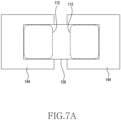
- FIG. 7A is a plan view illustrating the state in which a micro-LED chip is connected to first electrodes.
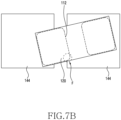
- FIG. 7B is a plan view illustrating the state in which a micro-LED is incorrectly connected to first electrodes.
- FIG. 7A illustrates a case where the second electrodes 112 of each micro-LED chip are aligned on the first electrodes 144 of each circuit board 140 on one-to-one (1:1) correspondence and then correctly seated.
- the first electrodes 144 or the second electrodes 112 may be formed in a rectangular shape.
- the first electrodes 144 may have various shapes as necessary.
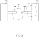
- FIG. 8 is a plan view illustrating a shape of first electrodes.
- the area of the first portions 144a may be smaller or narrower than the area of the second portions 144b.
- the first portions 144a may extend toward each other from the second portions 144b, respectively, and have a rectangular shape that is narrower than the vertical width of the second portions 144b.
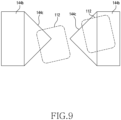
- FIG. 9 is a plan view illustrating another shape of first electrodes.
- each the first portions 144c may be formed in a triangular shape having a bottom side, which corresponds to the vertical width of a corresponding one of the second portions 144d.
- a micro-LED display 1000 manufactured through the manufacturing process illustrated in FIGS. 5A to 5D is illustrated in FIG. 10 .
- a plurality of pixels P may be disposed at a predetermined interval, and each pixel may include sub-pixels Pr, Pg, and Pb.
- micro-LED chips e.g., micro-LED chips 120 in FIG. 3
- a circuit board e.g., the circuit board 140 in FIG. 3A
Landscapes
- Led Device Packages (AREA)
Description
- Various embodiments of the disclosure relate to a multi-transfer technology of a micro-LED chip.
- There is technology for making, as a new display, a display panel by mounting LEDs emitting R (red), G (green), and B (blue) colors on a circuit board.
- However, in order to implement a display, the development of a micro-LEDs (µLEDs) that are capable of corresponding to current pixels must be preceded. Further, it is necessary to solve in advance the problem of how to pick up micro-LED chips of several tens of µm in size and place the chips on a circuit board precisely, and the problem of how to arrange input/output terminals and electrically connect the terminals to a main printed circuit board.
- Conventionally, a method using a dedicated chip-bonding device has been performed, in which a LED chip is picked up by vacuum suction using a finely processed nozzle and is then put down to be in one-to-one correspondence with a desired electrode on a circuit board, and then the nozzle moves away therefrom.
-
US 2017/365588 A1 discloses an optoelectronic semiconductor device that includes an epitaxial substrate and a plurality of microsized optoelectronic semiconductor elements. The microsized optoelectronic semiconductor elements are disposed separately and disposed on a surface of the epitaxial substrate. A length of a side of each of the microsized optoelectronic semiconductor elements is between 1 micrometer and 100 micrometers, and a minimum interval between two adjacent microsized optoelectronic semiconductor elements is 1 micrometer. -
US 2017/263593 A1 discloses another conventional transfer method. - However, the conventional method in which one nozzle picks up and places one individual chip has problems in that it takes a lot of time to mount a plurality of LED chips on a board at high speed, and that price increases and equipment is complicated due to installation of a number of nozzle units.
- In addition, due to the limitation of nozzle processing, there is a technical limitation in transferring micro-LEDs of 100 microns or less.
- According to various embodiments of the disclosure, it is possible to provide a method of manufacturing a micro-LED display with a high-speed transfer method.
- According to various embodiments of the disclosure, it is possible to provide a manufacturing method, in which a composite resin layer having an adhesive property that absorbs an impact applied from a micro-LED chip due to an impact of gas plumes generated during ablation is used, whereby transfer yield is improved.
- According to various embodiments of the disclosure, it is possible to provide a method of manufacturing a micro-LED display, in which in order to improve the precision in seating position of a micro-LED chip, a composite agent composed of a flux and an epoxy (or acrylic) adhesive is coated on a target board to which the micro-LED chip is transferred so as to reduce an impact applied when the micro-LED chip falls down, whereby a transfer yield is improved.
- According to various embodiments of the disclosure, it is possible to provide a method of manufacturing a micro-LED display, in which the shape of electrodes of a circuit board is changed in order to minimize occurrence of defects due to misalignment of a micro-LED chip in the X and Y direction or in particular, due to tilting of the micro-LED chip during the transfer of the micro-LED chip.
- According to the disclosure, a micro-LED display may include: a circuit board; at least one first electrode provided on the circuit board; at least one micro-LED chip bonded onto the first electrode; a second electrode provided on the micro-LED chip; a bonding structure formed by heating the first electrode and the second electrode through laser irradiation; and at least one composite resin part supporting the bonding structure.
- According to an embodiment of the invention, a method of manufacturing a micro-LED display includes: a first step for forming a composite resin layer on a circuit board; a second step for aligning a transparent board to which a plurality of micro-LED chips are attached via adhesive on the first board; a third step of ablating the adhesive by irradiating each of the micro-LED chips with at least one first laser beam; a fourth step of jetting the micro-LED chips to be seated on the composite resin layer; a fifth step of irradiating electrodes of the seated micro-LED chips with at least one second laser beam; and a sixth step of bonding electrodes of the circuit board and the electrodes of the micro LED chips by means of said irradiating with the at least one second laser beam.
- The disclosure enables multi-transfer of micro LED chips using a LASER ablation method at high speed, thereby improving productivity.
- In addition, the disclosure is capable of improving the transfer yield of micro LED chips.
-
-
FIG. 1A is a view illustrating the configuration of a base board for manufacturing micro-LED chips in a pad-up state according to various embodiments of the disclosure. -
FIG. 1B is a view illustrating the configuration of a base board for manufacturing micro-LED chips in a pad-down state according to various embodiments of the disclosure. -
FIG. 1C is a view illustrating a configuration of a micro-LED chip according to various embodiments of the disclosure. -
FIG. 2A is a plan view illustrating the state in which micro-LED chips are attached to a transparent board according to various embodiments of the disclosure, andFIG. 2B is a side view illustrating the state in which micro-LED chips are attached to a transparent board according to various embodiments of the disclosure. -
FIG. 3 is a cross-sectional view illustrating the structure of a micro-LED display according to various embodiments of the disclosure. -
FIG. 4 is a flowchart sequentially illustrating a process of manufacturing a micro-LED display according to various embodiments of the disclosure. -
FIGS. 5A to 5D are cross-sectional views sequentially illustrating a process of manufacturing a micro-LED display according to various embodiments of the disclosure. -
FIG. 6A is a plan view illustrating the state in which a micro-LED chip according to various embodiments of the disclosure is connected to first electrodes, andFIG. 6B is a vertical cross-sectional view illustrating the state in which a micro-LED chip according to various embodiments of the disclosure is connected to first electrodes. -
FIG. 7A is a plan view illustrating the state in which a micro-LED chip according to various embodiments of the disclosure is connected to first electrodes. -
FIG. 7B is a plan view illustrating the state in which a micro-LED chip according to various embodiments of the disclosure is incorrectly connected to first electrodes. -
FIG. 8 is a plan view illustrating a shape of first electrodes according to various embodiments of the disclosure. -
FIG. 9 is a plan view illustrating another shape of first electrodes according to various embodiments of the disclosure. -
FIG. 10 is a plan view illustrating a micro-LED display manufactured according to various embodiments of the disclosure. - Hereinafter, various embodiments of the disclosure will be described with reference to the accompanying drawings. However, it shall be understood that it is not intended to limit the disclosure to specific embodiments, and that the disclosure includes various modifications, equivalents, and/or alternatives of embodiments of the disclosure. In connection with the description of drawings, similar components may be denoted by similar reference numerals.
- Hereinafter, with reference to the accompanying drawings, a structure of a display and a method of manufacturing the display using a micro-LED mounting technology according to various embodiments of the disclosure will be described. It is to be understood that the present invention relates to a manufacturing method. The described micro-LED chips, micro-LED displays, and intermediate structures obtained at different stages of the manufacturing method, are useful to understand the invention but do not form part of the invention per se, even when they are referred to as "embodiments".
- Since the configuration of the display according to an exemplary embodiment of the disclosure is capable of being implemented regardless of the size of an LED, the size of a used LED is not limited. For example, a lighting display uses several-mm-class LEDs, a large display such as an indoor/outdoor signage use hundreds-of-pm-class LEDs, and several-µm-class to tens-of-pm-class LEDs may be used for a display.
- In the exemplary embodiments of the disclosure, a transfer device and method for a micro-LED chip are illustrated and described.
-
FIG. 1A is a view illustrating the configuration of a base board for manufacturing micro-LED chips in a pad-up state according to various embodiments of the disclosure.FIG. 1A is a view illustrating the configuration of a base board for manufacturing micro-LED chips in a pad-down state according to various embodiments of the disclosure. - Referring to
FIGS. 1A and1B , amicro-LED chip 110 may have a size of several tens of µm (e.g., 30 to 40 µm) so as to be applied to a sub-pixel constituting a pixel of a near-field display. A plurality of micro-LEDs 110 may be grown in a single crystal state of a compound semiconductor in a high-temperature/high-pressure state on a sapphire-, GaAs-, or SiX-based base board 100 (e.g., a wafer), and colors (e.g., red, green, and blue) may be configured differently depending on respective compositions. For example, red is composed of a GaAs compound semiconductor, green is composed of an InGaP compound semiconductor, and blue is composed of a GaN compound semiconductor. Wavelengths are determined depending on intrinsic energy bandgap values of respective compositions, and thus colors to be implemented are different from each other. - According to an embodiment, in order for a grown micro-LED 110 to emit light, a semiconductor process having several tens of steps may be performed to obtain an electrically connectable structure, which is capable of supplying holes and electrons. In this case, a pair of
connection pads 112 disposed to protrude from a micro-LED 110 may be fabricated in a form facing upward (pad-up) (seeFIG. 1A ) or a form facing downward (pad-down) (seeFIG. 1B ) with respect to abase board 100. -
FIG. 1C is a view illustrating a configuration of a micro-LED chip according to various embodiments of the disclosure. - Referring to
FIG. 1C , each micro-LED obtained after cutting micro-LEDs may be referred to as a micro-LED chip. Eachmicro-LED chip 120 includes abody 111 as a light-emitting portion and a pair ofconnection pads 112 protruding from thebody 111 at a predetermined interval. According to an embodiment, themicro-LED chip 110 may be electrically connected to a board (PCB) of an electronic device (e.g., a display) using a conveyance device according to the disclosure to be described later. Hereinafter, theconnection pads 112 of themicro-LED chip 120 will be referred to as second electrodes. -
FIG. 2A is a plan view illustrating the state in which micro-LED chips are attached to a transparent board according to embodiments of the disclosure, andFIG. 2B is a side view illustrating the state in which micro-LED chips are attached to a transparent board according to embodiments of the disclosure. - Referring to
FIGS. 2A and2B , a plurality ofmicro-LED chips 120 is attached in an aligned state on a temporary board by an arrangement device (not illustrated). Eachmicro-LED chip 120 is maintained in the state of being attached to one surface of the temporary board. An adhesive, for example, an adhesive layer (e.g., theadhesive layer 122 inFIG. 5A ), is formed between themicro-LED chip 120 and the temporary board. - According to the embodiments, a temporary board 130 (hereinafter, referred to as a second board) is a transparent board, and may be transparent glass including any one of sapphire, alumina, silica, and quartz materials having high transmittance of light in the ultraviolet wavelength band. The
micro-LED chip 120 is provided in the state of being attached to thesecond board 130 by an adhesive material such as a polyimide, epoxy, or acrylic material. -
FIG. 3 is a cross-sectional view illustrating the structure of a micro-LED display according to various embodiments of the disclosure. - A structure of a micro-LED display (hereinafter, referred to as a display) according to various embodiments of the disclosure will be described with reference to
FIG. 3 . - According to various embodiments, the display may include a
circuit board 140, afirst electrode 144, amicro-LED chip 120, asecond electrode 112, a bonding structure, and acomposite resin part 148. - According to various embodiments, the
circuit board 140 may be a multilayer printedcircuit board 140, and may be formed of any one of ceramic, glass, and polymer materials. The circuit board may include awiring layer 142 andfirst electrodes 144. Thecircuit board 140 may include a first surface oriented in a first direction and a second surface oriented in a second direction opposite the first direction. One ormore wiring layers 142 may be formed on the first surface. The wiring layers 142 may be signal transmission paths. For example, respective wiring layers 142 may be separated from each other by an insulatinglayer 145. The wiring layers 142 may be made of a conductive material. - According to the embodiments, the
circuit board 140 includes one or morefirst electrodes 144 formed on one surface of thewiring layer 142. Thefirst electrodes 144 may be formed on a surface of thewiring layer 142 oriented in the first direction, and may be configured in pairs. Respectivefirst electrodes 144 may be separated from each other by an insulatinglayer 145. For example, eachfirst electrode 144 may be formed in a layer shape. Thefirst electrodes 144 may include a conductive material. - In various embodiments, each
first electrode 144 may have asurface layer 146 formed on the first surface oriented in the first direction. Thesurface layer 146 may be a bonding layer that is processed by a laser and bonded to asecond electrode 112 of amicro-LED chip 120. For example, at least a portion of thesurface layer 146 may be bonded to at least a portion of thesecond electrode 112 so as to produce a thermallyreactive layer 147. The thermallyreactive layer 147 may be a portion of a bonding structure electrically connecting first andsecond electrodes - According to various embodiments, the thermally
reactive layer 147 may be a connection portion electrically connecting first andsecond electrodes reactive layer 147 may produce a bonding structure by being produced and then melted through laser treatment. - According to the embodiments, the
micro-LED chip 120 is arranged on thecircuit board 140 in the state of being attached to the second board (e.g., thesecond board 130 inFIG. 2A ) by an adhesive material (e.g., theadhesive material 122 inFIG. 5A ), and is then bonded to thecircuit board 140 by lasers (e.g., a first laser L1 inFIG. 5B and a second laser L2 inFIG. 5D ). - The first and
second electrodes FIG. 5D ) to produce a bonding structure, such as a thermallyreactive layer 147, so that themicro-LED chip 120 can be electrically connected to thewiring layer 142 of thecircuit board 140. - According to various embodiments, a
composite resin part 148 may be agglomerated and cured after being heated by a laser, and may thus be formed in a shape surrounding eachmicro-LED chip 120. Thecomposite resin parts 148 may support respective bonding structures, and eachcomposite resin part 148 may be disposed between amicro-LED chip 120 and thecircuit board 140, so that thecomposite resin part 148 is capable of supporting the bondedmicro-LED chips 120 on thecircuit board 140. - According to various embodiments, the
composite resin parts 148 may be disposed on thecircuit board 140 at intervals, for example, at equal intervals. Since themicro-LED chips 120 are disposed on thecircuit board 140 at equal intervals, thecomposite resin parts 148 may also be disposed on thecircuit board 140 at equal intervals. For example, eachcomposite resin parts 1480 may close asecond electrode 112 of a bonding structure from the outside. Accordingly, eachcomposite resin part 1480 may be a protective structure having a bonding structure. - In the display according to various embodiments, the final height h1 of the
first electrodes 144 of thecircuit board 140 may be lower than or equal to the final height h2 of the insulatinglayer 145. This structure may help implementing a flatcomposite resin layer 1480. -
Empty spaces 149 may exist between respectivecomposite resin parts 148. Theempty spaces 149 may be formed between themicro-LED chips 120, and may be disposed at equal intervals. -
FIG. 4 is a flowchart sequentially illustrating a process of manufacturing a micro-LED display according to the embodiments of the disclosure.FIGS. 5A to 5D are cross-sectional views sequentially illustrating a process of manufacturing a micro-LED display according to the embodiments of the disclosure. - A process of manufacturing a micro-LED display according to the embodiments of the disclosure will be described with reference to
FIG. 4 andFIGS. 5A to 5D . - Referring to
FIG. 5A , in a display, acomposite resin layer 1480 is coated on a circuit board 140 (e.g.,operation 401 inFIG. 4 ). Thecircuit board 140 may be a board that receives amicro-LED chip 120 in one-to-one correspondence so that themicro-LED chip 120 can be mounted on thecircuit board 140. For example, thecircuit board 140 may include a TFT board. - According to various embodiments, the composite resin layer may be a layer having a viscosity of a predetermined level or higher, and may be applied to the board. For example, the
composite resin layer 1480 may be made of a composite material including, for example, a polymer resin such as epoxy or acrylic and a flux. Thecomposite resin layer 1480 may include a sticky mixture composed of an adhesive material and a flux. - According to various embodiments, the composite resin layer may be made of two or more materials having different boiling points and have the following features: while being coated, the materials have a viscosity between about 500 CPA and about 1500 CPS due to two solvents, and after being coated, the viscosity of the materials increase since the solvent having a lower boiling point is vaporized, and the materials sufficiently absorb an impact applied when the
micro-LED chips 120 are jetted and seated. Thecomposite resin layer 1480 may be a damping layer applied on thecircuit board 140 to absorb an impact caused by a collision with a jettedmicro-LED chip 120, and may be anadhesive layer 122 that causes themicro-LED chip 120 to be fixed at a predetermined position. Due to a damping action, that is, a cushion-like action, and due to an adhesive property, thecomposite resin layer 1480 is capable of absorbing, from the transparent board, an impact of themicro-LED chip 120 bumping thereinto with acceleration, and is capable of helping themicro-LED chip 120 to be seated on a targetfirst electrode 144 ofcircuit board 140. - According to various embodiments, the
composite resin layer 1480 may have a melting point of about 300 degrees C or lower, and may contain solder particles having a diameter of 0.01 mm or less. When thecomposite resin layer 1480 is heated, solder is melted and thefirst electrodes 144 on thecircuit board 140 and thesecond electrodes 122 on themicro-LED chip 120 can be bonded to each other. For example, the solder may include any one or more of tin, silver, copper, indium, zinc, bismuth, and gold. - According to the invention, the
micro-LED chip 120 is prepared in the state of being attached to thesecond board 130 by adhesive 122 (e.g.,operation 403 inFIG. 4 ). After themicro-LED chips 120 are attached to thesecond board 130, thepads 112 are aligned on thecircuit board 140 in a pad-down state (e.g.,operation 405 inFIG. 4 ). In this case, onemicro-LED chip 120 may facefirst electrodes 144 of onecircuit board 140 in one-to-one correspondence.Operation 401 may be performed afteroperation 403. - Referring to
FIG. 5B , in the display, the first laser L1 irradiates themicro-LED chip 120 with laser light, preferably from above the top surface of themicro-LED chip 120. Since the board is a transparent material, the laser light that has passed through the board is capable of ablating the adhesive 122 (e.g.,operation 407 inFIG. 4 ). For example, the first laser L1 may include a laser having an ultraviolet wavelength band having excellent optical transmittance or a pulse wave writing device. In addition, the first laser L1 has a wavelength of 400 nm or less and a pulse frequency of 1HZ or less, and one or moremicro-LED chips 120 may fall on thecomposite resin layer 1480 of thecircuit board 140 in one shot. - Due to the ablation phenomenon of the adhesive 122, each
micro-LED chip 120 falls on thecomposite resin layer 1480 in the state of having acceleration. This state may be referred to as jetting of themicro-LED 120. In this operation, the laser light from the first laser L1 and themicro-LED chip 120 may proceed simultaneously. - After jetting each
micro-LED chip 120, thecomposite resin layer 1480 absorbs the impact of amicro-LED chip 120 bumping thereinto thanks to the cushioning action and adhesive property thereof, and accordingly, themicro-LED chip 120 is seated on the target electrodes (e.g.,operation 409 inFIG. 4 ). Eachmicro-LED chip 120 seated on thecomposite resin layer 1480 is illustrated inFIG. 5C . - Referring to
FIG. 5C , thesecond electrodes 112 of each of the seatedmicro-LED chips 120 is in the state of facing thefirst electrodes 144 of thecircuit board 140. Between thefirst electrodes 144 and thesecond electrodes 112, a portion of a relatively thincomposite resin layer 1480a may exist, and asurface layer 146 may exist. - Referring to
FIG. 5D , in the display according to various embodiments, a second laser L2 irradiates theLED chip 120 seated on thecomposite resin layer 1480 with laser light, preferably from above the top surface of themicro-LED chip 120 seated on thecomposite resin layer 1480. In a heating operation (e.g., to about 120 degrees C or higher) by irradiation of the second laser L2, thefirst electrodes 144 and thesecond electrodes 112 are bonded to each other (e.g.,operation 411 inFIG. 4 ). By this heating operation, the composite resin layer undergoes phase decomposition into flux and adhesive. Thus, the flux is capable of improving the wetting property of the bonding portion so as to achieve smooth solder bonding, and the adhesive is coated on the bonding portion so as to protect the bonding portion. - Meanwhile, solder may be included in the
composite resin layer 1480, may be included in thesurface layer 146, or may be included in both of thecomposite resin layer 1480 and thesurface layer 146. - According to various embodiments, the
composite resin layer 1480 may include particles of, for example, a white or black color. Due to the inclusion of these particles, thecomposite resin layer 1480 may improve optical properties of the display. - When the second laser L2 radiates laser light toward the
second electrodes 112, thesecond electrodes 112 and thesurface layer 146 are melted, so that chemical bonding may be achieved. The thermalreactive layer 147 may be produced through such chemical bonding. The thermallyreactive layer 147 may be a portion of a bonding structure electrically connecting first andsecond electrodes first electrodes 144. Alternatively, the second laser may be configured to radiate laser light having a width equal to or slightly larger than the width of thesecond electrodes 112. - In the display, the
composite resin layer 1480, which has been present, is agglomerated and cured by irradiation by the second laser L2, and may serve as a support member for supporting the bonding structure between thecircuit board 140 and amicro-LED chip 120. The curedcomposite resin layer 1480 will be referred to as acomposite resin part 148. Thecomposite resin part 148 may be formed to surround amicro-LED chip 120 on thecircuit board 140. In addition, thecomposite resin part 148 may be formed to surround a bonding structure. Onemicro-LED chip 120 may have onecomposite resin part 148 formed thereon. Respectivemicro-LED chips 120 may be spaced apart from each other, and anempty space 149 may exist between respectivecomposite resin parts 148 -
FIG. 6A is a plan view illustrating the state in which a micro-LED chip is connected to first electrodes, andFIG. 6B is a vertical cross-sectional view illustrating the state in which a micro-LED chip is connected to first electrodes. - Referring to
FIGS. 6A and 6B , in the display, in order to heat electrodes by partially irradiating the display with laser light or an energy beam, the size of the micro-LED chip (C x C') may be made to be smaller than the size of the first electrodes 144 (D x D'). - In the display, in order to prevent a short circuit, a distance B between one end of an
first electrode 144 in a place in which the first electrodes face each other and one end of asecond end 112 in a place in which the second electrodes face each other may be designed to be smaller than a distance A between the other end of thefirst electrode 144 and the other end of thesecond electrode 112 at the other sides. - According to various embodiments, the
second electrodes 112 of the micro-LED chip may be formed to be smaller than the size of thefirst electrodes 144 of the circuit board. -
FIG. 7A is a plan view illustrating the state in which a micro-LED chip is connected to first electrodes.FIG. 7B is a plan view illustrating the state in which a micro-LED is incorrectly connected to first electrodes. -
FIG. 7A illustrates a case where thesecond electrodes 112 of each micro-LED chip are aligned on thefirst electrodes 144 of eachcircuit board 140 on one-to-one (1:1) correspondence and then correctly seated. In general, thefirst electrodes 144 or thesecond electrodes 112 may be formed in a rectangular shape. - However, as illustrated in
FIG. 7B , when asecond electrode 112 of themicro-LED chip 120 are connected to an electrode on the opposite side, an electrical short portion/an open defect F may occur in an electronic circuit. In order to prevent such a defective connection state, thefirst electrodes 144 may have various shapes as necessary. -
FIG. 8 is a plan view illustrating a shape of first electrodes. - Referring to
FIG. 8 , in thefirst electrodes 144, assuming that, with respect to the intermediate portion, portions located near each other arefirst portions 144a and portions located far from each other aresecond portions 144b, the area of thefirst portions 144a may be smaller or narrower than the area of thesecond portions 144b. For example, thefirst portions 144a may extend toward each other from thesecond portions 144b, respectively, and have a rectangular shape that is narrower than the vertical width of thesecond portions 144b. -
FIG. 9 is a plan view illustrating another shape of first electrodes. - Referring to
FIG. 9 , in thefirst electrodes 144, assuming that, with respect to the intermediate portion, portions located near each other arefirst portions 144c and portions located far from each other are second portions 144d, the area of thefirst portions 144c may be smaller or narrower than the area of the second portions 144d. For example, each thefirst portions 144c may be formed in a triangular shape having a bottom side, which corresponds to the vertical width of a corresponding one of the second portions 144d. - A
micro-LED display 1000 manufactured through the manufacturing process illustrated inFIGS. 5A to 5D is illustrated inFIG. 10 . - According to an embodiment, in the
display 1000, a plurality of pixels P may be disposed at a predetermined interval, and each pixel may include sub-pixels Pr, Pg, and Pb. According to an embodiment, micro-LED chips (e.g.,micro-LED chips 120 inFIG. 3 ) corresponding to respective sub-pixels Pr, Pg, and Pb can be mounted on a circuit board (e.g., thecircuit board 140 in FIG. 3A) of thedisplay 100 be quickly and accurately. - Various embodiments disclosed in this specification and the drawings are provided merely to represent specific examples for the purpose of easily describing the technical contents of the disclosure and helping the understanding of the disclosure, and are not intended to limit the scope of the disclosure. Accordingly, the scope of the disclosure should be construed in such a manner that, in addition to the embodiments disclosed herein, all changes or modifications derived from the technical idea of the disclosure are included in the scope of the disclosure. The invention is defined by the appended claims.
Claims (9)
- A method of manufacturing a micro-LED display, the method comprising the following successive steps:a first step (401) for forming a composite resin layer (1480) on a circuit board (140);a second step (405) for aligning a transparent board (130) to which a plurality of micro-LED chips (120) are attached (403) via adhesive (122) on the first circuit board (140);a third step (407) of ablating the adhesive (122) by irradiating each of the micro-LED chips (120) with at least one first laser beam (L1);a fourth step (409) of jetting the micro-LED chips (120) to be seated on the composite resin layer (1480);a fifth step of irradiating electrodes (112) of the seated micro-LED chips (120) with at least one second laser beam (L2); anda sixth step (411) of bonding electrodes (144) of the circuit board (140) and the electrodes (112) of the micro LED chips (120) by means of said irradiating with the at least one second laser beam (L2).
- The method of claim 1, wherein after the sixth step (411), the composite resin layer (1480) is cured and encloses a bonded state of the micro-LED chips (120).
- The method of claim 1, wherein the electrodes (112) of the micro-LED chips (120) have a size smaller than a size of the electrodes (144) of the board (140).
- The method of claim 1, wherein the composite resin layer (1480) is uniformly coated on the electrodes (144) of the circuit board (140) to a thickness of 0.015 mm or less.
- The method of claim 1, wherein the composite resin layer (1480) acts as a damping layer that absorbs an impact of jetted micro LED chips (120), and is made of a material having an adhesive property to cause the seated micro LED chips (120) to be attached thereto.
- The method of claim 1, wherein the composite resin layer (1480) is composed of two or more solvent materials having different boiling points, wherein in the first step, the composite resin layer (1480) has a viscosity of 1,000 CPS or less by two solvents, and after the first step, a solvent having a lower boiling point is evaporated and the viscosity increases.
- The method of claim 1, wherein the composite resin layer (1480) contains solder particles having a melting point of 300 degrees C or lower and having a diameter of 0.01 mm or less, and during the sixth step, the solder is melted so that the electrodes (144) of the circuit board (140) and the electrodes (112) of the micro-LED display are bonded to each other.
- The method of claim 1, wherein the composite resin layer (1480) contains white or black particles.
- The method of claim 1, wherein, in the second step, the electrodes (112) of each of the micro LED chips (120) are aligned in a state of facing the electrodes (144) of the circuit board (140) in one-to-one correspondence.
Applications Claiming Priority (2)
| Application Number | Priority Date | Filing Date | Title |
|---|---|---|---|
| KR1020180081682A KR102602393B1 (en) | 2018-07-13 | 2018-07-13 | Micro led display and manufacturing method thereof |
| PCT/KR2019/007564 WO2020013478A1 (en) | 2018-07-13 | 2019-06-24 | Micro-led display and method for manufacturing same |
Publications (3)
| Publication Number | Publication Date |
|---|---|
| EP3823030A1 EP3823030A1 (en) | 2021-05-19 |
| EP3823030A4 EP3823030A4 (en) | 2021-09-08 |
| EP3823030B1 true EP3823030B1 (en) | 2023-05-10 |
Family
ID=69142659
Family Applications (1)
| Application Number | Title | Priority Date | Filing Date |
|---|---|---|---|
| EP19833754.5A Active EP3823030B1 (en) | 2018-07-13 | 2019-06-24 | Method for manufacturing a micro-led display |
Country Status (4)
| Country | Link |
|---|---|
| US (1) | US20210265327A1 (en) |
| EP (1) | EP3823030B1 (en) |
| KR (1) | KR102602393B1 (en) |
| WO (1) | WO2020013478A1 (en) |
Families Citing this family (33)
| Publication number | Priority date | Publication date | Assignee | Title |
|---|---|---|---|---|
| KR20200052044A (en) * | 2018-11-06 | 2020-05-14 | 삼성전자주식회사 | Display apparatus |
| US11255529B1 (en) * | 2019-04-26 | 2022-02-22 | Facebook Technologies, Llc | Bonding corners of light emitting diode chip to substrate using laser |
| KR102862766B1 (en) * | 2019-05-29 | 2025-09-22 | 삼성전자주식회사 | Micro led display and manufacturing method thereof |
| TWI750488B (en) | 2019-07-17 | 2021-12-21 | 錼創顯示科技股份有限公司 | Semiconductor structure and micro semiconductor display device |
| CN110416248B (en) * | 2019-08-06 | 2022-11-04 | 京东方科技集团股份有限公司 | A display substrate, a preparation method thereof, and a display device |
| KR20210019323A (en) | 2019-08-12 | 2021-02-22 | 삼성전자주식회사 | Micro led display and manufacturing method thereof |
| US11127889B2 (en) * | 2019-10-30 | 2021-09-21 | X Display Company Technology Limited | Displays with unpatterned layers of light-absorbing material |
| KR20210106056A (en) * | 2020-02-19 | 2021-08-30 | 한국전자통신연구원 | Transfer and bonding method using laser |
| KR102519953B1 (en) * | 2020-04-13 | 2023-04-11 | 한국전자통신연구원 | Method for transferring and bonding of devices |
| US11677060B2 (en) | 2020-04-13 | 2023-06-13 | Electronics and Teleocmmunications Research Institute | Method for transferring and bonding of devices |
| CN112968105B (en) * | 2020-04-24 | 2021-12-21 | 重庆康佳光电技术研究院有限公司 | Large transfer method for Micro LED chips and display back panel |
| TWI740484B (en) * | 2020-05-04 | 2021-09-21 | 宏碁股份有限公司 | Display device and manufacturing method thereof |
| US20230178686A1 (en) * | 2020-05-14 | 2023-06-08 | Lg Electronics Inc. | Semiconductor light-emitting element and display device including same |
| KR102781957B1 (en) * | 2020-07-07 | 2025-03-18 | 삼성전자주식회사 | Display module and method for manufacturing thereof |
| TWI775111B (en) * | 2020-07-15 | 2022-08-21 | 歆熾電氣技術股份有限公司 | Chip-carrying structure and chip-bonding method |
| CN112885822B (en) | 2020-07-27 | 2023-08-01 | 友达光电股份有限公司 | Manufacturing method of display device |
| WO2022050621A1 (en) * | 2020-09-01 | 2022-03-10 | Samsung Electronics Co., Ltd. | Intermediate structure for manufacturing micro light emitting diode display, method of manufacturing the same, and method of manufacturing micro led display |
| KR102557580B1 (en) * | 2021-01-05 | 2023-07-20 | 엘지전자 주식회사 | Semiconductor light emitting device package and display device |
| TWI753825B (en) * | 2021-05-11 | 2022-01-21 | 財團法人工業技術研究院 | Micro device structure and display apparatus |
| US12349505B2 (en) | 2021-06-01 | 2025-07-01 | Electronics And Telecommunications Research Institute | Method of manufacturing electric device |
| WO2022255504A1 (en) * | 2021-06-01 | 2022-12-08 | 엘지전자 주식회사 | Display device |
| KR20230014983A (en) | 2021-07-22 | 2023-01-31 | 한국전자통신연구원 | Electronic device and its repair method |
| KR102908058B1 (en) * | 2021-09-02 | 2026-01-07 | 엘지전자 주식회사 | Semiconductor light-emitting element for display panel, substrate structure for display panel, and display device including same |
| KR102745496B1 (en) | 2021-11-01 | 2024-12-24 | 엘지전자 주식회사 | Display device |
| WO2023106177A1 (en) * | 2021-12-06 | 2023-06-15 | 東レ株式会社 | Method for manufacturing led-mounting substrate |
| KR20240168915A (en) * | 2022-03-25 | 2024-12-02 | 도레이 카부시키가이샤 | Method for manufacturing an LED mounting substrate having a cured film formed thereon |
| WO2023234435A1 (en) * | 2022-05-31 | 2023-12-07 | 엘지전자 주식회사 | Display device using light emitting elements and manufacturing method therefor |
| WO2024005341A1 (en) * | 2022-06-29 | 2024-01-04 | 삼성전자주식회사 | Connection structure between light emitting diode and substrate, and display module including same |
| WO2024044909A1 (en) * | 2022-08-29 | 2024-03-07 | 天津三安光电有限公司 | Micro light-emitting diode, micro light-emitting element and preparation method therefor, and display |
| KR102913000B1 (en) * | 2022-12-05 | 2026-01-15 | 플레이니트라이드 디스플레이 컴퍼니 리미티드 | Micro element structure and display device |
| WO2024196869A1 (en) * | 2023-03-22 | 2024-09-26 | Applied Materials, Inc. | Direct and selective mass transfer process for microled display fabrication |
| US20250056920A1 (en) * | 2023-08-09 | 2025-02-13 | Applied Materials, Inc. | Die repair process in microled display fabrication |
| TW202539480A (en) * | 2023-10-20 | 2025-10-01 | 美商應用材料股份有限公司 | Releasing separate color conversion layer on micro-led display backplane |
Family Cites Families (21)
| Publication number | Priority date | Publication date | Assignee | Title |
|---|---|---|---|---|
| JP4507358B2 (en) * | 2000-06-16 | 2010-07-21 | 日亜化学工業株式会社 | Optical semiconductor device |
| WO2002084631A1 (en) * | 2001-04-11 | 2002-10-24 | Sony Corporation | Element transfer method, element arrangmenet method using the same, and image display apparatus production method |
| JP4032716B2 (en) * | 2001-11-29 | 2008-01-16 | ソニー株式会社 | Manufacturing method of semiconductor device |
| JP4284911B2 (en) * | 2002-01-09 | 2009-06-24 | ソニー株式会社 | Element transfer method |
| WO2006093264A1 (en) * | 2005-03-04 | 2006-09-08 | Matsushita Electric Industrial Co., Ltd. | Laser heating device and laser heating method |
| KR100638824B1 (en) * | 2005-05-20 | 2006-10-27 | 삼성전기주식회사 | Bonding method of light emitting diode chip |
| JP2010177390A (en) * | 2009-01-29 | 2010-08-12 | Sony Corp | Method of transferring device and method of manufacturing display apparatus |
| KR101622399B1 (en) * | 2009-08-18 | 2016-05-18 | 엘지전자 주식회사 | Led device |
| US8573469B2 (en) * | 2011-11-18 | 2013-11-05 | LuxVue Technology Corporation | Method of forming a micro LED structure and array of micro LED structures with an electrically insulating layer |
| WO2013112435A1 (en) * | 2012-01-24 | 2013-08-01 | Cooledge Lighting Inc. | Light - emitting devices having discrete phosphor chips and fabrication methods |
| US8896010B2 (en) * | 2012-01-24 | 2014-11-25 | Cooledge Lighting Inc. | Wafer-level flip chip device packages and related methods |
| KR20160091526A (en) * | 2015-01-23 | 2016-08-03 | 삼성디스플레이 주식회사 | Method and system for bonding flexible display |
| CN107431107B (en) * | 2015-04-01 | 2020-07-24 | 歌尔股份有限公司 | Micro light emitting diode transfer method, manufacturing method, device and electronic equipment |
| US10319697B2 (en) * | 2015-05-21 | 2019-06-11 | Goertek, Inc. | Transferring method, manufacturing method, device and electronic apparatus of micro-LED |
| CN108352143B (en) * | 2015-09-02 | 2021-04-16 | 脸谱科技有限责任公司 | Assembly of semiconductor devices |
| KR101754528B1 (en) * | 2016-03-23 | 2017-07-06 | 한국광기술원 | Transfer assembly with dry adhesion structure and method for transferring led structure assembly using the same and led structure assembly |
| KR102631260B1 (en) * | 2016-04-08 | 2024-01-31 | 삼성디스플레이 주식회사 | Display apparatus and method thereof |
| TWI685961B (en) * | 2016-06-17 | 2020-02-21 | 優顯科技股份有限公司 | Optoelectronic semiconductor device |
| KR101886085B1 (en) * | 2016-08-30 | 2018-08-07 | 현대자동차 주식회사 | Flux compositon comprising carbon component, solder paste comprising the same and method of soldering |
| KR102688975B1 (en) * | 2016-12-27 | 2024-07-29 | 주식회사 루멘스 | micro LED module and its fabricating method |
| WO2020090684A1 (en) * | 2018-10-31 | 2020-05-07 | デクセリアルズ株式会社 | Method for manufacturing connected body, anisotropic bonding film, and connected body |
-
2018
- 2018-07-13 KR KR1020180081682A patent/KR102602393B1/en active Active
-
2019
- 2019-06-24 EP EP19833754.5A patent/EP3823030B1/en active Active
- 2019-06-24 US US17/253,645 patent/US20210265327A1/en not_active Abandoned
- 2019-06-24 WO PCT/KR2019/007564 patent/WO2020013478A1/en not_active Ceased
Also Published As
| Publication number | Publication date |
|---|---|
| WO2020013478A1 (en) | 2020-01-16 |
| US20210265327A1 (en) | 2021-08-26 |
| KR20200007498A (en) | 2020-01-22 |
| KR102602393B1 (en) | 2023-11-16 |
| EP3823030A4 (en) | 2021-09-08 |
| EP3823030A1 (en) | 2021-05-19 |
Similar Documents
| Publication | Publication Date | Title |
|---|---|---|
| EP3823030A1 (en) | Micro-led display and method for manufacturing same | |
| KR102543408B1 (en) | Light-emitting display unit and display apparatus | |
| US10186549B1 (en) | Gang bonding process for assembling a matrix of light-emitting elements | |
| US12154885B2 (en) | Method and structure for die bonding using energy beam | |
| JP6823893B2 (en) | How to generate a light emitting diode array on the backplane | |
| JP6107060B2 (en) | Method for manufacturing light emitting device | |
| EP2515333A2 (en) | Light Emitting Device Module and Method of Manufacturing the Same | |
| KR20210027848A (en) | Micro led display and manufacturing method thereof | |
| KR20210019323A (en) | Micro led display and manufacturing method thereof | |
| TWI797305B (en) | Led backplane having planar bonding surfaces and method of making thereof | |
| TWI758594B (en) | Transfer substrate, mounting method using the same, and manufacturing method of image display device | |
| US20150200336A1 (en) | Wafer level contact pad standoffs with integrated reflector | |
| JP2024146812A (en) | Method for joining electronic components and method for transporting large quantities of electronic components | |
| US20090207875A1 (en) | Light chip and optical module | |
| CN113196505B (en) | Method for producing an optoelectronic lighting device | |
| KR20200137247A (en) | Micro led display and manufacturing method thereof | |
| KR102121407B1 (en) | Method for transferring semiconductor light emitting device | |
| US11588084B2 (en) | Method and structure for die bonding using energy beam | |
| US20240282885A1 (en) | Display module, fabrication method and repair method thereof | |
| TWI923914B (en) | Method and structure for die bonding using energy beam | |
| KR20200088933A (en) | Apparatus for transferring semiconductor light emitting device |
Legal Events
| Date | Code | Title | Description |
|---|---|---|---|
| STAA | Information on the status of an ep patent application or granted ep patent |
Free format text: STATUS: THE INTERNATIONAL PUBLICATION HAS BEEN MADE |
|
| PUAI | Public reference made under article 153(3) epc to a published international application that has entered the european phase |
Free format text: ORIGINAL CODE: 0009012 |
|
| STAA | Information on the status of an ep patent application or granted ep patent |
Free format text: STATUS: REQUEST FOR EXAMINATION WAS MADE |
|
| 17P | Request for examination filed |
Effective date: 20210211 |
|
| AK | Designated contracting states |
Kind code of ref document: A1 Designated state(s): AL AT BE BG CH CY CZ DE DK EE ES FI FR GB GR HR HU IE IS IT LI LT LU LV MC MK MT NL NO PL PT RO RS SE SI SK SM TR |
|
| A4 | Supplementary search report drawn up and despatched |
Effective date: 20210811 |
|
| RIC1 | Information provided on ipc code assigned before grant |
Ipc: H01L 25/075 20060101ALI20210805BHEP Ipc: H01L 33/56 20100101ALI20210805BHEP Ipc: H01L 33/54 20100101ALI20210805BHEP Ipc: H01L 33/62 20100101ALI20210805BHEP Ipc: H01L 33/38 20100101ALI20210805BHEP Ipc: H01L 27/15 20060101AFI20210805BHEP |
|
| DAV | Request for validation of the european patent (deleted) | ||
| DAX | Request for extension of the european patent (deleted) | ||
| STAA | Information on the status of an ep patent application or granted ep patent |
Free format text: STATUS: EXAMINATION IS IN PROGRESS |
|
| 17Q | First examination report despatched |
Effective date: 20220414 |
|
| GRAP | Despatch of communication of intention to grant a patent |
Free format text: ORIGINAL CODE: EPIDOSNIGR1 |
|
| STAA | Information on the status of an ep patent application or granted ep patent |
Free format text: STATUS: GRANT OF PATENT IS INTENDED |
|
| INTG | Intention to grant announced |
Effective date: 20221201 |
|
| GRAS | Grant fee paid |
Free format text: ORIGINAL CODE: EPIDOSNIGR3 |
|
| GRAA | (expected) grant |
Free format text: ORIGINAL CODE: 0009210 |
|
| STAA | Information on the status of an ep patent application or granted ep patent |
Free format text: STATUS: THE PATENT HAS BEEN GRANTED |
|
| AK | Designated contracting states |
Kind code of ref document: B1 Designated state(s): AL AT BE BG CH CY CZ DE DK EE ES FI FR GB GR HR HU IE IS IT LI LT LU LV MC MK MT NL NO PL PT RO RS SE SI SK SM TR |
|
| REG | Reference to a national code |
Ref country code: GB Ref legal event code: FG4D |
|
| REG | Reference to a national code |
Ref country code: AT Ref legal event code: REF Ref document number: 1567579 Country of ref document: AT Kind code of ref document: T Effective date: 20230515 Ref country code: CH Ref legal event code: EP |
|
| REG | Reference to a national code |
Ref country code: DE Ref legal event code: R096 Ref document number: 602019028881 Country of ref document: DE |
|
| REG | Reference to a national code |
Ref country code: IE Ref legal event code: FG4D |
|
| REG | Reference to a national code |
Ref country code: LT Ref legal event code: MG9D |
|
| REG | Reference to a national code |
Ref country code: NL Ref legal event code: MP Effective date: 20230510 |
|
| REG | Reference to a national code |
Ref country code: AT Ref legal event code: MK05 Ref document number: 1567579 Country of ref document: AT Kind code of ref document: T Effective date: 20230510 |
|
| PG25 | Lapsed in a contracting state [announced via postgrant information from national office to epo] |
Ref country code: SE Free format text: LAPSE BECAUSE OF FAILURE TO SUBMIT A TRANSLATION OF THE DESCRIPTION OR TO PAY THE FEE WITHIN THE PRESCRIBED TIME-LIMIT Effective date: 20230510 Ref country code: PT Free format text: LAPSE BECAUSE OF FAILURE TO SUBMIT A TRANSLATION OF THE DESCRIPTION OR TO PAY THE FEE WITHIN THE PRESCRIBED TIME-LIMIT Effective date: 20230911 Ref country code: NO Free format text: LAPSE BECAUSE OF FAILURE TO SUBMIT A TRANSLATION OF THE DESCRIPTION OR TO PAY THE FEE WITHIN THE PRESCRIBED TIME-LIMIT Effective date: 20230810 Ref country code: NL Free format text: LAPSE BECAUSE OF FAILURE TO SUBMIT A TRANSLATION OF THE DESCRIPTION OR TO PAY THE FEE WITHIN THE PRESCRIBED TIME-LIMIT Effective date: 20230510 Ref country code: ES Free format text: LAPSE BECAUSE OF FAILURE TO SUBMIT A TRANSLATION OF THE DESCRIPTION OR TO PAY THE FEE WITHIN THE PRESCRIBED TIME-LIMIT Effective date: 20230510 Ref country code: AT Free format text: LAPSE BECAUSE OF FAILURE TO SUBMIT A TRANSLATION OF THE DESCRIPTION OR TO PAY THE FEE WITHIN THE PRESCRIBED TIME-LIMIT Effective date: 20230510 |
|
| PG25 | Lapsed in a contracting state [announced via postgrant information from national office to epo] |
Ref country code: RS Free format text: LAPSE BECAUSE OF FAILURE TO SUBMIT A TRANSLATION OF THE DESCRIPTION OR TO PAY THE FEE WITHIN THE PRESCRIBED TIME-LIMIT Effective date: 20230510 Ref country code: PL Free format text: LAPSE BECAUSE OF FAILURE TO SUBMIT A TRANSLATION OF THE DESCRIPTION OR TO PAY THE FEE WITHIN THE PRESCRIBED TIME-LIMIT Effective date: 20230510 Ref country code: LV Free format text: LAPSE BECAUSE OF FAILURE TO SUBMIT A TRANSLATION OF THE DESCRIPTION OR TO PAY THE FEE WITHIN THE PRESCRIBED TIME-LIMIT Effective date: 20230510 Ref country code: LT Free format text: LAPSE BECAUSE OF FAILURE TO SUBMIT A TRANSLATION OF THE DESCRIPTION OR TO PAY THE FEE WITHIN THE PRESCRIBED TIME-LIMIT Effective date: 20230510 Ref country code: IS Free format text: LAPSE BECAUSE OF FAILURE TO SUBMIT A TRANSLATION OF THE DESCRIPTION OR TO PAY THE FEE WITHIN THE PRESCRIBED TIME-LIMIT Effective date: 20230910 Ref country code: HR Free format text: LAPSE BECAUSE OF FAILURE TO SUBMIT A TRANSLATION OF THE DESCRIPTION OR TO PAY THE FEE WITHIN THE PRESCRIBED TIME-LIMIT Effective date: 20230510 Ref country code: GR Free format text: LAPSE BECAUSE OF FAILURE TO SUBMIT A TRANSLATION OF THE DESCRIPTION OR TO PAY THE FEE WITHIN THE PRESCRIBED TIME-LIMIT Effective date: 20230811 |
|
| PG25 | Lapsed in a contracting state [announced via postgrant information from national office to epo] |
Ref country code: FI Free format text: LAPSE BECAUSE OF FAILURE TO SUBMIT A TRANSLATION OF THE DESCRIPTION OR TO PAY THE FEE WITHIN THE PRESCRIBED TIME-LIMIT Effective date: 20230510 |
|
| PG25 | Lapsed in a contracting state [announced via postgrant information from national office to epo] |
Ref country code: SK Free format text: LAPSE BECAUSE OF FAILURE TO SUBMIT A TRANSLATION OF THE DESCRIPTION OR TO PAY THE FEE WITHIN THE PRESCRIBED TIME-LIMIT Effective date: 20230510 |
|
| PG25 | Lapsed in a contracting state [announced via postgrant information from national office to epo] |
Ref country code: SM Free format text: LAPSE BECAUSE OF FAILURE TO SUBMIT A TRANSLATION OF THE DESCRIPTION OR TO PAY THE FEE WITHIN THE PRESCRIBED TIME-LIMIT Effective date: 20230510 Ref country code: SK Free format text: LAPSE BECAUSE OF FAILURE TO SUBMIT A TRANSLATION OF THE DESCRIPTION OR TO PAY THE FEE WITHIN THE PRESCRIBED TIME-LIMIT Effective date: 20230510 Ref country code: RO Free format text: LAPSE BECAUSE OF FAILURE TO SUBMIT A TRANSLATION OF THE DESCRIPTION OR TO PAY THE FEE WITHIN THE PRESCRIBED TIME-LIMIT Effective date: 20230510 Ref country code: EE Free format text: LAPSE BECAUSE OF FAILURE TO SUBMIT A TRANSLATION OF THE DESCRIPTION OR TO PAY THE FEE WITHIN THE PRESCRIBED TIME-LIMIT Effective date: 20230510 Ref country code: DK Free format text: LAPSE BECAUSE OF FAILURE TO SUBMIT A TRANSLATION OF THE DESCRIPTION OR TO PAY THE FEE WITHIN THE PRESCRIBED TIME-LIMIT Effective date: 20230510 Ref country code: CZ Free format text: LAPSE BECAUSE OF FAILURE TO SUBMIT A TRANSLATION OF THE DESCRIPTION OR TO PAY THE FEE WITHIN THE PRESCRIBED TIME-LIMIT Effective date: 20230510 |
|
| REG | Reference to a national code |
Ref country code: CH Ref legal event code: PL |
|
| REG | Reference to a national code |
Ref country code: DE Ref legal event code: R097 Ref document number: 602019028881 Country of ref document: DE |
|
| REG | Reference to a national code |
Ref country code: BE Ref legal event code: MM Effective date: 20230630 |
|
| PG25 | Lapsed in a contracting state [announced via postgrant information from national office to epo] |
Ref country code: MC Free format text: LAPSE BECAUSE OF FAILURE TO SUBMIT A TRANSLATION OF THE DESCRIPTION OR TO PAY THE FEE WITHIN THE PRESCRIBED TIME-LIMIT Effective date: 20230510 |
|
| PG25 | Lapsed in a contracting state [announced via postgrant information from national office to epo] |
Ref country code: MC Free format text: LAPSE BECAUSE OF FAILURE TO SUBMIT A TRANSLATION OF THE DESCRIPTION OR TO PAY THE FEE WITHIN THE PRESCRIBED TIME-LIMIT Effective date: 20230510 |
|
| PG25 | Lapsed in a contracting state [announced via postgrant information from national office to epo] |
Ref country code: LU Free format text: LAPSE BECAUSE OF NON-PAYMENT OF DUE FEES Effective date: 20230624 |
|
| PLBE | No opposition filed within time limit |
Free format text: ORIGINAL CODE: 0009261 |
|
| STAA | Information on the status of an ep patent application or granted ep patent |
Free format text: STATUS: NO OPPOSITION FILED WITHIN TIME LIMIT |
|
| REG | Reference to a national code |
Ref country code: IE Ref legal event code: MM4A |
|
| PG25 | Lapsed in a contracting state [announced via postgrant information from national office to epo] |
Ref country code: LU Free format text: LAPSE BECAUSE OF NON-PAYMENT OF DUE FEES Effective date: 20230624 |
|
| PG25 | Lapsed in a contracting state [announced via postgrant information from national office to epo] |
Ref country code: IE Free format text: LAPSE BECAUSE OF NON-PAYMENT OF DUE FEES Effective date: 20230624 |
|
| 26N | No opposition filed |
Effective date: 20240213 |
|
| PG25 | Lapsed in a contracting state [announced via postgrant information from national office to epo] |
Ref country code: IE Free format text: LAPSE BECAUSE OF NON-PAYMENT OF DUE FEES Effective date: 20230624 Ref country code: CH Free format text: LAPSE BECAUSE OF NON-PAYMENT OF DUE FEES Effective date: 20230630 |
|
| PG25 | Lapsed in a contracting state [announced via postgrant information from national office to epo] |
Ref country code: SI Free format text: LAPSE BECAUSE OF FAILURE TO SUBMIT A TRANSLATION OF THE DESCRIPTION OR TO PAY THE FEE WITHIN THE PRESCRIBED TIME-LIMIT Effective date: 20230510 |
|
| PG25 | Lapsed in a contracting state [announced via postgrant information from national office to epo] |
Ref country code: SI Free format text: LAPSE BECAUSE OF FAILURE TO SUBMIT A TRANSLATION OF THE DESCRIPTION OR TO PAY THE FEE WITHIN THE PRESCRIBED TIME-LIMIT Effective date: 20230510 Ref country code: IT Free format text: LAPSE BECAUSE OF FAILURE TO SUBMIT A TRANSLATION OF THE DESCRIPTION OR TO PAY THE FEE WITHIN THE PRESCRIBED TIME-LIMIT Effective date: 20230510 Ref country code: FR Free format text: LAPSE BECAUSE OF NON-PAYMENT OF DUE FEES Effective date: 20230710 Ref country code: BE Free format text: LAPSE BECAUSE OF NON-PAYMENT OF DUE FEES Effective date: 20230630 |
|
| PG25 | Lapsed in a contracting state [announced via postgrant information from national office to epo] |
Ref country code: BG Free format text: LAPSE BECAUSE OF FAILURE TO SUBMIT A TRANSLATION OF THE DESCRIPTION OR TO PAY THE FEE WITHIN THE PRESCRIBED TIME-LIMIT Effective date: 20230510 |
|
| REG | Reference to a national code |
Ref country code: DE Ref legal event code: R079 Ref document number: 602019028881 Country of ref document: DE Free format text: PREVIOUS MAIN CLASS: H01L0027150000 Ipc: H10H0029140000 |
|
| PG25 | Lapsed in a contracting state [announced via postgrant information from national office to epo] |
Ref country code: BG Free format text: LAPSE BECAUSE OF FAILURE TO SUBMIT A TRANSLATION OF THE DESCRIPTION OR TO PAY THE FEE WITHIN THE PRESCRIBED TIME-LIMIT Effective date: 20230510 |
|
| PGFP | Annual fee paid to national office [announced via postgrant information from national office to epo] |
Ref country code: DE Payment date: 20250520 Year of fee payment: 7 |
|
| PGFP | Annual fee paid to national office [announced via postgrant information from national office to epo] |
Ref country code: GB Payment date: 20250520 Year of fee payment: 7 |
|
| PG25 | Lapsed in a contracting state [announced via postgrant information from national office to epo] |
Ref country code: CY Free format text: LAPSE BECAUSE OF FAILURE TO SUBMIT A TRANSLATION OF THE DESCRIPTION OR TO PAY THE FEE WITHIN THE PRESCRIBED TIME-LIMIT; INVALID AB INITIO Effective date: 20190624 |
|
| PG25 | Lapsed in a contracting state [announced via postgrant information from national office to epo] |
Ref country code: HU Free format text: LAPSE BECAUSE OF FAILURE TO SUBMIT A TRANSLATION OF THE DESCRIPTION OR TO PAY THE FEE WITHIN THE PRESCRIBED TIME-LIMIT; INVALID AB INITIO Effective date: 20190624 |
|
| PG25 | Lapsed in a contracting state [announced via postgrant information from national office to epo] |
Ref country code: TR Free format text: LAPSE BECAUSE OF FAILURE TO SUBMIT A TRANSLATION OF THE DESCRIPTION OR TO PAY THE FEE WITHIN THE PRESCRIBED TIME-LIMIT Effective date: 20230510 |