EP3823009A1 - Method of manufacturing mold body and package and device for manufacturing mold body - Google Patents
Method of manufacturing mold body and package and device for manufacturing mold body Download PDFInfo
- Publication number
- EP3823009A1 EP3823009A1 EP18926337.9A EP18926337A EP3823009A1 EP 3823009 A1 EP3823009 A1 EP 3823009A1 EP 18926337 A EP18926337 A EP 18926337A EP 3823009 A1 EP3823009 A1 EP 3823009A1
- Authority
- EP
- European Patent Office
- Prior art keywords
- chip
- molding
- support
- section
- disposed
- Prior art date
- Legal status (The legal status is an assumption and is not a legal conclusion. Google has not performed a legal analysis and makes no representation as to the accuracy of the status listed.)
- Pending
Links
Images



Classifications
-
- H—ELECTRICITY
- H10—SEMICONDUCTOR DEVICES; ELECTRIC SOLID-STATE DEVICES NOT OTHERWISE PROVIDED FOR
- H10W—GENERIC PACKAGES, INTERCONNECTIONS, CONNECTORS OR OTHER CONSTRUCTIONAL DETAILS OF DEVICES COVERED BY CLASS H10
- H10W70/00—Package substrates; Interposers; Redistribution layers [RDL]
- H10W70/01—Manufacture or treatment
- H10W70/05—Manufacture or treatment of insulating or insulated package substrates, or of interposers, or of redistribution layers
- H10W70/08—Manufacture or treatment of insulating or insulated package substrates, or of interposers, or of redistribution layers by depositing layers on the chip or wafer, e.g. "chip-first" RDLs
- H10W70/09—Manufacture or treatment of insulating or insulated package substrates, or of interposers, or of redistribution layers by depositing layers on the chip or wafer, e.g. "chip-first" RDLs extending onto an encapsulation that laterally surrounds the chip or wafer, e.g. fan-out wafer level package [FOWLP] RDLs
-
- H—ELECTRICITY
- H10—SEMICONDUCTOR DEVICES; ELECTRIC SOLID-STATE DEVICES NOT OTHERWISE PROVIDED FOR
- H10W—GENERIC PACKAGES, INTERCONNECTIONS, CONNECTORS OR OTHER CONSTRUCTIONAL DETAILS OF DEVICES COVERED BY CLASS H10
- H10W74/00—Encapsulations, e.g. protective coatings
- H10W74/10—Encapsulations, e.g. protective coatings characterised by their shape or disposition
-
- H—ELECTRICITY
- H10—SEMICONDUCTOR DEVICES; ELECTRIC SOLID-STATE DEVICES NOT OTHERWISE PROVIDED FOR
- H10W—GENERIC PACKAGES, INTERCONNECTIONS, CONNECTORS OR OTHER CONSTRUCTIONAL DETAILS OF DEVICES COVERED BY CLASS H10
- H10W20/00—Interconnections in chips, wafers or substrates
- H10W20/40—Interconnections external to wafers or substrates, e.g. back-end-of-line [BEOL] metallisations or vias connecting to gate electrodes
- H10W20/49—Adaptable interconnections, e.g. fuses or antifuses
-
- H—ELECTRICITY
- H10—SEMICONDUCTOR DEVICES; ELECTRIC SOLID-STATE DEVICES NOT OTHERWISE PROVIDED FOR
- H10W—GENERIC PACKAGES, INTERCONNECTIONS, CONNECTORS OR OTHER CONSTRUCTIONAL DETAILS OF DEVICES COVERED BY CLASS H10
- H10W70/00—Package substrates; Interposers; Redistribution layers [RDL]
- H10W70/60—Insulating or insulated package substrates; Interposers; Redistribution layers
-
- H—ELECTRICITY
- H10—SEMICONDUCTOR DEVICES; ELECTRIC SOLID-STATE DEVICES NOT OTHERWISE PROVIDED FOR
- H10W—GENERIC PACKAGES, INTERCONNECTIONS, CONNECTORS OR OTHER CONSTRUCTIONAL DETAILS OF DEVICES COVERED BY CLASS H10
- H10W70/00—Package substrates; Interposers; Redistribution layers [RDL]
- H10W70/60—Insulating or insulated package substrates; Interposers; Redistribution layers
- H10W70/62—Insulating or insulated package substrates; Interposers; Redistribution layers characterised by their interconnections
- H10W70/65—Shapes or dispositions of interconnections
-
- H—ELECTRICITY
- H10—SEMICONDUCTOR DEVICES; ELECTRIC SOLID-STATE DEVICES NOT OTHERWISE PROVIDED FOR
- H10W—GENERIC PACKAGES, INTERCONNECTIONS, CONNECTORS OR OTHER CONSTRUCTIONAL DETAILS OF DEVICES COVERED BY CLASS H10
- H10W72/00—Interconnections or connectors in packages
- H10W72/01—Manufacture or treatment
- H10W72/011—Apparatus therefor
- H10W72/0113—Apparatus for manufacturing die-attach connectors
-
- H—ELECTRICITY
- H10—SEMICONDUCTOR DEVICES; ELECTRIC SOLID-STATE DEVICES NOT OTHERWISE PROVIDED FOR
- H10W—GENERIC PACKAGES, INTERCONNECTIONS, CONNECTORS OR OTHER CONSTRUCTIONAL DETAILS OF DEVICES COVERED BY CLASS H10
- H10W72/00—Interconnections or connectors in packages
- H10W72/01—Manufacture or treatment
- H10W72/0198—Manufacture or treatment batch processes
-
- H—ELECTRICITY
- H10—SEMICONDUCTOR DEVICES; ELECTRIC SOLID-STATE DEVICES NOT OTHERWISE PROVIDED FOR
- H10W—GENERIC PACKAGES, INTERCONNECTIONS, CONNECTORS OR OTHER CONSTRUCTIONAL DETAILS OF DEVICES COVERED BY CLASS H10
- H10W74/00—Encapsulations, e.g. protective coatings
- H10W74/01—Manufacture or treatment
- H10W74/019—Manufacture or treatment using temporary auxiliary substrates
-
- H—ELECTRICITY
- H10—SEMICONDUCTOR DEVICES; ELECTRIC SOLID-STATE DEVICES NOT OTHERWISE PROVIDED FOR
- H10W—GENERIC PACKAGES, INTERCONNECTIONS, CONNECTORS OR OTHER CONSTRUCTIONAL DETAILS OF DEVICES COVERED BY CLASS H10
- H10W74/00—Encapsulations, e.g. protective coatings
- H10W74/40—Encapsulations, e.g. protective coatings characterised by their materials
-
- H—ELECTRICITY
- H10—SEMICONDUCTOR DEVICES; ELECTRIC SOLID-STATE DEVICES NOT OTHERWISE PROVIDED FOR
- H10P—GENERIC PROCESSES OR APPARATUS FOR THE MANUFACTURE OR TREATMENT OF DEVICES COVERED BY CLASS H10
- H10P74/00—Testing or measuring during manufacture or treatment of wafers, substrates or devices
- H10P74/20—Testing or measuring during manufacture or treatment of wafers, substrates or devices characterised by the properties tested or measured, e.g. structural or electrical properties
- H10P74/203—Structural properties, e.g. testing or measuring thicknesses, line widths, warpage, bond strengths or physical defects
-
- H—ELECTRICITY
- H10—SEMICONDUCTOR DEVICES; ELECTRIC SOLID-STATE DEVICES NOT OTHERWISE PROVIDED FOR
- H10W—GENERIC PACKAGES, INTERCONNECTIONS, CONNECTORS OR OTHER CONSTRUCTIONAL DETAILS OF DEVICES COVERED BY CLASS H10
- H10W70/00—Package substrates; Interposers; Redistribution layers [RDL]
- H10W70/60—Insulating or insulated package substrates; Interposers; Redistribution layers
- H10W70/611—Insulating or insulated package substrates; Interposers; Redistribution layers for connecting multiple chips together
- H10W70/614—Insulating or insulated package substrates; Interposers; Redistribution layers for connecting multiple chips together the multiple chips being integrally enclosed
-
- H—ELECTRICITY
- H10—SEMICONDUCTOR DEVICES; ELECTRIC SOLID-STATE DEVICES NOT OTHERWISE PROVIDED FOR
- H10W—GENERIC PACKAGES, INTERCONNECTIONS, CONNECTORS OR OTHER CONSTRUCTIONAL DETAILS OF DEVICES COVERED BY CLASS H10
- H10W72/00—Interconnections or connectors in packages
- H10W72/90—Bond pads, in general
- H10W72/941—Dispositions of bond pads
- H10W72/9413—Dispositions of bond pads on encapsulations
-
- H—ELECTRICITY
- H10—SEMICONDUCTOR DEVICES; ELECTRIC SOLID-STATE DEVICES NOT OTHERWISE PROVIDED FOR
- H10W—GENERIC PACKAGES, INTERCONNECTIONS, CONNECTORS OR OTHER CONSTRUCTIONAL DETAILS OF DEVICES COVERED BY CLASS H10
- H10W74/00—Encapsulations, e.g. protective coatings
- H10W74/01—Manufacture or treatment
- H10W74/014—Manufacture or treatment using batch processing
-
- H—ELECTRICITY
- H10—SEMICONDUCTOR DEVICES; ELECTRIC SOLID-STATE DEVICES NOT OTHERWISE PROVIDED FOR
- H10W—GENERIC PACKAGES, INTERCONNECTIONS, CONNECTORS OR OTHER CONSTRUCTIONAL DETAILS OF DEVICES COVERED BY CLASS H10
- H10W74/00—Encapsulations, e.g. protective coatings
- H10W74/10—Encapsulations, e.g. protective coatings characterised by their shape or disposition
- H10W74/111—Encapsulations, e.g. protective coatings characterised by their shape or disposition the semiconductor body being completely enclosed
- H10W74/114—Encapsulations, e.g. protective coatings characterised by their shape or disposition the semiconductor body being completely enclosed by a substrate and the encapsulations
Definitions
- a technique disclosed in the present specification relates to a technique of manufacturing a package including a chip.
- the present specification relates to a technique of manufacturing a package and a mold body which is an intermediate product of the package.
- JP-A-9-148479 discloses a resin sealing type package.
- the chip in an assembly step of the package, the chip is sealed by pressure-injecting a resin into a mold. Further, the chip and a wiring component are joined to each other by heating and pressurization. In this case, a position of the wiring component with respect to the chip may deviate from a predetermined position due to a difference in a thermal expansion amount between an insulating substrate which is a base of the wiring component and the chip.
- the wiring component is disposed at a position corrected by a positional deviation amount in advance in consideration of the thermal expansion amount caused by heating at the time of the joining.
- the wiring component is disposed at a position corrected by a positional deviation amount in advance in consideration of the thermal expansion amount at the time of the joining.
- the chip may be deviated from a mounting position due to the pressurization from the resin when sealing the chip with the resin.
- the positional deviation between the chip and the wiring component is caused not only by thermal expansion due to the heating but also by pressurization during molding.
- the present specification discloses a technique for accurately disposing a chip to be sealed in a package at a predetermined position.
- the mold body including a support, a chip disposed at a first position preset on the support, and a molding material covering a periphery of the chip is manufactured.
- the method of manufacturing a mold body includes a disposition step of disposing the chip at a second position set on the support and a molding step of molding the periphery of the chip disposed on the support in the disposition step with the molding material.
- the chip disposed at the second position is moved to the first position by a flow pressure of the molding material.
- the chip disposed at the second position in the disposition step is moved to the first position preset on the support in the molding step. That is, in the molding step, the chip disposed on the support is moved from the second position to the first position by a flow pressure of the molding material.
- the disposition step by disposing the chip at the second position considering a movement amount at the time of the molding step, the chip is moved to the first position during the molding step. Accordingly, the chip after the molding step can be disposed at a predetermined position (that is, a first position).
- a method of manufacturing a package disclosed in the present specification includes a peeling step of peeling the support from the mold body and a wiring layer forming step of forming a wiring layer connected to the chip after the peeling step.
- a package is manufactured using the mold body manufactured using the manufacturing method. Therefore, it is possible to provide the same operation and effect as in the method of manufacturing a mold body.
- a device for manufacturing a mold body disclosed in the present specification manufactures a mold body including a support, a chip disposed at a first position preset on the support, and a molding material covering a periphery of the chip.
- the device for manufacturing a mold body includes a chip disposition section configured to dispose the chip on the support, a molding section configured to mold the periphery of the chip disposed on the support with the molding material, a position measurement section configured to measure a position of the chip on the support after molding is performed by the molding section, and a position adjustment section configured to adjust a disposition position at which the chip is disposed by the chip disposition section so that the position of the chip after the molding is performed by the molding section becomes the first position, based on a positional deviation amount between a position of the chip before the molding is performed by the molding section and the position of the chip after the molding is performed by the molding section.
- the position of the chip after the molding is performed is measured by the position measurement section. Accordingly it is possible to calculate the positional deviation amount of the chip due to the flow pressure of the molding material during the molding. Further, based on the calculated positional deviation amount, the position adjustment section can adjust the disposition position of the chip so that the chip after the molding is performed disposed at the first position. Therefore, it is possible to manufacture the mold body in which the chip is accurately disposed at the first position. Therefore, it is possible to provide the same operation and effect as in the method of manufacturing a mold body.
- a method of manufacturing a mold body disclosed in the present specification may include a pre-disposition step of disposing a chip at a first position on a support before a disposition step, a pre-molding step of molding a periphery of the chip disposed at the first position in the pre-disposition step with a molding material, and a measurement step of measuring a position of the chip on the support after the pre-molding step.
- the second position may be set based on a positional deviation amount between the position of the chip measured in the measurement step and the first position.
- the mold body may include the support, multiple chips which are disposed on the support, and the molding material which covers peripheries of the multiple chips.
- the first position and the second position may be individually set for each of the multiple chips.
- disposition positions of the chips that is, the first position and the second position, are individually set.
- the flow pressure of the molding material at the time of the molding step applied to each chip differs depending on the position of the chip on the support, a position at which the molding material is injected, or the like.
- package 50 manufactured in the present embodiment and mold body 60 which is an intermediate product thereof will be described.
- Fig. 1 schematically illustrates a configuration of package 50.
- package 50 includes chip 52, molding material 54, and wiring layer 56.
- package 50 is a Fan-Out Wafer Level Package (FOWLP) or a Fan-Out Panel Level Package (FOPLP).
- FOWLP Fan-Out Wafer Level Package
- FOPLP Fan-Out Panel Level Package
- Chip 52 has a flat plate shape and includes multiple electrode pads 53 on one surface.
- the surface on which electrode pads 53 are formed abuts on wiring layer 56, and other surfaces are covered with molding material 54.
- Wiring layer 56 includes a wire or a bump (not illustrated) (hereinafter, simply referred to as a "wire") which is formed to electrically connect to each of electrode pads 53.
- mold body 60 which is the intermediate product of package 50 will be described.
- mold body 60 an outline of a manufacturing step of package 50 will also be described.
- Fig. 2 schematically illustrates the manufacturing step of package 50.
- Fig. 2(a) first, multiple chips 52 are placed on support 62.
- Support 62 is composed of glass plate 64 and adhesive tape 66 which is adhered to a surface of glass plate 64
- adhesive tape 66 an adhesive is applied on both surfaces thereof, one surface is adhered to a surface of glass plate 64, and chips 52 are adhered to the other surface.
- chips 52 are placed on support 62 (that is, adhesive tape 66)
- chips 52 are fixed at positions placed by adhesive tape 66.
- Multiple chips 52 are respectively fixed at predetermined positions on one support 62.
- mold body 60 includes one support 62, multiple chips 52 which abut on support 62, and molding material 54 which covers each of multiple chips 52.
- Fig. 2(c) support 62 is peeled from mold body 60.
- chip 52 (specifically, the surface on which electrode pad 53 of chip 52 is formed) is exposed.
- wiring layer 56 is formed on the surface to which each chip 52 is exposed.
- die-cutting (fragmentation) is performed to obtain a structure constituted by chip 52, molding material 54, and wiring layer 56 so as to include individual chips 52. In this manner, multiple packages 50 are manufactured at once.
- package manufacturing device 10 for manufacturing package 50 will be described.
- package manufacturing device 10 includes a chip disposition section 12, a molding section 14, a support peeling section 16, a position measurement section 18, a wiring layer forming section 20, a die-cutting section 22, and a control section 30.
- Each of sections 12, 14, 16, 18, 20, 22, and 30 may be an independent device or may be included in one device.
- only some of sections 12,14,16,18,20,22,30 may be configured as a combined device.
- production facilities including all of them are collectively referred to as "manufacturing devices".
- Chip disposition section 12 is configured to dispose chip 52 on support 62. More specifically, chip disposition section 12 disposes multiple chips 52 at the set positions on support 62. The position of chip 52 disposed by chip disposition section 12 is controlled by control section 30. That is, chip disposition section 12 disposes chip 52 on support 62, based on the information on the disposition position of chip 52 transmitted from control section 30. Chip disposition section 12 can use a chip disposition section used in a known package manufacturing device, and thus, a detailed description of a configuration thereof is omitted. As described above, adhesive tape 66 is adhered to surface of support 62 Therefore, when chip 52 is disposed on support 62 by chip disposition section 12, chip 52 is fixed to support 62 by adhesive tape 66 (refer to Fig. 2(a) ).
- Molding section 14 is configured to cover the periphery of each of multiple chips 52 disposed on support 62 with molding material 54.
- Molding section 14 can be configured to include a mold which covers one surface of support 62, an injection device which injects molding material 54 into the mold, or the like.
- Molding section 14 can use a molding section used in a known package manufacturing device, and thus, a detailed description of a configuration thereof is omitted. A specific procedure for covering the periphery of each of multiple chips 52 disposed on support 62 with molding material 54 will be described below.
- molding section 14 molds molding material 54 on carried-in support 62.
- a resin used for molding material 54 for example, a thermoplastic resin is used, but a type of the resin is not particularly limited and can be appropriately selected according to a type of package 50.
- molding section 14 disposes a mold having a recessed section on support 62.
- molding section 14 installs the mold so as to cover multiple chips 52 by the recessed section.
- molding section 14 molds multiple chips 52 by injecting molten molding material 54 into the mold. In this case, pressure from the molten resin injected into the mold acts on chip 52 disposed on support 62.
- chip 52 is fixed on support 62 by adhesive tape 66. However, when a flow pressure of the resin injected into the mold is larger than an adhesive force of adhesive tape 66, chip 52 moves from the position disposed in chip disposition section 12 in accordance with the flow pressure when the resin spreads into a cavity of the mold. Mold body 60 including support 62, chip 52, and molding material 54 is formed by chip disposition section 12 and molding section 14 (refer to Fig. 2(b) ).
- Support peeling section 16 is configured to peel support 62 from mold body 60. Specifically, support peeling section 16 reduces the adhesive force of adhesive tape 66 adhering to chip 52, molding material 54, and support 62 to peel support 62 from mold body 60. Support peeling section 16 can a support peeling section used in a known package manufacturing device can be used, and thus, a detailed description of a configuration thereof is omitted. Further, a method of reducing the adhesive force of adhesive tape 66 is not particularly limited.
- a composite of multiple chips 52 and molding material 54 in a state in which support 62 is peeled from mold body 60 may be referred to as a "chip composite". Chip 52 (more specifically, surface on which electrode pads 53 of each chip 52 are formed) is exposed to one surface of the chip composite (refer to Fig. 2(c) ).
- Position measurement section 18 is configured to measure the position of chip 52 in the chip composite. Specifically, position measurement section 18 includes a camera (not illustrated), and measures the position of chip 52 as follows using the camera. First, position measurement section 18 inverts the chip composite up and down so that the surface of the chip composite in which chip 52 is exposed faces upward. Next, position measurement section 18 photographs the surface of the chip composite in which chip 52 is exposed from above to below using a camera. The camera may be installed so as to photograph from below to above so that the chip composite is photographed from below without inverting the chip composite up and down. The captured image is transmitted to Control section 30. Control section 30 calculates the position of each chip 52 in the image by analyzing the captured image.
- Wiring layer forming section 20 is configured to form wiring layer 56 in the chip composite. Specifically, wiring layer forming section 20 forms wiring layer 56 on the surface of the chip composite in which chip 52 is exposed (refer to Fig. 2 (d) ). Wiring layer forming section 20 forms wiring layer 56 so that wiring layer 56 is electrically connected to each electrode pad 53 of chip 52 when chip 52 is disposed at a predetermined position in the chip composite. That is, the wire formed by wiring layer forming section 20 is designed on an assumption that chip 52 is disposed at a predetermined position in the chip composite. Therefore, in a case where the position of chip 52 in the chip composite is deviated, even if wiring layer 56 is formed, chip 52 and wiring layer 56 may not be electrically connected to each other.
- Die-cutting section 22 is configured to divide a structure in which wiring layer 56 is formed in the chip composite by wiring layer forming section 20 into individual packages 50. Specifically, die-cutting section 22 performs division (fragmentation) so that individual chips 52 are included in individual packages 50 (refer to Fig. 2(e) ).
- Wiring layer forming section 20 and die-cutting section 22 can use a wiring layer forming section and a die-cutting section used in a known package manufacturing device, and thus, detailed descriptions of configurations thereof are omitted.
- control section 30 can be constituted by a computer including CPU, ROM, a RAM, or the like.
- control section 30 functions as position adjustment section 32 or the like illustrated in Fig. 3 . Processing executed by control section 30 will be described in detail later.
- control section 30 is connected to chip disposition section 12, molding section 14, support peeling section 16, position measurement section 18, wiring layer forming section 20, and die-cutting section 22, and controls respective sections 12, 14, 16, 18, 20, and 22.
- mold body 60 which is the intermediate product is manufactured.
- Mold body 60 is manufactured by disposing chip 52 on support 62 and then performing molding so as to cover the periphery of chip 52 with molding material 54.
- the position of chip 52 in mold body 60 may be deviated by the flow pressure of molding material 54 at the time of the molding. If the position of chip 52 in mold body 60 is deviated, when wiring layer 56 is formed in the subsequent manufacturing step, the position of the wire in wiring layer 56 is deviated with respect to chip 52, and thus, chip 52 and the wire is not electrically connected to each other.
- chip 52 after the molding step so as to be positioned at a desired position hereinafter, this position may also be referred to as a "first position" to adjust the position of chip 52 when disposing chip 52 on support 62.
- positional deviation amount calculation processing Before package 50 is manufactured, in order to calculate a positional deviation amount of chip 52 due to the molding step, positional deviation amount calculation processing is performed. Hereinafter, the positional deviation amount calculation processing will be described in detail.
- chip disposition section 12 disposes chip 52 at the first position (the position on the design) on support 62 (S12). Multiple chips 52 are disposed on support 62. Accordingly, chip disposition section 12 disposes multiple chips 52 on support 62 at the first positions thereof.
- molding section 14 (S14). That is, mold body 60 including support 62, chip 52, and molding material 54 is formed. Specifically, support 62 (specifically, support 62 on which multiple chips 52 are placed) is carried from chip disposition section 12 to molding section 14. Molding section 14 disposes the mold on support 62 so as to cover multiple chips 52. Molding section 14 covers the peripheries of multiple chips 52 disposed on support 62 with molding material 54 by injecting molten molding material 54 into the mold. In this case, an external force acts on chip 52 by the flow pressure from the molten mold resin on support 62. When the flow pressure by the mold resin is larger than the adhesive force of adhesive tape 66, chip 52 moves from the position where the chip is disposed by chip disposition section 12. Which of multiple chips 52 moves, and a movement amount of chip 52 when chip 52 moves is caused by a disposition position of each chip 52, a position at which the molten resin is injected into the mold, or the like.
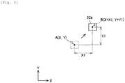
- chip 52a which is one of multiple chips 52 disposed on a support 62 moves will be described with reference to Fig. 5 .
- a flow pressure of a resin acts on chip 52a in a +X-direction and a +Y-direction (upper right in Fig. 5 ) at the time of the molding.
- this case is a case where a molten resin is injected from a position in a -X-direction and a -Y-direction (lower left in Fig. 5 ) with respect to chip 52a on support 62 and the molten resin spreads in the +X-direction and the +Y-direction (upper right in Fig. 5 ).
- chip 52a disposed at first position A of chip 52a moves from first position A to position B in the +X-direction and the +Y-direction in the molding step.
- chip 52a is positioned at position B (X+X1, Y+Y1) which has moved by X1 in the X-direction and +Y1 in the Y-direction from first position A (X, Y).
- the movement amount of chips 52 differs depending on a disposition position of chip 52 on support 62, an injection position of the resin injected to support 62, or the like. That is, the movement amounts for multiple chips 52 disposed on support 62 are different from each other.
- support 62 is peeled from mold body 60 by support peeling section 16(S16). As a result, the chip composite including chip 52 and molding material 54 is formed. By peeling support 62 from mold body 60, the surface of mold body 60 which abuts on support 62 is exposed. That is, in the chip composite, the surface of chip 52 on which electrode pads 53 are formed is exposed.
- position measurement section 18 measures the position of chip 52 in the chip composite (S18). By peeling support 62 in Step S16, in the chip composite, chip 52 is exposed. Position measurement section 18 measures the position of chip 52 by photographing the surface where chip 52 is exposed with a camera. Position measurement section 18 transmits the captured image to control section 30.
- position adjustment section 32 of control section 30 calculates the positional deviation amount of chip 52 based on the image captured by position measurement section 18 (S20).
- Position adjustment section 32 calculates the positional deviation amount of chip 52 based on the first position of each chip 52 and the position of chip 52 which is measured (photographed) in Step S18. For example, in the example illustrated in Fig. 5 , chip 52a is positioned at the position B (X+X1, Y+Y1) moved from the first position A (X, Y).
- position adjustment section 32 calculates the positional deviation amount of chip 52a as the +X1 in the X-direction and the +Y1 in the Y-direction in the molding step (that is, due to the flow pressure of the resin at the time of the molding). Similarly, for each of multiple chips 52, the positional deviation amount from the first position of each chip 52 is calculated based on the position of each chip 52 measurement (photographed) in Step S18 and the first position of chip 52. Thus, by executing the positional deviation amount calculation processing illustrated in Fig. 4 , it is possible to accurately calculate the positional deviation amount caused by the flow pressure of the resin at the time of the molding for each chip 52.
- the above-described positional deviation amount calculation processing can be executed multiple times. By calculating an average value of the positional deviation amounts calculated multiple times, it is possible to more accurately calculate the positional deviation amount of each chip.
- the positional deviation amount of each chip 52 is calculated by the measurement in the present embodiment, configuration is not limited to this.
- the positional deviation amount of each chip 52 may be calculated by simulation based on the disposition position of chip 52, the position at which the resin is injected into the mold, the adhesive force of adhesive tape 66, the flow pressure of the resin, or the like.
- the positions of all chips 52 disposed on support 62 after the molding are measured, but configuration is not limited to this.
- the positions after the molding may be measured only for some selected chips 52 of multiple chips 52, and positions after the molding of the other chips 52 may be predicted based on the measurement results of selected chips 52. For example, when it can be assumed that the positional deviation amount is linearly changed due to the flow pressure, for multiple chips 52 disposed on the same line along a flow direction, the positions after the molding may be measured only for some selected chips 52, and the positions after the molding for the other chips 52 may be calculated by interpolation or extrapolation based on the measurement results of selected chips 52.
- the disposition position of chip 52 is adjusted based on the positional deviation amount of chip 52 after the molding step calculated by the above-described positional deviation amount calculation processing, and package 50 is manufactured.
- chip 52 is disposed on support 62 by chip disposition section 12 (S32).
- chip disposition section 12 disposes the chip 52 at a position (hereinafter, this position may also be referred to as a "second position") set based on the positional deviation amount of chip 52 calculated in the above-described Step S20.
- the second position is set by the position adjustment section 32.
- Position adjustment section 32 sets the second position so that chip 52 after moving by the flow pressure of the resin at the time of the molding (Step S34 illustrated below) is positioned at the first position.
- position adjustment section 32 calculates in Step S20 that chip 52a has moved by +X1 in the X-direction and by +Y1 in the Y-direction. That is, it can be said that chip 52a is moved by +X1 in the X-direction and by +Y1 in the Y-direction due to the flow pressure at the time of the molding. Based on this, position adjustment section 32 sets the second position of chip 52a so that chip 52a is positioned at first position A after the molding step. Specifically, as illustrated in Fig.
- the position adjustment section 32 sets a position C (X-X1, Y-Y1) which is away by -X1 in the X-direction and by -Y1 in the Y-direction from a position at located at first position A, that is, from first position A (X, Y) as the second position.
- the position adjustment section 32 for each of multiple chips 52 disposed on support 62, sets the second position based on the positional deviation amount calculated in Step S20.
- Position adjustment section 32 transmits the set information on the second position of each chip 52 to chip disposition section 12.
- Chip disposition section 12 disposes chips 52 at the second positions according to the received information.
- each of multiple chips 52 is disposed at the second position set in consideration of the positional deviation amount at the time of the molding.
- chip 52a is disposed at second position C which is away by -X1 in the X-direction and -Y1 in the Y-direction from first position A. As described above, chip 52a moves by +X1 in the X-direction and +Y1 in the Y-direction in the molding step.
- each of multiple chips 52 is disposed at the second position of chip 52. Therefore, in the molding step, similarly to chip 52a illustrated in Fig. 7 , each of multiple chips 52 moves from the second position to the first position.
- the molding step similarly to chip 52a illustrated in Fig. 7 , each of multiple chips 52 moves from the second position to the first position.
- Step S34 each chip 52 in mold body 60 after the molding is positioned at the first position of chip 52. Therefore, even in the chip composite, each chip 52 is positioned at the position corresponding to the first position of mold body 60.
- wiring layer forming section 20 forms wiring layer 56 on the surface where chip 52 of the chip composite is exposed (S38).
- each chip 52 is located at the position corresponding to the first position of mold body 60. Therefore, when wiring layer 56 is formed by wiring layer forming section 20, wiring layer 56 can be formed at an accurate position with respect to each chip 52.
- die-cutting section 22 die-cutting (fragmentation) is performed to obtain the structure constituted by chip 52, molding material 54, and wiring layer 56 so as to include individual chips 52 (S40). Accordingly, multiple packages 50 can be manufactured at once. Since each chip 52 is disposed at a desired position in each manufactured package 50, individual packages 50 can be accurately manufactured.
- the position of chip 52 to be disposed on support 62 is set. Accordingly, chip 52 can be positioned at a desired position (first position) after the molding step. Therefore, wiring layer 56 can be formed at an accurate position with respect to chip 52, and package 50 can be manufactured with a high yield.
- the processing of calculating the positional deviation amount of chip 52 may be performed not only before the manufacturing (manufacturing step illustrated in Fig. 6 ) of package 50 but also after the manufacturing of package 50. For example, after the step of peeling support 62 in Step S36 illustrated in Fig. 6 , processing of measuring the position of chip 52 similar to Step S18 may be performed. In a case where the measured position of chip 52 is deviated from the first position, chip 52 may be disposed at a position where the second position is further adjusted based on the measurement result when chip 52 is disposed on support 62. Accordingly, chip 52 can be disposed at a position closer to the first position after the molding step.
- chip 52 when chip 52 is disposed on support 62, chip 52 is disposed so that the surface of chip 52 on which electrode pads 53 are formed abuts on support 62, but configuration is not limited to this.
- chip 52 may be disposed on support 62 so that the surface of chip 52 on which electrode pads 53 are not formed abuts on support 62. That is, in a state in which chip 52 is disposed above support 62, chip 52 may be disposed on support 62 so that the surface of chip 52 on which electrode pads 53 are formed becomes an upper surface.
- molding material 54 is ground until the surface where electrode pads 53 of chip 52 are formed is exposed, and thereafter, wiring layer 56 is formed on the surface of chip 52 where electrode pads 53 are exposed.
- chip 52 after the molding step can be positioned at a desired position (first position).
Landscapes
- Encapsulation Of And Coatings For Semiconductor Or Solid State Devices (AREA)
- Physics & Mathematics (AREA)
- Geometry (AREA)
Abstract
Description
- A technique disclosed in the present specification relates to a technique of manufacturing a package including a chip. In particular, the present specification relates to a technique of manufacturing a package and a mold body which is an intermediate product of the package.
- When a package including a chip is manufactured, the chip may be sealed in the package by covering a periphery of a chip with a molding material. For example,
JP-A-9-148479 JP-A-9-148479 JP-A-9-148479 - When a chip deviates from a predetermined disposition position with respect to a wiring component at the time of manufacturing, the chip and the wiring component cannot be properly connected to each other, and thus, these are discarded, and a problem that a yield is reduced occurs. Therefore, in the package of
JP-A-9-148479 - In a method of manufacturing a mold body disclosed in the present specification, the mold body including a support, a chip disposed at a first position preset on the support, and a molding material covering a periphery of the chip is manufactured. The method of manufacturing a mold body includes a disposition step of disposing the chip at a second position set on the support and a molding step of molding the periphery of the chip disposed on the support in the disposition step with the molding material. In the molding step, the chip disposed at the second position is moved to the first position by a flow pressure of the molding material.
- In the method of manufacturing a mold body, the chip disposed at the second position in the disposition step is moved to the first position preset on the support in the molding step. That is, in the molding step, the chip disposed on the support is moved from the second position to the first position by a flow pressure of the molding material. In the disposition step, by disposing the chip at the second position considering a movement amount at the time of the molding step, the chip is moved to the first position during the molding step. Accordingly, the chip after the molding step can be disposed at a predetermined position (that is, a first position). By manufacturing a package from this mold body, a package can be manufactured with a high yield.
- Moreover, a method of manufacturing a package disclosed in the present specification includes a peeling step of peeling the support from the mold body and a wiring layer forming step of forming a wiring layer connected to the chip after the peeling step.
- In the method of manufacturing a package, a package is manufactured using the mold body manufactured using the manufacturing method. Therefore, it is possible to provide the same operation and effect as in the method of manufacturing a mold body.
- Moreover, a device for manufacturing a mold body disclosed in the present specification manufactures a mold body including a support, a chip disposed at a first position preset on the support, and a molding material covering a periphery of the chip. The device for manufacturing a mold body includes a chip disposition section configured to dispose the chip on the support, a molding section configured to mold the periphery of the chip disposed on the support with the molding material, a position measurement section configured to measure a position of the chip on the support after molding is performed by the molding section, and a position adjustment section configured to adjust a disposition position at which the chip is disposed by the chip disposition section so that the position of the chip after the molding is performed by the molding section becomes the first position, based on a positional deviation amount between a position of the chip before the molding is performed by the molding section and the position of the chip after the molding is performed by the molding section.
- In the mold body manufacturing device, the position of the chip after the molding is performed is measured by the position measurement section. Accordingly it is possible to calculate the positional deviation amount of the chip due to the flow pressure of the molding material during the molding. Further, based on the calculated positional deviation amount, the position adjustment section can adjust the disposition position of the chip so that the chip after the molding is performed disposed at the first position. Therefore, it is possible to manufacture the mold body in which the chip is accurately disposed at the first position. Therefore, it is possible to provide the same operation and effect as in the method of manufacturing a mold body.
-
-
Fig. 1 is a cross-sectional view schematically illustrating a configuration of a package according to an embodiment. -
Fig. 2 is a cross-sectional view illustrating a schematic configuration of a manufacturing step of the package according to the embodiment. -
Fig. 3 is a diagram illustrating a schematic configuration of a package manufacturing device. -
Fig. 4 is a flowchart illustrating an example of processing of calculating a positional deviation amount of the chip. -
Fig. 5 is a diagram for explaining that a chip is moved by a flow pressure of a resin. -
Fig. 6 is a flowchart illustrating an example of a manufacturing step of the package. -
Fig. 7 is a diagram for explaining that the chip disposed at a second position is located at a first position after a molding step. - Main features of an embodiment described below are listed. Technical elements described below are independent technical elements, exhibit technical usefulness alone or by various combinations, and are not limited to combinations described in Claims when filing.
- A method of manufacturing a mold body disclosed in the present specification may include a pre-disposition step of disposing a chip at a first position on a support before a disposition step, a pre-molding step of molding a periphery of the chip disposed at the first position in the pre-disposition step with a molding material, and a measurement step of measuring a position of the chip on the support after the pre-molding step. The second position may be set based on a positional deviation amount between the position of the chip measured in the measurement step and the first position. With such a configuration, it is possible to accurately calculate the positional deviation amount of the chip due to a flow pressure of the molding material from a difference between the position of the chip measured in the measurement step and the first position. Therefore, by setting the second position based on the calculated positional deviation amount, it is possible to accurately dispose the chip at the first position after the molding step.
- In the method of manufacturing a mold body disclosed in the present specification, the mold body may include the support, multiple chips which are disposed on the support, and the molding material which covers peripheries of the multiple chips. The first position and the second position may be individually set for each of the multiple chips. With such a configuration, in a package including the multiple chips, disposition positions of the chips, that is, the first position and the second position, are individually set. In the package including the multiple chips, the flow pressure of the molding material at the time of the molding step applied to each chip differs depending on the position of the chip on the support, a position at which the molding material is injected, or the like. Therefore, by individually setting the first position and the second position for each chip, it is possible to accurately dispose each of the multiple chips at the first position after the molding step. As a result, all the chips can be disposed at predetermined positions after the molding step, and a package can be manufactured with a high yield.
- Hereinafter, a method of
manufacturing package 50 according to an embodiment will be described. First,package 50 manufactured in the present embodiment andmold body 60 which is an intermediate product thereof will be described. -
Fig. 1 schematically illustrates a configuration ofpackage 50. As illustrated inFig. 1 ,package 50 includeschip 52,molding material 54, andwiring layer 56. In the present embodiment,package 50 is a Fan-Out Wafer Level Package (FOWLP) or a Fan-Out Panel Level Package (FOPLP). -
Chip 52 has a flat plate shape and includesmultiple electrode pads 53 on one surface. Inchip 52, the surface on whichelectrode pads 53 are formed abuts onwiring layer 56, and other surfaces are covered withmolding material 54.Wiring layer 56 includes a wire or a bump (not illustrated) (hereinafter, simply referred to as a "wire") which is formed to electrically connect to each ofelectrode pads 53. Whenpackage 50 is mounted on a circuit board or the like,wiring layer 56 is disposed so as to abut on the circuit board or the like. - Next,
mold body 60 which is the intermediate product ofpackage 50 will be described. Here, in order to explainmold body 60, an outline of a manufacturing step ofpackage 50 will also be described. -
Fig. 2 schematically illustrates the manufacturing step ofpackage 50. As illustrated inFig. 2(a) , first,multiple chips 52 are placed onsupport 62.Support 62 is composed ofglass plate 64 andadhesive tape 66 which is adhered to a surface ofglass plate 64 Inadhesive tape 66, an adhesive is applied on both surfaces thereof, one surface is adhered to a surface ofglass plate 64, and chips 52 are adhered to the other surface. When chips 52 are placed on support 62 (that is, adhesive tape 66), chips 52 are fixed at positions placed byadhesive tape 66.Multiple chips 52 are respectively fixed at predetermined positions on onesupport 62. - Next, as illustrated in
Fig. 2(b) , a periphery of eachchip 52 is covered withmolding material 54. In the present embodiment, the intermediate product in this state, that is, in a state in whichmultiple chips 52 are disposed onsupport 62 and the peripheries ofmultiple chips 52 are covered withmolding material 54 is referred to as "mold body 60". In other words,mold body 60 includes onesupport 62,multiple chips 52 which abut onsupport 62, andmolding material 54 which covers each ofmultiple chips 52. - Next, as illustrated in
Fig. 2(c) ,support 62 is peeled frommold body 60. Then, chip 52 (specifically, the surface on whichelectrode pad 53 ofchip 52 is formed) is exposed. Next, as illustrated inFig. 2 (d) ,wiring layer 56 is formed on the surface to which eachchip 52 is exposed. Then, as illustrated inFig. 2 (e) , die-cutting (fragmentation) is performed to obtain a structure constituted bychip 52,molding material 54, andwiring layer 56 so as to includeindividual chips 52. In this manner,multiple packages 50 are manufactured at once. - Next,
package manufacturing device 10 formanufacturing package 50 will be described. As illustrated inFig. 3 ,package manufacturing device 10 includes achip disposition section 12, amolding section 14, asupport peeling section 16, aposition measurement section 18, a wiringlayer forming section 20, a die-cuttingsection 22, and acontrol section 30. Each ofsections sections sections -
Chip disposition section 12 is configured to disposechip 52 onsupport 62. More specifically,chip disposition section 12 disposesmultiple chips 52 at the set positions onsupport 62. The position ofchip 52 disposed bychip disposition section 12 is controlled bycontrol section 30. That is,chip disposition section 12 disposeschip 52 onsupport 62, based on the information on the disposition position ofchip 52 transmitted fromcontrol section 30.Chip disposition section 12 can use a chip disposition section used in a known package manufacturing device, and thus, a detailed description of a configuration thereof is omitted. As described above,adhesive tape 66 is adhered to surface ofsupport 62 Therefore, whenchip 52 is disposed onsupport 62 bychip disposition section 12,chip 52 is fixed to support 62 by adhesive tape 66 (refer toFig. 2(a) ). -
Molding section 14 is configured to cover the periphery of each ofmultiple chips 52 disposed onsupport 62 withmolding material 54.Molding section 14 can be configured to include a mold which covers one surface ofsupport 62, an injection device which injectsmolding material 54 into the mold, or the like.Molding section 14 can use a molding section used in a known package manufacturing device, and thus, a detailed description of a configuration thereof is omitted. A specific procedure for covering the periphery of each ofmultiple chips 52 disposed onsupport 62 withmolding material 54 will be described below. - First,
support 62 in whichchip 52 is disposed onsupport 62 inchip disposition section 12 is carried inmolding section 14. Next,molding section 14molds molding material 54 on carried-insupport 62. As a resin used formolding material 54, for example, a thermoplastic resin is used, but a type of the resin is not particularly limited and can be appropriately selected according to a type ofpackage 50. Specifically, first,molding section 14 disposes a mold having a recessed section onsupport 62. Specifically,molding section 14 installs the mold so as to covermultiple chips 52 by the recessed section. Next,molding section 14 moldsmultiple chips 52 by injectingmolten molding material 54 into the mold. In this case, pressure from the molten resin injected into the mold acts onchip 52 disposed onsupport 62. As described above,chip 52 is fixed onsupport 62 byadhesive tape 66. However, when a flow pressure of the resin injected into the mold is larger than an adhesive force ofadhesive tape 66,chip 52 moves from the position disposed inchip disposition section 12 in accordance with the flow pressure when the resin spreads into a cavity of the mold.Mold body 60 includingsupport 62,chip 52, andmolding material 54 is formed bychip disposition section 12 and molding section 14 (refer toFig. 2(b) ). -
Support peeling section 16 is configured to peelsupport 62 frommold body 60. Specifically,support peeling section 16 reduces the adhesive force ofadhesive tape 66 adhering to chip 52,molding material 54, andsupport 62 to peelsupport 62 frommold body 60.Support peeling section 16 can a support peeling section used in a known package manufacturing device can be used, and thus, a detailed description of a configuration thereof is omitted. Further, a method of reducing the adhesive force ofadhesive tape 66 is not particularly limited. Hereinafter, a composite ofmultiple chips 52 andmolding material 54 in a state in which support 62 is peeled frommold body 60 may be referred to as a "chip composite". Chip 52 (more specifically, surface on whichelectrode pads 53 of eachchip 52 are formed) is exposed to one surface of the chip composite (refer toFig. 2(c) ). -
Position measurement section 18 is configured to measure the position ofchip 52 in the chip composite. Specifically,position measurement section 18 includes a camera (not illustrated), and measures the position ofchip 52 as follows using the camera. First,position measurement section 18 inverts the chip composite up and down so that the surface of the chip composite in whichchip 52 is exposed faces upward. Next,position measurement section 18 photographs the surface of the chip composite in whichchip 52 is exposed from above to below using a camera. The camera may be installed so as to photograph from below to above so that the chip composite is photographed from below without inverting the chip composite up and down. The captured image is transmitted toControl section 30.Control section 30 calculates the position of eachchip 52 in the image by analyzing the captured image. - Wiring
layer forming section 20 is configured to formwiring layer 56 in the chip composite. Specifically, wiringlayer forming section 20forms wiring layer 56 on the surface of the chip composite in whichchip 52 is exposed (refer toFig. 2 (d) ). Wiringlayer forming section 20forms wiring layer 56 so thatwiring layer 56 is electrically connected to eachelectrode pad 53 ofchip 52 whenchip 52 is disposed at a predetermined position in the chip composite. That is, the wire formed by wiringlayer forming section 20 is designed on an assumption thatchip 52 is disposed at a predetermined position in the chip composite. Therefore, in a case where the position ofchip 52 in the chip composite is deviated, even ifwiring layer 56 is formed,chip 52 andwiring layer 56 may not be electrically connected to each other. - Die-cutting
section 22 is configured to divide a structure in whichwiring layer 56 is formed in the chip composite by wiringlayer forming section 20 intoindividual packages 50. Specifically, die-cuttingsection 22 performs division (fragmentation) so thatindividual chips 52 are included in individual packages 50 (refer toFig. 2(e) ). Wiringlayer forming section 20 and die-cuttingsection 22 can use a wiring layer forming section and a die-cutting section used in a known package manufacturing device, and thus, detailed descriptions of configurations thereof are omitted. - For example,
control section 30 can be constituted by a computer including CPU, ROM, a RAM, or the like. When the computer executes the program,control section 30 functions asposition adjustment section 32 or the like illustrated inFig. 3 . Processing executed bycontrol section 30 will be described in detail later. Further,control section 30 is connected to chipdisposition section 12,molding section 14,support peeling section 16,position measurement section 18, wiringlayer forming section 20, and die-cuttingsection 22, and controlsrespective sections - Next, a method of
manufacturing package 50 will be described in detail. As described above, in a process ofmanufacturing package 50,mold body 60 which is the intermediate product is manufactured.Mold body 60 is manufactured by disposingchip 52 onsupport 62 and then performing molding so as to cover the periphery ofchip 52 withmolding material 54. However, the position ofchip 52 inmold body 60 may be deviated by the flow pressure ofmolding material 54 at the time of the molding. If the position ofchip 52 inmold body 60 is deviated, when wiringlayer 56 is formed in the subsequent manufacturing step, the position of the wire inwiring layer 56 is deviated with respect tochip 52, and thus,chip 52 and the wire is not electrically connected to each other. In the present embodiment,chip 52 after the molding step so as to be positioned at a desired position (hereinafter, this position may also be referred to as a "first position") to adjust the position ofchip 52 when disposingchip 52 onsupport 62. - Before
package 50 is manufactured, in order to calculate a positional deviation amount ofchip 52 due to the molding step, positional deviation amount calculation processing is performed. Hereinafter, the positional deviation amount calculation processing will be described in detail. - As illustrated in
Fig. 4 , first,chip disposition section 12 disposeschip 52 at the first position (the position on the design) on support 62 (S12).Multiple chips 52 are disposed onsupport 62. Accordingly,chip disposition section 12 disposesmultiple chips 52 onsupport 62 at the first positions thereof. - Next, molding is performed by molding section 14 (S14). That is,
mold body 60 includingsupport 62,chip 52, andmolding material 54 is formed. Specifically, support 62 (specifically,support 62 on whichmultiple chips 52 are placed) is carried fromchip disposition section 12 tomolding section 14.Molding section 14 disposes the mold onsupport 62 so as to covermultiple chips 52.Molding section 14 covers the peripheries ofmultiple chips 52 disposed onsupport 62 withmolding material 54 by injectingmolten molding material 54 into the mold. In this case, an external force acts onchip 52 by the flow pressure from the molten mold resin onsupport 62. When the flow pressure by the mold resin is larger than the adhesive force ofadhesive tape 66,chip 52 moves from the position where the chip is disposed bychip disposition section 12. Which ofmultiple chips 52 moves, and a movement amount ofchip 52 whenchip 52 moves is caused by a disposition position of eachchip 52, a position at which the molten resin is injected into the mold, or the like. - For example, an example in which
chip 52a which is one ofmultiple chips 52 disposed on asupport 62 moves will be described with reference toFig. 5 . As illustrated inFig. 5 , it is assumed that a flow pressure of a resin acts onchip 52a in a +X-direction and a +Y-direction (upper right inFig. 5 ) at the time of the molding. For example, this case is a case where a molten resin is injected from a position in a -X-direction and a -Y-direction (lower left inFig. 5 ) with respect tochip 52a onsupport 62 and the molten resin spreads in the +X-direction and the +Y-direction (upper right inFig. 5 ). In this case,chip 52a disposed at first position A ofchip 52a moves from first position A to position B in the +X-direction and the +Y-direction in the molding step. For example, after the molding step,chip 52a is positioned at position B (X+X1, Y+Y1) which has moved by X1 in the X-direction and +Y1 in the Y-direction from first position A (X, Y). In this case, the movement amount ofchips 52 differs depending on a disposition position ofchip 52 onsupport 62, an injection position of the resin injected to support 62, or the like. That is, the movement amounts formultiple chips 52 disposed onsupport 62 are different from each other. - Next,
support 62 is peeled frommold body 60 by support peeling section 16(S16). As a result, the chipcomposite including chip 52 andmolding material 54 is formed. By peelingsupport 62 frommold body 60, the surface ofmold body 60 which abuts onsupport 62 is exposed. That is, in the chip composite, the surface ofchip 52 on whichelectrode pads 53 are formed is exposed. - Next,
position measurement section 18 measures the position ofchip 52 in the chip composite (S18). By peelingsupport 62 in Step S16, in the chip composite,chip 52 is exposed.Position measurement section 18 measures the position ofchip 52 by photographing the surface wherechip 52 is exposed with a camera.Position measurement section 18 transmits the captured image to controlsection 30. - Finally,
position adjustment section 32 ofcontrol section 30 calculates the positional deviation amount ofchip 52 based on the image captured by position measurement section 18 (S20).Position adjustment section 32 calculates the positional deviation amount ofchip 52 based on the first position of eachchip 52 and the position ofchip 52 which is measured (photographed) in Step S18. For example, in the example illustrated inFig. 5 ,chip 52a is positioned at the position B (X+X1, Y+Y1) moved from the first position A (X, Y). From two positions A and B,position adjustment section 32 calculates the positional deviation amount ofchip 52a as the +X1 in the X-direction and the +Y1 in the Y-direction in the molding step (that is, due to the flow pressure of the resin at the time of the molding). Similarly, for each ofmultiple chips 52, the positional deviation amount from the first position of eachchip 52 is calculated based on the position of eachchip 52 measurement (photographed) in Step S18 and the first position ofchip 52. Thus, by executing the positional deviation amount calculation processing illustrated inFig. 4 , it is possible to accurately calculate the positional deviation amount caused by the flow pressure of the resin at the time of the molding for eachchip 52. - The above-described positional deviation amount calculation processing can be executed multiple times. By calculating an average value of the positional deviation amounts calculated multiple times, it is possible to more accurately calculate the positional deviation amount of each chip.
- Although the positional deviation amount of each
chip 52 is calculated by the measurement in the present embodiment, configuration is not limited to this. For example, the positional deviation amount of eachchip 52 may be calculated by simulation based on the disposition position ofchip 52, the position at which the resin is injected into the mold, the adhesive force ofadhesive tape 66, the flow pressure of the resin, or the like. - Moreover, in the present embodiment, the positions of all
chips 52 disposed onsupport 62 after the molding are measured, but configuration is not limited to this. The positions after the molding may be measured only for some selectedchips 52 ofmultiple chips 52, and positions after the molding of theother chips 52 may be predicted based on the measurement results of selectedchips 52. For example, when it can be assumed that the positional deviation amount is linearly changed due to the flow pressure, formultiple chips 52 disposed on the same line along a flow direction, the positions after the molding may be measured only for some selectedchips 52, and the positions after the molding for theother chips 52 may be calculated by interpolation or extrapolation based on the measurement results of selectedchips 52. - Next, a step of
manufacturing package 50 will be described. In the manufacturing step ofpackage 50 described below, the disposition position ofchip 52 is adjusted based on the positional deviation amount ofchip 52 after the molding step calculated by the above-described positional deviation amount calculation processing, andpackage 50 is manufactured. - As illustrated in
Fig. 6 , first,chip 52 is disposed onsupport 62 by chip disposition section 12 (S32). In this case,chip disposition section 12 disposes thechip 52 at a position (hereinafter, this position may also be referred to as a "second position") set based on the positional deviation amount ofchip 52 calculated in the above-described Step S20. The second position is set by theposition adjustment section 32.Position adjustment section 32 sets the second position so thatchip 52 after moving by the flow pressure of the resin at the time of the molding (Step S34 illustrated below) is positioned at the first position. - For example, in the example illustrated in
Fig. 5 ,position adjustment section 32 calculates in Step S20 thatchip 52a has moved by +X1 in the X-direction and by +Y1 in the Y-direction. That is, it can be said thatchip 52a is moved by +X1 in the X-direction and by +Y1 in the Y-direction due to the flow pressure at the time of the molding. Based on this,position adjustment section 32 sets the second position ofchip 52a so thatchip 52a is positioned at first position A after the molding step. Specifically, as illustrated inFig. 7 , whenchip 52a moves by +X1 in the X-direction and by +Y1 in the Y-direction, theposition adjustment section 32 sets a position C (X-X1, Y-Y1) which is away by -X1 in the X-direction and by -Y1 in the Y-direction from a position at located at first position A, that is, from first position A (X, Y) as the second position. Similarly, theposition adjustment section 32, for each ofmultiple chips 52 disposed onsupport 62, sets the second position based on the positional deviation amount calculated in Step S20.Position adjustment section 32 transmits the set information on the second position of eachchip 52 to chipdisposition section 12.Chip disposition section 12 disposeschips 52 at the second positions according to the received information. - Then, the molding is performed by molding section 14 (S34). At the time of the molding,
chip 52 is moved by the flow pressure of the resin. In Step S32, each ofmultiple chips 52 is disposed at the second position set in consideration of the positional deviation amount at the time of the molding. For example, in the example illustrated inFig. 7 , in Step S32,chip 52a is disposed at second position C which is away by -X1 in the X-direction and -Y1 in the Y-direction from first position A. As described above,chip 52a moves by +X1 in the X-direction and +Y1 in the Y-direction in the molding step. Therefore, ifchip 52a moves by +X1 in the X-direction and by +Y1 in the Y-direction from the disposed second position C in the molding step and the molding step is completed,chip 52a is positioned at the position moved by +X1 in the X-direction and by +Y1 in the Y-direction from second position C, that is, at first position A. In Step S32, each ofmultiple chips 52 is disposed at the second position ofchip 52. Therefore, in the molding step, similarly tochip 52a illustrated inFig. 7 , each ofmultiple chips 52 moves from the second position to the first position. Thus, by disposingchip 52 at the second position set based on the positional deviation amount calculated in Step S20, it is possible to positionchip 52 at the first position after the molding step. - Next,
support 62 is peeled frommold body 60 by support peeling section 16 (S36). Accordingly, the chip composite is formed. In Step S34, eachchip 52 inmold body 60 after the molding is positioned at the first position ofchip 52. Therefore, even in the chip composite, eachchip 52 is positioned at the position corresponding to the first position ofmold body 60. - Next, wiring
layer forming section 20forms wiring layer 56 on the surface wherechip 52 of the chip composite is exposed (S38). In the chip composite, eachchip 52 is located at the position corresponding to the first position ofmold body 60. Therefore, when wiringlayer 56 is formed by wiringlayer forming section 20,wiring layer 56 can be formed at an accurate position with respect to eachchip 52. - Finally, in die-cutting
section 22, die-cutting (fragmentation) is performed to obtain the structure constituted bychip 52,molding material 54, andwiring layer 56 so as to include individual chips 52 (S40). Accordingly,multiple packages 50 can be manufactured at once. Since eachchip 52 is disposed at a desired position in each manufacturedpackage 50,individual packages 50 can be accurately manufactured. - In the present embodiment, in consideration of the positional deviation amount of
chip 52 which is moved by the flow pressure of the resin at the time of the molding, the position ofchip 52 to be disposed onsupport 62 is set. Accordingly,chip 52 can be positioned at a desired position (first position) after the molding step. Therefore,wiring layer 56 can be formed at an accurate position with respect tochip 52, andpackage 50 can be manufactured with a high yield. - The processing of calculating the positional deviation amount of
chip 52 may be performed not only before the manufacturing (manufacturing step illustrated inFig. 6 ) ofpackage 50 but also after the manufacturing ofpackage 50. For example, after the step of peelingsupport 62 in Step S36 illustrated inFig. 6 , processing of measuring the position ofchip 52 similar to Step S18 may be performed. In a case where the measured position ofchip 52 is deviated from the first position,chip 52 may be disposed at a position where the second position is further adjusted based on the measurement result whenchip 52 is disposed onsupport 62. Accordingly,chip 52 can be disposed at a position closer to the first position after the molding step. - Moreover, in the present embodiment, when
chip 52 is disposed onsupport 62,chip 52 is disposed so that the surface ofchip 52 on whichelectrode pads 53 are formed abuts onsupport 62, but configuration is not limited to this. For example,chip 52 may be disposed onsupport 62 so that the surface ofchip 52 on whichelectrode pads 53 are not formed abuts onsupport 62. That is, in a state in whichchip 52 is disposed abovesupport 62,chip 52 may be disposed onsupport 62 so that the surface ofchip 52 on whichelectrode pads 53 are formed becomes an upper surface. In this case, after the molding step, moldingmaterial 54 is ground until the surface whereelectrode pads 53 ofchip 52 are formed is exposed, and thereafter,wiring layer 56 is formed on the surface ofchip 52 whereelectrode pads 53 are exposed. Even in this configuration, by setting the position ofchip 52 to be disposed onsupport 62 in consideration of the positional deviation amount ofchip 52 which is moved by the flow pressure of the resin at the time of the molding,chip 52 after the molding step can be positioned at a desired position (first position). - The technical elements described in the present specification or the drawings exhibit technical usefulness alone or in various combinations, and are not limited to the combinations described in Claims at the time of filing. In addition, the techniques exemplified in the present specification or the drawings simultaneously achieve multiple purposes, and achieving one of the purposes itself has technical usefulness.
Claims (5)
- A method of manufacturing a mold body including a support, a chip disposed at a first position preset on the support, and a molding material covering a periphery of the chip,
the method comprising:a disposition step of disposing the chip at a second position set on the support; anda molding step of molding the periphery of the chip disposed on the support in the disposition step with the molding material,wherein in the molding step, the chip disposed at the second position is moved to the first position by a flow pressure of the molding material. - The method of manufacturing a mold body according to claim 1, further comprising:a pre-disposition step of disposing the chip at the first position on the support before the disposition step;a pre-molding step of molding the periphery of the chip disposed at the first position in the pre-disposition step with the molding material; anda measurement step of measuring a position of the chip on the support after the pre-molding step,wherein the second position is set based on a positional deviation amount between the position of the chip measured in the measurement step and the first position.
- The method of manufacturing a mold body according to claim 1 or 2,
wherein the mold body includes the support, multiple chips disposed on the support, and the molding material covering peripheries of the multiple chips, and the first position and the second position are individually set for each of the multiple chips. - A method of manufacturing a package comprising:a peeling step of peeling the support from the mold body according to any one of claims 1 to 3; anda wiring layer forming step of forming a wiring layer connected to the chip after the peeling step.
- A device for manufacturing a mold body including a support, a chip disposed at a first position preset on the support, and a molding material covering a periphery of the chip,
the device comprising:a chip disposition section configured to dispose the chip on the support;a molding section configured to mold the periphery of the chip disposed on the support with the molding material;a position measurement section configured to measure a position of the chip on the support after molding is performed by the molding section; anda position adjustment section configured to adjust a disposition position, at which the chip is disposed by the chip disposition section, so that the position of the chip after the molding is performed by the molding section becomes the first position, adjusting the disposition position being performed based on a positional deviation amount between a position of the chip before the molding is performed by the molding section and the position of the chip after the molding is performed by the molding section.
Applications Claiming Priority (1)
| Application Number | Priority Date | Filing Date | Title |
|---|---|---|---|
| PCT/JP2018/026082 WO2020012567A1 (en) | 2018-07-10 | 2018-07-10 | Method of manufacturing mold body and package and device for manufacturing mold body |
Publications (2)
| Publication Number | Publication Date |
|---|---|
| EP3823009A1 true EP3823009A1 (en) | 2021-05-19 |
| EP3823009A4 EP3823009A4 (en) | 2021-07-14 |
Family
ID=69141544
Family Applications (1)
| Application Number | Title | Priority Date | Filing Date |
|---|---|---|---|
| EP18926337.9A Pending EP3823009A4 (en) | 2018-07-10 | 2018-07-10 | MOLD BODY MANUFACTURING PROCESS AS WELL AS CASE AND MOLD BODY MANUFACTURING DEVICE |
Country Status (4)
| Country | Link |
|---|---|
| EP (1) | EP3823009A4 (en) |
| JP (1) | JP7015390B2 (en) |
| KR (1) | KR102454729B1 (en) |
| WO (1) | WO2020012567A1 (en) |
Family Cites Families (6)
| Publication number | Priority date | Publication date | Assignee | Title |
|---|---|---|---|---|
| JPH02241042A (en) * | 1989-03-15 | 1990-09-25 | Seiko Epson Corp | IC sealing method |
| JP3248149B2 (en) | 1995-11-21 | 2002-01-21 | シャープ株式会社 | Resin-sealed semiconductor device and method of manufacturing the same |
| US7674656B2 (en) * | 2006-12-06 | 2010-03-09 | Freescale Semiconductor, Inc. | Die positioning for packaged integrated circuits |
| JP5144634B2 (en) | 2009-12-22 | 2013-02-13 | 日東電工株式会社 | Heat-resistant adhesive sheet for substrate-less semiconductor package manufacturing, and substrate-less semiconductor package manufacturing method using the adhesive sheet |
| JP5584011B2 (en) | 2010-05-10 | 2014-09-03 | 新光電気工業株式会社 | Manufacturing method of semiconductor package |
| JP5734624B2 (en) * | 2010-11-12 | 2015-06-17 | 新光電気工業株式会社 | Manufacturing method of semiconductor package |
-
2018
- 2018-07-10 JP JP2020529887A patent/JP7015390B2/en active Active
- 2018-07-10 EP EP18926337.9A patent/EP3823009A4/en active Pending
- 2018-07-10 KR KR1020207025310A patent/KR102454729B1/en active Active
- 2018-07-10 WO PCT/JP2018/026082 patent/WO2020012567A1/en not_active Ceased
Also Published As
| Publication number | Publication date |
|---|---|
| WO2020012567A1 (en) | 2020-01-16 |
| EP3823009A4 (en) | 2021-07-14 |
| KR102454729B1 (en) | 2022-10-13 |
| JP7015390B2 (en) | 2022-02-02 |
| KR20200116490A (en) | 2020-10-12 |
| JPWO2020012567A1 (en) | 2021-02-15 |
Similar Documents
| Publication | Publication Date | Title |
|---|---|---|
| EP0860871B1 (en) | Method of manufacturing a semiconductor device | |
| CN105643855B (en) | Electronic unit, its manufacturing method and manufacturing device | |
| CN109257888B (en) | A circuit board double-sided packaging method, structure and mobile terminal | |
| JP6541746B2 (en) | Resin molding apparatus and method of manufacturing resin molded article | |
| US9847237B2 (en) | Method and apparatus for manufacturing semiconductor module | |
| JP6400509B2 (en) | Manufacturing method of electronic parts | |
| US9691697B2 (en) | Semiconductor device and method of manufacturing semiconductor device | |
| JP2017170627A (en) | Mold product manufacturing method and mold product | |
| US10141237B2 (en) | Fingerprint recognition module and manufacturing method therefor | |
| CN101901770A (en) | Method for manufacturing integrated circuit package structure | |
| TWI698940B (en) | Semiconductor packaging method, image processing element, camera device and electronic equipment based on molding technology | |
| JP2012114126A (en) | Substrate splitting device and method of manufacturing electronic component | |
| KR20190024869A (en) | Transfer method and mounting method | |
| US20050106786A1 (en) | Method of manufacturing a semiconductor device | |
| JP7015390B2 (en) | Mold body and package manufacturing method, and mold body manufacturing equipment | |
| JP2003124262A (en) | Method for manufacturing semiconductor device | |
| KR20180083789A (en) | Method for manufacturing circuit component and circuit component | |
| KR101783711B1 (en) | Semiconductor package and manufacturing method thereof | |
| KR20140095406A (en) | Resin encapsulating method of flip chip parts | |
| US20080197465A1 (en) | Semiconductor device and method of manufacturing the same | |
| KR101661919B1 (en) | Manufacturing method of semiconductor package | |
| KR101670894B1 (en) | Manufacturing method of semiconductor package | |
| JP6093834B2 (en) | Dummy frame, resin mold evaluation method, mold die evaluation method, and mold die manufacturing method | |
| JPH03284857A (en) | Manufacture of semiconductor device | |
| JP2012114305A (en) | Dummy frame and resin molding method |
Legal Events
| Date | Code | Title | Description |
|---|---|---|---|
| STAA | Information on the status of an ep patent application or granted ep patent |
Free format text: STATUS: THE INTERNATIONAL PUBLICATION HAS BEEN MADE |
|
| PUAI | Public reference made under article 153(3) epc to a published international application that has entered the european phase |
Free format text: ORIGINAL CODE: 0009012 |
|
| STAA | Information on the status of an ep patent application or granted ep patent |
Free format text: STATUS: REQUEST FOR EXAMINATION WAS MADE |
|
| 17P | Request for examination filed |
Effective date: 20201218 |
|
| AK | Designated contracting states |
Kind code of ref document: A1 Designated state(s): AL AT BE BG CH CY CZ DE DK EE ES FI FR GB GR HR HU IE IS IT LI LT LU LV MC MK MT NL NO PL PT RO RS SE SI SK SM TR |
|
| A4 | Supplementary search report drawn up and despatched |
Effective date: 20210616 |
|
| RIC1 | Information provided on ipc code assigned before grant |
Ipc: H01L 21/56 20060101AFI20210610BHEP Ipc: H01L 23/00 20060101ALI20210610BHEP Ipc: H01L 23/538 20060101ALN20210610BHEP |
|
| DAV | Request for validation of the european patent (deleted) | ||
| DAX | Request for extension of the european patent (deleted) | ||
| P01 | Opt-out of the competence of the unified patent court (upc) registered |
Effective date: 20230328 |