EP3822992B1 - Verfahren zum laden eines supraleitenden magnetsystems mit einem hauptsupraleitenden massenmagneten und einem abschirmenden supraleitenden massenmagneten - Google Patents
Verfahren zum laden eines supraleitenden magnetsystems mit einem hauptsupraleitenden massenmagneten und einem abschirmenden supraleitenden massenmagneten Download PDFInfo
- Publication number
- EP3822992B1 EP3822992B1 EP19209166.8A EP19209166A EP3822992B1 EP 3822992 B1 EP3822992 B1 EP 3822992B1 EP 19209166 A EP19209166 A EP 19209166A EP 3822992 B1 EP3822992 B1 EP 3822992B1
- Authority
- EP
- European Patent Office
- Prior art keywords
- shield
- main
- superconductor
- magnet
- bulk
- Prior art date
- Legal status (The legal status is an assumption and is not a legal conclusion. Google has not performed a legal analysis and makes no representation as to the accuracy of the status listed.)
- Active
Links
Images


Classifications
-
- H—ELECTRICITY
- H01—ELECTRIC ELEMENTS
- H01F—MAGNETS; INDUCTANCES; TRANSFORMERS; SELECTION OF MATERIALS FOR THEIR MAGNETIC PROPERTIES
- H01F6/00—Superconducting magnets; Superconducting coils
- H01F6/006—Supplying energising or de-energising current; Flux pumps
- H01F6/008—Electric circuit arrangements for energising superconductive electromagnets
-
- H—ELECTRICITY
- H01—ELECTRIC ELEMENTS
- H01F—MAGNETS; INDUCTANCES; TRANSFORMERS; SELECTION OF MATERIALS FOR THEIR MAGNETIC PROPERTIES
- H01F6/00—Superconducting magnets; Superconducting coils
- H01F6/04—Cooling
-
- G—PHYSICS
- G01—MEASURING; TESTING
- G01R—MEASURING ELECTRIC VARIABLES; MEASURING MAGNETIC VARIABLES
- G01R33/00—Arrangements or instruments for measuring magnetic variables
- G01R33/20—Arrangements or instruments for measuring magnetic variables involving magnetic resonance
- G01R33/28—Details of apparatus provided for in groups G01R33/44 - G01R33/64
- G01R33/38—Systems for generation, homogenisation or stabilisation of the main or gradient magnetic field
- G01R33/381—Systems for generation, homogenisation or stabilisation of the main or gradient magnetic field using electromagnets
- G01R33/3815—Systems for generation, homogenisation or stabilisation of the main or gradient magnetic field using electromagnets with superconducting coils, e.g. power supply therefor
-
- G—PHYSICS
- G01—MEASURING; TESTING
- G01R—MEASURING ELECTRIC VARIABLES; MEASURING MAGNETIC VARIABLES
- G01R33/00—Arrangements or instruments for measuring magnetic variables
- G01R33/20—Arrangements or instruments for measuring magnetic variables involving magnetic resonance
- G01R33/28—Details of apparatus provided for in groups G01R33/44 - G01R33/64
- G01R33/42—Screening
- G01R33/421—Screening of main or gradient magnetic field
-
- H—ELECTRICITY
- H01—ELECTRIC ELEMENTS
- H01F—MAGNETS; INDUCTANCES; TRANSFORMERS; SELECTION OF MATERIALS FOR THEIR MAGNETIC PROPERTIES
- H01F13/00—Apparatus or processes for magnetising or demagnetising
- H01F13/003—Methods and devices for magnetising permanent magnets
-
- H—ELECTRICITY
- H01—ELECTRIC ELEMENTS
- H01F—MAGNETS; INDUCTANCES; TRANSFORMERS; SELECTION OF MATERIALS FOR THEIR MAGNETIC PROPERTIES
- H01F27/00—Details of transformers or inductances, in general
- H01F27/34—Special means for preventing or reducing unwanted electric or magnetic effects, e.g. no-load losses, reactive currents, harmonics, oscillations, leakage fields
- H01F27/36—Electric or magnetic shields or screens
-
- H—ELECTRICITY
- H01—ELECTRIC ELEMENTS
- H01F—MAGNETS; INDUCTANCES; TRANSFORMERS; SELECTION OF MATERIALS FOR THEIR MAGNETIC PROPERTIES
- H01F6/00—Superconducting magnets; Superconducting coils
-
- G—PHYSICS
- G01—MEASURING; TESTING
- G01R—MEASURING ELECTRIC VARIABLES; MEASURING MAGNETIC VARIABLES
- G01R33/00—Arrangements or instruments for measuring magnetic variables
- G01R33/20—Arrangements or instruments for measuring magnetic variables involving magnetic resonance
- G01R33/28—Details of apparatus provided for in groups G01R33/44 - G01R33/64
- G01R33/32—Excitation or detection systems, e.g. using radio frequency signals
- G01R33/34—Constructional details, e.g. resonators, specially adapted to MR
- G01R33/34015—Temperature-controlled RF coils
- G01R33/34023—Superconducting RF coils
-
- H—ELECTRICITY
- H01—ELECTRIC ELEMENTS
- H01F—MAGNETS; INDUCTANCES; TRANSFORMERS; SELECTION OF MATERIALS FOR THEIR MAGNETIC PROPERTIES
- H01F6/00—Superconducting magnets; Superconducting coils
- H01F6/06—Coils, e.g. winding, insulating, terminating or casing arrangements therefor
Definitions
- the invention relates to a method for charging a superconductor magnet system, the superconductor magnet system comprising a main superconductor bulk magnet.
- Superconductors can be used to generate strong magnetic fields (or magnetic flux densities).
- the magnetic field is generated by an electric current running within the superconductor, typically wherein the superconductor forms a coil or ring for this purpose ("superconductor magnet”), and the magnetic field is obtained in a superconductor bore.
- the electric current can run in a closed superconducting electric circuit at a practically constant current strength, without a need for a connection to an electric current source once charged (“persistent mode").
- Coil type superconductor magnet apparatus are typically charged with a directly connected electric current source, and when the charging is complete, a superconducting switch is closed to establish the persistent mode.
- Superconductor bulk magnets which are based on closed ring-shaped superconducting structures, no electric contacts are necessary.
- Superconductor bulk magnets may be charged by a procedure known as "field cooling", e.g. described in US 7,859,374 B2 .
- field cooling e.g. described in US 7,859,374 B2 .
- the superconductor bulk magnet located within a cryostat is placed in an electrical charger magnet. Initially, the temperature of the superconductor bulk magnet is kept above T crit , and the electrical charger magnet is ramped up until a desired magnetic field has been reached. Then the temperature within the cryostat is lowered below T crit , so that the superconductor bulk magnet becomes superconducting. Then the electrical charger magnet is ramped down.
- the superconductor bulk magnet may be removed from the electrical charger magnet.
- the magnetic field within the superconductor bore stays constant and can be used, for example for NMR measurements.
- the cryostat should provide a room temperature bore, which in turn is arranged within the superconductor bore.
- the superconductor bulk magnet not only generates (or conserves) a magnetic field in its superconductor bore, but also generates a magnetic field on its outside (“stray field").
- This outside stray field is in general not desired, since it may disturb electrical equipment nearby, and even may be dangerous to persons carrying for example a pacemaker.
- US 7,859,374 B2 proposes to place a shielding of steel sheets around the cryostat containing a superconductor bulk magnet after the electrical charger has been removed.
- the steel sheets will reduce the stray field in the vicinity of the superconductor bulk magnet.
- the ferromagnetic material necessary for shielding is heavy and takes a lot of space, what is particularly disadvantageous for benchtop size magnet systems.
- Post-published European patent application 19 170 280.2 also describes a superconductor bulk magnet equipped with ferromagnetic shields.
- the bulk tubes may be used to keep external magnetic fields from reaching the inside of the bulk tubes.
- EP 3 492 941 A1 a magnetization method for a bulk magnetic structure is described, wherein after a basic magnetization step, the bulk magnetic structure is further magnetized by controlling at least one of a temperature controller or a magnetic field generator, for obtaining a more uniform magnetic field distribution.
- US 2006/0252650 A1 describes a superconducting permanent magnet comprising a plurality of bulk superconductors arranged in parallel.
- JP H09 74012 A describes a superconducting magnet device with a refrigerant container partitioned into two coaxial refrigerant chambers. Each chamber contains a cylindrical body of a superconducting multi-layer composite. Further, each chamber has an own coolant injector port and connection via a cock to a common refrigerant source.
- the inventive procedure achieves the charging of both the radially inner main superconductor bulk magnet with a main persistent current, and the radially outer shield superconductor bulk magnet with a shield persistent current.
- the main persistent current and the shield persistent current have opposite current directions ("opposite polarity"), so in the surroundings of the superconductor magnet system, their corresponding magnetic fields (or magnetic flux densities) are opposed to each other and therefore cancel out each other, at least partially, and preferably practically completely. Accordingly, the stray field is reduced by an active shielding.
- the main persistent current of the main superconductor bulk magnet results from a take-over of magnetic flux from the charger magnet when the charger current I charger is reduced from the first current I 1 (which is >0) to the second current I 2 (which is ⁇ 0).
- the main superconductor bulk magnet is superconducting, and traps the magnetic flux in its interior.
- the inventive method provides that the conductivity states (normally conducting or superconducting) are chosen temporarily different for the main superconductor bulk magnet and the shield superconductor bulk magnet during the charging procedure.
- their temperatures T main , T shield are set to different values during some of the steps, in particular steps c) and d). Accordingly, the main superconductor bulk magnet and the shield superconductor bulk magnet are, at least temporarily, thermally decoupled during the inventive method.
- a (main or shield) superconductor bulk magnet when a (main or shield) superconductor bulk magnet is below its critical temperature, it will conserve any induced electric currents, and thus trap the magnetic flux in its interior (inside its superconductor bore). Note that the induced (persistent) current stays, in accordance with the invention, below the critical current at the respective operation temperature then, i.e. it does not reach the critical current, so the trapping of the magnetic flux may be accomplished completely.
- the operation temperature should be chosen sufficiently far below the respective critical temperature.
- the inventive method does not require heavy and bulky ferromagnetic shielding plates, but instead may accomplish the shielding with a relatively small shield superconductor bulk magnet.
- the active shielding by means of the shield superconductor bulk magnet in accordance with the invention is much more efficient per weight.
- the shield superconductor bulk magnet is placed in the same vacuum container of the cryostat system as the main superconductor bulk magnet with some distance to it for thermal decoupling; however, it is also possible to have different vacuum containers for the main and shield superconductor bulk magnet.
- both the main superconductor bulk magnet and the shield superconductor bulk magnet contribute to the magnetic field at the sample volume near the magnetic center in the room temperature bore, and therefore both contribute to the homogeneity of the magnetic field there, too.
- the geometry of the shield superconductor bulk magnet is adapted as to improve the homogeneity of the magnetic field that would result from the main superconductor bulk magnet alone. More specifically, the shield superconductor bulk magnet may be used to cancel out leading terms of axial gradients (even orders like Z2 or Z4) in the total magnetic field.
- the shield superconductor bulk magnet typically projects beyond the main superconductor bulk magnet in axial direction, typically by at least 1/10, preferably at least 1/5, of its average radius R shield . Further, typically for the average radius R shield of the shield superconductor bulk magnet and the average radius R main of the main superconductor bulk magnet, R shield ⁇ 1.5* R main applies.
- the main superconductor bulk magnet and the shield superconductor bulk magnet are in general made from a high temperature superconductor material, for example of ReBCO type (Re: rare earth element, in particular Y or Gd) or BSCCO type or of MgB 2 type or of pnictide type (compare WO 2016/161336 A1 ), with T main crit >30 K and T shield crit >30K.
- the main and shield superconductor bulk magnets are substantially of cylindrical shape and have a central (axial) bore. They are generally of closed ring shape, to allow a (main or shield) persistent circular electrical current causing a magnetic field substantially along the axis of the central bore. They may comprise a multitude of axial layers and/or radial layers, and may in particular be made of a multitude of stacked ring elements and/or may comprise a circumferential superconductor coating on a tube type carrier body or bodies.
- T main op ⁇ 0.75*T main crit and T shield op ⁇ 0.75*T shield crit preferably T main op ⁇ 0.60*T main crit and T shield op ⁇ 0.60*T shield crit .
- the normal cryocooler provides cooling power to the main bulk thermal stage and the shield bulk thermal stage only after step f). Then malfunctions of the normal cryocooler, which may be caused by the stray field of the superconductor magnet system during charging (i.e. before the active shielding is in force), can be avoided.
- the normal cryocooler does not need to be operational in strong magnetic fields.
- thermal connection between the normal cryocooler and the main bulk thermal stage and/or the thermal connection between the normal cryocooler and the shield bulk thermal stage include a weak thermal link or a thermal switch, and that the weak thermal link or the thermal switch slows down or blocks heat conduction between the normal cryocooler and the main bulk thermal stage and/or between the normal cryocooler and the shield bulk thermal stage during at least some of step c), step d), step e) and/or step f).
- the thermal switch(es) and weak link(s) avoid a thermal short-circuit of the main bulk thermal stage and the shield thermal stage via the normal cryocooler, and thus facilitate keeping the thermal stages (and thus the main and shield superconductor bulk magnet) temporarily at different temperatures in the course of the inventive method.
- the weak thermal link slows down heat conduction through the weak link to a degree such that said heat conduction is small (e.g. 20 % or less) as compared to a heat conduction (cooling power input) between the auxiliary cryocooler and the thermal stage connected to said weak link.
- the cryostat system includes two normal cryocoolers, with a first of the normal cryocoolers having a thermal connection to a main bulk thermal stage connected to the main superconductor bulk magnet, and a second of the normal cryocoolers having a thermal connection to a shield bulk thermal stage connected to the shield superconductor bulk magnet, and that the first normal cryocooler provides cooling power to the main bulk thermal stage from step c) on and later, and wherein the second normal cryocooler provides cooling power to the shield bulk thermal stage form step e) on and later.
- This design is relatively simple.
- a shield thermal switch may be integrated in the thermal connection of the second normal cryocooler connected to the shield bulk thermal stage.
- the inventive charging method may be performed on an unclaimed superconductor magnet system comprising
- the cooling system comprises a main bulk thermal stage connected to the main superconductor bulk magnet and a shield bulk thermal stage connected to the shield superconductor bulk magnet,
- the main bulk thermal stage and the shield bulk thermal stage comprise separate electrical heaters.
- the heaters allow a finer control of the temperatures of the thermal stages or the main and shield superconductor bulk magnets, and in particular if the respective cooling powers provided to the two thermal stages cannot be controlled independently, or can only coarsely be controlled, then the heaters may guarantee a temperature of the respective thermal stages above the respective critical temperature as required by the inventive method.
- only the shield bulk thermal stage comprises an electrical heater, but not the main bulk thermal stage.
- the cooling system comprises a normal cryocooler and thermal connections of the normal cryocooler to the main bulk thermal stage and to the shield bulk thermal stage.
- the thermal stages facilitate setting the T main and T shield independently during charging.
- the normal cryocooler may provide cooling power at least in the steady state use from step g) on.
- a shield thermal switch is arranged in the thermal connection of the normal cryocooler to the shield bulk thermal stage. Then achieving different temperatures at the two thermal stages, in particular for step d), is facilitated.
- a single normal cryocooler may provide cooling power both during charging and during steady state use.
- a weak thermal link can be arranged in the thermal connection of the normal cryocooler to the shield bulk thermal stage, e.g. reducing the cooling power input from the normal cryocooler to the shield bulk thermal stage to 20% or less as compared to the cooling power input through the thermal connection from the normal cryocooler to the main bulk thermal stage.
- the cooling system further comprises an auxiliary cryocooler
- the thermal connection between the normal cryocooler and the main bulk thermal stage and/or the thermal connection between the normal cryocooler and the shield bulk thermal stage include a weak thermal link or a thermal switch. This avoids a thermal short-circuit of the thermal stages via the normal cryocooler.
- the cooling system includes two normal cryocoolers, with a first of the normal cryocoolers having a thermal connection to the main bulk thermal stage, and a second of the normal cryocoolers having a thermal connection to the shield bulk thermal stage.
- This design is relatively simple.
- the thermal connection of the second of the normal cryocoolers to the shield bulk thermal stage may include a thermal switch.
- a superconducting magnet system may be charged according to the inventive charging method described above with an unclaimed charging system, comprising
- the invention is based on a hardware configuration of nested superconductor bulk rings/cylinders, which are charged by procedure which can be referred to as a "bipolar field-cooling".
- the hardware configuration has to provide that two subdivisions of the nested superconductor bulks are kept at substantially different yet stable temperatures over a relatively long period of time, of the order of several hours.
- the first part of the inventive "bipolar field-cooling" cycle corresponds to a conventional field-cooling process.
- An outsert (“charger”) magnet is ramped up to peak field while the nested superconductor bulks all are above their critical temperature (typically with the nested superconductor bulks above 100 K for REBCO).
- the inner bulk or bulks i.e. the main superconductor bulk magnet, also referred to as "direct bulk” here
- the charger magnet is ramped to zero current (“first charging step”).
- the invention suggests to continue the ramp-down in current to negative currents, providing an inverse polarization of the magnetic field of the charger magnet.
- the outer bulk or bulks i.e. the shield superconductor bulk magnet, also referred to as "shield bulk” here
- shield bulk also referred to as “shield bulk” here
- the critical temperature typically with the direct bulk at 40-60 K for REBCO
- the amplitude (or absolute final current strength in the shield bulk and corresponding magnetic field) of the second ("inverse") charging step can be much smaller than the amplitude (or absolute final current strength in the direct bulk and corresponding magnetic field) of the first ("direct") charging step in order to achieve comparable, opposing dipole moments, leading only to a loss in magnetic field that is small (e.g. 20% or less) as compared to the overall value.
- the wall thickness of the shield bulk can accordingly be much smaller than the wall thickness of the direct bulk.
- the direct charging step corresponds to 7.2 T
- the inverse charging step corresponds to 1.2 T
- the net trapped magnetic flux is 6 T.
- This corresponds to a shield bulk diameter that is roughly twice the diameter of the direct bulk.
- the magnetic flux is the magnetic flux density times area, and area scales as diameter squared.
- Fig. 1 shows a charging system 1, comprising a charger magnet 2 and a superconductor magnet system 3, according to a first design that is suitable to be used to carry out the inventive method.
- the charger magnet 2 comprises here a solenoid type magnet coil 4 wound from a low temperature superconductor wire, such as a NbTi wire.
- the charger magnet 2 is arranged in a charger cryostat 5, which is cooled by a cooling device not shown in detail.
- the charger magnet 2 may be loaded with a charger current I charger via electrical contacts and a current supply, also not shown in detail.
- the charger magnet 2 When charged, the charger magnet 2 generates a charger magnetic flux density B charger within a charger bore 6.
- the charger magnetic flux density B charger is basically parallel to a common axis A at the of the charger bore 6.
- the superconductor magnet system 3 comprises a cryostat system 7, a main superconductor bulk magnet 10 and a shield superconductor bulk magnet 11.
- the cryostat system 7 comprises a common vacuum tank 8 encompassing both the main superconductor bulk magnet 10 and the shield superconductor bulk magnet 11.
- the cryostat system 7 or the common vacuum tank 8, respectively, has a room temperature bore 9 (compare wall 9a) arranged about the common axis A.
- a main or shield superconductor bulk magnet 10, 11 is of a closed ring shape, made of a single superconductor ring structure or of a plurality of ring-shaped superconductor sub-structures such as discs or coatings on a substrate (such as a sheet metal or a foil); the ring-shaped sub-structures are arranged coaxially and stacked axially and/or radially, and may be combined into a so-called "composite bulk" by structurally connecting the sub-structures. All these variants constitute superconductor bulk magnets, suitable for carrying out the inventive method.
- Structures or sub-structures for a superconductor bulk magnet may be grown from a melt; sub-structures to be combined into a "composite bulk" are typically made by coating a substrate.
- a superconductor bulk magnet for carrying out the inventive method allows a trapping of a magnetic field in its bore, wherein the superconductor bulk magnet in general does not possess any electric current supplies, but instead is designed for inductive charging only.
- the shield superconductor bulk magnet 11 shown in Fig. 1 is of generally cylinder jacket type shape, with a shield bulk bore 11a. Radially within the shield bulk bore 11a, there is arranged the main superconductor bulk magnet 10, which is also of generally cylinder jacket type shape, with a main bulk bore 10a. Radially within the main bulk bore 10a, there is arranged the room temperature bore 9 of the cryostat system 7.
- the main superconductor bulk magnet 10 comprises a high temperature superconductor material with a critical temperature T main crit
- the shield superconductor bulk magnet comprises a high temperature superconductor material with a critical temperature T shield crit . It should be noted that the superconductor materials of the two bulk magnets 10, 11 are preferably chosen identically, but may be chosen or differently, if desired.
- the charger magnet 2 or its charger bore 6, respectively, further the shield superconductor bulk magnet 11 or its shield bulk bore 11a, respectively, further the main superconductor bulk magnet 10 or its main bulk bore 10a, and further the room temperature bore 9 of the charger system 7 are arranged coaxially with respect to the common axis A.
- the common axis A defines a z-axis of the superconductor magnet system 3.
- the superconductor magnet system 2 In a charged state, the superconductor magnet system 2 generates a basically homogeneous magnetic flux density (often called B 0 ) basically in parallel to the z-axis in a sample volume 12 located about a magnetic center C within the room temperature bore 9.
- the magnetic flux density B 0 can be used e.g. for NMR measurements on a sample in the sample volume 12.
- the magnetic flux density B 0 results, above all, from a main persistent current IP main running circularly around the sample volume 12 (and around the z axis) in the main superconductor bulk magnet 10.
- a shield persistent current IP shield runs circularly around the sample volume 12 (and around the z axis) in the shield superconductor bulk magnet 11, however with an opposite current direction ("inverse polarity"), what reduces the stray field of the superconductor magnet system 3, but also reduces somewhat the total magnetic flux density at the magnetic center C or the sample volume 12, respectively.
- the current strengths are preferably chosen such that
- the superconductor magnet system 3 is equipped with a cooling system 13.
- the cooling system 13 is designed to allow at least the following three states or temperature distributions of the temperature T main of the main superconductor magnet 10 and T shield of the shield superconductor bulk magnet 11:
- the cooling system 13 comprises a main bulk thermal stage 14 attached to the main superconductor bulk magnet 10, and a shield bulk thermal stage 15 attached to the shield superconductor bulk magnet 11.
- Each thermal stage 14, 15 comprises its own temperature sensor 14a, 15a and its own electrical heater 14b, 15b.
- the thermal stages 14, 15 are arranged on opposite axial sides of the sample volume 12 with respect to the common axis A.
- the cooling system 13 comprises a single normal cryocooler 16, which reaches into the cryostat system 7 or its vacuum tank 8, respectively, and in particular has its cold stage 16a inside the cryostat system 7.
- the normal cryocooler 16 or its cold stage 16a, respectively, is connected via a thermal connection 17 (e.g. a metal thermal conductor) to the main bulk thermal stage 14, and is connected via a thermal connection 18 (e.g. a metal thermal conductor) to the shield bulk thermal stage 15.
- the thermal connection 18 to the shield bulk thermal stage 18 here includes a shield thermal switch 18a.
- the normal cryocooler 16 With the shield thermal switch 18a open, the normal cryocooler 16 provides, when operating, its cooling power basically only to the main bulk thermal stage 14, in particular in order to establish state b) mentioned above; further, a thermal short-circuit of the thermal stages 14, 15 via the cold stage 16a is prevented. With the shield thermal switch 18a closed, the normal cryocooler 16 provides, when operating, cooling power to both thermal stages 14, 15, in particular in order to establish state c) mentioned above. State a) mentioned above is typically established with the normal cryocooler 16 non-operating. By means of the electrical heaters 14b, 15b, unwanted (remaining) cooling power input to the thermal stages 14, 15 may be opposed, in order to ensure a desired temperature above the critical temperature of the corresponding bulk magnet 10, 11.
- the normal cryocooler 16 is here used during both the charging procedure of the superconductor magnet system 3 and during steady state use of the superconductor magnet system 3 after charging, and is permanently installed in the superconductor magnet system 3.
- Fig. 2 shows another equally suitable charging system 1 with a superconductor magnet system 3 similar to the charging system 1 shown in Fig. 1 , so only the major differences are explained in detail.
- the cooling system 13 comprises the permanently installed normal cryocooler 16, and further an auxiliary cryocooler 19 which is installed only for the charging procedure, but is removed during later steady state use.
- the thermal connections 17, 18 from the normal cryocooler 16 to the thermal stages 14, 15 here each comprise a thermal switch 17a, 18a, so the normal cryocooler 16 can be thermally decoupled from the thermal stages 14, 15 during the charging procedure, and also a thermal short-circuit between the thermal stages 14, 15 is prevented during charging.
- the normal cryocooler 16 can be non-operating during the charging procedure, what is useful if the normal cryocooler 16 cannot be operated as long as the stray field of the superconductor magnet system 3 is still high.
- the normal cryocooler 16 can be, for example, of pulse tube type.
- the auxiliary cooler 19 provides for cooling power during the charging procedure, and may direct cooling power independently to the thermal stages 14, 15.
- the auxiliary cryocooler 19 here comprises its own auxiliary cryostat 19b, and provides a fluid coolant (e.g. helium) at its cold stage 19a.
- a forward line 20a for cold coolant leads to the main bulk thermal stage 14, and a return line 20b for warmed coolant leads from the main bulk thermal stage 14 back to the cold stage 19a.
- a flow control device (adjustable valve) 20c is installed in one of the lines, here in the forward line 20a.
- a forward line 21a for cold coolant to the shield bulk thermal stage 15, and a return line 21b for warmed coolant from the shield bulk thermal stage 15 back to the cold stage 19a.
- a flow control device (adjustable valve) 21c is installed in one of the lines, here in the forward line 21a.
- the auxiliary cryocooler 19 is operating at a very low flow of coolant, with the flow control devices 20c, 21c almost shut, since only little cooling power is required.
- the auxiliary cryocooler 19 is operating at a medium flow of coolant, typically with the flow control device 20c being wide open, whereas the flow control device 21c is still almost shut.
- the auxiliary cryocooler 19 is initially operating at high flow of coolant, and typically both flow control devices 20c, 21c are wide open.
- both thermal stages 14, 15 have reached their respective desired low temperature (operation temperature) below the critical temperature of the respective bulk magnet 10, 11, cooling power input is shifted to the then turned-on normal cryocooler 16 (with the thermal switches 17a, 18a closed), and the auxiliary cryocooler 19 is turned off. Then the auxiliary cryocooler 19 typically together with parts of the lines 20a, 20b, 21a, 21b outside the cryostat system 7 and together with the auxiliary cryostat 19b are removed.
- Fig. 3 shows another equally suitable charging system 1 with a superconductor magnet system 3 similar to the charging system 1 shown in Fig. 1 , so again only the major differences are explained in detail.
- the cooling system 13 comprises two permanently installed normal cryocoolers 16, 22. Both normal cryocoolers 16, 22 reach with their respective cold stage 16a, 22a into the cryostat system 7 or its vacuum tank 8, respectively.
- First normal cryocooler 16 has a thermal connection 23 from its cold stage 16a to the main bulk thermal stage 14.
- Second cryocooler 22 has a thermal connection 24 from its cold stage 22a to the shield bulk thermal stage 15.
- the two normal cryocoolers 16, 22 can be operated independently.
- both normal cryocoolers 16, 22 are operating at reduced cooling power.
- typically first normal cryocooler 16 is operating at increased cooling power, and second normal cryocooler 22 is still operating at reduced cooling power.
- typically both normal cryocoolers 16, 22 are operating at increased cooling power.
- the thermal connection 24 from the cold stage 22a of second normal cryocooler 22 to the shield bulk thermal stage 15 may be equipped with a shield thermal switch (not shown), which is closed only for establishing state c).
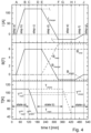
- Fig. 4 illustrates in a schematic diagram the temporal sequence of steps and states during the course of an exemplary variant of the inventive method for charging a superconductor magnet system, for example as illustrated in one of the Figs. 1 , 2 or 3 .
- the time t is plotted, in minutes.
- the applied current I (top third) in Ampere is illustrated, generated magnetic flux densities B in Tesla (middle third) and applied temperatures T in Kelvin (bottom third).
- the method begins in a state a) , wherein the temperature T main of the main superconductor bulk magnet and the temperature T shield of the shield superconductor bulk magnet are above the respective critical temperatures T main crit (here about 95 K) and T shield crit (here about 100 K) at which the bulk magnets become superconducting.
- T main and T shield are both at about 110 K during state a); this may be achieved by applying a low level of cooling power to the thermal stages.
- the superconductor magnet system is arranged in the charger bore of the charger magnet, typically at the premises of the manufacturer of the superconductor magnet system.
- step b) starting at time point A and taking until point of time B, wherein a charger current I charger is applied and increased from zero to a first (positive) current I 1 , here of about 120 A.
- a charger current I charger is applied and increased from zero to a first (positive) current I 1 , here of about 120 A.
- This causes an increase of a magnetic flux density B charger generated by the charger magnet, here to about 6 T.
- all indications of magnet flux relate to the only relevant component in z direction (in parallel to the common axis) and to the magnetic center (and its homogeneous vicinity, i.e. the sample volume) of the superconductor magnet system, for simplicity.
- step b) Since both bulk magnets are in the non-superconducting state, any currents induced therein during step b) decay quickly, so no noticable magnetic flux densities B main from the main superconductor bulk magnet or B shield from the shield superconductor bulk magnet are noted in the diagram. However, after step b), a short relaxation period from time point B to time point C is awaited.
- a step c) between time points C and D, the temperature T main of the main superconductor bulk magnet is lowered to an operation temperature T main op of the main superconductor bulk magnet, with T main op ⁇ T main crit ; note that T main op corresponds to a "maximum" for T main after step c).
- a short relaxation time is awaited between time points D and E.
- the charger current I charger is lowered from the first (positive) current I 1 to a second (negative) current I 2 .
- This causes a corresponding decrease of the magnetic flux density B charger generated by the charger magnet, here from about 6 T to about -1.2 T.
- a circular (positive) current I main (not shown in the diagram) is induced in the main superconductor bulk magnet, which is in a superconducting state.
- This induced current I main comes along with a corresponding (proportional) magnetic flux density B main originating from the main superconductor bulk magnet, which increases from zero to here about 7.2 T.
- the magnetic flux densities B charger and B main result during and at the end of step d) in a total magnetic flux density B total , which is constantly at 6 T, corresponding to the magnetic flux density of B charger at the end of step b) before, which is in accordance to the principle that the (total) magnetic flux density inside of a superconducting magnet, here inside of the main superconductor bulk magnet, stays constant. Since the shield superconductor bulk magnet is still non-superconducting, any current induced there decays quickly and is not relevant. Subsequent to step d), between time points F and G, a short relaxation time is again awaited.
- Step e) between time points G and H, comprises lowering the temperature T shield of the shield superconductor bulk magnet from here about 110 K to an operation temperature T shield op of the shield superconductor bulk magnet of here about 50 K; note that T shield op corresponds to a "maximum" for T shield after step e).
- T main op and T shield op are equal at about 50 K, what can be established and maintained relatively easily in a common vacuum tank of a cryostat system and using a common (normal) cryocooler.
- T main op and T shield op at different temperatures, in particular using two separate (normal) cryocoolers, if desired.
- T main and T shield may fluctuate somewhat in accordance with the invention, provided that T main stays at or below T main op from state b) on (i.e.
- T shield stays at or below T shield op from state c) on (i.e. after step e), respectively), and any induced currents in the bulk magnets can be superconductively carried completely, i.e. without reaching the respective critical current carrying capacity of the bulk magnet.
- step f) between time points I and J the charger current I charger is increased from (negative) second current I 2 to zero. This comes along with a corresponding increase of the magnetic flux density B charger generated by the charger magnet from here -1.2 T to zero. This induces a (negative) current I shield (not shown in the diagram) within the shield superconductor bulk magnet, which comes along with a corresponding (proportional) magnetic flux density B shield caused by the shield superconductor bulk magnet, here of about -1.2 T at the end of step f).
- the magnetic flux inside the shield superconductor bulk magnet formerly generated by the charger magnet is trapped by the shield superconductor bulk magnet inside of it, corresponding to a constant flux inside the superconducting shield superconductor bulk magnet.
- the total magnetic flux density B total during and after step f), i.e. the sum of B main , B shield and B charger remains constant at 6 T, corresponding to a constant magnetic flux inside the superconducting main superconductor bulk magnet.
- step f) At the end of step f) at time point J, the steady state of the superconductor magnet system has been reached.
- step g) taking place after time point J, the superconductor magnet system may now be removed from the charger magnet and transported to a site of application.
- the current I main of the main superconductor bulk magnet stays at a (positive) main persistent current IP main (not shown in detail in the diagram), which is proportional to the final B main value of here about 7.2 T, and the current I shield stays at a (negative) shield persistent current IP shield (also not shown in the diagram), which is proportional to the final B shield value of here about -1.2 T.
- the absolute value of the ratio of the final B main and B shield values is about
- 6, so about
- 6 applies here.
- the inventive charging procedure takes about 8 hours.
- the inventive procedure may in other variants take a shorter time, such as 3 hours or less, or may take a longer time, such as 24 hours or more, depending on the thermal coupling between the main and shield superconductor bulk magnets and the cooling system, which counteracts a warming e.g. caused by hysteresis effects during charging.
Landscapes
- Engineering & Computer Science (AREA)
- Power Engineering (AREA)
- Physics & Mathematics (AREA)
- Electromagnetism (AREA)
- Condensed Matter Physics & Semiconductors (AREA)
- General Physics & Mathematics (AREA)
- Health & Medical Sciences (AREA)
- Epidemiology (AREA)
- Containers, Films, And Cooling For Superconductive Devices (AREA)
Claims (12)
- Verfahren zum Laden eines Supraleitermagnetsystems (3),das Supraleitermagnetsystem (3) umfassend- einen Hauptsupraleitervolumenmagneten (10) von allgemein zylindermantelartiger Form mit einer Hauptvolumenbohrung (10a),- einen Abschirmungssupraleitervolumenmagneten (11) von allgemein zylindermantelartiger Form mit einer Abschirmungsvolumenbohrung (11a),wobei der Hauptsupraleitervolumenmagnet (10) radial innerhalb der Abschirmungsvolumenbohrung (11a) platziert ist, und- ein Kryostatsystem (7), das eine Raumtemperaturbohrung (9) aufweist,wobei das Kryostatsystem (7) den Hauptsupraleitervolumenmagneten (10) und den Abschirmungssupraleitervolumenmagneten (11) enthält,wobei der Abschirmungssupraleitervolumenmagnet (11) den Hauptsupraleitervolumenmagneten (10) radial umgibt,wobei der Hauptsupraleitervolumenmagnet (10) und der Abschirmungssupraleitervolumenmagnet (11) zu der Raumtemperaturbohrung (9) koaxial angeordnet sind,und wobei die Raumtemperaturbohrung (9) radial innerhalb der Hauptvolumenbohrung (10a) angeordnet ist,das Verfahren umfassend die folgenden Schritte:Schritt a) Anordnen des Supraleitermagnetsystems (3) mindestens teilweise innerhalb einer Ladegerätbohrung (6) eines Ladegerätmagneten (2), insbesondere wobei die Ladegerätbohrung (6) zu der Raumtemperaturbohrung (9) des Kryostatsystems (7) koaxial angeordnet ist;Schritt b) mit THaupt > THaupt krit und TAbschirmung > TAbschirmung krit, Anlegen eines elektrischen Stroms ILadegerät an den Ladegerätmagneten (2) und Erhöhen von ILadegerät zu einem ersten Strom I1>0,Schritt c) Absenken von THaupt bis oder unterhalb einer Betriebstemperatur THaupt Betr des Hauptsupraleitervolumenmagneten (10), mit THaupt Betr < THaupt krit, während TAbschirmung >TAbschirmung krit beibehalten wird;Schritt d) Absenken von ILadegerät bis zu einem zweiten Strom I2 < 0, wobei ein Hauptdauerstrom IPHaupt in dem Hauptsupraleitervolumenmagneten (10) induziert wird, der unterhalb eines kritischen Stroms des Hauptsupraleitervolumenmagneten (10) bei THaupt bleibt, mit THaupt ≤ THaupt Betr;Schritt e) Absenken von TAbschirmung bis oder unterhalb einer Betriebstemperatur TAbschirmung Betr des Abschirmungssupraleitervolumenmagneten (11), mit TAbschirmung Betr < TAbschirmung krit;Schritt f) Erhöhen von ILadegerät auf Null, wobei ein Abschirmungsdauerstrom IPAbschirmung in dem Abschirmungssupraleitervolumenmagneten (11) induziert wird, der unterhalb eines kritischen Stroms des Abschirmungssupraleitervolumenmagneten (11) bei TAbschirmung bleibt, mit TAbschirmung ≤ TAbschirmung Betr;Schritt g) Entfernen des Supraleitermagnetsystems (3) aus der Ladegerätbohrung (6) des Ladegerätmagneten (2), und Beibehalten von THaupt bei oder unterhalb THaupt Betr mit THaupt Betr < THaupt krit sowie von TAbschirmung bei oder unterhalb TAbschirmung Betr mit TAbschirmung Betr < TAbschirmung krit;mit THaupt: Temperatur des Hauptsupraleitervolumenmagneten (10);THaupt krit: kritische Temperatur des Hauptsupraleitervolumenmagneten (10);TAbschirmung: Temperatur des Abschirmungssupraleitervolumenmagneten (11); undTAbschirmung krit: kritische Temperatur des Abschirmungssupraleitervolumenmagneten (11),wobei die Temperaturen THaupt, TAbschirmung während der Schritte c) und d) auf unterschiedliche Werte eingestellt werden, und wobei der Hauptsupraleitervolumenmagnet (10) und der Abschirmungssupraleitervolumenmagnet (11) während des Ladeverfahrens, mindestens vorübergehend, thermisch entkoppelt sind.
- Verfahren nach Anspruch 1, wobei

- Verfahren nach Anspruch 2, wobei |I2/I1| ≤ 0,25.
- Verfahren nach Anspruch 1 oder 2, wobei
 mit RHaupt: Durchschnittsradius des Hauptsupraleitervolumenmagneten (10); undRAbschirmung: Durchschnittsradius des Abschirmungssupraleitervolumenmagneten (11).
 - Verfahren nach Anspruch 4, wobei

- Verfahren nach einem der vorstehenden Ansprüche, wobei

- Verfahren nach Anspruch 6, wobei

- Verfahren nach einem der Ansprüche 1 bis 7, wobei- das Kryostatsystem (7) einen Kryokühler (16) und thermische Verbindungen (17, 18) des Kryokühlers (16) mit einer Hauptvolumenwärmestufe (14), die mit dem Hauptsupraleitervolumenmagneten (10) verbunden ist, und mit einer Abschirmungsvolumenwärmestufe (15) umfasst, die mit dem Abschirmungssupraleitervolumenmagneten (11) verbunden ist,- während Schritt c) und Schritt d), ein Abschirmungswärmeschalter (18a) in der thermischen Verbindung (18) mit der Abschirmungsvolumenwärmestufe (15) offen ist, und- während Schritt e) und nach Schritt e), der Abschirmungswärmeschalter (18a) geschlossen gehalten wird.
- Verfahren nach einem der Ansprüche 1 bis 7, wobei- zumindest während der Schritte c) bis f) das Kryostatsystem (7) mit einem Hilfskryokühler (19) ausgestattet ist,- während c) bis f) Kühlleistung des Hilfskryokühlers (19) auf eine Hauptvolumenwärmestufe (14) gerichtet ist, die mit dem Hauptsupraleitervolumenmagneten (10) verbunden ist,- während der Schritte e) und f) Kühlleistung des Hilfskryokühlers (19) auf eine Abschirmungsvolumenwärmestufe (15) gerichtet ist, die mit dem Abschirmungssupraleitervolumenmagneten (11) verbunden ist,- nach Schritt f) der Hilfskryokühler (19) aus dem Kryostatsystem (7) entfernt wird,- das Kryostatsystem (7) einen Kryokühler (16) und thermische Verbindungen (17, 18) des Kryokühlers (16) mit der Hauptvolumenwärmestufe (14) und mit der Abschirmungsvolumenwärmestufe (15) umfasst,- und nach Schritt f), der Kryokühler (16) Kühlleistung an der Hauptvolumenwärmestufe (14) und der Abschirmungsvolumenwärmestufe (15) bereitstellt.
- Verfahren nach Anspruch 9, wobei der Kryokühler (16) nur nach Schritt f) Kühlleistung an der Hauptvolumenwärmestufe (14) und der Abschirmungsvolumenwärmestufe (15) bereitstellt.
- Verfahren nach Anspruch 9 oder 10,wobei die Wärmeverbindung (17) zwischen dem Kryokühler (16) und der Hauptvolumenwärmestufe (14) und/oder der thermischen Verbindung (18) zwischen dem Kryokühler (16) und der Abschirmungsvolumenwärmestufe (15) eine schwache thermische Verlinkung oder einen Wärmeschalter (17a, 18a) beinhaltet,und wobei die schwache thermische Verlinkung oder der Wärmeschalter (17a, 18a) eine Wärmeleitung zwischen dem Kryokühler (16) und der Hauptvolumenwärmestufe (14) und/oder zwischen dem Kryokühler (16) und der Abschirmungsvolumenwärmestufe (15) während zumindest einigen von Schritt c), Schritt d), Schritt e) und/oder Schritt f) verlangsamt oder blockiert.
- Verfahren nach einem der Ansprüche 1 bis 7,wobei das Kryostatsystem (7) zwei Kryokühler (16, 22) beinhaltet, wobei ein erster (16) der Kryokühler (16, 22) eine thermische Verbindung (23) mit einer Hauptvolumenwärmestufe (14) aufweist, die mit dem Hauptsupraleitervolumenmagneten (10) verbunden ist, und ein zweiter (22) der Kryokühler (16, 22) eine thermische Verbindung (24) mit einer Abschirmungsvolumenwärmestufe (15) aufweist, die mit dem Abschirmungssupraleitervolumenmagneten (11) verbunden ist,wobei der erste Kryokühler (16) Kühlleistung an der Hauptvolumenwärmestufe (10) von Schritt c) an und später bereitstellt, und wobei der zweite Kryokühler (22) Kühlleistung an der Abschirmungsvolumenwärmestufe (15) von Schritt e) an und später bereitstellt.
Priority Applications (2)
| Application Number | Priority Date | Filing Date | Title |
|---|---|---|---|
| EP19209166.8A EP3822992B1 (de) | 2019-11-14 | 2019-11-14 | Verfahren zum laden eines supraleitenden magnetsystems mit einem hauptsupraleitenden massenmagneten und einem abschirmenden supraleitenden massenmagneten |
| US17/085,314 US11527343B2 (en) | 2019-11-14 | 2020-10-30 | Method for charging a superconductor magnet system, with a main superconductor bulk magnet and a shield superconductor bulk magnet |
Applications Claiming Priority (1)
| Application Number | Priority Date | Filing Date | Title |
|---|---|---|---|
| EP19209166.8A EP3822992B1 (de) | 2019-11-14 | 2019-11-14 | Verfahren zum laden eines supraleitenden magnetsystems mit einem hauptsupraleitenden massenmagneten und einem abschirmenden supraleitenden massenmagneten |
Publications (2)
| Publication Number | Publication Date |
|---|---|
| EP3822992A1 EP3822992A1 (de) | 2021-05-19 |
| EP3822992B1 true EP3822992B1 (de) | 2023-09-06 |
Family
ID=68581600
Family Applications (1)
| Application Number | Title | Priority Date | Filing Date |
|---|---|---|---|
| EP19209166.8A Active EP3822992B1 (de) | 2019-11-14 | 2019-11-14 | Verfahren zum laden eines supraleitenden magnetsystems mit einem hauptsupraleitenden massenmagneten und einem abschirmenden supraleitenden massenmagneten |
Country Status (2)
| Country | Link |
|---|---|
| US (1) | US11527343B2 (de) |
| EP (1) | EP3822992B1 (de) |
Families Citing this family (4)
| Publication number | Priority date | Publication date | Assignee | Title |
|---|---|---|---|---|
| DE102020104497A1 (de) * | 2020-02-20 | 2021-08-26 | Attocube Systems Ag | System zum Bereitstellen eines Magnetfelds für eine Probe |
| EP3910651B1 (de) | 2020-05-14 | 2022-10-26 | Bruker Switzerland AG | Supraleitendes magnetsystem mit individueller temperatursteuerung von axial gestapelten haupt-submagneten |
| CN114613569B (zh) * | 2022-03-14 | 2022-11-11 | 华中科技大学 | 永磁磁环轴向充磁的方法及装置 |
| WO2025071418A1 (en) * | 2023-09-28 | 2025-04-03 | Victoria Link Limited | Passive temperature regulation in superconducting circuits |
Family Cites Families (11)
| Publication number | Priority date | Publication date | Assignee | Title |
|---|---|---|---|---|
| JPH0974012A (ja) * | 1994-09-16 | 1997-03-18 | Hitachi Medical Corp | 超電導多層複合体を用いた超電導磁石装置と着磁方法 |
| JP2004349276A (ja) | 2003-04-25 | 2004-12-09 | Japan Science & Technology Agency | 超電導永久磁石装置 |
| JP2005123231A (ja) * | 2003-10-14 | 2005-05-12 | Japan Superconductor Technology Inc | 超電導磁石装置 |
| DE102004053973B3 (de) | 2004-11-09 | 2006-07-20 | Bruker Biospin Ag | NMR-Spektrometer mit Refrigeratorkühlung |
| US7859374B2 (en) | 2005-10-03 | 2010-12-28 | Massachusetts Institute Of Technology | Annular magnet system for magnetic resonance spectroscopy |
| JP4468388B2 (ja) * | 2007-02-05 | 2010-05-26 | 株式会社日立製作所 | 磁場発生器 |
| WO2016161336A1 (en) | 2015-04-01 | 2016-10-06 | The Florida State University Research Foundation, Inc. | Iron-based superconducting permanent magnet and method of manufacture |
| DE102015218019B4 (de) * | 2015-09-18 | 2019-02-28 | Bruker Biospin Gmbh | Kryostat mit Magnetanordnung, die einen LTS-Bereich und einen HTS-Bereich umfasst |
| US20190178961A1 (en) | 2016-07-27 | 2019-06-13 | Nippon Steel & Sumitomo Metal Corporation | Bulk magnet structure, magnet system for nmr using said bulk magnetic structure and magnetization method for bulk magnet structure |
| JP6610790B2 (ja) * | 2016-07-27 | 2019-11-27 | 日本製鉄株式会社 | バルクマグネット構造体及びnmr用バルクマグネットシステム |
| EP3657193B1 (de) | 2018-11-20 | 2021-02-17 | Bruker Switzerland AG | Verfahren zum magnetisieren eines supraleitenden magneten mit erzeugung eines zusätzlichen magnetfeldes in der supraleiterbohrung |
-
2019
- 2019-11-14 EP EP19209166.8A patent/EP3822992B1/de active Active
-
2020
- 2020-10-30 US US17/085,314 patent/US11527343B2/en active Active
Also Published As
| Publication number | Publication date |
|---|---|
| EP3822992A1 (de) | 2021-05-19 |
| US20210151230A1 (en) | 2021-05-20 |
| US11527343B2 (en) | 2022-12-13 |
Similar Documents
| Publication | Publication Date | Title |
|---|---|---|
| US11527343B2 (en) | Method for charging a superconductor magnet system, with a main superconductor bulk magnet and a shield superconductor bulk magnet | |
| US8384504B2 (en) | Superconducting quick switch | |
| US20100001821A1 (en) | Superconducting quick switch | |
| US11551843B2 (en) | Method for magnetizing a superconductor bulk magnet, with generating an auxiliary magnetic field in the superconductor bore | |
| JP6636405B2 (ja) | Lts部分とhts部分を有するマグネット装置を備えるクライオスタット | |
| US9715958B2 (en) | Method for energizing a superconducting magnet arrangement | |
| US11798720B2 (en) | Superconductor magnet system, with individual temperature control of axially stacked bulk sub-magnets | |
| CN111292914B (zh) | 用于给hts匀场装置充电的方法和磁体布置系统 | |
| CN111433868B (zh) | 超导磁体组件 | |
| US11391800B2 (en) | Shim device, magnet assembly, and method for charging a shim device | |
| US10998127B2 (en) | Superconducting magnet apparatus and method for magnetizing a superconductor bulk magnet by field cooling through a ferromagnetic shield | |
| Overweg | MRI main field magnets | |
| EP4177624B1 (de) | Verfahren zur homogenisierung eines magnetfeldprofils eines supraleitenden magnetsystems mit rückkopplung durch ein gemessenes magnetfeldprofil | |
| US12500019B2 (en) | Method for charging a superconductor bulk magnet by field-cooling, with at least one non-homogeneous magnetic field component of the applied charger magnetic field | |
| Weerakonda et al. | Generating Uniform Magnetic Fields Using Pulse Field Magnetisation |
Legal Events
| Date | Code | Title | Description |
|---|---|---|---|
| PUAI | Public reference made under article 153(3) epc to a published international application that has entered the european phase |
Free format text: ORIGINAL CODE: 0009012 |
|
| STAA | Information on the status of an ep patent application or granted ep patent |
Free format text: STATUS: THE APPLICATION HAS BEEN PUBLISHED |
|
| AK | Designated contracting states |
Kind code of ref document: A1 Designated state(s): AL AT BE BG CH CY CZ DE DK EE ES FI FR GB GR HR HU IE IS IT LI LT LU LV MC MK MT NL NO PL PT RO RS SE SI SK SM TR |
|
| STAA | Information on the status of an ep patent application or granted ep patent |
Free format text: STATUS: REQUEST FOR EXAMINATION WAS MADE |
|
| 17P | Request for examination filed |
Effective date: 20210624 |
|
| RBV | Designated contracting states (corrected) |
Designated state(s): AL AT BE BG CH CY CZ DE DK EE ES FI FR GB GR HR HU IE IS IT LI LT LU LV MC MK MT NL NO PL PT RO RS SE SI SK SM TR |
|
| STAA | Information on the status of an ep patent application or granted ep patent |
Free format text: STATUS: EXAMINATION IS IN PROGRESS |
|
| 17Q | First examination report despatched |
Effective date: 20220607 |
|
| RIC1 | Information provided on ipc code assigned before grant |
Ipc: G01R 33/421 20060101ALI20230427BHEP Ipc: H01F 13/00 20060101ALI20230427BHEP Ipc: H01F 6/04 20060101ALI20230427BHEP Ipc: G01R 33/3815 20060101ALI20230427BHEP Ipc: H01F 6/00 20060101AFI20230427BHEP |
|
| GRAP | Despatch of communication of intention to grant a patent |
Free format text: ORIGINAL CODE: EPIDOSNIGR1 |
|
| STAA | Information on the status of an ep patent application or granted ep patent |
Free format text: STATUS: GRANT OF PATENT IS INTENDED |
|
| INTG | Intention to grant announced |
Effective date: 20230612 |
|
| GRAS | Grant fee paid |
Free format text: ORIGINAL CODE: EPIDOSNIGR3 |
|
| GRAA | (expected) grant |
Free format text: ORIGINAL CODE: 0009210 |
|
| STAA | Information on the status of an ep patent application or granted ep patent |
Free format text: STATUS: THE PATENT HAS BEEN GRANTED |
|
| AK | Designated contracting states |
Kind code of ref document: B1 Designated state(s): AL AT BE BG CH CY CZ DE DK EE ES FI FR GB GR HR HU IE IS IT LI LT LU LV MC MK MT NL NO PL PT RO RS SE SI SK SM TR |
|
| REG | Reference to a national code |
Ref country code: GB Ref legal event code: FG4D |
|
| REG | Reference to a national code |
Ref country code: CH Ref legal event code: EP |
|
| REG | Reference to a national code |
Ref country code: IE Ref legal event code: FG4D |
|
| REG | Reference to a national code |
Ref country code: DE Ref legal event code: R096 Ref document number: 602019036656 Country of ref document: DE |
|
| REG | Reference to a national code |
Ref country code: LT Ref legal event code: MG9D |
|
| REG | Reference to a national code |
Ref country code: NL Ref legal event code: MP Effective date: 20230906 |
|
| PG25 | Lapsed in a contracting state [announced via postgrant information from national office to epo] |
Ref country code: GR Free format text: LAPSE BECAUSE OF FAILURE TO SUBMIT A TRANSLATION OF THE DESCRIPTION OR TO PAY THE FEE WITHIN THE PRESCRIBED TIME-LIMIT Effective date: 20231207 |
|
| P01 | Opt-out of the competence of the unified patent court (upc) registered |
Effective date: 20231221 |
|
| PG25 | Lapsed in a contracting state [announced via postgrant information from national office to epo] |
Ref country code: SE Free format text: LAPSE BECAUSE OF FAILURE TO SUBMIT A TRANSLATION OF THE DESCRIPTION OR TO PAY THE FEE WITHIN THE PRESCRIBED TIME-LIMIT Effective date: 20230906 Ref country code: RS Free format text: LAPSE BECAUSE OF FAILURE TO SUBMIT A TRANSLATION OF THE DESCRIPTION OR TO PAY THE FEE WITHIN THE PRESCRIBED TIME-LIMIT Effective date: 20230906 Ref country code: NO Free format text: LAPSE BECAUSE OF FAILURE TO SUBMIT A TRANSLATION OF THE DESCRIPTION OR TO PAY THE FEE WITHIN THE PRESCRIBED TIME-LIMIT Effective date: 20231206 Ref country code: LV Free format text: LAPSE BECAUSE OF FAILURE TO SUBMIT A TRANSLATION OF THE DESCRIPTION OR TO PAY THE FEE WITHIN THE PRESCRIBED TIME-LIMIT Effective date: 20230906 Ref country code: LT Free format text: LAPSE BECAUSE OF FAILURE TO SUBMIT A TRANSLATION OF THE DESCRIPTION OR TO PAY THE FEE WITHIN THE PRESCRIBED TIME-LIMIT Effective date: 20230906 Ref country code: HR Free format text: LAPSE BECAUSE OF FAILURE TO SUBMIT A TRANSLATION OF THE DESCRIPTION OR TO PAY THE FEE WITHIN THE PRESCRIBED TIME-LIMIT Effective date: 20230906 Ref country code: GR Free format text: LAPSE BECAUSE OF FAILURE TO SUBMIT A TRANSLATION OF THE DESCRIPTION OR TO PAY THE FEE WITHIN THE PRESCRIBED TIME-LIMIT Effective date: 20231207 Ref country code: FI Free format text: LAPSE BECAUSE OF FAILURE TO SUBMIT A TRANSLATION OF THE DESCRIPTION OR TO PAY THE FEE WITHIN THE PRESCRIBED TIME-LIMIT Effective date: 20230906 |
|
| REG | Reference to a national code |
Ref country code: AT Ref legal event code: MK05 Ref document number: 1609673 Country of ref document: AT Kind code of ref document: T Effective date: 20230906 |
|
| PG25 | Lapsed in a contracting state [announced via postgrant information from national office to epo] |
Ref country code: NL Free format text: LAPSE BECAUSE OF FAILURE TO SUBMIT A TRANSLATION OF THE DESCRIPTION OR TO PAY THE FEE WITHIN THE PRESCRIBED TIME-LIMIT Effective date: 20230906 |
|
| PG25 | Lapsed in a contracting state [announced via postgrant information from national office to epo] |
Ref country code: IS Free format text: LAPSE BECAUSE OF FAILURE TO SUBMIT A TRANSLATION OF THE DESCRIPTION OR TO PAY THE FEE WITHIN THE PRESCRIBED TIME-LIMIT Effective date: 20240106 |
|
| PG25 | Lapsed in a contracting state [announced via postgrant information from national office to epo] |
Ref country code: AT Free format text: LAPSE BECAUSE OF FAILURE TO SUBMIT A TRANSLATION OF THE DESCRIPTION OR TO PAY THE FEE WITHIN THE PRESCRIBED TIME-LIMIT Effective date: 20230906 |
|
| PG25 | Lapsed in a contracting state [announced via postgrant information from national office to epo] |
Ref country code: ES Free format text: LAPSE BECAUSE OF FAILURE TO SUBMIT A TRANSLATION OF THE DESCRIPTION OR TO PAY THE FEE WITHIN THE PRESCRIBED TIME-LIMIT Effective date: 20230906 |
|
| PG25 | Lapsed in a contracting state [announced via postgrant information from national office to epo] |
Ref country code: SM Free format text: LAPSE BECAUSE OF FAILURE TO SUBMIT A TRANSLATION OF THE DESCRIPTION OR TO PAY THE FEE WITHIN THE PRESCRIBED TIME-LIMIT Effective date: 20230906 Ref country code: RO Free format text: LAPSE BECAUSE OF FAILURE TO SUBMIT A TRANSLATION OF THE DESCRIPTION OR TO PAY THE FEE WITHIN THE PRESCRIBED TIME-LIMIT Effective date: 20230906 Ref country code: IS Free format text: LAPSE BECAUSE OF FAILURE TO SUBMIT A TRANSLATION OF THE DESCRIPTION OR TO PAY THE FEE WITHIN THE PRESCRIBED TIME-LIMIT Effective date: 20240106 Ref country code: ES Free format text: LAPSE BECAUSE OF FAILURE TO SUBMIT A TRANSLATION OF THE DESCRIPTION OR TO PAY THE FEE WITHIN THE PRESCRIBED TIME-LIMIT Effective date: 20230906 Ref country code: EE Free format text: LAPSE BECAUSE OF FAILURE TO SUBMIT A TRANSLATION OF THE DESCRIPTION OR TO PAY THE FEE WITHIN THE PRESCRIBED TIME-LIMIT Effective date: 20230906 Ref country code: CZ Free format text: LAPSE BECAUSE OF FAILURE TO SUBMIT A TRANSLATION OF THE DESCRIPTION OR TO PAY THE FEE WITHIN THE PRESCRIBED TIME-LIMIT Effective date: 20230906 Ref country code: AT Free format text: LAPSE BECAUSE OF FAILURE TO SUBMIT A TRANSLATION OF THE DESCRIPTION OR TO PAY THE FEE WITHIN THE PRESCRIBED TIME-LIMIT Effective date: 20230906 Ref country code: PT Free format text: LAPSE BECAUSE OF FAILURE TO SUBMIT A TRANSLATION OF THE DESCRIPTION OR TO PAY THE FEE WITHIN THE PRESCRIBED TIME-LIMIT Effective date: 20240108 Ref country code: SK Free format text: LAPSE BECAUSE OF FAILURE TO SUBMIT A TRANSLATION OF THE DESCRIPTION OR TO PAY THE FEE WITHIN THE PRESCRIBED TIME-LIMIT Effective date: 20230906 |
|
| PG25 | Lapsed in a contracting state [announced via postgrant information from national office to epo] |
Ref country code: PL Free format text: LAPSE BECAUSE OF FAILURE TO SUBMIT A TRANSLATION OF THE DESCRIPTION OR TO PAY THE FEE WITHIN THE PRESCRIBED TIME-LIMIT Effective date: 20230906 Ref country code: IT Free format text: LAPSE BECAUSE OF FAILURE TO SUBMIT A TRANSLATION OF THE DESCRIPTION OR TO PAY THE FEE WITHIN THE PRESCRIBED TIME-LIMIT Effective date: 20230906 |
|
| REG | Reference to a national code |
Ref country code: DE Ref legal event code: R097 Ref document number: 602019036656 Country of ref document: DE |
|
| PG25 | Lapsed in a contracting state [announced via postgrant information from national office to epo] |
Ref country code: MC Free format text: LAPSE BECAUSE OF FAILURE TO SUBMIT A TRANSLATION OF THE DESCRIPTION OR TO PAY THE FEE WITHIN THE PRESCRIBED TIME-LIMIT Effective date: 20230906 |
|
| PG25 | Lapsed in a contracting state [announced via postgrant information from national office to epo] |
Ref country code: DK Free format text: LAPSE BECAUSE OF FAILURE TO SUBMIT A TRANSLATION OF THE DESCRIPTION OR TO PAY THE FEE WITHIN THE PRESCRIBED TIME-LIMIT Effective date: 20230906 |
|
| PLBE | No opposition filed within time limit |
Free format text: ORIGINAL CODE: 0009261 |
|
| STAA | Information on the status of an ep patent application or granted ep patent |
Free format text: STATUS: NO OPPOSITION FILED WITHIN TIME LIMIT |
|
| PG25 | Lapsed in a contracting state [announced via postgrant information from national office to epo] |
Ref country code: LU Free format text: LAPSE BECAUSE OF NON-PAYMENT OF DUE FEES Effective date: 20231114 |
|
| PG25 | Lapsed in a contracting state [announced via postgrant information from national office to epo] |
Ref country code: MC Free format text: LAPSE BECAUSE OF FAILURE TO SUBMIT A TRANSLATION OF THE DESCRIPTION OR TO PAY THE FEE WITHIN THE PRESCRIBED TIME-LIMIT Effective date: 20230906 Ref country code: LU Free format text: LAPSE BECAUSE OF NON-PAYMENT OF DUE FEES Effective date: 20231114 Ref country code: DK Free format text: LAPSE BECAUSE OF FAILURE TO SUBMIT A TRANSLATION OF THE DESCRIPTION OR TO PAY THE FEE WITHIN THE PRESCRIBED TIME-LIMIT Effective date: 20230906 Ref country code: SI Free format text: LAPSE BECAUSE OF FAILURE TO SUBMIT A TRANSLATION OF THE DESCRIPTION OR TO PAY THE FEE WITHIN THE PRESCRIBED TIME-LIMIT Effective date: 20230906 |
|
| REG | Reference to a national code |
Ref country code: BE Ref legal event code: MM Effective date: 20231130 |
|
| 26N | No opposition filed |
Effective date: 20240607 |
|
| REG | Reference to a national code |
Ref country code: IE Ref legal event code: MM4A |
|
| PG25 | Lapsed in a contracting state [announced via postgrant information from national office to epo] |
Ref country code: IE Free format text: LAPSE BECAUSE OF NON-PAYMENT OF DUE FEES Effective date: 20231114 |
|
| PG25 | Lapsed in a contracting state [announced via postgrant information from national office to epo] |
Ref country code: BE Free format text: LAPSE BECAUSE OF NON-PAYMENT OF DUE FEES Effective date: 20231130 |
|
| PG25 | Lapsed in a contracting state [announced via postgrant information from national office to epo] |
Ref country code: IE Free format text: LAPSE BECAUSE OF NON-PAYMENT OF DUE FEES Effective date: 20231114 Ref country code: BE Free format text: LAPSE BECAUSE OF NON-PAYMENT OF DUE FEES Effective date: 20231130 |
|
| PG25 | Lapsed in a contracting state [announced via postgrant information from national office to epo] |
Ref country code: BG Free format text: LAPSE BECAUSE OF FAILURE TO SUBMIT A TRANSLATION OF THE DESCRIPTION OR TO PAY THE FEE WITHIN THE PRESCRIBED TIME-LIMIT Effective date: 20230906 |
|
| PG25 | Lapsed in a contracting state [announced via postgrant information from national office to epo] |
Ref country code: BG Free format text: LAPSE BECAUSE OF FAILURE TO SUBMIT A TRANSLATION OF THE DESCRIPTION OR TO PAY THE FEE WITHIN THE PRESCRIBED TIME-LIMIT Effective date: 20230906 |
|
| PG25 | Lapsed in a contracting state [announced via postgrant information from national office to epo] |
Ref country code: CY Free format text: LAPSE BECAUSE OF FAILURE TO SUBMIT A TRANSLATION OF THE DESCRIPTION OR TO PAY THE FEE WITHIN THE PRESCRIBED TIME-LIMIT; INVALID AB INITIO Effective date: 20191114 |
|
| PG25 | Lapsed in a contracting state [announced via postgrant information from national office to epo] |
Ref country code: HU Free format text: LAPSE BECAUSE OF FAILURE TO SUBMIT A TRANSLATION OF THE DESCRIPTION OR TO PAY THE FEE WITHIN THE PRESCRIBED TIME-LIMIT; INVALID AB INITIO Effective date: 20191114 |
|
| REG | Reference to a national code |
Ref country code: CH Ref legal event code: U11 Free format text: ST27 STATUS EVENT CODE: U-0-0-U10-U11 (AS PROVIDED BY THE NATIONAL OFFICE) Effective date: 20251201 |
|
| PG25 | Lapsed in a contracting state [announced via postgrant information from national office to epo] |
Ref country code: TR Free format text: LAPSE BECAUSE OF FAILURE TO SUBMIT A TRANSLATION OF THE DESCRIPTION OR TO PAY THE FEE WITHIN THE PRESCRIBED TIME-LIMIT Effective date: 20230906 |
|
| PGFP | Annual fee paid to national office [announced via postgrant information from national office to epo] |
Ref country code: DE Payment date: 20251118 Year of fee payment: 7 |
|
| PGFP | Annual fee paid to national office [announced via postgrant information from national office to epo] |
Ref country code: GB Payment date: 20251120 Year of fee payment: 7 |
|
| PGFP | Annual fee paid to national office [announced via postgrant information from national office to epo] |
Ref country code: FR Payment date: 20251120 Year of fee payment: 7 |
|
| PGFP | Annual fee paid to national office [announced via postgrant information from national office to epo] |
Ref country code: CH Payment date: 20251201 Year of fee payment: 7 |