EP3819985A1 - Microstrip patch antenna with increased bandwidth - Google Patents
Microstrip patch antenna with increased bandwidth Download PDFInfo
- Publication number
- EP3819985A1 EP3819985A1 EP19208147.9A EP19208147A EP3819985A1 EP 3819985 A1 EP3819985 A1 EP 3819985A1 EP 19208147 A EP19208147 A EP 19208147A EP 3819985 A1 EP3819985 A1 EP 3819985A1
- Authority
- EP
- European Patent Office
- Prior art keywords
- patch
- radiating
- parasitic
- patches
- array
- Prior art date
- Legal status (The legal status is an assumption and is not a legal conclusion. Google has not performed a legal analysis and makes no representation as to the accuracy of the status listed.)
- Granted
Links
Images





Classifications
-
- H—ELECTRICITY
- H01—ELECTRIC ELEMENTS
- H01Q—ANTENNAS, i.e. RADIO AERIALS
- H01Q21/00—Antenna arrays or systems
- H01Q21/06—Arrays of individually energised antenna units similarly polarised and spaced apart
- H01Q21/08—Arrays of individually energised antenna units similarly polarised and spaced apart the units being spaced along or adjacent to a rectilinear path
-
- H—ELECTRICITY
- H01—ELECTRIC ELEMENTS
- H01Q—ANTENNAS, i.e. RADIO AERIALS
- H01Q21/00—Antenna arrays or systems
- H01Q21/06—Arrays of individually energised antenna units similarly polarised and spaced apart
- H01Q21/061—Two dimensional planar arrays
- H01Q21/065—Patch antenna array
-
- H—ELECTRICITY
- H01—ELECTRIC ELEMENTS
- H01Q—ANTENNAS, i.e. RADIO AERIALS
- H01Q1/00—Details of, or arrangements associated with, antennas
- H01Q1/36—Structural form of radiating elements, e.g. cone, spiral, umbrella; Particular materials used therewith
- H01Q1/38—Structural form of radiating elements, e.g. cone, spiral, umbrella; Particular materials used therewith formed by a conductive layer on an insulating support
-
- H—ELECTRICITY
- H01—ELECTRIC ELEMENTS
- H01Q—ANTENNAS, i.e. RADIO AERIALS
- H01Q1/00—Details of, or arrangements associated with, antennas
- H01Q1/48—Earthing means; Earth screens; Counterpoises
-
- H—ELECTRICITY
- H01—ELECTRIC ELEMENTS
- H01Q—ANTENNAS, i.e. RADIO AERIALS
- H01Q1/00—Details of, or arrangements associated with, antennas
- H01Q1/50—Structural association of antennas with earthing switches, lead-in devices or lightning protectors
-
- H—ELECTRICITY
- H01—ELECTRIC ELEMENTS
- H01Q—ANTENNAS, i.e. RADIO AERIALS
- H01Q19/00—Combinations of primary active antenna elements and units with secondary devices, e.g. with quasi-optical devices, for giving the antenna a desired directional characteristic
- H01Q19/005—Patch antenna using one or more coplanar parasitic elements
-
- H—ELECTRICITY
- H01—ELECTRIC ELEMENTS
- H01Q—ANTENNAS, i.e. RADIO AERIALS
- H01Q21/00—Antenna arrays or systems
- H01Q21/0006—Particular feeding systems
-
- H—ELECTRICITY
- H01—ELECTRIC ELEMENTS
- H01Q—ANTENNAS, i.e. RADIO AERIALS
- H01Q5/00—Arrangements for simultaneous operation of antennas on two or more different wavebands, e.g. dual-band or multi-band arrangements
- H01Q5/30—Arrangements for providing operation on different wavebands
- H01Q5/378—Combination of fed elements with parasitic elements
- H01Q5/385—Two or more parasitic elements
-
- H—ELECTRICITY
- H01—ELECTRIC ELEMENTS
- H01Q—ANTENNAS, i.e. RADIO AERIALS
- H01Q9/00—Electrically-short antennas having dimensions not more than twice the operating wavelength and consisting of conductive active radiating elements
- H01Q9/04—Resonant antennas
- H01Q9/0407—Substantially flat resonant element parallel to ground plane, e.g. patch antenna
-
- H—ELECTRICITY
- H01—ELECTRIC ELEMENTS
- H01Q—ANTENNAS, i.e. RADIO AERIALS
- H01Q9/00—Electrically-short antennas having dimensions not more than twice the operating wavelength and consisting of conductive active radiating elements
- H01Q9/04—Resonant antennas
- H01Q9/0407—Substantially flat resonant element parallel to ground plane, e.g. patch antenna
- H01Q9/045—Substantially flat resonant element parallel to ground plane, e.g. patch antenna with particular feeding means
-
- H—ELECTRICITY
- H01—ELECTRIC ELEMENTS
- H01Q—ANTENNAS, i.e. RADIO AERIALS
- H01Q21/00—Antenna arrays or systems
- H01Q21/0006—Particular feeding systems
- H01Q21/0075—Stripline fed arrays
Definitions
- the present disclosure relates to microwave antennas, particularly to microstrip patch antenna arrays.
- High frequency radio transmission and microwave transmission is of great importance to high-speed data transmissions having low power consumption.
- PCBs printed circuit boards
- Microstrip patch antennas are becoming increasingly useful as they can be printed directly onto a circuit board and their low profile and small size suits them particularly to applications where parameters such as space and weight is at a premium.
- Existing patch antennas are typically low cost and are easily fabricated.
- the invention provides a microstrip antenna array comprising: a thin substrate; two or more microstrip radiating patches placed on a first side of the substrate, each radiating patch comprising: an input port; a radiating patch width extending in a longitudinal direction; a radiating patch length extending in a transverse direction, wherein the transverse direction is perpendicular to the longitudinal direction, and wherein the longitudinal and transverse directions are in the plane of the radiating patch; a radiating patch transverse axis along the midpoint of the radiating patch width; and a radiating patch longitudinal axis along the midpoint of the radiating patch length, wherein the two or more radiating patches are spaced in the longitudinal direction such that the radiating patch longitudinal axis of each radiating patch is aligned along a common longitudinal axis; and one or more parasitic patches placed on the first side of the substrate, wherein there is at least one fewer parasitic patches than there are radiating patches, each parasitic patch comprising: a parasitic patch width
- An advantage of the first aspect is to increase the bandwidth of the patch antenna array by around 50% or more, depending on the particular materials and construction of the patch used. Also, the use of a thin substrate has an advantage of increased structural flexibility and reduced manufacturing costs.
- a microstrip is a type of transmission line that may be used for the transmission of microwave, terahertz, or high frequency radio waves.
- Microstrip structures may be fabricated on printed circuit board (PCB) or as part of monolithic microwave integrated circuits (MMICs) using conventional methods known to the skilled person. Such methods include, but are not limited to, milling, screen printing, and chemical etching.
- the microstrip patch antenna may be formed on a PCB by one of those techniques.
- a substrate may be considered to be "thin" when the substrate is significantly smaller in thickness in comparison to the wavelength of the frequency of the antenna on the substrate, specifically in relation to the wavelength of the antenna in the dielectric substrate ⁇ d .
- This wavelength is modified from the wavelength of the signal in free space ⁇ 0 by the relative dielectric constant of the substrate material ⁇ r , where ⁇ d ⁇ ⁇ r ⁇ 1 2 .
- the thin substrate may comprise a single layer of substrate material, where the material may have a thickness of around 1.0 mm or less, such as 0.5 mm, 0.2 mm or 0.1 mm.
- Substrate materials such as Duroid, Teflon or FR4 may be suitable for thin film patch antennas.
- Thin substrates may be more flexible than thicker single layer substrates or multilayer substrates.
- the use of a thin substrate for a patch antenna array may allow the array to be formed around rounded objects or fit into spaces that would otherwise be difficult for arrays using thicker substrates to conform to.
- Microstrip structures may be formed on the conducting layer of a PCB, which is the layer of conducting material on top of the PCB substrate.
- the conducting layer may be relatively thin compared to the thickness of the substrate.
- the shape of a microstrip structure may be two-dimensional in the plane of the conducting layer and the structure may be formed by etching or milling the conducting layer of a PCB to remove unwanted conducting material.
- Each microstrip structure in the conducting plane may have a uniform thickness.
- the ground layer is on the opposite side of the substrate to the conducting layer.
- the ground layer may be uniform in thickness and may be formed from the same material as the conducting layer.
- the ground layer may be defectless or may have defects formed in its surface.
- the ground layer may cover all of the substrate on the side on which it is placed.
- a parasitic element or passive radiator is a conductive element which is not electrically connected to any other component. In other words, parasitic components do not have an input line and are not driven directly.
- the microwave patch antenna comprises at least two radiating patches formed on a substrate.
- the structure as a whole, including the two or more radiating patches, may collectively be referred to as an "array".
- the radiating patches may be formed in single row on a substrate.
- Each radiating patch may be oriented in the same direction on the same substrate.
- Each radiating patch may be equally spaced along the common longitudinal axis in the longitudinal direction of the substrate.
- Each radiating patch may be regularly spaced along the common longitudinal axis such that the radiating transverse axis of each adjacent radiating patch is equidistance from one another.
- the distance between two adjacent radiating patches may be about 0.5 ⁇ ⁇ , or may be in the range of 0.25> ⁇ o to 0.75 ⁇ o . Alternatively, the distance between two radiating patches in an array of more than two radiating patches may not be regular.
- Each radiating patch may have equal dimensions, that is, the radiating patch widths and the radiating patch lengths of each radiating patch are the same.
- radiating patches may have radiating patch widths and/or radiating patch lengths that differ between individual radiating patches or subsets of patches.
- a parasitic patch may be conducting material formed into a single contiguous patch in the plane of the radiating patches.
- the term "parasitic patch” may refer to a structure comprising a number of components. That is, a parasitic patch may comprise a strip of conducting material on the substrate and one or more VIAs, wherein a VIA is an electrical connection between the conducting metal on one side of the substrate and the ground plane on the other side of the substrate and may be a through hole where the edges of the hole are coated in a conducting material.
- a parasitic patch may refer to a structure comprising two or more strips of conducting material formed on the substrate in the plane of the radiating patches.
- One or more VIAs may be placed along the parasitic patch longitudinal axis and divide the conducting metal portion of the parasitic patch into two quarter wavelength ⁇ d /4 resonant portions.
- the quarter wavelength ⁇ d /4 portions may be coupled together through the one or more VIAs. This coupling may create an additional resonance frequency f 3 .
- the distance between VIAs and the diameters of the VIAs is tuned to provide necessary coupling between two quarter wavelength ⁇ d /4 resonance portions.
- VIAs may be positioned to form resonant portions of other lengths.
- the parasitic patch may comprise two or more parasitic microstrip lines are placed between the radiating patches. That is, the parasitic patch may comprise two or more microstrip lines formed in the transverse direction. The transverse microstrip lines may be parallel and they may be of equal width. The length of the two or more parasitic microstrip lines may be around a half wavelength of the signal in substrate ⁇ d /2 at the central working frequency f 0 .
- the gaps between parasitic microstrip lines and radiating patches G P may be tuned to provide a certain strength of coupling k between radiating patches.
- the parasitic microstrip lines may be coupled together through the gap G PML . This coupling may create an additional resonance frequency f 3 .
- the gap between parasitic microstrip lines G PML may be tuned to provide necessary coupling between them. This coupling may be such that ripples in the single response are minimized.
- the parasitic patch structure may have a total parasitic patch width and a total parasitic patch length, wherein these dimensions may encompass all components in a parasitic patch in the conducting plane. These total lengths may include additional features of the parasitic patch, such as VIAs, or may cover the extent of a patch that is formed from more than one parasitic microstrip line.
- the parasitic patch may not be in physical contact with any of the radiating patches in the conducting plane.
- At least one of the one or more parasitic patches may be symmetric about the common longitudinal axis.
- At least one of the one or more parasitic patches may be symmetric about its parasitic patch transverse axis.
- At least one of the two or more radiating patches may be symmetric about its radiating patch transverse axis.
- the microstrip array of the first aspect may use a microstrip feed, which is the excitation of the microstrip antenna by a microstrip line on the same conducting layer.
- a microwave patch antenna may alternatively be fed in a number of other non-limiting ways, such as: directly at the end of the patch; using an inset feed; using a quarter-wave impedance matching transmission line; from underneath using a coaxial cable or probe feed; using coupled feeds; or using aperture feeds.
- the particular type of feed may be dependent upon the particular application of the patch antenna, and is not limited to those mentioned here. Any feedline may be connected to the input port of the radiating patches.
- FIG. 1A shows a top view of the array 100 to display an arrangement of radiating patches 102
- Fig. 1B shows a side view of the array 100.
- the prior art patch antenna array 100 comprises a substrate 104 formed from a single layer of substrate material, a layer of conducting material forming a ground layer 106 on the bottom side of the substrate 104, and a plurality of radiating patches 102 on a top side 108 of the substrate 104.
- Each radiating patch 102 has an input port 110, a radiating patch width W RP extending in a longitudinal direction, and a radiating patch length L RP extending in a transverse direction.
- the each of the plurality of radiating patches 102 are spaced along a common longitudinal axis C and are oriented so that the input ports 110 for each of the radiating patches 102 are oriented in the same direction.
- Each radiating patch 102 also comprises a radiating patch transverse axis T along the midpoint of the radiating patch width W RP .
- the radiating patches 102 may be labelled RP1, RP2 ... RPN, for N number of radiating patches 102.
- the distance between the transverse axes T of two adjacent patches 102, starting from the distance between RP1 and RP2 and moving rightwards may then be labelled S RP1 , S RP2 ... S RP(N-1) .
- the mutual coupling between patches 102 is characterized either by the conductance matrix (G-matrix) or by the scattering matrix (S-matrix).
- a parasitic patch is used. Placing a resonance structure (the parasitic patch) between active radiating patches increases coupling between the radiating patches and provides mutual detuning of radiators. Active radiating patches are radiating patches that are being fed with a signal via the input port of the radiating patch.
- the microstrip antenna array 200 comprises a thin substrate 204 and two or more microstrip radiating patches 202 placed on a first side 208 of the substrate 204.
- Each radiating patch 202 comprises an input port 210, a radiating patch width W RP extending in a longitudinal direction, and a radiating patch length L RP extending in a transverse direction, wherein the transverse direction is perpendicular to the longitudinal direction, and wherein the longitudinal and transverse directions are in the plane of the radiating patch 202.
- Each patch 202 also comprises a radiating patch transverse axis T RP along the midpoint of the radiating patch width W RP and a radiating patch longitudinal axis along the midpoint of the radiating patch length.
- the two or more radiating patches 202 are spaced in the longitudinal direction such that the radiating patch longitudinal axis of each radiating patch 202 is aligned along a common longitudinal axis C.
- the microstrip patch array 200 also comprises one or more parasitic patches 212 placed on the first side 208 of the substrate 204, wherein there are at least one fewer parasitic patches 212 than there are radiating patches 202.
- Each parasitic patch 212 comprises a parasitic patch width W PP extending in the longitudinal direction, a parasitic patch length L PP extending in the transverse direction, a parasitic patch transverse axis T PP along the midpoint of the parasitic patch width, and a parasitic patch longitudinal axis along the midpoint of the parasitic patch length.
- the one or more parasitic patches 212 are spaced in the longitudinal direction such that the parasitic patch longitudinal axis of each parasitic patch 212 is aligned along the common longitudinal axis C.
- Each parasitic patch 212 is positioned between two radiating patches 202 and the parasitic patch transverse axis T PP of each parasitic patch is positioned at the midpoint between the radiating patch transverse axes T RP of the two radiating patches 202 either side of each parasitic patch 212.
- the parasitic patch 212 has such dimensions so that to provide necessary coupling k between radiating patches 202.
- the length of parasitic patch L PP is approximately close to a half wavelength in substrate ⁇ d at a central working frequency f 0 .
- the parasitic patch width W PP and gaps between radiating patches G P are tuned to provide the certain strength of coupling k between radiating patches 202.
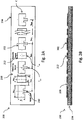
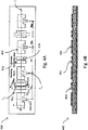
- FIG. 3A and 3B Another example of a microstrip patch antenna array 300 is shown in Figures 3A and 3B .
- the construction of the antenna array 300 is similar to that of the previous example in that the radiating patches 302 are the same and the parasitic patches 312 comprise a strip of conducting metal, each parasitic patch 312 being positioned between two radiating patches 302. That is, the length of parasitic patch L PP approximately is close to half wavelength in substrate ⁇ d /2 at central working frequency f 0 .
- the width of parasitic patch W PP and gaps between radiating patches G P are tuned to provide the certain strength of coupling k between radiating patches.
- the parasitic patches 312 shown in Figure 4 also comprise two VIAs 314 in each patch 312.
- the VIAs 314 are an electrical connection between the conducting metal portion of the parasitic patch 312 and the ground plane, passing though the substrate.
- the VIAs 314 are positioned within the area of the conducting metal portion of the parasitic patch 312 and along the common longitudinal axis C.
- the VIAs 314 are placed along the parasitic patch longitudinal axis and divide the conducting metal portion of the parasitic patch 312 into two quarter wavelength ⁇ d /4 resonant portions 316.
- the quarter wavelength ⁇ d /4 portions 316 are coupled together through the VIAs 314. This coupling creates an additional resonance frequency f 3 .
- the distance between VIAs 314 and their diameters is tuned to provide necessary coupling between the two quarter wavelength ⁇ d /4 resonance portions 316.
- FIG. 4A and 4B Yet another example of a microstrip patch antenna array 400 is shown in Figures 4A and 4B .
- the parasitic patch 412 in this example comprises two parasitic microstrip lines 414 are placed between the radiating patches 402.
- the length of parasitic microstrip lines L PML approximately is close to a half wavelength of the signal in substrate ⁇ d /2 at the central working frequency f 0 .
- Each parasitic microstrip line has a width W PML .
- the gaps between parasitic microstrip lines and radiating patches G P are tuned to provide the certain strength of coupling k between radiating patches 402.
- the parasitic microstrip lines 414 are coupled together through the gap G PML . This coupling creates an additional resonance frequency f 3 .
- the gap between parasitic microstrip lines G PML is tuned to provide necessary coupling between them.
- S-parameters for the prior art antenna array and for each of the examples are shown in Figure 5 .
- S-parameters characterize the mutual coupling between radiating patches, and the S 21 parameter indicates power loss or gain at the output of the system as compared to the energy put into the system.
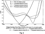
- Figure 6 shows a graph of the voltage standing wave ratio (VSWR) at the input of a radiating patch for each of the prior art and the above example antenna arrays.
- VSWR voltage standing wave ratio
- Figure 7 shows a spherical polar coordinate system, where the x-axis is collinear with the common longitudinal axis, the y-axis is parallel to the transverse direction, and the z-axis is in a direction upwards from the substrate and antenna and is perpendicular to the conducting plane.
- the origin of the coordinate axis is at the midpoint between two radiating patches.
- the mutual coupling between the radiating patches and the parasitic patches causes a slight distortion of the radiating characteristic of radiating patch G( ⁇ ) and reduces the gain of the radiating patch no higher than 1.5 dB, which is appropriate for many applications.
Landscapes
- Waveguide Aerials (AREA)
- Variable-Direction Aerials And Aerial Arrays (AREA)
Abstract
Description
- The present disclosure relates to microwave antennas, particularly to microstrip patch antenna arrays.
- High frequency radio transmission and microwave transmission, particularly in the 1 to 10 GHz range, is of great importance to high-speed data transmissions having low power consumption. Additionally, the increasing density of components on printed circuit boards (PCBs) calls for advances that reduce the size of individual components on the PCB to facilitate further component density increases.
- Microstrip patch antennas are becoming increasingly useful as they can be printed directly onto a circuit board and their low profile and small size suits them particularly to applications where parameters such as space and weight is at a premium. Existing patch antennas are typically low cost and are easily fabricated.
- Viewed from a first aspect, the invention provides a microstrip antenna array comprising: a thin substrate; two or more microstrip radiating patches placed on a first side of the substrate, each radiating patch comprising: an input port; a radiating patch width extending in a longitudinal direction; a radiating patch length extending in a transverse direction, wherein the transverse direction is perpendicular to the longitudinal direction, and wherein the longitudinal and transverse directions are in the plane of the radiating patch; a radiating patch transverse axis along the midpoint of the radiating patch width; and a radiating patch longitudinal axis along the midpoint of the radiating patch length, wherein the two or more radiating patches are spaced in the longitudinal direction such that the radiating patch longitudinal axis of each radiating patch is aligned along a common longitudinal axis; and one or more parasitic patches placed on the first side of the substrate, wherein there is at least one fewer parasitic patches than there are radiating patches, each parasitic patch comprising: a parasitic patch width extending in the longitudinal direction; a parasitic patch length extending in the transverse direction; a parasitic patch transverse axis along the midpoint of the parasitic patch width; and a parasitic patch longitudinal axis along the midpoint of the parasitic patch length, wherein the one or more parasitic patches are spaced in the longitudinal direction such that the parasitic patch longitudinal axis of each parasitic patch is aligned along the common longitudinal axis, wherein each parasitic patch is positioned between two radiating patches, and wherein the parasitic patch transverse axis of each parasitic patch is positioned at the midpoint between the radiating patch transverse axes of the two radiating patches either side of each parasitic patch.
- An advantage of the first aspect is to increase the bandwidth of the patch antenna array by around 50% or more, depending on the particular materials and construction of the patch used. Also, the use of a thin substrate has an advantage of increased structural flexibility and reduced manufacturing costs.
- A microstrip is a type of transmission line that may be used for the transmission of microwave, terahertz, or high frequency radio waves. Microstrip structures may be fabricated on printed circuit board (PCB) or as part of monolithic microwave integrated circuits (MMICs) using conventional methods known to the skilled person. Such methods include, but are not limited to, milling, screen printing, and chemical etching. Thus, the microstrip patch antenna may be formed on a PCB by one of those techniques.
- A substrate may be considered to be "thin" when the substrate is significantly smaller in thickness in comparison to the wavelength of the frequency of the antenna on the substrate, specifically in relation to the wavelength of the antenna in the dielectric substrate λ d . This wavelength is modified from the wavelength of the signal in free space λ 0 by the relative dielectric constant of the substrate material ε r , where

- Microstrip structures may be formed on the conducting layer of a PCB, which is the layer of conducting material on top of the PCB substrate. The conducting layer may be relatively thin compared to the thickness of the substrate. The shape of a microstrip structure may be two-dimensional in the plane of the conducting layer and the structure may be formed by etching or milling the conducting layer of a PCB to remove unwanted conducting material. Each microstrip structure in the conducting plane may have a uniform thickness.
- The ground layer is on the opposite side of the substrate to the conducting layer. The ground layer may be uniform in thickness and may be formed from the same material as the conducting layer. The ground layer may be defectless or may have defects formed in its surface. The ground layer may cover all of the substrate on the side on which it is placed.
- A parasitic element or passive radiator is a conductive element which is not electrically connected to any other component. In other words, parasitic components do not have an input line and are not driven directly.
- The microwave patch antenna comprises at least two radiating patches formed on a substrate. The structure as a whole, including the two or more radiating patches, may collectively be referred to as an "array". The radiating patches may be formed in single row on a substrate. Each radiating patch may be oriented in the same direction on the same substrate. Each radiating patch may be equally spaced along the common longitudinal axis in the longitudinal direction of the substrate. Each radiating patch may be regularly spaced along the common longitudinal axis such that the radiating transverse axis of each adjacent radiating patch is equidistance from one another. The distance between two adjacent radiating patches may be about 0.5λο , or may be in the range of 0.25>λo to 0.75λo . Alternatively, the distance between two radiating patches in an array of more than two radiating patches may not be regular.
- Each radiating patch may have equal dimensions, that is, the radiating patch widths and the radiating patch lengths of each radiating patch are the same. Alternatively, radiating patches may have radiating patch widths and/or radiating patch lengths that differ between individual radiating patches or subsets of patches.
- A parasitic patch may be conducting material formed into a single contiguous patch in the plane of the radiating patches. Alternatively, the term "parasitic patch" may refer to a structure comprising a number of components. That is, a parasitic patch may comprise a strip of conducting material on the substrate and one or more VIAs, wherein a VIA is an electrical connection between the conducting metal on one side of the substrate and the ground plane on the other side of the substrate and may be a through hole where the edges of the hole are coated in a conducting material. Alternatively again, a parasitic patch may refer to a structure comprising two or more strips of conducting material formed on the substrate in the plane of the radiating patches.
- One or more VIAs may be placed along the parasitic patch longitudinal axis and divide the conducting metal portion of the parasitic patch into two quarter wavelength λd /4 resonant portions. The quarter wavelength λd /4 portions may be coupled together through the one or more VIAs. This coupling may create an additional resonance frequency f 3. In the case of two or more VIAs, the distance between VIAs and the diameters of the VIAs is tuned to provide necessary coupling between two quarter wavelength λd /4 resonance portions. VIAs may be positioned to form resonant portions of other lengths.
- As another alternative, the parasitic patch may comprise two or more parasitic microstrip lines are placed between the radiating patches. That is, the parasitic patch may comprise two or more microstrip lines formed in the transverse direction. The transverse microstrip lines may be parallel and they may be of equal width. The length of the two or more parasitic microstrip lines may be around a half wavelength of the signal in substrate λd /2 at the central working frequency f 0. The gaps between parasitic microstrip lines and radiating patches GP may be tuned to provide a certain strength of coupling k between radiating patches. The parasitic microstrip lines may be coupled together through the gap GPML. This coupling may create an additional resonance frequency f 3. The gap between parasitic microstrip lines GPML may be tuned to provide necessary coupling between them. This coupling may be such that ripples in the single response are minimized.
- The parasitic patch structure may have a total parasitic patch width and a total parasitic patch length, wherein these dimensions may encompass all components in a parasitic patch in the conducting plane. These total lengths may include additional features of the parasitic patch, such as VIAs, or may cover the extent of a patch that is formed from more than one parasitic microstrip line. The parasitic patch may not be in physical contact with any of the radiating patches in the conducting plane.
- At least one of the one or more parasitic patches may be symmetric about the common longitudinal axis.
- At least one of the one or more parasitic patches may be symmetric about its parasitic patch transverse axis.
- At least one of the two or more radiating patches may be symmetric about its radiating patch transverse axis.
- The microstrip array of the first aspect may use a microstrip feed, which is the excitation of the microstrip antenna by a microstrip line on the same conducting layer. A microwave patch antenna may alternatively be fed in a number of other non-limiting ways, such as: directly at the end of the patch; using an inset feed; using a quarter-wave impedance matching transmission line; from underneath using a coaxial cable or probe feed; using coupled feeds; or using aperture feeds. The particular type of feed may be dependent upon the particular application of the patch antenna, and is not limited to those mentioned here. Any feedline may be connected to the input port of the radiating patches.
- Certain embodiments of the disclosure will now be described by way of example only and with reference to the accompanying drawings in which:
-
Figure 1A is a top view of a prior art microstrip antenna array. -
Figure 1B is a side view of a prior art microstrip antenna array. -
Figure 2A is a top view of an example microstrip antenna array. -
Figure 2B is a side view of an example microstrip antenna array. -
Figure 3A is a top view of another example microstrip antenna array. -
Figure 3B is a side view of another example microstrip antenna array. -
Figure 4A is a top view of yet another example microstrip antenna array. -
Figure 4B is a side view of yet another example microstrip antenna array. -
Figure 5 shows S-parameters for the prior art antenna array and for each of the example antenna arrays. -
Figure 6 shows a graph of the voltage standing wave ratio (VSWR) at the input of a radiating patch for each of the prior art and example antenna arrays. -
Figure 7 shows a spherical polar coordinate system applied to a microstrip antenna array. -
Figures 8A and 8B are radiation patterns of the prior art patch antenna array and for each of the example arrays at angles of ϕ = 0 and ϕ = 90 based upon the coordinate system shown inFigure 7 . - A prior art
patch antenna array 100 is presented inFigure 1A and 1B , whereFig. 1A shows a top view of thearray 100 to display an arrangement of radiatingpatches 102 andFig. 1B shows a side view of thearray 100. The prior artpatch antenna array 100 comprises asubstrate 104 formed from a single layer of substrate material, a layer of conducting material forming aground layer 106 on the bottom side of thesubstrate 104, and a plurality of radiatingpatches 102 on atop side 108 of thesubstrate 104. Each radiatingpatch 102 has aninput port 110, a radiating patch width WRP extending in a longitudinal direction, and a radiating patch length LRP extending in a transverse direction. The each of the plurality of radiatingpatches 102 are spaced along a common longitudinal axis C and are oriented so that theinput ports 110 for each of the radiatingpatches 102 are oriented in the same direction. - Each radiating
patch 102 also comprises a radiating patch transverse axis T along the midpoint of the radiating patch width WRP. Starting from the leftmost radiating patch inFig. 1A and moving rightwards, the radiatingpatches 102 may be labelled RP1, RP2 ... RPN, for N number of radiatingpatches 102. The distance between the transverse axes T of twoadjacent patches 102, starting from the distance between RP1 and RP2 and moving rightwards may then be labelled SRP1, SRP2 ... SRP(N-1). - The mutual coupling between
patches 102 is characterized either by the conductance matrix (G-matrix) or by the scattering matrix (S-matrix). - The mutual conductance between two rectangular microstrip patches for the radiating patch arrangement is [1]:

- J 0 - the Bessel function of the first kind of order zero;
- Z - the center-to-center separation between the patches and equal to the array step SRP;
- W - the width of the radiating patch;
- L - the length of the radiating patch;
- λ 0 - is the wavelength in free space;
- ε - the permittivity of free space;
- µ - the permeability of free space.
- In the
prior art array 100 shown inFigures 1A and 1B , the fields in the space between the elements are primarily transverse electric (TE) modes and there is not a strong dominant mode surface wave excitation. Therefore, there is reduced coupling between the elements. When the coupling is small, the resonant frequency of the patch radiator is close to the resonant frequency of uncoupled antennas f 0. - When the strength of coupling increases, two resonant frequencies f 1 and f 2 of coupled patches appear. The strength of coupling is described with the coupling coefficient k that can be computed from the following formula:

- f 1 - the lower resonant frequency of coupled antennas;
- f 2 - the upper resonant frequency of coupled antennas.
- To improve the coupling between radiating patches a parasitic patch is used. Placing a resonance structure (the parasitic patch) between active radiating patches increases coupling between the radiating patches and provides mutual detuning of radiators. Active radiating patches are radiating patches that are being fed with a signal via the input port of the radiating patch.
- One example of a microstrip
patch antenna array 200 having parasitic patches is shown inFigures 2A and 2B . Themicrostrip antenna array 200 comprises athin substrate 204 and two or moremicrostrip radiating patches 202 placed on afirst side 208 of thesubstrate 204. Each radiatingpatch 202 comprises aninput port 210, a radiating patch width WRP extending in a longitudinal direction, and a radiating patch length LRP extending in a transverse direction, wherein the transverse direction is perpendicular to the longitudinal direction, and wherein the longitudinal and transverse directions are in the plane of theradiating patch 202. Eachpatch 202 also comprises a radiating patch transverse axis TRP along the midpoint of the radiating patch width WRP and a radiating patch longitudinal axis along the midpoint of the radiating patch length. The two or more radiatingpatches 202 are spaced in the longitudinal direction such that the radiating patch longitudinal axis of each radiatingpatch 202 is aligned along a common longitudinal axis C. - The
microstrip patch array 200 also comprises one or moreparasitic patches 212 placed on thefirst side 208 of thesubstrate 204, wherein there are at least one fewerparasitic patches 212 than there are radiatingpatches 202. Eachparasitic patch 212 comprises a parasitic patch width WPP extending in the longitudinal direction, a parasitic patch length LPP extending in the transverse direction, a parasitic patch transverse axis TPP along the midpoint of the parasitic patch width, and a parasitic patch longitudinal axis along the midpoint of the parasitic patch length. The one or moreparasitic patches 212 are spaced in the longitudinal direction such that the parasitic patch longitudinal axis of eachparasitic patch 212 is aligned along the common longitudinal axis C. - Each
parasitic patch 212 is positioned between two radiatingpatches 202 and the parasitic patch transverse axis TPP of each parasitic patch is positioned at the midpoint between the radiating patch transverse axes TRP of the two radiatingpatches 202 either side of eachparasitic patch 212. - The
parasitic patch 212 has such dimensions so that to provide necessary coupling k between radiatingpatches 202. The length of parasitic patch LPP is approximately close to a half wavelength in substrate λd at a central working frequency f 0. The parasitic patch width WPP and gaps between radiating patches GP are tuned to provide the certain strength of coupling k between radiatingpatches 202. - Another example of a microstrip
patch antenna array 300 is shown inFigures 3A and 3B . The construction of theantenna array 300 is similar to that of the previous example in that the radiatingpatches 302 are the same and theparasitic patches 312 comprise a strip of conducting metal, eachparasitic patch 312 being positioned between two radiatingpatches 302. That is, the length of parasitic patch LPP approximately is close to half wavelength in substrate λd /2 at central working frequency f 0. The width of parasitic patch WPP and gaps between radiating patches GP are tuned to provide the certain strength of coupling k between radiating patches. - The
parasitic patches 312 shown inFigure 4 also comprise twoVIAs 314 in eachpatch 312. TheVIAs 314 are an electrical connection between the conducting metal portion of theparasitic patch 312 and the ground plane, passing though the substrate. TheVIAs 314 are positioned within the area of the conducting metal portion of theparasitic patch 312 and along the common longitudinal axisC. The VIAs 314 are placed along the parasitic patch longitudinal axis and divide the conducting metal portion of theparasitic patch 312 into two quarter wavelength λd /4resonant portions 316. The quarter wavelength λd /4portions 316 are coupled together through theVIAs 314. This coupling creates an additional resonance frequency f 3. The distance between VIAs 314 and their diameters is tuned to provide necessary coupling between the two quarter wavelength λd /4resonance portions 316. - Yet another example of a microstrip
patch antenna array 400 is shown inFigures 4A and 4B . In this example, the radiatingpatches 402 are the same as in the previous two examples. Theparasitic patch 412 in this example comprises twoparasitic microstrip lines 414 are placed between the radiatingpatches 402. The length of parasitic microstrip lines LPML approximately is close to a half wavelength of the signal in substrate λd /2 at the central working frequency f 0. Each parasitic microstrip line has a width WPML. The gaps between parasitic microstrip lines and radiating patches GP are tuned to provide the certain strength of coupling k between radiatingpatches 402. Theparasitic microstrip lines 414 are coupled together through the gap GPML. This coupling creates an additional resonance frequency f 3. The gap between parasitic microstrip lines GPML is tuned to provide necessary coupling between them. - The S-parameters for the prior art antenna array and for each of the examples are shown in
Figure 5 . S-parameters characterize the mutual coupling between radiating patches, and the S21 parameter indicates power loss or gain at the output of the system as compared to the energy put into the system. -
Figure 6 shows a graph of the voltage standing wave ratio (VSWR) at the input of a radiating patch for each of the prior art and the above example antenna arrays. At a VSWR of, 10% of the input power is reflected and this is a level at which the antenna may be considered to be impedance matched with the input feedline. At this value, it can be clearly seen from the graph that the bandwidth for each of the example patch arrays is significantly wider than that of the prior art array. -
Figure 7 shows a spherical polar coordinate system, where the x-axis is collinear with the common longitudinal axis, the y-axis is parallel to the transverse direction, and the z-axis is in a direction upwards from the substrate and antenna and is perpendicular to the conducting plane. The origin of the coordinate axis is at the midpoint between two radiating patches.. -
Figures 8A and 8B are radiation patterns of the prior art patch antenna array and for each of the example arrays at angles of ϕ = 0 and ϕ = 90 based upon the coordinate system shown inFigure 7 . The mutual coupling between the radiating patches and the parasitic patches causes a slight distortion of the radiating characteristic of radiating patch G(θ) and reduces the gain of the radiating patch no higher than 1.5 dB, which is appropriate for many applications.
Claims (15)
- A microstrip antenna array (200; 300; 400) comprising:a thin substrate (204);two or more microstrip radiating patches (202; 302; 402) placed on a first side (208) of the substrate (204), each radiating patch (202; 302; 402) comprising:an input port (210);a radiating patch width (WRP) extending in a longitudinal direction;a radiating patch length (LRP) extending in a transverse direction, wherein the transverse direction is perpendicular to the longitudinal direction, and wherein the longitudinal and transverse directions are in the plane of the radiating patch;a radiating patch transverse axis (TRP) along the midpoint of the radiating patch width; anda radiating patch longitudinal axis along the midpoint of the radiating patch length,wherein the two or more radiating patches are spaced in the longitudinal direction such that the radiating patch longitudinal axis of each radiating patch is aligned along a common longitudinal axis (C); andone or more parasitic patches (212; 312; 412) placed on the first side (208) of the substrate (204), wherein there is at least one fewer parasitic patches than there are radiating patches, each parasitic patch comprising:a parasitic patch width (WPP) extending in the longitudinal direction;a parasitic patch length (LPP) extending in the transverse direction;a parasitic patch transverse axis (TPP) along the midpoint of the parasitic patch width; anda parasitic patch longitudinal axis along the midpoint of the parasitic patch length,wherein the one or more parasitic patches (212; 312; 412) are spaced in the longitudinal direction such that the parasitic patch longitudinal axis of each parasitic patch is aligned along the common longitudinal axis (C), wherein each parasitic patch is positioned between two radiating patches (202; 302; 402), and wherein the parasitic patch transverse axis (TPP) of each parasitic patch is positioned at the midpoint between the radiating patch transverse axes (TRP) of the two radiating patches either side of each parasitic patch.
- The array of claim 1, wherein the radiating patch input lines are positioned along the radiating patch transverse axis.
- The array of claims 1 or 2, wherein the substrate has a thickness of 1.0mm or less.
- The array of claims 1, 2 or 3, wherein the radiating patches are regularly spaced along the common longitudinal axis.
- The array of any preceding claims, wherein the radiating patch transverse axes of adjacent radiating patches are separated by about a half wavelength of an input signal, wherein the wavelength of the signal is modified by the substrate.
- The array of any preceding claim, wherein the parasitic patch length about a half wavelength of an input signal, wherein the wavelength of the signal is modified by the substrate.
- The array of any preceding claim, wherein at least one of the one or more parasitic patches is symmetric about the common longitudinal axis.
- The array of any preceding claim, wherein at least one of the one or more parasitic patches is symmetric about its parasitic patch transverse axis.
- The array of any preceding claim, wherein at least one of the two or more radiating patches is symmetric about its radiating patch transverse axis.
- The array of any preceding claim, wherein the parasitic patch width and gaps between radiating patches GP are tuned to provide the certain strength of coupling k between radiating patches.
- The array of any preceding claim, wherein at least one parasitic patch comprises at least one VIA.
- The array of claim 11, wherein the VIA is positioned along the common longitudinal axis.
- The array of claim 11 or 12, wherein the VIAs are positioned to divide the parasitic patch into two quarter wavelength λd /4 resonant portions.
- The array of any preceding claim, wherein one of the parasitic patches comprises two or more parasitic microstrip lines, the lines being spaced apart along the common longitudinal axis and between two radiating patches.
- The array of claim 14, wherein the gap between the two or more parasitic microstrip lines is tuned to provide necessary coupling between them.
Priority Applications (4)
| Application Number | Priority Date | Filing Date | Title |
|---|---|---|---|
| EP19208147.9A EP3819985B1 (en) | 2019-11-08 | 2019-11-08 | Microstrip patch antenna with increased bandwidth |
| US17/089,955 US11495891B2 (en) | 2019-11-08 | 2020-11-05 | Microstrip patch antenna with increased bandwidth |
| CN202011230773.0A CN112787108A (en) | 2019-11-08 | 2020-11-06 | Microstrip patch antenna with increased bandwidth |
| US17/940,376 US11837791B2 (en) | 2019-11-08 | 2022-09-08 | Microstrip patch antenna with increased bandwidth |
Applications Claiming Priority (1)
| Application Number | Priority Date | Filing Date | Title |
|---|---|---|---|
| EP19208147.9A EP3819985B1 (en) | 2019-11-08 | 2019-11-08 | Microstrip patch antenna with increased bandwidth |
Publications (2)
| Publication Number | Publication Date |
|---|---|
| EP3819985A1 true EP3819985A1 (en) | 2021-05-12 |
| EP3819985B1 EP3819985B1 (en) | 2024-04-24 |
Family
ID=68501525
Family Applications (1)
| Application Number | Title | Priority Date | Filing Date |
|---|---|---|---|
| EP19208147.9A Active EP3819985B1 (en) | 2019-11-08 | 2019-11-08 | Microstrip patch antenna with increased bandwidth |
Country Status (3)
| Country | Link |
|---|---|
| US (2) | US11495891B2 (en) |
| EP (1) | EP3819985B1 (en) |
| CN (1) | CN112787108A (en) |
Cited By (2)
| Publication number | Priority date | Publication date | Assignee | Title |
|---|---|---|---|---|
| CN113937475A (en) * | 2021-10-08 | 2022-01-14 | 南京邮电大学 | Microstrip patch antenna with wide impedance bandwidth and harmonic suppression function |
| CN116169487A (en) * | 2022-11-03 | 2023-05-26 | 烟台大学 | A Cooperative Optimization Method of EBG Decoupling Structure Shape and Layout of Array Antenna |
Families Citing this family (11)
| Publication number | Priority date | Publication date | Assignee | Title |
|---|---|---|---|---|
| FR3089696B1 (en) * | 2018-12-11 | 2020-11-13 | Thales Sa | Wideband guided wave mechanical phase shifting device |
| EP3819985B1 (en) | 2019-11-08 | 2024-04-24 | Carrier Corporation | Microstrip patch antenna with increased bandwidth |
| CN115347380B (en) * | 2021-05-13 | 2025-09-12 | 台达电子工业股份有限公司 | Antenna array device |
| CN113488774B (en) * | 2021-06-29 | 2024-04-12 | 中国信息通信研究院 | A microstrip antenna with in-band pattern diversity and a manufacturing method thereof |
| KR102367163B1 (en) * | 2021-07-05 | 2022-02-23 | 동우 화인켐 주식회사 | Antenna structure and image display device including the same |
| US12046823B2 (en) * | 2022-04-04 | 2024-07-23 | Htc Corporation | Communication device for antenna adjustment |
| US12021319B2 (en) * | 2022-04-19 | 2024-06-25 | Meta Platforms Technologies, Llc | Distributed monopole antenna for enhanced cross-body link |
| TW202406221A (en) * | 2022-04-19 | 2024-02-01 | 美商元平台技術有限公司 | Distributed monopole antenna for enhanced cross-body link |
| WO2024151463A1 (en) * | 2023-01-13 | 2024-07-18 | Metawave Corporation | Antenna in package structure and design method |
| CN116565513A (en) * | 2023-02-06 | 2023-08-08 | 中国科学院空天信息创新研究院 | A single-layer broadband patch antenna and its design method |
| EP4435973A1 (en) * | 2023-03-23 | 2024-09-25 | u-blox AG | Patch antenna array and method for manufacturing a patch antenna array |
Citations (1)
| Publication number | Priority date | Publication date | Assignee | Title |
|---|---|---|---|---|
| WO2017150054A1 (en) * | 2016-03-04 | 2017-09-08 | 株式会社村田製作所 | Array antenna |
Family Cites Families (41)
| Publication number | Priority date | Publication date | Assignee | Title |
|---|---|---|---|---|
| US4812855A (en) | 1985-09-30 | 1989-03-14 | The Boeing Company | Dipole antenna with parasitic elements |
| GB8803451D0 (en) * | 1988-02-15 | 1988-03-16 | British Telecomm | Antenna |
| DE69020215T2 (en) | 1989-04-03 | 1996-02-29 | Raytheon Co | Microstrip line antenna with parasitic elements. |
| GB9002636D0 (en) * | 1990-02-06 | 1990-04-04 | British Telecomm | Antenna |
| US5220335A (en) * | 1990-03-30 | 1993-06-15 | The United States Of America As Represented By The Administrator Of The National Aeronautics And Space Administration | Planar microstrip Yagi antenna array |
| FR2691015B1 (en) * | 1992-05-05 | 1994-10-07 | Aerospatiale | Micro-ribbon type antenna antenna with low thickness but high bandwidth. |
| US5627550A (en) | 1995-06-15 | 1997-05-06 | Nokia Mobile Phones Ltd. | Wideband double C-patch antenna including gap-coupled parasitic elements |
| US5680144A (en) | 1996-03-13 | 1997-10-21 | Nokia Mobile Phones Limited | Wideband, stacked double C-patch antenna having gap-coupled parasitic elements |
| US5745079A (en) | 1996-06-28 | 1998-04-28 | Raytheon Company | Wide-band/dual-band stacked-disc radiators on stacked-dielectric posts phased array antenna |
| US5880694A (en) | 1997-06-18 | 1999-03-09 | Hughes Electronics Corporation | Planar low profile, wideband, wide-scan phased array antenna using a stacked-disc radiator |
| CA2225677A1 (en) | 1997-12-22 | 1999-06-22 | Philippe Lafleur | Multiple parasitic coupling to an outer antenna patch element from inner path elements |
| JP3233895B2 (en) | 1998-02-10 | 2001-12-04 | アルプス電気株式会社 | Display device and driving method thereof |
| AU759369B2 (en) | 1998-02-20 | 2003-04-10 | Qualcomm Incorporated | Substrate antenna incorporating an element preventing the coupling of energy between antenna and conductors |
| US6421012B1 (en) | 2000-07-19 | 2002-07-16 | Harris Corporation | Phased array antenna having patch antenna elements with enhanced parasitic antenna element performance at millimeter wavelength radio frequency signals |
| WO2003034545A1 (en) | 2001-10-16 | 2003-04-24 | Fractus, S.A. | Multifrequency microstrip patch antenna with parasitic coupled elements |
| US7068234B2 (en) | 2003-05-12 | 2006-06-27 | Hrl Laboratories, Llc | Meta-element antenna and array |
| KR100542829B1 (en) | 2003-09-09 | 2006-01-20 | 한국전자통신연구원 | High Gain Wideband Microstrip Patch Antenna for Transmit and Receive and Array Arrays |
| US7038624B2 (en) | 2004-06-16 | 2006-05-02 | Delphi Technologies, Inc. | Patch antenna with parasitically enhanced perimeter |
| WO2006035881A1 (en) * | 2004-09-30 | 2006-04-06 | Toto Ltd. | Microstrip antenna and high frequency sensor using microstrip antenna |
| US6999030B1 (en) | 2004-10-27 | 2006-02-14 | Delphi Technologies, Inc. | Linear polarization planar microstrip antenna array with circular patch elements and co-planar annular sector parasitic strips |
| US7221322B1 (en) | 2005-12-14 | 2007-05-22 | Harris Corporation | Dual polarization antenna array with inter-element coupling and associated methods |
| US7420519B2 (en) | 2005-12-16 | 2008-09-02 | Harris Corporation | Single polarization slot antenna array with inter-element coupling and associated methods |
| US7408520B2 (en) | 2005-12-16 | 2008-08-05 | Harris Corporation | Single polarization slot antenna array with inter-element capacitive coupling plate and associated methods |
| JP2009089217A (en) * | 2007-10-02 | 2009-04-23 | Panasonic Corp | Array antenna device |
| US7973734B2 (en) | 2007-10-31 | 2011-07-05 | Lockheed Martin Corporation | Apparatus and method for covering integrated antenna elements utilizing composite materials |
| US7864117B2 (en) * | 2008-05-07 | 2011-01-04 | Nokia Siemens Networks Oy | Wideband or multiband various polarized antenna |
| US20110260925A1 (en) | 2010-04-23 | 2011-10-27 | Laurian Petru Chirila | Multiband internal patch antenna for mobile terminals |
| US8466844B2 (en) | 2010-06-16 | 2013-06-18 | Sony Ericsson Mobile Communications Ab | Multi-band antennas using multiple parasitic coupling elements and wireless devices using the same |
| US20130169503A1 (en) * | 2011-12-30 | 2013-07-04 | Mohammad Fakharzadeh Jahromi | Parasitic patch antenna |
| IL218625A (en) | 2012-03-14 | 2017-10-31 | Israel Aerospace Ind Ltd | Phased array antenna |
| US9755311B2 (en) | 2012-05-29 | 2017-09-05 | Samsung Electronics Co., Ltd. | Circularly polarized patch antennas, antenna arrays, and devices including such antennas and arrays |
| US9941584B2 (en) * | 2013-01-09 | 2018-04-10 | Hrl Laboratories, Llc | Reducing antenna array feed modules through controlled mutual coupling of a pixelated EM surface |
| CN103199337A (en) * | 2013-03-21 | 2013-07-10 | 西安电子科技大学 | Circularly polarized microstrip antenna |
| IL231026B (en) | 2014-02-18 | 2018-07-31 | Mti Wireless Edge Ltd | Wideband dual-polarized patch antenna array and methods useful in conjunction therewith |
| EP3010086B1 (en) | 2014-10-13 | 2017-11-29 | Fraunhofer-Gesellschaft zur Förderung der angewandten Forschung e.V. | Phased array antenna |
| CN105720364B (en) | 2016-04-06 | 2019-03-05 | 华南理工大学 | A dual-polarized filter antenna with high selectivity and low cross-polarization |
| US20180123245A1 (en) | 2016-10-28 | 2018-05-03 | Broadcom Corporation | Broadband antenna array for wireless communications |
| WO2018111690A1 (en) * | 2016-12-12 | 2018-06-21 | Skyworks Solutions, Inc. | Frequency and polarization reconfigurable antenna systems |
| KR101942343B1 (en) * | 2017-08-30 | 2019-01-25 | 한국과학기술원 | Series-Fed E-shaped Patch Antenna Array with Co-polarized Parasitic Patches |
| CN207690998U (en) * | 2018-01-19 | 2018-08-03 | 中国人民解放军陆军工程大学 | A Microstrip Patch Antenna with Broadband and High Gain |
| EP3819985B1 (en) | 2019-11-08 | 2024-04-24 | Carrier Corporation | Microstrip patch antenna with increased bandwidth |
-
2019
- 2019-11-08 EP EP19208147.9A patent/EP3819985B1/en active Active
-
2020
- 2020-11-05 US US17/089,955 patent/US11495891B2/en active Active
- 2020-11-06 CN CN202011230773.0A patent/CN112787108A/en active Pending
-
2022
- 2022-09-08 US US17/940,376 patent/US11837791B2/en active Active
Patent Citations (1)
| Publication number | Priority date | Publication date | Assignee | Title |
|---|---|---|---|---|
| WO2017150054A1 (en) * | 2016-03-04 | 2017-09-08 | 株式会社村田製作所 | Array antenna |
Non-Patent Citations (1)
| Title |
|---|
| KORISCH I A ET AL: "Antenna beamwidth control using parasitic subarrays", ANTENNAS AND PROPAGATION FOR WIRELESS COMMUNICATIONS, 2000 IEEE-APS CO NFERENCE ON 6-8 NOVEMBER 2000, PISCATAWAY, NJ, USA,IEEE, 6 November 2000 (2000-11-06), pages 117 - 120, XP010530174, ISBN: 978-0-7803-5894-2 * |
Cited By (2)
| Publication number | Priority date | Publication date | Assignee | Title |
|---|---|---|---|---|
| CN113937475A (en) * | 2021-10-08 | 2022-01-14 | 南京邮电大学 | Microstrip patch antenna with wide impedance bandwidth and harmonic suppression function |
| CN116169487A (en) * | 2022-11-03 | 2023-05-26 | 烟台大学 | A Cooperative Optimization Method of EBG Decoupling Structure Shape and Layout of Array Antenna |
Also Published As
| Publication number | Publication date |
|---|---|
| US20210143557A1 (en) | 2021-05-13 |
| CN112787108A (en) | 2021-05-11 |
| US11837791B2 (en) | 2023-12-05 |
| US11495891B2 (en) | 2022-11-08 |
| EP3819985B1 (en) | 2024-04-24 |
| US20230026995A1 (en) | 2023-01-26 |
Similar Documents
| Publication | Publication Date | Title |
|---|---|---|
| US11837791B2 (en) | Microstrip patch antenna with increased bandwidth | |
| US10879618B2 (en) | Wideband substrate integrated waveguide slot antenna | |
| JP6857793B2 (en) | Slot antenna with cavity with in-cavity resonator | |
| US6952190B2 (en) | Low profile slot antenna using backside fed frequency selective surface | |
| US7446710B2 (en) | Integrated LTCC mm-wave planar array antenna with low loss feeding network | |
| US9865928B2 (en) | Dual-polarized antenna | |
| US8325093B2 (en) | Planar ultrawideband modular antenna array | |
| US4040060A (en) | Notch fed magnetic microstrip dipole antenna with shorting pins | |
| US20160028162A1 (en) | Cavity-backed patch antenna | |
| US20170250473A1 (en) | Waveguide fed and wideband complementary antenna | |
| US6166692A (en) | Planar single feed circularly polarized microstrip antenna with enhanced bandwidth | |
| US20210336316A1 (en) | Antenna array | |
| US20180145420A1 (en) | Wideband antenna radiating element and method for producing wideband antenna radiating element | |
| US10594041B2 (en) | Cavity backed slot antenna with in-cavity resonators | |
| CN114284738B (en) | Antenna structure and antenna packaging | |
| CN108258398A (en) | A kind of broad-band antenna | |
| EP2154747B1 (en) | Multilayer-structure device with vertical transition between a microstrip and a stripline | |
| CN104795637A (en) | Rectangular-slot-loaded thin monolayer medium broadband microstrip patch antenna | |
| WO2019111025A1 (en) | Antenna | |
| US11502422B2 (en) | Conformal RF antenna array and integrated out-of-band EME rejection filter | |
| KR102123976B1 (en) | An antenna apparatus with 1-d ebg ground structures | |
| CN109950688B (en) | Microstrip ISGW circularly polarized slot traveling wave antenna | |
| CN109950694B (en) | Ridged ISGW circularly polarized slot traveling wave antenna | |
| US20220166145A1 (en) | Dielectrically loaded printed dipole antenna | |
| Soltan et al. | Development of circularly polarized cavity backed slot antennas using SIW structure |
Legal Events
| Date | Code | Title | Description |
|---|---|---|---|
| PUAI | Public reference made under article 153(3) epc to a published international application that has entered the european phase |
Free format text: ORIGINAL CODE: 0009012 |
|
| STAA | Information on the status of an ep patent application or granted ep patent |
Free format text: STATUS: THE APPLICATION HAS BEEN PUBLISHED |
|
| AK | Designated contracting states |
Kind code of ref document: A1 Designated state(s): AL AT BE BG CH CY CZ DE DK EE ES FI FR GB GR HR HU IE IS IT LI LT LU LV MC MK MT NL NO PL PT RO RS SE SI SK SM TR |
|
| STAA | Information on the status of an ep patent application or granted ep patent |
Free format text: STATUS: REQUEST FOR EXAMINATION WAS MADE |
|
| 17P | Request for examination filed |
Effective date: 20210811 |
|
| RBV | Designated contracting states (corrected) |
Designated state(s): AL AT BE BG CH CY CZ DE DK EE ES FI FR GB GR HR HU IE IS IT LI LT LU LV MC MK MT NL NO PL PT RO RS SE SI SK SM TR |
|
| STAA | Information on the status of an ep patent application or granted ep patent |
Free format text: STATUS: EXAMINATION IS IN PROGRESS |
|
| 17Q | First examination report despatched |
Effective date: 20220204 |
|
| P01 | Opt-out of the competence of the unified patent court (upc) registered |
Effective date: 20230531 |
|
| REG | Reference to a national code |
Ref country code: DE Ref legal event code: R079 Free format text: PREVIOUS MAIN CLASS: H01Q0005385000 Ipc: H01Q0019000000 Ref country code: DE Ref legal event code: R079 Ref document number: 602019050782 Country of ref document: DE Free format text: PREVIOUS MAIN CLASS: H01Q0005385000 Ipc: H01Q0019000000 |
|
| GRAP | Despatch of communication of intention to grant a patent |
Free format text: ORIGINAL CODE: EPIDOSNIGR1 |
|
| STAA | Information on the status of an ep patent application or granted ep patent |
Free format text: STATUS: GRANT OF PATENT IS INTENDED |
|
| RIC1 | Information provided on ipc code assigned before grant |
Ipc: H01Q 21/08 20060101ALI20230731BHEP Ipc: H01Q 9/04 20060101ALI20230731BHEP Ipc: H01Q 5/385 20150101ALI20230731BHEP Ipc: H01Q 1/48 20060101ALI20230731BHEP Ipc: H01Q 19/00 20060101AFI20230731BHEP |
|
| INTG | Intention to grant announced |
Effective date: 20230828 |
|
| GRAJ | Information related to disapproval of communication of intention to grant by the applicant or resumption of examination proceedings by the epo deleted |
Free format text: ORIGINAL CODE: EPIDOSDIGR1 |
|
| STAA | Information on the status of an ep patent application or granted ep patent |
Free format text: STATUS: EXAMINATION IS IN PROGRESS |
|
| GRAP | Despatch of communication of intention to grant a patent |
Free format text: ORIGINAL CODE: EPIDOSNIGR1 |
|
| STAA | Information on the status of an ep patent application or granted ep patent |
Free format text: STATUS: GRANT OF PATENT IS INTENDED |
|
| INTC | Intention to grant announced (deleted) | ||
| INTG | Intention to grant announced |
Effective date: 20231221 |
|
| GRAS | Grant fee paid |
Free format text: ORIGINAL CODE: EPIDOSNIGR3 |
|
| GRAA | (expected) grant |
Free format text: ORIGINAL CODE: 0009210 |
|
| STAA | Information on the status of an ep patent application or granted ep patent |
Free format text: STATUS: THE PATENT HAS BEEN GRANTED |
|
| AK | Designated contracting states |
Kind code of ref document: B1 Designated state(s): AL AT BE BG CH CY CZ DE DK EE ES FI FR GB GR HR HU IE IS IT LI LT LU LV MC MK MT NL NO PL PT RO RS SE SI SK SM TR |
|
| REG | Reference to a national code |
Ref country code: GB Ref legal event code: FG4D |
|
| REG | Reference to a national code |
Ref country code: CH Ref legal event code: EP |
|
| REG | Reference to a national code |
Ref country code: DE Ref legal event code: R096 Ref document number: 602019050782 Country of ref document: DE |
|
| REG | Reference to a national code |
Ref country code: IE Ref legal event code: FG4D |
|
| REG | Reference to a national code |
Ref country code: NL Ref legal event code: FP |
|
| REG | Reference to a national code |
Ref country code: LT Ref legal event code: MG9D |
|
| REG | Reference to a national code |
Ref country code: AT Ref legal event code: MK05 Ref document number: 1680642 Country of ref document: AT Kind code of ref document: T Effective date: 20240424 |
|
| PG25 | Lapsed in a contracting state [announced via postgrant information from national office to epo] |
Ref country code: IS Free format text: LAPSE BECAUSE OF FAILURE TO SUBMIT A TRANSLATION OF THE DESCRIPTION OR TO PAY THE FEE WITHIN THE PRESCRIBED TIME-LIMIT Effective date: 20240824 |
|
| PG25 | Lapsed in a contracting state [announced via postgrant information from national office to epo] |
Ref country code: BG Free format text: LAPSE BECAUSE OF FAILURE TO SUBMIT A TRANSLATION OF THE DESCRIPTION OR TO PAY THE FEE WITHIN THE PRESCRIBED TIME-LIMIT Effective date: 20240424 |
|
| PG25 | Lapsed in a contracting state [announced via postgrant information from national office to epo] |
Ref country code: HR Free format text: LAPSE BECAUSE OF FAILURE TO SUBMIT A TRANSLATION OF THE DESCRIPTION OR TO PAY THE FEE WITHIN THE PRESCRIBED TIME-LIMIT Effective date: 20240424 Ref country code: FI Free format text: LAPSE BECAUSE OF FAILURE TO SUBMIT A TRANSLATION OF THE DESCRIPTION OR TO PAY THE FEE WITHIN THE PRESCRIBED TIME-LIMIT Effective date: 20240424 |
|
| PG25 | Lapsed in a contracting state [announced via postgrant information from national office to epo] |
Ref country code: GR Free format text: LAPSE BECAUSE OF FAILURE TO SUBMIT A TRANSLATION OF THE DESCRIPTION OR TO PAY THE FEE WITHIN THE PRESCRIBED TIME-LIMIT Effective date: 20240725 |
|
| PG25 | Lapsed in a contracting state [announced via postgrant information from national office to epo] |
Ref country code: PT Free format text: LAPSE BECAUSE OF FAILURE TO SUBMIT A TRANSLATION OF THE DESCRIPTION OR TO PAY THE FEE WITHIN THE PRESCRIBED TIME-LIMIT Effective date: 20240826 |
|
| PG25 | Lapsed in a contracting state [announced via postgrant information from national office to epo] |
Ref country code: ES Free format text: LAPSE BECAUSE OF FAILURE TO SUBMIT A TRANSLATION OF THE DESCRIPTION OR TO PAY THE FEE WITHIN THE PRESCRIBED TIME-LIMIT Effective date: 20240424 |
|
| PG25 | Lapsed in a contracting state [announced via postgrant information from national office to epo] |
Ref country code: AT Free format text: LAPSE BECAUSE OF FAILURE TO SUBMIT A TRANSLATION OF THE DESCRIPTION OR TO PAY THE FEE WITHIN THE PRESCRIBED TIME-LIMIT Effective date: 20240424 |
|
| PG25 | Lapsed in a contracting state [announced via postgrant information from national office to epo] |
Ref country code: PL Free format text: LAPSE BECAUSE OF FAILURE TO SUBMIT A TRANSLATION OF THE DESCRIPTION OR TO PAY THE FEE WITHIN THE PRESCRIBED TIME-LIMIT Effective date: 20240424 |
|
| PG25 | Lapsed in a contracting state [announced via postgrant information from national office to epo] |
Ref country code: LV Free format text: LAPSE BECAUSE OF FAILURE TO SUBMIT A TRANSLATION OF THE DESCRIPTION OR TO PAY THE FEE WITHIN THE PRESCRIBED TIME-LIMIT Effective date: 20240424 |
|
| PG25 | Lapsed in a contracting state [announced via postgrant information from national office to epo] |
Ref country code: PT Free format text: LAPSE BECAUSE OF FAILURE TO SUBMIT A TRANSLATION OF THE DESCRIPTION OR TO PAY THE FEE WITHIN THE PRESCRIBED TIME-LIMIT Effective date: 20240826 Ref country code: PL Free format text: LAPSE BECAUSE OF FAILURE TO SUBMIT A TRANSLATION OF THE DESCRIPTION OR TO PAY THE FEE WITHIN THE PRESCRIBED TIME-LIMIT Effective date: 20240424 Ref country code: NO Free format text: LAPSE BECAUSE OF FAILURE TO SUBMIT A TRANSLATION OF THE DESCRIPTION OR TO PAY THE FEE WITHIN THE PRESCRIBED TIME-LIMIT Effective date: 20240724 Ref country code: LV Free format text: LAPSE BECAUSE OF FAILURE TO SUBMIT A TRANSLATION OF THE DESCRIPTION OR TO PAY THE FEE WITHIN THE PRESCRIBED TIME-LIMIT Effective date: 20240424 Ref country code: IS Free format text: LAPSE BECAUSE OF FAILURE TO SUBMIT A TRANSLATION OF THE DESCRIPTION OR TO PAY THE FEE WITHIN THE PRESCRIBED TIME-LIMIT Effective date: 20240824 Ref country code: HR Free format text: LAPSE BECAUSE OF FAILURE TO SUBMIT A TRANSLATION OF THE DESCRIPTION OR TO PAY THE FEE WITHIN THE PRESCRIBED TIME-LIMIT Effective date: 20240424 Ref country code: GR Free format text: LAPSE BECAUSE OF FAILURE TO SUBMIT A TRANSLATION OF THE DESCRIPTION OR TO PAY THE FEE WITHIN THE PRESCRIBED TIME-LIMIT Effective date: 20240725 Ref country code: FI Free format text: LAPSE BECAUSE OF FAILURE TO SUBMIT A TRANSLATION OF THE DESCRIPTION OR TO PAY THE FEE WITHIN THE PRESCRIBED TIME-LIMIT Effective date: 20240424 Ref country code: ES Free format text: LAPSE BECAUSE OF FAILURE TO SUBMIT A TRANSLATION OF THE DESCRIPTION OR TO PAY THE FEE WITHIN THE PRESCRIBED TIME-LIMIT Effective date: 20240424 Ref country code: BG Free format text: LAPSE BECAUSE OF FAILURE TO SUBMIT A TRANSLATION OF THE DESCRIPTION OR TO PAY THE FEE WITHIN THE PRESCRIBED TIME-LIMIT Effective date: 20240424 Ref country code: AT Free format text: LAPSE BECAUSE OF FAILURE TO SUBMIT A TRANSLATION OF THE DESCRIPTION OR TO PAY THE FEE WITHIN THE PRESCRIBED TIME-LIMIT Effective date: 20240424 Ref country code: RS Free format text: LAPSE BECAUSE OF FAILURE TO SUBMIT A TRANSLATION OF THE DESCRIPTION OR TO PAY THE FEE WITHIN THE PRESCRIBED TIME-LIMIT Effective date: 20240724 |
|
| PG25 | Lapsed in a contracting state [announced via postgrant information from national office to epo] |
Ref country code: DK Free format text: LAPSE BECAUSE OF FAILURE TO SUBMIT A TRANSLATION OF THE DESCRIPTION OR TO PAY THE FEE WITHIN THE PRESCRIBED TIME-LIMIT Effective date: 20240424 |
|
| PG25 | Lapsed in a contracting state [announced via postgrant information from national office to epo] |
Ref country code: EE Free format text: LAPSE BECAUSE OF FAILURE TO SUBMIT A TRANSLATION OF THE DESCRIPTION OR TO PAY THE FEE WITHIN THE PRESCRIBED TIME-LIMIT Effective date: 20240424 |
|
| PG25 | Lapsed in a contracting state [announced via postgrant information from national office to epo] |
Ref country code: CZ Free format text: LAPSE BECAUSE OF FAILURE TO SUBMIT A TRANSLATION OF THE DESCRIPTION OR TO PAY THE FEE WITHIN THE PRESCRIBED TIME-LIMIT Effective date: 20240424 |
|
| PG25 | Lapsed in a contracting state [announced via postgrant information from national office to epo] |
Ref country code: RO Free format text: LAPSE BECAUSE OF FAILURE TO SUBMIT A TRANSLATION OF THE DESCRIPTION OR TO PAY THE FEE WITHIN THE PRESCRIBED TIME-LIMIT Effective date: 20240424 Ref country code: SK Free format text: LAPSE BECAUSE OF FAILURE TO SUBMIT A TRANSLATION OF THE DESCRIPTION OR TO PAY THE FEE WITHIN THE PRESCRIBED TIME-LIMIT Effective date: 20240424 |
|
| REG | Reference to a national code |
Ref country code: DE Ref legal event code: R097 Ref document number: 602019050782 Country of ref document: DE |
|
| PG25 | Lapsed in a contracting state [announced via postgrant information from national office to epo] |
Ref country code: SM Free format text: LAPSE BECAUSE OF FAILURE TO SUBMIT A TRANSLATION OF THE DESCRIPTION OR TO PAY THE FEE WITHIN THE PRESCRIBED TIME-LIMIT Effective date: 20240424 |
|
| PG25 | Lapsed in a contracting state [announced via postgrant information from national office to epo] |
Ref country code: SM Free format text: LAPSE BECAUSE OF FAILURE TO SUBMIT A TRANSLATION OF THE DESCRIPTION OR TO PAY THE FEE WITHIN THE PRESCRIBED TIME-LIMIT Effective date: 20240424 Ref country code: SK Free format text: LAPSE BECAUSE OF FAILURE TO SUBMIT A TRANSLATION OF THE DESCRIPTION OR TO PAY THE FEE WITHIN THE PRESCRIBED TIME-LIMIT Effective date: 20240424 Ref country code: RO Free format text: LAPSE BECAUSE OF FAILURE TO SUBMIT A TRANSLATION OF THE DESCRIPTION OR TO PAY THE FEE WITHIN THE PRESCRIBED TIME-LIMIT Effective date: 20240424 Ref country code: EE Free format text: LAPSE BECAUSE OF FAILURE TO SUBMIT A TRANSLATION OF THE DESCRIPTION OR TO PAY THE FEE WITHIN THE PRESCRIBED TIME-LIMIT Effective date: 20240424 Ref country code: DK Free format text: LAPSE BECAUSE OF FAILURE TO SUBMIT A TRANSLATION OF THE DESCRIPTION OR TO PAY THE FEE WITHIN THE PRESCRIBED TIME-LIMIT Effective date: 20240424 Ref country code: CZ Free format text: LAPSE BECAUSE OF FAILURE TO SUBMIT A TRANSLATION OF THE DESCRIPTION OR TO PAY THE FEE WITHIN THE PRESCRIBED TIME-LIMIT Effective date: 20240424 |
|
| PLBE | No opposition filed within time limit |
Free format text: ORIGINAL CODE: 0009261 |
|
| STAA | Information on the status of an ep patent application or granted ep patent |
Free format text: STATUS: NO OPPOSITION FILED WITHIN TIME LIMIT |
|
| 26N | No opposition filed |
Effective date: 20250127 |
|
| PG25 | Lapsed in a contracting state [announced via postgrant information from national office to epo] |
Ref country code: SI Free format text: LAPSE BECAUSE OF FAILURE TO SUBMIT A TRANSLATION OF THE DESCRIPTION OR TO PAY THE FEE WITHIN THE PRESCRIBED TIME-LIMIT Effective date: 20240424 |
|
| REG | Reference to a national code |
Ref country code: CH Ref legal event code: PL |
|
| PG25 | Lapsed in a contracting state [announced via postgrant information from national office to epo] |
Ref country code: MC Free format text: LAPSE BECAUSE OF FAILURE TO SUBMIT A TRANSLATION OF THE DESCRIPTION OR TO PAY THE FEE WITHIN THE PRESCRIBED TIME-LIMIT Effective date: 20240424 |
|
| PG25 | Lapsed in a contracting state [announced via postgrant information from national office to epo] |
Ref country code: LU Free format text: LAPSE BECAUSE OF NON-PAYMENT OF DUE FEES Effective date: 20241108 |
|
| REG | Reference to a national code |
Ref country code: CH Ref legal event code: PL |
|
| GBPC | Gb: european patent ceased through non-payment of renewal fee |
Effective date: 20241108 |
|
| PG25 | Lapsed in a contracting state [announced via postgrant information from national office to epo] |
Ref country code: CH Free format text: LAPSE BECAUSE OF NON-PAYMENT OF DUE FEES Effective date: 20241130 |
|
| REG | Reference to a national code |
Ref country code: BE Ref legal event code: MM Effective date: 20241130 |
|
| PG25 | Lapsed in a contracting state [announced via postgrant information from national office to epo] |
Ref country code: SE Free format text: LAPSE BECAUSE OF FAILURE TO SUBMIT A TRANSLATION OF THE DESCRIPTION OR TO PAY THE FEE WITHIN THE PRESCRIBED TIME-LIMIT Effective date: 20240424 |
|
| PG25 | Lapsed in a contracting state [announced via postgrant information from national office to epo] |
Ref country code: BE Free format text: LAPSE BECAUSE OF NON-PAYMENT OF DUE FEES Effective date: 20241130 Ref country code: GB Free format text: LAPSE BECAUSE OF NON-PAYMENT OF DUE FEES Effective date: 20241108 |
|
| PG25 | Lapsed in a contracting state [announced via postgrant information from national office to epo] |
Ref country code: IE Free format text: LAPSE BECAUSE OF NON-PAYMENT OF DUE FEES Effective date: 20241108 |
|
| PGFP | Annual fee paid to national office [announced via postgrant information from national office to epo] |
Ref country code: NL Payment date: 20251022 Year of fee payment: 7 |
|
| PGFP | Annual fee paid to national office [announced via postgrant information from national office to epo] |
Ref country code: DE Payment date: 20251022 Year of fee payment: 7 |
|
| PGFP | Annual fee paid to national office [announced via postgrant information from national office to epo] |
Ref country code: FR Payment date: 20251022 Year of fee payment: 7 |
|
| PG25 | Lapsed in a contracting state [announced via postgrant information from national office to epo] |
Ref country code: IT Free format text: LAPSE BECAUSE OF FAILURE TO SUBMIT A TRANSLATION OF THE DESCRIPTION OR TO PAY THE FEE WITHIN THE PRESCRIBED TIME-LIMIT Effective date: 20240424 |
|
| PG25 | Lapsed in a contracting state [announced via postgrant information from national office to epo] |
Ref country code: HU Free format text: LAPSE BECAUSE OF FAILURE TO SUBMIT A TRANSLATION OF THE DESCRIPTION OR TO PAY THE FEE WITHIN THE PRESCRIBED TIME-LIMIT; INVALID AB INITIO Effective date: 20191108 |
|
| PG25 | Lapsed in a contracting state [announced via postgrant information from national office to epo] |
Ref country code: CY Free format text: LAPSE BECAUSE OF FAILURE TO SUBMIT A TRANSLATION OF THE DESCRIPTION OR TO PAY THE FEE WITHIN THE PRESCRIBED TIME-LIMIT; INVALID AB INITIO Effective date: 20191108 |