EP3819677A1 - Data processing device for multiple optical axis photoelectric sensor - Google Patents
Data processing device for multiple optical axis photoelectric sensor Download PDFInfo
- Publication number
- EP3819677A1 EP3819677A1 EP19831143.3A EP19831143A EP3819677A1 EP 3819677 A1 EP3819677 A1 EP 3819677A1 EP 19831143 A EP19831143 A EP 19831143A EP 3819677 A1 EP3819677 A1 EP 3819677A1
- Authority
- EP
- European Patent Office
- Prior art keywords
- processing device
- data processing
- optical axis
- section
- multiple optical
- Prior art date
- Legal status (The legal status is an assumption and is not a legal conclusion. Google has not performed a legal analysis and makes no representation as to the accuracy of the status listed.)
- Granted
Links
Images



Classifications
-
- G—PHYSICS
- G08—SIGNALLING
- G08B—SIGNALLING SYSTEMS, e.g. PERSONAL CALLING SYSTEMS; ORDER TELEGRAPHS; ALARM SYSTEMS
- G08B13/00—Burglar, theft or intruder alarms
- G08B13/18—Actuation by interference with heat, light, or radiation of shorter wavelength; Actuation by intruding sources of heat, light, or radiation of shorter wavelength
- G08B13/181—Actuation by interference with heat, light, or radiation of shorter wavelength; Actuation by intruding sources of heat, light, or radiation of shorter wavelength using active radiation detection systems
- G08B13/183—Actuation by interference with heat, light, or radiation of shorter wavelength; Actuation by intruding sources of heat, light, or radiation of shorter wavelength using active radiation detection systems by interruption of a radiation beam or barrier
-
- G—PHYSICS
- G01—MEASURING; TESTING
- G01V—GEOPHYSICS; GRAVITATIONAL MEASUREMENTS; DETECTING MASSES OR OBJECTS; TAGS
- G01V8/00—Prospecting or detecting by optical means
- G01V8/10—Detecting, e.g. by using light barriers
- G01V8/20—Detecting, e.g. by using light barriers using multiple transmitters or receivers
-
- G—PHYSICS
- G08—SIGNALLING
- G08B—SIGNALLING SYSTEMS, e.g. PERSONAL CALLING SYSTEMS; ORDER TELEGRAPHS; ALARM SYSTEMS
- G08B29/00—Checking or monitoring of signalling or alarm systems; Prevention or correction of operating errors, e.g. preventing unauthorised operation
- G08B29/18—Prevention or correction of operating errors
- G08B29/20—Calibration, including self-calibrating arrangements
-
- F—MECHANICAL ENGINEERING; LIGHTING; HEATING; WEAPONS; BLASTING
- F16—ENGINEERING ELEMENTS AND UNITS; GENERAL MEASURES FOR PRODUCING AND MAINTAINING EFFECTIVE FUNCTIONING OF MACHINES OR INSTALLATIONS; THERMAL INSULATION IN GENERAL
- F16P—SAFETY DEVICES IN GENERAL; SAFETY DEVICES FOR PRESSES
- F16P3/00—Safety devices acting in conjunction with the control or operation of a machine; Control arrangements requiring the simultaneous use of two or more parts of the body
- F16P3/12—Safety devices acting in conjunction with the control or operation of a machine; Control arrangements requiring the simultaneous use of two or more parts of the body with means, e.g. feelers, which in case of the presence of a body part of a person in or near the danger zone influence the control or operation of the machine
- F16P3/14—Safety devices acting in conjunction with the control or operation of a machine; Control arrangements requiring the simultaneous use of two or more parts of the body with means, e.g. feelers, which in case of the presence of a body part of a person in or near the danger zone influence the control or operation of the machine the means being photocells or other devices sensitive without mechanical contact
- F16P3/144—Safety devices acting in conjunction with the control or operation of a machine; Control arrangements requiring the simultaneous use of two or more parts of the body with means, e.g. feelers, which in case of the presence of a body part of a person in or near the danger zone influence the control or operation of the machine the means being photocells or other devices sensitive without mechanical contact using light grids
Definitions
- the present disclosure relates to a data processing device for a multiple optical axis photoelectric sensor.
- a multiple optical axis photoelectric sensor has a light projecting section in which a plurality of light projecting elements are arranged in a raw and a light receiving section in which the same number of light receiving elements as that of the light projection elements are arranged in a raw so that each of the light projecting elements and each of light receiving elements faces each other on one-to-one basic.
- the light projecting section is connected to the light receiving section through a communication line.
- an object detecting signal When light is sequentially emitted from each of the light projecting elements in the light projecting section, a certain amount of light, which is received by each of the light receiving elements corresponding to each of the light projecting elements in the light receiving section at a timing synchronized with the light emitting operation in each of the light projecting elements, is extracted in the light projecting section. Thus, the o is detected sequentially. Furthermore, in the light receiving section, on the basis of the detecting result of the shielded state for each optical axis, it is determined whether or not there is an object in an detecting area, so that the light receiving section outputs a signal indicating the detecting result (hereinafter referred to "an object detecting signal").
- This kind of sensor is usually set so that the object detecting signal is turned on when the shielded state is detected in any one of optical axes.
- various conditions have to be set for the contents of detecting operations, such as invalidating the detecting result in a certain optical axis, turning on the object detecting signal only when optical axes of a prescribed number or more are shielded, etc.
- Patent Literature 1 discloses the technology in which various conditions are set by a console connected to a sensor.
- Patent Literature 1 Japanese Unexamined Patent Application Publication No. 2002-296361 .
- Patent Literature 1 since it is necessary to connect a personal computer to a console directly in order to change the setting, a user has to bring the personal computer to a production site when copying the setting of the various conditions in a certain sensor to another sensor. Therefore, the user's operation is complicated. Furthermore, in some cases, it is impossible for everyone to perform the copy of the setting since a user having use authority for the personal computer is limited. Moreover, if different settings are needed for a plurality of sensors respectively, a user has to perform the different settings. Therefore, it is complicated.
- the objects of the present invention is to provide a data processing device for a multiple optical axis photoelectric sensor in which anyone can easily perform the backuping of the setting data for the multiple optical axis photoelectric sensor and the restoring of the setting data.
- a data processing device that is capable of being connected to a multiple optical axis photoelectric sensor for detecting a shielded state for each of a plurality of optical axes to output a signal indicating presence or absence of an object on the basis of a result of detecting the shielded state, and is capable of reading and writing data including setting data for setting definitions of detecting operations at the multiple optical axis photoelectric sensor
- the data processing device for the multiple optical axis photoelectric sensor includes: a communication section that is capable of communicating with the multiple optical axis photoelectric sensor; a storing section that is capable of storing the setting data and product information of the multiple optical axis photoelectric sensor; a setting section for setting operating conditions of the data processing device; and a control section for controlling an operation of the data processing device, in which the control section reads the setting data from the multiple optical axis photoelectric sensor through the communication section to store the setting data read from the multiple optical axis photoelectric sensor in the storing section, or writes the
- the data processing device for the multiple optical axis photoelectric sensor reads the setting data from the multiple optical axis photoelectric sensor through the communication section to store the setting data read from the multiple optical axis photoelectric sensor in the storing section, according to a state of connection with the multiple optical axis photoelectric sensor, a use history of the data processing device, the operating conditions set by the setting section, and the product information. Furthermore, the data processing device for the multiple optical axis photoelectric sensor writes the setting data stored in the storing section in the multiple optical axis photoelectric sensor through the communication section, according to a state of connection with the multiple optical axis photoelectric sensor, a use history of the data processing device, the operating conditions set by the setting section, and the product information.
- the data processing device for the multiple optical axis photoelectric sensor performs the buckuping process or the restoring process of the setting data in multiple optical axis photoelectric sensor according to the determination of each condition just by connecting the data processing device to the multiple optical axis photoelectric sensor. Therefore, for example, if the multiple optical axis photoelectric sensor is exchanged, it is possible to implement the resetting of the multiple optical axis photoelectric sensor just by connecting the data processing device to the multiple optical axis photoelectric sensor.
- control section performs reading or writing of the setting data if the control section determines that the data processing device is in a state of connecting to the multiple optical axis photoelectric sensor.
- the data processing device performs the reading or writing of the setting data if it determines that the data processing device is in a state of connecting to the multiple optical axis photoelectric sensor. Therefore, it is possible to easily performs the resetting of the multiple optical axis photoelectric sensor just by connecting to the data processing device to the multiple optical axis photoelectric sensor.
- control section forcibly performs the reading of the setting data if the control section determines that the data processing device does not have a use history of the data processing device.
- the reading of the setting data is performed forcibly if the control section determines that the data processing device has no use history at a state of the factory shipment.
- control section performs the reading of the setting data if the control section determines that thee data processing device has a use history of the data processing device, and if the reading of the setting data is set to be enabled by the setting section.
- the setting section can set whether or not the reading of the setting data is enabled. If the data processing device has a use history of the data processing device, it indicates that any one of the forcible reading of the setting data or the intentional reading of the setting data has been performed at least once so far. Therefore, in this case, the setting data of the multiple optical axis photoelectric sensor is stored in the storing section. However, if a user sets that the reading of the setting data is enabled using the setting section, the control section prioritizes the user's intention, so that it easily performs the backuping process just before connecting the data processing device to the multiple optical axis photoelectric sensor.
- the data processing device further includes a confirming switch.
- the control section performs the reading of the setting data after the control section confirms that the confirming switch is pressed by a user.
- control section performs the writing of the setting data if the control section determines that the data processing device has a use history of the data processing device, and if the reading of the setting data is set to be disabled by the setting section, and if product information of the multiple optical axis photoelectric sensor does not coincide with that stored in the storing section.
- the setting section can set whether or not the reading of the setting data is disabled. If the data processing device has a use history of the data processing device, the setting data is stored in the storing section. Therefore, if a user exchanges the multiple optical axis photoelectric sensor and sets that the reading of the setting data is disabled using the setting section, it easily performs the restoring process just before connecting the data processing device to the exchanged multiple optical axis photoelectric sensor.
- the data processing device further includes a confirming switch.
- the control section performs the writing of the setting data after the control section confirms that the confirming switch is pressed by a user.
- control section makes the multiple optical axis photoelectric sensor operate using the setting data after the writing of the setting data is performed, by restarting the multiple optical axis photoelectric sensor after performing the writing of the setting data.
- the control section automatically restarts the multiple optical axis photoelectric sensor, and makes the multiple optical axis photoelectric sensor operate using the setting data after the writing of the setting data is performed. It is possible to enhance convenience.
- a plurality of multiple optical axis photoelectric sensors are provided.
- the storing section is capable of storing each product information for each of the plurality of multiple optical axis photoelectric sensors.
- the control section performs the reading of the setting data from each of the plurality of multiple optical axis photoelectric sensors, or performs the writing of the setting data in each of the plurality of multiple optical axis photoelectric sensors.
- the data processing device can be connected to a plurality of multiple optical axis photoelectric sensors arranged in different places respectively.
- the storing section can store each product information for each of the plurality of multiple optical axis photoelectric sensors.
- the reading of and the writing of the setting data are performed with respect to each of the plurality of multiple optical axis photoelectric sensors. Therefore, it is possible to easily perform the backuping process and the restoring process in each of the plurality of multiple optical axis photoelectric sensors just by connecting one data processing device to the plurality of multiple optical axis photoelectric sensors.
- the multiple optical axis photoelectric sensor includes a light projecting section and a light receiving section.
- the storing section is capable of storing each product information for each of the light projecting section and the light receiving section.
- the control section performs the reading of the setting data from each of the light projecting section and the light receiving section, or performs the writing of the setting data in each of the light projecting section and the light receiving section.
- the storing section can store each product information for each of the light projecting section and the light receiving section.
- the control section performs the reading and the writing of the setting data with respect to each of the light projecting section and the light receiving section. Therefore, if any of the light projecting section and the light receiving section is exchanged, it is possible to easily perform the backuping process and the restoring process of the multiple optical axis photoelectric sensor just by connecting the data processing device to the multiple optical axis photoelectric sensor.
- the data processing device is capable of being connected to a plurality of light projecting sections and a plurality of light receiving sections.
- the storing section is capable of storing each product information for each of the plurality of light projecting sections and each of the plurality of light receiving sections.
- the control section performs the reading of the setting data from each of the plurality of light projecting sections and each of the plurality of light receiving sections, or performs the writing of the setting data in each of the plurality of light projecting sections and each of the plurality of light receiving sections.
- the storing section can store each product information for each of the plurality of light projecting sections and each of the plurality of light receiving sections.
- the reading and writing of the setting are performed with respect to each of the plurality of light projecting sections and each of the plurality of light receiving sections. Therefore, if any of the plurality of light projecting sections and the plurality of light receiving sections is exchanged, it is possible to easily perform the backuping process and the restoring process of the multiple optical axis photoelectric sensor just by connecting the data processing device to the multiple optical axis photoelectric sensor.
- the data processing device further includes a generic communication section that is capable of communicating with other devices.
- the control section can transmit data stored in the storing section to the other device through the generic communication section.
- the other device can be connected to the data processing device.
- the data such as the setting data stored in the storing section can be transmitted to the other device through the generic communication section.
- the data processing device is capable of being driven only by a bus power in a personal computer.
- the data processing device for the multiple optical axis photoelectric sensor, if the data processing device is connected to a USB terminal of a personal computer, etc., the data processing device can be driven only by a bus power in the personal computer. Thus, it is possible to enhance convenience.
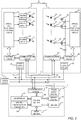
- Fig. 1 is a schematic diagram for a data processing device for a multiple optical axis photoelectric sensor according to the first embodiment.
- the multiple optical axis photoelectric sensor S has a light projecting section 1 in which a plurality of light projecting elements 11 are arranged and a light receiving section 2 in which the same number of light receiving elements 21 as that of the light projection elements 11 are arranged so that each projection surface of the light projecting elements and each light receiving surface of light receiving elements faces each other.
- the light projecting section 1 includes a driving circuit 12 that drives each of light projecting elements 11 individually, an optical axis sequential selecting circuit 13, a control circuit 16, a communication circuit 17, a power supply circuit 18, etc., in addition to the light projecting elements 11.
- the light receiving section 2 includes an amplifier 22 and an analog 23 for each of the light receiving elements 21, an optical axis sequential selecting circuit 25, a control circuit 26, an inputting amplifier 24 to the control circuit 26, a communication circuit 27, a power supply circuit 28, etc., in addition to the light receiving elements 21.
- Each of the control circuits 16, 26 in the light projecting section 1 and the light receiving section 2 is comprised of a micro computer including a CPU and a memory, for example.
- Each of the communication circuits 17, 27 is a communication interface conforming to RS485, so that it controls the exchanging of signals between the light projecting section 1 and the light receiving section 2 through two communication lines 6A, 6B corresponding to RS485.
- Each of the power supply circuits 18, 28 receives the power supply from a common external power source 5 (DC power supply), so that it supplies the power supply to each section in the device (in the light projecting section 1 and the light receiving section 2).
- the power supply lines are branched to two power supply lines 7A, 7B. One is connected to the power supply circuit 18 in the light projecting section 1, while another is connected to the power supply circuit 28 in the light projecting section 2. Then, the power supply from the external power source 5 to each of the power supply circuits 18, 28 is executed through the power supply lines 7A, 7B. Therefore, the light projecting section 1 is in the state of connecting to the light receiving section 2 with the communication lines 6A, 6B and the power supply lines 7A, 7B.
- the control circuit 16 in the light projecting section 1 generates timing signals every prescribed time to provide them to the optical axis sequential selecting circuit 13.
- the optical axis sequential selecting circuit 13 is a gate circuit for connecting each drive circuit 12 of each of the light projecting elements 11 to the control circuit 16 sequentially.
- the timing signal from the control circuit 16 is sequentially provided to each drive circuit 12, so that a sequential light emitting operation in each of the light projecting elements 11 is implemented.
- the timing signal is also provided to the control circuit 26 in the light receiving section 2 through the communication circuits 17, 27.
- the output from each of the light receiving elements 21 (hereinafter referred to "light receiving output”) is transmitted to an input line 29 to the control circuit 26 through the amplifier 22 and the analog switch 23.
- the control circuit 26 transmits the timing signal from the light projecting section 1 to the optical axis sequential selecting circuit 25 to turn on each analog switch 23 in each optical axis sequentially. Then, the control circuit 26 receives the light receiving output from the light receiving element 21 corresponding to the light projecting element which emits light, so that it compares each light receiving output with a predetermined threshold value to determine whether or not each optical axis is in a shielded stated.
- control circuit 26 When the receiving of the light receiving output is finished for all optical axes, the control circuit 26 performs a final determining process by collecting the determining result for each optical axis to produce an object detecting signal. Then the control circuit 26 outputs the object detecting signal to an external through an output circuit which is not described in drawings.
- a branch connector 4 the communication lines 6A, 6B and the power supply lines 7A, 7B are branched to an external, a data processing device 3 as a data processing device of the multiple optical axis photoelectric sensor S can be connected between the light projecting section 1 and the light receiving section 2.
- the data processing device 3 can set the definition of various detecting operations, such as a fixed blanking function, a floating blanking, etc., by putting the multiple optical axis photoelectric sensor S before it operates to a setting mode. Furthermore, the data processing device 3 can backup setting data in the multiple optical axis photoelectric sensor S, and can restore the setting data for a changed multiple optical axis photoelectric sensor S.
- Fig. 2 is a diagram showing the appearance of the data processing device 3.
- a DIP switch 31 as a setting section
- a push switch 32 as a confirming switch
- an LED 33 and a USB terminal 34 which can be connected to an external computer are provided.
- the LED 33 includes an IN-LED 33A, an OUT-LED 33B, and an ERR-LED 33C. The function of these LEDs will be described later.
- a connecting terminal 35A for connecting to the light projecting section 1 a connecting terminal 35B for connecting to the light receiving section 2
- a connecting terminal 35C for connecting to IO-LINK (registered trademark) a connecting terminal 35D for connecting to IO-LINK (registered trademark)
- IO-LINK registered trademark
- a memory 37 as a storing section, a communication section 38, a USB interface 39, a power supply section 40, a display section 41, an input section 42, and a generic communication transceiver 43 as a generic communication section are included in addition to a control section 36 comprised of a micro computer.
- the communication section 38 is an interface conforming to RS485 standard as well as the communication circuits in the light projection section 1 and the light receiving section 2.
- the communication section 38 is connected to the communication lines 6A, 6B branched by the branch connector 4.
- the power supply section 40 is connected to the power supply lines 7A, 7B branched by the branch connector 7 to supply power to each section in the data processing device 3 by receiving power from the external power supply 5.
- the USB interface 39 enables to communicate between the control section 36 and an personal computer when the personal computer is connected to the USB terminal 34.
- the communicating function using Bluetooth (registered trademark) may be provided for the communication with the personal computer.
- the data processing device 3 can be driven only by the bus power in a personal computer.
- the display section 41 is an interface for displaying, so that it performs the control for turning on the LED 33.
- Input section 42 is an input interface that accepts the input by the DIP switch 31 and the push switch 32 to transmit the contents of the input to the control section 36.
- the generic communication transceiver 43 has the function of converting a communication protocol to disclose the information of the multiple optical axis photoelectric sensor S to a generic system by IO-LINK. Thus, it is possible to improve efficiency in trouble-shooting and information collection for a safety system.
- the control section 36 is comprised of a CPU.
- the memory 37 is comprised of a flash ROM, for example, in which a program and setting data described later, etc., are stored.
- the control section 36 reads in the input of the DIP switch 31 and the push switch 32 through the input section 42 to set the definition of various detecting operations to the sensor S by the communication between the light projecting section 1 and the light receiving section 2.
- the control section 36 backups the current setting data in the sensor S, and restores the setting data to a changed new sensor S.
- the result of the detecting process is incorporated in the light receiving section 2, so that the result is set to the light receiving section 2 after performing an invalidation process for optical axes, etc.
- the data processing device 3 is configured to be able to rewrite a program of the control section 36 and the setting data in the sensor S appropriately so that it can be used continuously even when a program for setting is modified, or a new type of sensor is released.
- the data processing device 3 is connected to a personal computer (undescribed in drawings) including electric data for updating, etc., through the USB interface 39. Then, the setting data is rewritten in the data processing device 3 by the personal computer. Next, by connecting the data processing device 3 to the sensor S, the setting data to the sensor S is updated under the determination of the data processing device 3.
- the same setting data for a certain sensor S1 may be used for another sensor S2.
- the setting data for the certain sensor S1 is backuped in the data processing device 3 under the determination of the data processing device 3.
- the setting data is restored in the other sensor S2 under the determination of the data processing device 3.
- the data processing device 3 can perform the process alone by connecting the data processing device 3 to the sensor S.
- the setting data can be written in the sensor S under the determination of the data processing device 3 by connecting the data processing device 3 to the sensor S.
- the DIP switch 31 is provided as a setting section for setting the above-mentioned operating conditions of the data processing device 3.
- Fig. 3 is a diagram showing a part of the functions of the DIP switch 31.
- the DIP switch having eight channels is used.
- a channel 1 is used for switching "LOCK” and "UNLOCK".
- the channel 1 is set to "UNLOCK.” If the channel is set to "UNLOCK”, the data written in the data processing device 3 in in uncertain condition, so that it is possible to backup the setting data. If the channel 1 is set to "LOCK”, the data written in the data processing device 3 is in determined condition, so that it is possible to restore the setting data. It can be said that the channel 1 is a switch for switching a backuping operation and a restoring operation.
- a channel 2 is used for switching "DIP ENABLE” and "DIP DISABLE.”
- the channel 2 is set to "DIP DISABLE.” If the channel 2 is set to "DIP DISABLE", the setting by the DIP switch 31 is disabled, so that the setting written in the data processing device 3 by a personal computer is enabled. If the channel 2 is set to "DIP ENABLE”, the setting by the DIP switch 31 is enabled, the information written by the personal computer is overwritten with the information set by the DIP switch 31. Therefore, it is possible to set the operation of the sensor S in the data processing device 3 alone.
- a channel 3 is used for switching the functions of EDM (External Device Monitoring) .
- EDM External Device Monitoring
- the channel 3 is set to "EDM Disabled", so that EDM is disabled. If EDM is enabled, the monitoring of a relay contact, etc., is performed by the sensor S.
- a channel 4 and a channel 5 are used for switching "Auto Reset” and "Manual Reset.”
- the channel 4 and the channel 5 are set to "Auto Reset.” If they are set to "Auto Reset”, an safety output is output when the sensor S confirms that the operations of receiving light are done in all optical axes. If they are set to "Manual Reset", the safety output is output after a user's operation even when the sensor S confirms that the operations of receiving light are done in all optical axes.
- the data processing device 3 As described above, the data processing device 3 according to the present embodiment, it is possible to change the setting of the operations of the sensor 3 in the data processing device 3 alone by setting the DIP switch 31.
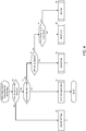
- the control section 36 in the data processing device 3 determines whether or not the data processing device 3 is connected to the sensor S (S1). If the control section 36 determines that the data processing device 3 is not connected to the sensor 3 (S1:NO), the control section 36 receives setting data, etc. from a personal computer to perform updating the setting data of the memory 37, etc., since it is determined that the data processing device 3 is connected to the personal computer (S2) .
- control section 36 determines whether this data processing device 3 is in the state of factory shipment and used for the first time, or it already has a used history (S3). It is possible to determine whether it is used for the first time or not since any data for any sensor S is not stored in the memory 37.
- control section 36 determines that this data processing device 3 is used for the first time (S3:YES), it performs backuping process forcibly (S4). If the control section 36 determines that this data processing device 3 is not used for the first time and has a use history (S3:NO), it determines whether or not the channel 1 of the DIP switch 31 is set to "UNLOCK” (S5). If the control section 36 determines that the channel 1 of the DIP switch 31 is set to "UNLOCK” (S5:YES), it performs the backuping process (S6).
- control section 36 determines whether or not the setting data read out from the sensor S connected to the data processing device 3 coincides with the setting data stored in the data processing device 3 (S7).
- the setting data is one for the type of the sensor S, the number of optical axes, the distance of an axis, etc.
- control section 36 determines that the data processing device 3 is connected to a new sensor 3 since the setting data does not coincide with that stored in the data processing device 3 (S7:NO), it performs a restoring process (S8). However, if the control section 36 determines that the data processing device 3 is connected to the same sensor 3 as that connected to so far since the setting data coincides with that stored in the data processing device 3 (S7:YES), it performs a normal process (a sensor detecting operation) without changing the setting data in the sensor S (S9).
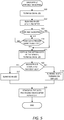
- Fig. 5 shows the details of a forcible backuping process indicated in the step S4 of Fig.4 and a backuping process indicated in the step S6 of Fig.4 .
- control section 36 turns on the IN-LED 33A when the forcible backuping process or the backuping process is started (S10).
- the control section 36 makes the IN-LED 33A blink at a slow speed (S12).
- the control section 36 determines whether the buckuping process is a forcible one or a normal one (S13). As described above, if any data of any sensor S is not stored in the memory 37, the control section 36 can determine that it is a forcible backuping process. If the control section 36 determines that it is a forcible backuping process (S13:YES), it copies the setting data in the sensor S and the setting data in the data processing device 3 to the memory 37 (S15) to turn on the IN-LED 33A. If it is a forcible backuping process, the forcible backuping process is implemented just by connecting the data processing device 3 to the sensor S.
- control section 36 determines whether or not the push switch 32 is pressed more than one second (S14). This is because it prevents user's undesired rewriting of data in the data processing device 3 from being implemented. Although this is not described in Fig. 5 , if the control section 36 cannot confirm that the push switch 32 is pressed more than one second even after a predetermined period, it may suspend a process.
- control section 36 determines that the push switch 32 is pressed more than one second (S14:YES), it copies the setting data in the sensor S to the memory 37 (S15) to turn on the IN-LED 33A (S15).
- the control section 36 determines whether or not the buckuping process is completed successfully (S16). If the control section 36 determines that the buckuping process is completed successfully (S16:YES), it makes the IN-LED 33A blink (S17). If the control section 36 determines that the buckuping process is not completed successfully (S16:NO), it makes the IN-LED 33A blink and makes the ERR-LED 33C turn on (S18) .
- Fig. 6 shows the details of a restoring process indicated in the step S8 of Fig. 4 .
- control section 36 makes the OUT-LED 33B turn on when the restoring processing is started (S20).
- the control section 36 makes the OUT-LED 33B at a slow speed (S22).
- the control section 36 determines whether the basic information of the connected sensor S coincides with the basic information stored in the data processing device 3 (S23).
- the basic information includes a CRC of setting data group and a connecting configuration of a sensor S.
- the setting data group includes a type of a sensor S, the number of optical axes, a distance between optical axes, etc.
- control section 36 determines that the basic information of the connected sensor S coincides with the basic information stored in the data processing device 3 (S23:YES), it copies the setting data stored in the memory 37 in the data processing device 3 to the sensor S to make the OUT-LED 33A turn on (S26) .
- the restoring process when the basic information coincides with the basic information stored in the data processing device 3, the restoring process is automatically implemented just by connecting the data processing device 3 to the sensor S.
- control section 36 determines whether or not only the number of optical axes of the sensor S is different from that in the basic information stored in the data processing device 3 (S24). This is because there is a case where the restoring process is implemented with respect to the sensor S, in which only the number of optical axes is different, according to the user's determination. If the control section 36 determines that only the number of the optical axes in the sensor S is different from that in the basic information stored in the data processing device 3 (S24:YES), it determines whether or not the push switch 32 is pressed more than one second (S26) .
- control section 36 may suspend a process.
- control section 36 determines that the push switch 32 is pressed more than one second (S26:YES), it copies the setting data stored in the memory 37 of the data processing device 3 to the sensor S to make the OUT-LED 33B turn on (S37).
- control section determines that not only the number of optical axes of the sensor S, but also other information is different from those in the basic information stored in the data processing device 3 (S24:NO), it makes the IN-LED 33A and the OUT-LED 33B blink, and makes the ERR-LED 33C turn on since it is inappropriate to implement the restoring process.
- the control section 36 determines whether or not the restoring process is completed successfully after the copy of the setting data from the data processing device 3 to the sensor S indicated in the step S27 is completed (S28) . If the control section 36 determines that the restoring process is completed successfully (S28:YES), it makes the OUT-LED 33B blink (S29). If the control section 36 determines that the restoring process is not completed successfully (S28:NO), it makes the OUT-LED 33B blink, and makes the ERR-LED 33C turn on (S30).
- the data processing device 3 is removed from the sensor S (S31). Although this is not described in Fig. 6 , the data processing device 3 may be restarted without removing the data processing device 3 from the sensor S.
- a backuping process and a restoring process are implemented according to the determination by the data processing device 3 just by connecting the data processing device 3 to the sensor S. Therefore, it is possible for anyone to easily implement the backuping process and the restoring process without bringing a personal computer, etc., to a production site.
- the data processing device 3 is connected to one sensor S.
- the data processing device 3 may implement the above-described backuping process and restoring process with respect to a plurality of sensors S by securing memory areas for the plurality of sensors S in the memory 37 and distinguishing each of the plurality of sensors S.
- the restoring process may be automatically implemented just when the sensor 3 is connected to the data processing device 3 if only the same type of light projecting section 1, or only the same type of light receiving section 2 is exchanged.
- the senor S may be operated on the basis of data after the restoring process by automatically restarting the sensor S after the data processing device 3 implements the restoring process.
Landscapes
- Physics & Mathematics (AREA)
- General Physics & Mathematics (AREA)
- Engineering & Computer Science (AREA)
- Computer Security & Cryptography (AREA)
- Life Sciences & Earth Sciences (AREA)
- General Life Sciences & Earth Sciences (AREA)
- Geophysics (AREA)
- Electronic Switches (AREA)
- Geophysics And Detection Of Objects (AREA)
- Photometry And Measurement Of Optical Pulse Characteristics (AREA)
- Switches Operated By Changes In Physical Conditions (AREA)
Abstract
Description
- The present disclosure relates to a data processing device for a multiple optical axis photoelectric sensor.
- In general, a multiple optical axis photoelectric sensor has a light projecting section in which a plurality of light projecting elements are arranged in a raw and a light receiving section in which the same number of light receiving elements as that of the light projection elements are arranged in a raw so that each of the light projecting elements and each of light receiving elements faces each other on one-to-one basic. The light projecting section is connected to the light receiving section through a communication line. When light is sequentially emitted from each of the light projecting elements in the light projecting section, a certain amount of light, which is received by each of the light receiving elements corresponding to each of the light projecting elements in the light receiving section at a timing synchronized with the light emitting operation in each of the light projecting elements, is extracted in the light projecting section. Thus, the o is detected sequentially. Furthermore, in the light receiving section, on the basis of the detecting result of the shielded state for each optical axis, it is determined whether or not there is an object in an detecting area, so that the light receiving section outputs a signal indicating the detecting result (hereinafter referred to "an object detecting signal").
- This kind of sensor is usually set so that the object detecting signal is turned on when the shielded state is detected in any one of optical axes. However, depending on the place of installation of the sensor or the purpose of the use of the sensor, there are cases where various conditions have to be set for the contents of detecting operations, such as invalidating the detecting result in a certain optical axis, turning on the object detecting signal only when optical axes of a prescribed number or more are shielded, etc.
- For example, the following
Patent Literature 1 discloses the technology in which various conditions are set by a console connected to a sensor. - Patent Literature 1: Japanese Unexamined Patent Application Publication No.
2002-296361 - However, in the
Patent Literature 1, if it is necessary to copy the setting of the various conditions in a certain sensor needs to another sensor, a user has to connect a console connecting to the other sensor to a personal computer to perform the same setting as that of the various conditions in the certain sensor with respect to the console connected to the other sensor. - In the
Patent Literature 1, since it is necessary to connect a personal computer to a console directly in order to change the setting, a user has to bring the personal computer to a production site when copying the setting of the various conditions in a certain sensor to another sensor. Therefore, the user's operation is complicated. Furthermore, in some cases, it is impossible for everyone to perform the copy of the setting since a user having use authority for the personal computer is limited. Moreover, if different settings are needed for a plurality of sensors respectively, a user has to perform the different settings. Therefore, it is complicated. - The objects of the present invention is to provide a data processing device for a multiple optical axis photoelectric sensor in which anyone can easily perform the backuping of the setting data for the multiple optical axis photoelectric sensor and the restoring of the setting data.
- To solve the above-described problem, a data processing device that is capable of being connected to a multiple optical axis photoelectric sensor for detecting a shielded state for each of a plurality of optical axes to output a signal indicating presence or absence of an object on the basis of a result of detecting the shielded state, and is capable of reading and writing data including setting data for setting definitions of detecting operations at the multiple optical axis photoelectric sensor, in which the data processing device for the multiple optical axis photoelectric sensor includes: a communication section that is capable of communicating with the multiple optical axis photoelectric sensor; a storing section that is capable of storing the setting data and product information of the multiple optical axis photoelectric sensor; a setting section for setting operating conditions of the data processing device; and a control section for controlling an operation of the data processing device, in which the control section reads the setting data from the multiple optical axis photoelectric sensor through the communication section to store the setting data read from the multiple optical axis photoelectric sensor in the storing section, or writes the setting data, which is stored in the storing section, in the multiple optical axis photoelectric sensor through the communication section, according to a state of connection with the multiple optical axis photoelectric sensor, a use history of the data processing device, the operating conditions set by the setting section, and the product information.
- The data processing device for the multiple optical axis photoelectric sensor reads the setting data from the multiple optical axis photoelectric sensor through the communication section to store the setting data read from the multiple optical axis photoelectric sensor in the storing section, according to a state of connection with the multiple optical axis photoelectric sensor, a use history of the data processing device, the operating conditions set by the setting section, and the product information. Furthermore, the data processing device for the multiple optical axis photoelectric sensor writes the setting data stored in the storing section in the multiple optical axis photoelectric sensor through the communication section, according to a state of connection with the multiple optical axis photoelectric sensor, a use history of the data processing device, the operating conditions set by the setting section, and the product information.
- According to the data processing device for the multiple optical axis photoelectric sensor, it performs the buckuping process or the restoring process of the setting data in multiple optical axis photoelectric sensor according to the determination of each condition just by connecting the data processing device to the multiple optical axis photoelectric sensor. Therefore, for example, if the multiple optical axis photoelectric sensor is exchanged, it is possible to implement the resetting of the multiple optical axis photoelectric sensor just by connecting the data processing device to the multiple optical axis photoelectric sensor.
- In one aspect of the data processing device for the multiple optical axis photoelectric sensor, the control section performs reading or writing of the setting data if the control section determines that the data processing device is in a state of connecting to the multiple optical axis photoelectric sensor.
- According to the one aspect of the data processing device for the multiple optical axis photoelectric sensor, the data processing device performs the reading or writing of the setting data if it determines that the data processing device is in a state of connecting to the multiple optical axis photoelectric sensor. Therefore, it is possible to easily performs the resetting of the multiple optical axis photoelectric sensor just by connecting to the data processing device to the multiple optical axis photoelectric sensor.
- In another aspect of the data processing device for the multiple optical axis photoelectric sensor, the control section forcibly performs the reading of the setting data if the control section determines that the data processing device does not have a use history of the data processing device.
- According to the other aspect of the data processing device for the multiple optical axis photoelectric sensor, the reading of the setting data is performed forcibly if the control section determines that the data processing device has no use history at a state of the factory shipment. Thus, it is possible to easily perform the buckuping process for the multiple optical axis photoelectric sensor just by connecting the data processing device to the multiple optical axis photoelectric sensor.
- In other aspect of the data processing device for the multiple optical axis photoelectric sensor, the control section performs the reading of the setting data if the control section determines that thee data processing device has a use history of the data processing device, and if the reading of the setting data is set to be enabled by the setting section.
- According to the other aspect of the data processing device for the multiple optical axis photoelectric sensor, the setting section can set whether or not the reading of the setting data is enabled. If the data processing device has a use history of the data processing device, it indicates that any one of the forcible reading of the setting data or the intentional reading of the setting data has been performed at least once so far. Therefore, in this case, the setting data of the multiple optical axis photoelectric sensor is stored in the storing section. However, if a user sets that the reading of the setting data is enabled using the setting section, the control section prioritizes the user's intention, so that it easily performs the backuping process just before connecting the data processing device to the multiple optical axis photoelectric sensor.
- In the other aspect of data processing device for the multiple optical axis photoelectric sensor, the data processing device further includes a confirming switch. The control section performs the reading of the setting data after the control section confirms that the confirming switch is pressed by a user.
- According to the other aspect of data processing device for the multiple optical axis photoelectric sensor, since the reading of the setting data is performed after the pressing of the confirming switch is confirmed, it is possible to prevent a user's undesired overwriting of the setting data in the data processing device from being implemented.
- In the other aspect of data processing device for the multiple optical axis photoelectric sensor, the control section performs the writing of the setting data if the control section determines that the data processing device has a use history of the data processing device, and if the reading of the setting data is set to be disabled by the setting section, and if product information of the multiple optical axis photoelectric sensor does not coincide with that stored in the storing section.
- According to the other aspect of data processing device for the multiple optical axis photoelectric sensor, the setting section can set whether or not the reading of the setting data is disabled. If the data processing device has a use history of the data processing device, the setting data is stored in the storing section. Therefore, if a user exchanges the multiple optical axis photoelectric sensor and sets that the reading of the setting data is disabled using the setting section, it easily performs the restoring process just before connecting the data processing device to the exchanged multiple optical axis photoelectric sensor.
- In the other aspect of data processing device for the multiple optical axis photoelectric sensor, the data processing device further includes a confirming switch. The control section performs the writing of the setting data after the control section confirms that the confirming switch is pressed by a user.
- According to the other aspect of data processing device for the multiple optical axis photoelectric sensor, since the writing of the setting data is performed after the pressing of the confirming switch is confirmed, it is possible to a user's undesired overwriting in the multiple optical axis photoelectric sensor from being implemented.
- In the other aspect of data processing device for the multiple optical axis photoelectric sensor, the control section makes the multiple optical axis photoelectric sensor operate using the setting data after the writing of the setting data is performed, by restarting the multiple optical axis photoelectric sensor after performing the writing of the setting data.
- According to the other aspect of data processing device for the multiple optical axis photoelectric sensor, after performing the writing of the setting data, the control section automatically restarts the multiple optical axis photoelectric sensor, and makes the multiple optical axis photoelectric sensor operate using the setting data after the writing of the setting data is performed. It is possible to enhance convenience.
- In the other aspect of data processing device for the multiple optical axis photoelectric sensor, a plurality of multiple optical axis photoelectric sensors are provided. The storing section is capable of storing each product information for each of the plurality of multiple optical axis photoelectric sensors. The control section performs the reading of the setting data from each of the plurality of multiple optical axis photoelectric sensors, or performs the writing of the setting data in each of the plurality of multiple optical axis photoelectric sensors.
- According to the other aspect of data processing device for the multiple optical axis photoelectric sensor, the data processing device can be connected to a plurality of multiple optical axis photoelectric sensors arranged in different places respectively. The storing section can store each product information for each of the plurality of multiple optical axis photoelectric sensors. The reading of and the writing of the setting data are performed with respect to each of the plurality of multiple optical axis photoelectric sensors. Therefore, it is possible to easily perform the backuping process and the restoring process in each of the plurality of multiple optical axis photoelectric sensors just by connecting one data processing device to the plurality of multiple optical axis photoelectric sensors.
- In the other aspect of data processing device for the multiple optical axis photoelectric sensor, the multiple optical axis photoelectric sensor includes a light projecting section and a light receiving section. The storing section is capable of storing each product information for each of the light projecting section and the light receiving section. The control section performs the reading of the setting data from each of the light projecting section and the light receiving section, or performs the writing of the setting data in each of the light projecting section and the light receiving section.
- According to the other aspect of data processing device for the multiple optical axis photoelectric sensor, the storing section can store each product information for each of the light projecting section and the light receiving section. The control section performs the reading and the writing of the setting data with respect to each of the light projecting section and the light receiving section. Therefore, if any of the light projecting section and the light receiving section is exchanged, it is possible to easily perform the backuping process and the restoring process of the multiple optical axis photoelectric sensor just by connecting the data processing device to the multiple optical axis photoelectric sensor.
- In the other aspect of data processing device for the multiple optical axis photoelectric sensor, the data processing device is capable of being connected to a plurality of light projecting sections and a plurality of light receiving sections. The storing section is capable of storing each product information for each of the plurality of light projecting sections and each of the plurality of light receiving sections. The control section performs the reading of the setting data from each of the plurality of light projecting sections and each of the plurality of light receiving sections, or performs the writing of the setting data in each of the plurality of light projecting sections and each of the plurality of light receiving sections.
- According to the other aspect of data processing device for the multiple optical axis photoelectric sensor, if a plurality of light projecting sections and a plurality of light receiving sections are connected to the data processing device, the storing section can store each product information for each of the plurality of light projecting sections and each of the plurality of light receiving sections. The reading and writing of the setting are performed with respect to each of the plurality of light projecting sections and each of the plurality of light receiving sections. Therefore, if any of the plurality of light projecting sections and the plurality of light receiving sections is exchanged, it is possible to easily perform the backuping process and the restoring process of the multiple optical axis photoelectric sensor just by connecting the data processing device to the multiple optical axis photoelectric sensor.
- In the other aspect of data processing device for the multiple optical axis photoelectric sensor, the data processing device further includes a generic communication section that is capable of communicating with other devices. The control section can transmit data stored in the storing section to the other device through the generic communication section.
- According to the other aspect of data processing device for the multiple optical axis photoelectric sensor, the other device can be connected to the data processing device. The data such as the setting data stored in the storing section can be transmitted to the other device through the generic communication section. Thus, it is possible to improve efficiency in trouble-shooting and information collection for a safety system.
- In the other aspect of data processing device for the multiple optical axis photoelectric sensor, the data processing device is capable of being driven only by a bus power in a personal computer.
- According to the other aspect of data processing device for the multiple optical axis photoelectric sensor, if the data processing device is connected to a USB terminal of a personal computer, etc., the data processing device can be driven only by a bus power in the personal computer. Thus, it is possible to enhance convenience.
- As described above clearly, according to the data processing device for the multiple optical axis photoelectric sensor, it is possible for anyone to easily perform the backuping process and the restoring process of the multiple optical axis photoelectric sensor.
-
-
Fig. 1 is a schematic diagram for a data processing device for a multiple optical axis photoelectric sensor according to the first embodiment; -
Fig. 2 is a diagram showing the appearance of the data processing device; -
Fig. 3 is a diagram for explaining the function of a DIP switch; -
Fig. 4 is a diagram for explaining the whole processing in the data processing device; -
Fig. 5 is a flowchart for a backuping process in the data processing device; and -
Fig. 6 is a flowchart for a restoring processing in the data processing device. - In the following, embodiments will be described in detail with reference to the drawings as appropriate.
-
Fig. 1 is a schematic diagram for a data processing device for a multiple optical axis photoelectric sensor according to the first embodiment. As shown inFig. 1 , the multiple optical axis photoelectric sensor S has alight projecting section 1 in which a plurality of light projectingelements 11 are arranged and alight receiving section 2 in which the same number of light receivingelements 21 as that of thelight projection elements 11 are arranged so that each projection surface of the light projecting elements and each light receiving surface of light receiving elements faces each other. Thelight projecting section 1 includes a drivingcircuit 12 that drives each oflight projecting elements 11 individually, an optical axis sequential selectingcircuit 13, acontrol circuit 16, acommunication circuit 17, apower supply circuit 18, etc., in addition to thelight projecting elements 11. Thelight receiving section 2 includes anamplifier 22 and ananalog 23 for each of thelight receiving elements 21, an optical axis sequential selectingcircuit 25, acontrol circuit 26, an inputtingamplifier 24 to thecontrol circuit 26, acommunication circuit 27, apower supply circuit 28, etc., in addition to thelight receiving elements 21. - Each of the
control circuits light projecting section 1 and thelight receiving section 2 is comprised of a micro computer including a CPU and a memory, for example. Each of thecommunication circuits section 1 and thelight receiving section 2 through twocommunication lines - Each of the
power supply circuits light projecting section 1 and the light receiving section 2). The power supply lines are branched to twopower supply lines power supply circuit 18 in thelight projecting section 1, while another is connected to thepower supply circuit 28 in thelight projecting section 2. Then, the power supply from theexternal power source 5 to each of thepower supply circuits power supply lines light projecting section 1 is in the state of connecting to thelight receiving section 2 with thecommunication lines power supply lines - The
control circuit 16 in thelight projecting section 1 generates timing signals every prescribed time to provide them to the optical axis sequential selectingcircuit 13. The optical axis sequential selectingcircuit 13 is a gate circuit for connecting eachdrive circuit 12 of each of thelight projecting elements 11 to thecontrol circuit 16 sequentially. By the switching process in this circuit, the timing signal from thecontrol circuit 16 is sequentially provided to eachdrive circuit 12, so that a sequential light emitting operation in each of thelight projecting elements 11 is implemented. Furthermore, the timing signal is also provided to thecontrol circuit 26 in thelight receiving section 2 through thecommunication circuits - In the light receiving section, the output from each of the light receiving elements 21 (hereinafter referred to "light receiving output") is transmitted to an
input line 29 to thecontrol circuit 26 through theamplifier 22 and theanalog switch 23. Thecontrol circuit 26 transmits the timing signal from thelight projecting section 1 to the optical axis sequential selectingcircuit 25 to turn on eachanalog switch 23 in each optical axis sequentially. Then, thecontrol circuit 26 receives the light receiving output from thelight receiving element 21 corresponding to the light projecting element which emits light, so that it compares each light receiving output with a predetermined threshold value to determine whether or not each optical axis is in a shielded stated. When the receiving of the light receiving output is finished for all optical axes, thecontrol circuit 26 performs a final determining process by collecting the determining result for each optical axis to produce an object detecting signal. Then thecontrol circuit 26 outputs the object detecting signal to an external through an output circuit which is not described in drawings. - In the first embodiment, by a
branch connector 4, thecommunication lines power supply lines data processing device 3 as a data processing device of the multiple optical axis photoelectric sensor S can be connected between the light projectingsection 1 and thelight receiving section 2. - The
data processing device 3 can set the definition of various detecting operations, such as a fixed blanking function, a floating blanking, etc., by putting the multiple optical axis photoelectric sensor S before it operates to a setting mode. Furthermore, thedata processing device 3 can backup setting data in the multiple optical axis photoelectric sensor S, and can restore the setting data for a changed multiple optical axis photoelectric sensor S. -
Fig. 2 is a diagram showing the appearance of thedata processing device 3. In the front face of the housing of thedata processing device 3, aDIP switch 31 as a setting section, apush switch 32 as a confirming switch, anLED 33, and aUSB terminal 34 which can be connected to an external computer are provided. TheLED 33 includes an IN-LED 33A, an OUT-LED 33B, and an ERR-LED 33C. The function of these LEDs will be described later. - In the side face of the housing, a connecting terminal 35A for connecting to the
light projecting section 1, a connecting terminal 35B for connecting to thelight receiving section 2, a connecting terminal 35C for connecting to IO-LINK (registered trademark), and apower supply terminal 35D are provided. - As shown in
Fig. 1 , inside the housing of thedata processing device 3, amemory 37 as a storing section, acommunication section 38, aUSB interface 39, apower supply section 40, a display section 41, aninput section 42, and ageneric communication transceiver 43 as a generic communication section are included in addition to acontrol section 36 comprised of a micro computer. - The
communication section 38 is an interface conforming to RS485 standard as well as the communication circuits in thelight projection section 1 and thelight receiving section 2. Thecommunication section 38 is connected to thecommunication lines branch connector 4. Thepower supply section 40 is connected to thepower supply lines branch connector 7 to supply power to each section in thedata processing device 3 by receiving power from theexternal power supply 5. - The
USB interface 39 enables to communicate between thecontrol section 36 and an personal computer when the personal computer is connected to theUSB terminal 34. The communicating function using Bluetooth (registered trademark) may be provided for the communication with the personal computer. Thedata processing device 3 can be driven only by the bus power in a personal computer. - The display section 41 is an interface for displaying, so that it performs the control for turning on the
LED 33.Input section 42 is an input interface that accepts the input by theDIP switch 31 and thepush switch 32 to transmit the contents of the input to thecontrol section 36. - The
generic communication transceiver 43 has the function of converting a communication protocol to disclose the information of the multiple optical axis photoelectric sensor S to a generic system by IO-LINK. Thus, it is possible to improve efficiency in trouble-shooting and information collection for a safety system. - The
control section 36 is comprised of a CPU. Thememory 37 is comprised of a flash ROM, for example, in which a program and setting data described later, etc., are stored. Thecontrol section 36 reads in the input of theDIP switch 31 and thepush switch 32 through theinput section 42 to set the definition of various detecting operations to the sensor S by the communication between the light projectingsection 1 and thelight receiving section 2. Thecontrol section 36 backups the current setting data in the sensor S, and restores the setting data to a changed new sensor S. - According to the above-mentioned configuration, by incorporating interfaces conforming to RS485 standard in the
communication circuits light projection section 1 and thelight receiving section 2, and thecommunication section 38 in thedata processing device 3, a bidirectional communication is performed individually between various sections. Therefore, in thedata processing device 3, it is possible to perform the setting process individually with respect to any of thelight projection section 1 and thelight receiving section 2. Although most of definitions relating to an object detecting are set in thecontrol circuit 26 in thelight receiving section 2, the definition of a process, in which an actual result of the detecting process needs to be registered, such as a fix blanking, is set in thelight receiving section 2. In this case, by transmitting a command to thelight projecting section 1 to let thelight receiving section 2 perform a projection operation, the result of the detecting process is incorporated in thelight receiving section 2, so that the result is set to thelight receiving section 2 after performing an invalidation process for optical axes, etc. - The
data processing device 3 is configured to be able to rewrite a program of thecontrol section 36 and the setting data in the sensor S appropriately so that it can be used continuously even when a program for setting is modified, or a new type of sensor is released. - To perform this rewriting process, first, the
data processing device 3 is connected to a personal computer (undescribed in drawings) including electric data for updating, etc., through theUSB interface 39. Then, the setting data is rewritten in thedata processing device 3 by the personal computer. Next, by connecting thedata processing device 3 to the sensor S, the setting data to the sensor S is updated under the determination of thedata processing device 3. - The same setting data for a certain sensor S1 may be used for another sensor S2. In this case, by connecting the certain sensor S1 to the
data processing device 3, the setting data for the certain sensor S1 is backuped in thedata processing device 3 under the determination of thedata processing device 3. After that, by connecting thedata processing device 3 to the other sensor S2, the setting data is restored in the other sensor S2 under the determination of thedata processing device 3. - As for an easy process, such as a change of type of reset, the
data processing device 3 can perform the process alone by connecting thedata processing device 3 to the sensor S. As for a complicated setting, if the setting data is written in thedata processing device 3 by a personal computer once, the setting data can be written in the sensor S under the determination of thedata processing device 3 by connecting thedata processing device 3 to the sensor S. - In the
data processing device 3 according to the present embodiment, theDIP switch 31 is provided as a setting section for setting the above-mentioned operating conditions of thedata processing device 3.Fig. 3 is a diagram showing a part of the functions of theDIP switch 31. - In the present embodiment, the DIP switch having eight channels is used. As shown in
Fig. 3 , achannel 1 is used for switching "LOCK" and "UNLOCK". At the time of shipment of thedata processing device 3 from the factory, thechannel 1 is set to "UNLOCK." If the channel is set to "UNLOCK", the data written in thedata processing device 3 in in uncertain condition, so that it is possible to backup the setting data. If thechannel 1 is set to "LOCK", the data written in thedata processing device 3 is in determined condition, so that it is possible to restore the setting data. It can be said that thechannel 1 is a switch for switching a backuping operation and a restoring operation. - As shown in
Fig. 3 , achannel 2 is used for switching "DIP ENABLE" and "DIP DISABLE." At the time of shipment of thedata processing device 3 from the factory, thechannel 2 is set to "DIP DISABLE." If thechannel 2 is set to "DIP DISABLE", the setting by theDIP switch 31 is disabled, so that the setting written in thedata processing device 3 by a personal computer is enabled. If thechannel 2 is set to "DIP ENABLE", the setting by theDIP switch 31 is enabled, the information written by the personal computer is overwritten with the information set by theDIP switch 31. Therefore, it is possible to set the operation of the sensor S in thedata processing device 3 alone. - As shown in
Fig. 3 , achannel 3 is used for switching the functions of EDM (External Device Monitoring) . At the time of shipment of thedata processing device 3 from the factory, thechannel 3 is set to "EDM Disabled", so that EDM is disabled. If EDM is enabled, the monitoring of a relay contact, etc., is performed by the sensor S. - As shown in
Fig. 3 , achannel 4 and achannel 5 are used for switching "Auto Reset" and "Manual Reset." At the time of shipment of thedata processing device 3 from the factory, thechannel 4 and thechannel 5 are set to "Auto Reset." If they are set to "Auto Reset", an safety output is output when the sensor S confirms that the operations of receiving light are done in all optical axes. If they are set to "Manual Reset", the safety output is output after a user's operation even when the sensor S confirms that the operations of receiving light are done in all optical axes. - As described above, the
data processing device 3 according to the present embodiment, it is possible to change the setting of the operations of thesensor 3 in thedata processing device 3 alone by setting theDIP switch 31. - Referring to the flowchart indicated in
Fig. 4 to Fig.6 , a backup process and a restore process by thedata processing device 3 will be described below. - The processed indicated in
Fig.4 to Fig. 6 are implemented at that time of starting thedata processing device 3. - First, as shown in
Fig. 4 , thecontrol section 36 in thedata processing device 3 determines whether or not thedata processing device 3 is connected to the sensor S (S1). If thecontrol section 36 determines that thedata processing device 3 is not connected to the sensor 3 (S1:NO), thecontrol section 36 receives setting data, etc. from a personal computer to perform updating the setting data of thememory 37, etc., since it is determined that thedata processing device 3 is connected to the personal computer (S2) . - If the
control section 36 determines that thedata processing device 3 is connected to the sensor S (S1:YES), thecontrol section 36 determines whether thisdata processing device 3 is in the state of factory shipment and used for the first time, or it already has a used history (S3). It is possible to determine whether it is used for the first time or not since any data for any sensor S is not stored in thememory 37. - If the
control section 36 determines that thisdata processing device 3 is used for the first time (S3:YES), it performs backuping process forcibly (S4). If thecontrol section 36 determines that thisdata processing device 3 is not used for the first time and has a use history (S3:NO), it determines whether or not thechannel 1 of theDIP switch 31 is set to "UNLOCK" (S5). If thecontrol section 36 determines that thechannel 1 of theDIP switch 31 is set to "UNLOCK" (S5:YES), it performs the backuping process (S6). - However, if the
control section 36 determines that thechannel 1 of theDIP switch 31 is set to "LOCK" (S5:NO), it determines whether or not the setting data read out from the sensor S connected to thedata processing device 3 coincides with the setting data stored in the data processing device 3 (S7). The setting data is one for the type of the sensor S, the number of optical axes, the distance of an axis, etc. - If the
control section 36 determines that thedata processing device 3 is connected to anew sensor 3 since the setting data does not coincide with that stored in the data processing device 3 (S7:NO), it performs a restoring process (S8). However, if thecontrol section 36 determines that thedata processing device 3 is connected to thesame sensor 3 as that connected to so far since the setting data coincides with that stored in the data processing device 3 (S7:YES), it performs a normal process (a sensor detecting operation) without changing the setting data in the sensor S (S9). -
Fig. 5 shows the details of a forcible backuping process indicated in the step S4 ofFig.4 and a backuping process indicated in the step S6 ofFig.4 . - As shown in
Fig. 5 , thecontrol section 36 turns on the IN-LED 33A when the forcible backuping process or the backuping process is started (S10). - If the sensor S detects that the
data processing device 3 is connected to the sensor S, the setting data in thedata processing device 3 is in the state of capable of being backuped. Next, thecontrol section 36 makes the IN-LED 33A blink at a slow speed (S12). - The
control section 36 determines whether the buckuping process is a forcible one or a normal one (S13). As described above, if any data of any sensor S is not stored in thememory 37, thecontrol section 36 can determine that it is a forcible backuping process. If thecontrol section 36 determines that it is a forcible backuping process (S13:YES), it copies the setting data in the sensor S and the setting data in thedata processing device 3 to the memory 37 (S15) to turn on the IN-LED 33A. If it is a forcible backuping process, the forcible backuping process is implemented just by connecting thedata processing device 3 to the sensor S. - If the
control section 36 determines that it is not a forcible backuping process (S13:NO), it determines whether or not thepush switch 32 is pressed more than one second (S14). This is because it prevents user's undesired rewriting of data in thedata processing device 3 from being implemented. Although this is not described inFig. 5 , if thecontrol section 36 cannot confirm that thepush switch 32 is pressed more than one second even after a predetermined period, it may suspend a process. - If the
control section 36 determines that thepush switch 32 is pressed more than one second (S14:YES), it copies the setting data in the sensor S to the memory 37 (S15) to turn on the IN-LED 33A (S15). - The
control section 36 determines whether or not the buckuping process is completed successfully (S16). If thecontrol section 36 determines that the buckuping process is completed successfully (S16:YES), it makes the IN-LED 33A blink (S17). If thecontrol section 36 determines that the buckuping process is not completed successfully (S16:NO), it makes the IN-LED 33A blink and makes the ERR-LED 33C turn on (S18) . - After that, the power is turned off, the
data processing device 3 is removed from the sensor S (S19). -
Fig. 6 shows the details of a restoring process indicated in the step S8 ofFig. 4 . - As shown in
Fig. 6 , thecontrol section 36 makes the OUT-LED 33B turn on when the restoring processing is started (S20). - If the sensor S detects that the
data processing device 3 is connected to the sensor S, the setting data is in the state of capable of being restored to thedata processing device 3. Thecontrol section 36 makes the OUT-LED 33B at a slow speed (S22). - The
control section 36 determines whether the basic information of the connected sensor S coincides with the basic information stored in the data processing device 3 (S23). The basic information includes a CRC of setting data group and a connecting configuration of a sensor S. The setting data group includes a type of a sensor S, the number of optical axes, a distance between optical axes, etc. - If the
control section 36 determines that the basic information of the connected sensor S coincides with the basic information stored in the data processing device 3 (S23:YES), it copies the setting data stored in thememory 37 in thedata processing device 3 to the sensor S to make the OUT-LED 33A turn on (S26) . Thus, at the restoring process, when the basic information coincides with the basic information stored in thedata processing device 3, the restoring process is automatically implemented just by connecting thedata processing device 3 to the sensor S. - If the
control section 36 determines that the basic information of the connected sensor S does not coincide with the basic information stored in the data processing device 3 (S23:NO), it determines whether or not only the number of optical axes of the sensor S is different from that in the basic information stored in the data processing device 3 (S24). This is because there is a case where the restoring process is implemented with respect to the sensor S, in which only the number of optical axes is different, according to the user's determination. If thecontrol section 36 determines that only the number of the optical axes in the sensor S is different from that in the basic information stored in the data processing device 3 (S24:YES), it determines whether or not thepush switch 32 is pressed more than one second (S26) . This is because it prevents user's undesired rewriting of data in the sensor S from being implemented. Although this is not described inFig. 6 , if thecontrol section 36 cannot confirm that thepush switch 32 is pressed more than one second even after a predetermined period, it may suspend a process. - If the
control section 36 determined that thepush switch 32 is pressed more than one second (S26:YES), it copies the setting data stored in thememory 37 of thedata processing device 3 to the sensor S to make the OUT-LED 33B turn on (S37). - If the control section determines that not only the number of optical axes of the sensor S, but also other information is different from those in the basic information stored in the data processing device 3 (S24:NO), it makes the IN-
LED 33A and the OUT-LED 33B blink, and makes the ERR-LED 33C turn on since it is inappropriate to implement the restoring process. - The
control section 36 determines whether or not the restoring process is completed successfully after the copy of the setting data from thedata processing device 3 to the sensor S indicated in the step S27 is completed (S28) . If thecontrol section 36 determines that the restoring process is completed successfully (S28:YES), it makes the OUT-LED 33B blink (S29). If thecontrol section 36 determines that the restoring process is not completed successfully (S28:NO), it makes the OUT-LED 33B blink, and makes the ERR-LED 33C turn on (S30). - After that, the power is turned off, the
data processing device 3 is removed from the sensor S (S31). Although this is not described inFig. 6 , thedata processing device 3 may be restarted without removing thedata processing device 3 from the sensor S. - As described above, according to the present embodiment, a backuping process and a restoring process are implemented according to the determination by the
data processing device 3 just by connecting thedata processing device 3 to the sensor S. Therefore, it is possible for anyone to easily implement the backuping process and the restoring process without bringing a personal computer, etc., to a production site. - In the above-described embodiment, the
data processing device 3 is connected to one sensor S. However, thedata processing device 3 may implement the above-described backuping process and restoring process with respect to a plurality of sensors S by securing memory areas for the plurality of sensors S in thememory 37 and distinguishing each of the plurality of sensors S. - Furthermore, by memorizing product information for every
light projecting section 1 and everylight receiving section 2 in thedata processing device 3, the restoring process may be automatically implemented just when thesensor 3 is connected to thedata processing device 3 if only the same type oflight projecting section 1, or only the same type oflight receiving section 2 is exchanged. - Moreover, the sensor S may be operated on the basis of data after the restoring process by automatically restarting the sensor S after the
data processing device 3 implements the restoring process. - The embodiments are described as the exemplification of the present invention. Therefore, the present invention is not limited to those embodiments. Various modifications may be made without departing from the scope and spirit of the present invention. Although each of the above-described plurality of embodiments can be established independently, it is possible to combine the plurality of embodiments. Furthermore, although each of various features in different embodiments can be established independently, it is possible to combine the various features in different embodiments.
-
- 1
- LIGHT PROJECTING SECTION
- 2
- LIGHT RECEIVING SECTION
- 3
- DATA PROCESSING DEVIE
- 4
- BRANCH CONNECTOR
- 5
- EXTERNAL POWER SOURCE
- 6A
- COMMUNICATION LINE
- 6B
- COMMUNICATION LINE
- 7A
- POWER SUPPLY LINE
- 7B
- POWER SUPPLY LINE
- 11
- LIGHT PROJECTING ELEMENT
- 12
- DRIVING CIRCUIT
- 13
- OPTICAL AXIS SEQUENTIAL SELECTING CIRCUIT
- 16
- CONTROL CIRCUIT
- 17
- COMMUNICATION CIRCUIT
- 18
- POWER SUPPLY CIRCUIT
- 21
- LIGHT RECEIVING ELEMENT
- 22
- AMPLIFIER
- 23
- ANALOG SWITCH
- 24
- INPUTTING AMPLIFIER
- 25
- OPTICAL AXIS SEQUENTIAL SELECTING CIRCUIT
- 26
- CONTROL CIRCUIT
- 27
- COMMUNICATION CIRCUIT
- 28
- POWER SUPPLY CIRCUIT
- 31
- DIP SWITCH
- 32
- PUSH SWITCH
- 33
- LED
- 33A
- IN-LED
- 33B
- OUT-LED
- 33C
- ERR-LED
- 34
- USB TERMINAL
- 35A
- CONNECTING TERMINAL
- 35B
- CONNECTING TERMINAL
- 36
- CONTROL SECTION
- 37
- MEMORY
- 38
- COMMUNICATION SECTION
- 39
- USB INTERFACE
- 40
- POWER SUPPLY SECTION
- 41
- DISPLAY SECTION
- 42
- INPUT SECTION
- S
- MULTIPLE OPTICAL AXIS PHOTOELECTRIC SENSOR
Claims (13)
- A data processing device that is capable of being connected to a multiple optical axis photoelectric sensor for detecting a shielded state for each of a plurality of optical axes to output a signal indicating presence or absence of an object on the basis of a result of detecting the shielded state, and is capable of reading and writing data including setting data for setting definitions of detecting operations at the multiple optical axis photoelectric sensor, the data processing device for the multiple optical axis photoelectric sensor comprising:a communication section that is capable of communicating with the multiple optical axis photoelectric sensor;a storing section that is capable of storing the setting data and product information of the multiple optical axis photoelectric sensor;a setting section for setting operating conditions of the data processing device; anda control section for controlling an operation of the data processing device,wherein the control section reads the setting data from the multiple optical axis photoelectric sensor through the communication section to store the setting data read from the multiple optical axis photoelectric sensor in the storing section, or writes the setting data, which is stored in the storing section, in the multiple optical axis photoelectric sensor through the communication section, according to a state of connection with the multiple optical axis photoelectric sensor, a use history of the data processing device, the operating conditions set by the setting section, and the product information.
- The data processing device for the multiple optical axis photoelectric sensor according to claim 1,
wherein the control section performs reading or writing of the setting data if the control section determines that the data processing device is in a state of connecting to the multiple optical axis photoelectric sensor. - The data processing device for the multiple optical axis photoelectric sensor according to claim 2,
wherein the control section forcibly performs the reading of the setting data if the control section determines that the data processing device does not have a use history of the data processing device. - The data processing device for the multiple optical axis photoelectric sensor according to claim 2 or 3,
wherein the control section performs the reading of the setting data if the control section determines that thee data processing device has a use history of the data processing device, and if the reading of the setting data is set to be enabled by the setting section. - The data processing device for the multiple optical axis photoelectric sensor according to claim 4,
wherein the data processing device further comprises a confirming switch,
wherein the control section performs the reading of the setting data after the control section confirms that the confirming switch is pressed by a user. - The data processing device for the multiple optical axis photoelectric sensor according to any one of claims 2 to 5,
wherein the control section performs the writing of the setting data if the control section determines that the data processing device has a use history of the data processing device, and if the reading of the setting data is set to be disabled by the setting section, and if product information of the multiple optical axis photoelectric sensor does not coincide with that stored in the storing section. - The data processing device for the multiple optical axis photoelectric sensor according to claim 6,
wherein the data processing device further comprises a confirming switch,
wherein the control section performs the writing of the setting data after the control section confirms that the confirming switch is pressed by a user. - The data processing device for the multiple optical axis photoelectric sensor according to claim 6 or 7,
wherein the control section makes the multiple optical axis photoelectric sensor operate using the setting data after the writing of the setting data is performed, by restarting the multiple optical axis photoelectric sensor after performing the writing of the setting data. - The data processing device for the multiple optical axis photoelectric sensor according to any one of claims 1 to 8,
wherein a plurality of multiple optical axis photoelectric sensors are provided,
wherein the storing section is capable of storing each product information for each of the plurality of multiple optical axis photoelectric sensors,
wherein the control section performs the reading of the setting data from each of the plurality of multiple optical axis photoelectric sensors, or performs the writing of the setting data in each of the plurality of multiple optical axis photoelectric sensors. - The data processing device for the multiple optical axis photoelectric sensor according to any one of claims 1 to 9,
wherein the multiple optical axis photoelectric sensor comprises a light projecting section and a light receiving section,
wherein the storing section is capable of storing each product information for each of the light projecting section and the light receiving section,
wherein the control section performs the reading of the setting data from each of the light projecting section and the light receiving section, or performs the writing of the setting data in each of the light projecting section and the light receiving section. - The data processing device for the multiple optical axis photoelectric sensor according to claim 10,
wherein the data processing device is capable of being connected to a plurality of light projecting sections and a plurality of light receiving sections,
wherein the storing section is capable of storing each product information for each of the plurality of light projecting sections and each of the plurality of light receiving sections,
wherein the control section performs the reading of the setting data from each of the plurality of light projecting sections and each of the plurality of light receiving sections, or performs the writing of the setting data in each of the plurality of light projecting sections and each of the plurality of light receiving sections. - The data processing device for the multiple optical axis photoelectric sensor according to any one of claims 1 to 11,
wherein the data processing device further comprises a generic communication section that is capable of communicating with other devices,
wherein the control section is capable of transmitting data stored in the storing section to the other device through the generic communication section. - The data processing device for the multiple optical axis photoelectric sensor according to any one of claims 1 to 12,
wherein the data processing device is capable of being driven only by a bus power in a personal computer.
Applications Claiming Priority (2)
| Application Number | Priority Date | Filing Date | Title |
|---|---|---|---|
| JP2018127744A JP7021610B2 (en) | 2018-07-04 | 2018-07-04 | Data processing device for multi-optical axis photoelectric sensor |
| PCT/JP2019/026692 WO2020009195A1 (en) | 2018-07-04 | 2019-07-04 | Data processing device for multiple optical axis photoelectric sensor |
Publications (3)
| Publication Number | Publication Date |
|---|---|
| EP3819677A1 true EP3819677A1 (en) | 2021-05-12 |
| EP3819677A4 EP3819677A4 (en) | 2022-04-06 |
| EP3819677B1 EP3819677B1 (en) | 2023-04-05 |
Family
ID=69059212
Family Applications (1)
| Application Number | Title | Priority Date | Filing Date |
|---|---|---|---|
| EP19831143.3A Active EP3819677B1 (en) | 2018-07-04 | 2019-07-04 | Data processing device for multiple optical axis photoelectric sensor |
Country Status (4)
| Country | Link |
|---|---|
| EP (1) | EP3819677B1 (en) |
| JP (1) | JP7021610B2 (en) |
| CN (1) | CN112368608B (en) |
| WO (1) | WO2020009195A1 (en) |
Families Citing this family (1)
| Publication number | Priority date | Publication date | Assignee | Title |
|---|---|---|---|---|
| CN116774305A (en) * | 2023-05-17 | 2023-09-19 | 深圳市志奋领科技有限公司 | Light curtain detection device and detection method thereof |
Family Cites Families (16)
| Publication number | Priority date | Publication date | Assignee | Title |
|---|---|---|---|---|
| JP2719156B2 (en) * | 1988-09-27 | 1998-02-25 | 松下電工株式会社 | Remote monitoring and control system |
| JP3477709B2 (en) | 1999-10-29 | 2003-12-10 | オムロン株式会社 | Sensor system |
| JP3965926B2 (en) | 2001-03-30 | 2007-08-29 | オムロン株式会社 | Multi-optical axis photoelectric sensor setting device |
| JP2007147533A (en) * | 2005-11-30 | 2007-06-14 | Omron Corp | SENSOR SYSTEM, SAFETY DETECTION DEVICE SETTING DEVICE, SAFETY DETECTION DEVICE SETTING METHOD, PROGRAM, AND COMPUTER-READABLE RECORDING MEDIUM |
| JP2008118226A (en) * | 2006-10-31 | 2008-05-22 | Sunx Ltd | Detection sensor, controller, and sensor system |
| JP5064197B2 (en) * | 2007-11-12 | 2012-10-31 | 株式会社 エニイワイヤ | Photoelectric sensor |
| JP5037366B2 (en) * | 2008-01-11 | 2012-09-26 | 株式会社 エニイワイヤ | Photoelectric sensor system |
| JP2012080447A (en) * | 2010-10-05 | 2012-04-19 | Fujitsu Ltd | Electronic device, power source control program, and power source control method |
| JP6167532B2 (en) * | 2013-01-25 | 2017-07-26 | オムロン株式会社 | Control device and operation method of control device |
| JP2015159385A (en) * | 2014-02-23 | 2015-09-03 | オムロン株式会社 | Photoelectric sensor |
| JP6331829B2 (en) * | 2014-02-23 | 2018-05-30 | オムロン株式会社 | Photoelectric sensor |
| JP6361192B2 (en) * | 2014-03-14 | 2018-07-25 | オムロン株式会社 | Multi-optical axis photoelectric sensor system, control method for multi-optical axis photoelectric sensor system, program, and recording medium |
| JP6320128B2 (en) * | 2014-04-02 | 2018-05-09 | アズビル株式会社 | Sensor wiring confirmation system and method |
| JP6287677B2 (en) * | 2014-08-08 | 2018-03-07 | オムロン株式会社 | Multi-axis photoelectric sensor |
| JP2016156768A (en) | 2015-02-26 | 2016-09-01 | アズビル株式会社 | Photoelectronic sensor |
| JP6518601B2 (en) | 2016-02-22 | 2019-05-22 | 株式会社キーエンス | Setting support device for optical safety sensor, setting support program, optical safety system and optical safety sensor |
-
2018
- 2018-07-04 JP JP2018127744A patent/JP7021610B2/en active Active
-
2019
- 2019-07-04 EP EP19831143.3A patent/EP3819677B1/en active Active
- 2019-07-04 WO PCT/JP2019/026692 patent/WO2020009195A1/en not_active Ceased
- 2019-07-04 CN CN201980044161.1A patent/CN112368608B/en active Active
Also Published As
| Publication number | Publication date |
|---|---|
| EP3819677A4 (en) | 2022-04-06 |
| JP7021610B2 (en) | 2022-02-17 |
| CN112368608A (en) | 2021-02-12 |
| WO2020009195A1 (en) | 2020-01-09 |
| CN112368608B (en) | 2024-07-05 |
| EP3819677B1 (en) | 2023-04-05 |
| JP2020008352A (en) | 2020-01-16 |
Similar Documents
| Publication | Publication Date | Title |
|---|---|---|
| US20160154693A1 (en) | Method for error monitoring, control and data transmission installation and control device | |
| EP3376316B1 (en) | Slave device, control method of slave device, information processing program and computer readable recording medium | |
| CN107924168B (en) | Relay device, control method of relay device, and readable recording medium | |
| JP5992775B2 (en) | Pluggable logic controller | |
| US10484198B2 (en) | Function connection unit comprising a parameter memory | |
| JP2017167593A (en) | Relay device, relay device control method, control program, and recording medium | |
| JP2017163508A (en) | Master slave control system, method for controlling master slave control system, information processing program, and recording medium | |
| EP3819677B1 (en) | Data processing device for multiple optical axis photoelectric sensor | |
| US8804750B2 (en) | Field device | |
| WO2015079725A1 (en) | Programmable controller | |
| KR20000022800A (en) | Distributed processing system and cooperation method thereof | |
| CN114008984B (en) | Computer readable storage medium and management method | |
| TWI590012B (en) | Control machine for distributed control system and distributed control basic module | |
| JPH10222430A (en) | Controller | |
| US11650571B2 (en) | Control device, control method, and control program for executing a machining program using flag indications | |
| US6412016B1 (en) | Network link bypass device | |
| JP3335016B2 (en) | Wireless address setting device | |
| KR101261022B1 (en) | Apparatus of data processing and method of setting program data thereof | |
| JP2807406B2 (en) | Remote I/O Devices | |
| JP7419851B2 (en) | lighting control system | |
| JP7696791B2 (en) | Fire alarm system | |
| CN110517475A (en) | A kind of projection device start-up control method and equipment based on power supply timing device | |
| JP5432125B2 (en) | Civil engineering machinery / equipment with a microcomputer capable of writing individual information | |
| KR20170106797A (en) | Plc module and plc system for firmware multiple download and method for firmware multiple download using the same | |
| JP2007249625A (en) | Conversion adapter |
Legal Events
| Date | Code | Title | Description |
|---|---|---|---|
| STAA | Information on the status of an ep patent application or granted ep patent |
Free format text: STATUS: THE INTERNATIONAL PUBLICATION HAS BEEN MADE |
|
| PUAI | Public reference made under article 153(3) epc to a published international application that has entered the european phase |
Free format text: ORIGINAL CODE: 0009012 |
|
| STAA | Information on the status of an ep patent application or granted ep patent |
Free format text: STATUS: REQUEST FOR EXAMINATION WAS MADE |
|
| 17P | Request for examination filed |
Effective date: 20201216 |
|
| AK | Designated contracting states |
Kind code of ref document: A1 Designated state(s): AL AT BE BG CH CY CZ DE DK EE ES FI FR GB GR HR HU IE IS IT LI LT LU LV MC MK MT NL NO PL PT RO RS SE SI SK SM TR |
|
| DAV | Request for validation of the european patent (deleted) | ||
| DAX | Request for extension of the european patent (deleted) | ||
| RAP3 | Party data changed (applicant data changed or rights of an application transferred) |
Owner name: OMRON CORPORATION |
|
| RIN1 | Information on inventor provided before grant (corrected) |
Inventor name: YAMADA, YUYA Inventor name: YAMAJI, TAKAMASA Inventor name: KIKUCHI, KEISAKU Inventor name: HASHIMOTO, MINORU |
|
| A4 | Supplementary search report drawn up and despatched |
Effective date: 20220303 |
|
| RIC1 | Information provided on ipc code assigned before grant |
Ipc: F16P 3/14 20060101ALI20220225BHEP Ipc: G08B 13/186 20060101ALI20220225BHEP Ipc: H01H 35/00 20060101ALI20220225BHEP Ipc: G01J 1/42 20060101ALI20220225BHEP Ipc: G01V 8/20 20060101AFI20220225BHEP |
|
| GRAP | Despatch of communication of intention to grant a patent |
Free format text: ORIGINAL CODE: EPIDOSNIGR1 |
|
| STAA | Information on the status of an ep patent application or granted ep patent |
Free format text: STATUS: GRANT OF PATENT IS INTENDED |
|
| GRAS | Grant fee paid |
Free format text: ORIGINAL CODE: EPIDOSNIGR3 |
|
| INTG | Intention to grant announced |
Effective date: 20230125 |
|
| GRAA | (expected) grant |
Free format text: ORIGINAL CODE: 0009210 |
|
| STAA | Information on the status of an ep patent application or granted ep patent |
Free format text: STATUS: THE PATENT HAS BEEN GRANTED |
|
| AK | Designated contracting states |
Kind code of ref document: B1 Designated state(s): AL AT BE BG CH CY CZ DE DK EE ES FI FR GB GR HR HU IE IS IT LI LT LU LV MC MK MT NL NO PL PT RO RS SE SI SK SM TR |
|
| REG | Reference to a national code |
Ref country code: GB Ref legal event code: FG4D |
|
| REG | Reference to a national code |
Ref country code: DE Ref legal event code: R096 Ref document number: 602019027309 Country of ref document: DE |
|
| REG | Reference to a national code |
Ref country code: CH Ref legal event code: EP |
|
| REG | Reference to a national code |
Ref country code: AT Ref legal event code: REF Ref document number: 1558642 Country of ref document: AT Kind code of ref document: T Effective date: 20230415 |
|
| REG | Reference to a national code |
Ref country code: IE Ref legal event code: FG4D |
|
| REG | Reference to a national code |
Ref country code: LT Ref legal event code: MG9D |
|
| REG | Reference to a national code |
Ref country code: NL Ref legal event code: MP Effective date: 20230405 |
|
| REG | Reference to a national code |
Ref country code: AT Ref legal event code: MK05 Ref document number: 1558642 Country of ref document: AT Kind code of ref document: T Effective date: 20230405 |
|
| PG25 | Lapsed in a contracting state [announced via postgrant information from national office to epo] |
Ref country code: NL Free format text: LAPSE BECAUSE OF FAILURE TO SUBMIT A TRANSLATION OF THE DESCRIPTION OR TO PAY THE FEE WITHIN THE PRESCRIBED TIME-LIMIT Effective date: 20230405 |
|
| PG25 | Lapsed in a contracting state [announced via postgrant information from national office to epo] |
Ref country code: SE Free format text: LAPSE BECAUSE OF FAILURE TO SUBMIT A TRANSLATION OF THE DESCRIPTION OR TO PAY THE FEE WITHIN THE PRESCRIBED TIME-LIMIT Effective date: 20230405 Ref country code: PT Free format text: LAPSE BECAUSE OF FAILURE TO SUBMIT A TRANSLATION OF THE DESCRIPTION OR TO PAY THE FEE WITHIN THE PRESCRIBED TIME-LIMIT Effective date: 20230807 Ref country code: NO Free format text: LAPSE BECAUSE OF FAILURE TO SUBMIT A TRANSLATION OF THE DESCRIPTION OR TO PAY THE FEE WITHIN THE PRESCRIBED TIME-LIMIT Effective date: 20230705 Ref country code: ES Free format text: LAPSE BECAUSE OF FAILURE TO SUBMIT A TRANSLATION OF THE DESCRIPTION OR TO PAY THE FEE WITHIN THE PRESCRIBED TIME-LIMIT Effective date: 20230405 Ref country code: AT Free format text: LAPSE BECAUSE OF FAILURE TO SUBMIT A TRANSLATION OF THE DESCRIPTION OR TO PAY THE FEE WITHIN THE PRESCRIBED TIME-LIMIT Effective date: 20230405 |
|
| PG25 | Lapsed in a contracting state [announced via postgrant information from national office to epo] |
Ref country code: RS Free format text: LAPSE BECAUSE OF FAILURE TO SUBMIT A TRANSLATION OF THE DESCRIPTION OR TO PAY THE FEE WITHIN THE PRESCRIBED TIME-LIMIT Effective date: 20230405 Ref country code: PL Free format text: LAPSE BECAUSE OF FAILURE TO SUBMIT A TRANSLATION OF THE DESCRIPTION OR TO PAY THE FEE WITHIN THE PRESCRIBED TIME-LIMIT Effective date: 20230405 Ref country code: LV Free format text: LAPSE BECAUSE OF FAILURE TO SUBMIT A TRANSLATION OF THE DESCRIPTION OR TO PAY THE FEE WITHIN THE PRESCRIBED TIME-LIMIT Effective date: 20230405 Ref country code: LT Free format text: LAPSE BECAUSE OF FAILURE TO SUBMIT A TRANSLATION OF THE DESCRIPTION OR TO PAY THE FEE WITHIN THE PRESCRIBED TIME-LIMIT Effective date: 20230405 Ref country code: IS Free format text: LAPSE BECAUSE OF FAILURE TO SUBMIT A TRANSLATION OF THE DESCRIPTION OR TO PAY THE FEE WITHIN THE PRESCRIBED TIME-LIMIT Effective date: 20230805 Ref country code: HR Free format text: LAPSE BECAUSE OF FAILURE TO SUBMIT A TRANSLATION OF THE DESCRIPTION OR TO PAY THE FEE WITHIN THE PRESCRIBED TIME-LIMIT Effective date: 20230405 Ref country code: GR Free format text: LAPSE BECAUSE OF FAILURE TO SUBMIT A TRANSLATION OF THE DESCRIPTION OR TO PAY THE FEE WITHIN THE PRESCRIBED TIME-LIMIT Effective date: 20230706 Ref country code: AL Free format text: LAPSE BECAUSE OF FAILURE TO SUBMIT A TRANSLATION OF THE DESCRIPTION OR TO PAY THE FEE WITHIN THE PRESCRIBED TIME-LIMIT Effective date: 20230405 |
|
| PG25 | Lapsed in a contracting state [announced via postgrant information from national office to epo] |
Ref country code: FI Free format text: LAPSE BECAUSE OF FAILURE TO SUBMIT A TRANSLATION OF THE DESCRIPTION OR TO PAY THE FEE WITHIN THE PRESCRIBED TIME-LIMIT Effective date: 20230405 |
|
| REG | Reference to a national code |
Ref country code: DE Ref legal event code: R097 Ref document number: 602019027309 Country of ref document: DE |
|
| PG25 | Lapsed in a contracting state [announced via postgrant information from national office to epo] |
Ref country code: SK Free format text: LAPSE BECAUSE OF FAILURE TO SUBMIT A TRANSLATION OF THE DESCRIPTION OR TO PAY THE FEE WITHIN THE PRESCRIBED TIME-LIMIT Effective date: 20230405 |
|
| PG25 | Lapsed in a contracting state [announced via postgrant information from national office to epo] |
Ref country code: SM Free format text: LAPSE BECAUSE OF FAILURE TO SUBMIT A TRANSLATION OF THE DESCRIPTION OR TO PAY THE FEE WITHIN THE PRESCRIBED TIME-LIMIT Effective date: 20230405 Ref country code: SK Free format text: LAPSE BECAUSE OF FAILURE TO SUBMIT A TRANSLATION OF THE DESCRIPTION OR TO PAY THE FEE WITHIN THE PRESCRIBED TIME-LIMIT Effective date: 20230405 Ref country code: RO Free format text: LAPSE BECAUSE OF FAILURE TO SUBMIT A TRANSLATION OF THE DESCRIPTION OR TO PAY THE FEE WITHIN THE PRESCRIBED TIME-LIMIT Effective date: 20230405 Ref country code: EE Free format text: LAPSE BECAUSE OF FAILURE TO SUBMIT A TRANSLATION OF THE DESCRIPTION OR TO PAY THE FEE WITHIN THE PRESCRIBED TIME-LIMIT Effective date: 20230405 Ref country code: DK Free format text: LAPSE BECAUSE OF FAILURE TO SUBMIT A TRANSLATION OF THE DESCRIPTION OR TO PAY THE FEE WITHIN THE PRESCRIBED TIME-LIMIT Effective date: 20230405 Ref country code: CZ Free format text: LAPSE BECAUSE OF FAILURE TO SUBMIT A TRANSLATION OF THE DESCRIPTION OR TO PAY THE FEE WITHIN THE PRESCRIBED TIME-LIMIT Effective date: 20230405 |
|
| PLBE | No opposition filed within time limit |
Free format text: ORIGINAL CODE: 0009261 |
|
| STAA | Information on the status of an ep patent application or granted ep patent |
Free format text: STATUS: NO OPPOSITION FILED WITHIN TIME LIMIT |
|
| PG25 | Lapsed in a contracting state [announced via postgrant information from national office to epo] |
Ref country code: MC Free format text: LAPSE BECAUSE OF FAILURE TO SUBMIT A TRANSLATION OF THE DESCRIPTION OR TO PAY THE FEE WITHIN THE PRESCRIBED TIME-LIMIT Effective date: 20230405 |
|
| PG25 | Lapsed in a contracting state [announced via postgrant information from national office to epo] |
Ref country code: MC Free format text: LAPSE BECAUSE OF FAILURE TO SUBMIT A TRANSLATION OF THE DESCRIPTION OR TO PAY THE FEE WITHIN THE PRESCRIBED TIME-LIMIT Effective date: 20230405 |
|
| REG | Reference to a national code |
Ref country code: CH Ref legal event code: PL |
|
| 26N | No opposition filed |
Effective date: 20240108 |
|
| REG | Reference to a national code |
Ref country code: BE Ref legal event code: MM Effective date: 20230731 |
|
| PG25 | Lapsed in a contracting state [announced via postgrant information from national office to epo] |
Ref country code: LU Free format text: LAPSE BECAUSE OF NON-PAYMENT OF DUE FEES Effective date: 20230704 |
|
| GBPC | Gb: european patent ceased through non-payment of renewal fee |
Effective date: 20230705 |
|
| PG25 | Lapsed in a contracting state [announced via postgrant information from national office to epo] |
Ref country code: LU Free format text: LAPSE BECAUSE OF NON-PAYMENT OF DUE FEES Effective date: 20230704 |
|
| REG | Reference to a national code |
Ref country code: IE Ref legal event code: MM4A |
|
| PG25 | Lapsed in a contracting state [announced via postgrant information from national office to epo] |
Ref country code: CH Free format text: LAPSE BECAUSE OF NON-PAYMENT OF DUE FEES Effective date: 20230731 Ref country code: GB Free format text: LAPSE BECAUSE OF NON-PAYMENT OF DUE FEES Effective date: 20230705 |
|
| PG25 | Lapsed in a contracting state [announced via postgrant information from national office to epo] |
Ref country code: SI Free format text: LAPSE BECAUSE OF FAILURE TO SUBMIT A TRANSLATION OF THE DESCRIPTION OR TO PAY THE FEE WITHIN THE PRESCRIBED TIME-LIMIT Effective date: 20230405 |
|
| PG25 | Lapsed in a contracting state [announced via postgrant information from national office to epo] |
Ref country code: SI Free format text: LAPSE BECAUSE OF FAILURE TO SUBMIT A TRANSLATION OF THE DESCRIPTION OR TO PAY THE FEE WITHIN THE PRESCRIBED TIME-LIMIT Effective date: 20230405 Ref country code: IT Free format text: LAPSE BECAUSE OF FAILURE TO SUBMIT A TRANSLATION OF THE DESCRIPTION OR TO PAY THE FEE WITHIN THE PRESCRIBED TIME-LIMIT Effective date: 20230405 Ref country code: FR Free format text: LAPSE BECAUSE OF NON-PAYMENT OF DUE FEES Effective date: 20230731 Ref country code: BE Free format text: LAPSE BECAUSE OF NON-PAYMENT OF DUE FEES Effective date: 20230731 |
|
| PG25 | Lapsed in a contracting state [announced via postgrant information from national office to epo] |
Ref country code: IE Free format text: LAPSE BECAUSE OF NON-PAYMENT OF DUE FEES Effective date: 20230704 |
|
| PG25 | Lapsed in a contracting state [announced via postgrant information from national office to epo] |
Ref country code: IE Free format text: LAPSE BECAUSE OF NON-PAYMENT OF DUE FEES Effective date: 20230704 |
|
| PG25 | Lapsed in a contracting state [announced via postgrant information from national office to epo] |
Ref country code: BG Free format text: LAPSE BECAUSE OF FAILURE TO SUBMIT A TRANSLATION OF THE DESCRIPTION OR TO PAY THE FEE WITHIN THE PRESCRIBED TIME-LIMIT Effective date: 20230405 |
|
| PG25 | Lapsed in a contracting state [announced via postgrant information from national office to epo] |
Ref country code: BG Free format text: LAPSE BECAUSE OF FAILURE TO SUBMIT A TRANSLATION OF THE DESCRIPTION OR TO PAY THE FEE WITHIN THE PRESCRIBED TIME-LIMIT Effective date: 20230405 |
|
| PG25 | Lapsed in a contracting state [announced via postgrant information from national office to epo] |
Ref country code: CY Free format text: LAPSE BECAUSE OF FAILURE TO SUBMIT A TRANSLATION OF THE DESCRIPTION OR TO PAY THE FEE WITHIN THE PRESCRIBED TIME-LIMIT; INVALID AB INITIO Effective date: 20190704 |
|
| PG25 | Lapsed in a contracting state [announced via postgrant information from national office to epo] |
Ref country code: HU Free format text: LAPSE BECAUSE OF FAILURE TO SUBMIT A TRANSLATION OF THE DESCRIPTION OR TO PAY THE FEE WITHIN THE PRESCRIBED TIME-LIMIT; INVALID AB INITIO Effective date: 20190704 |
|
| PGFP | Annual fee paid to national office [announced via postgrant information from national office to epo] |
Ref country code: DE Payment date: 20250722 Year of fee payment: 7 |
|
| PG25 | Lapsed in a contracting state [announced via postgrant information from national office to epo] |
Ref country code: TR Free format text: LAPSE BECAUSE OF FAILURE TO SUBMIT A TRANSLATION OF THE DESCRIPTION OR TO PAY THE FEE WITHIN THE PRESCRIBED TIME-LIMIT Effective date: 20230405 |