EP3817069A1 - Semiconductor device and electric device - Google Patents
Semiconductor device and electric device Download PDFInfo
- Publication number
- EP3817069A1 EP3817069A1 EP19826828.6A EP19826828A EP3817069A1 EP 3817069 A1 EP3817069 A1 EP 3817069A1 EP 19826828 A EP19826828 A EP 19826828A EP 3817069 A1 EP3817069 A1 EP 3817069A1
- Authority
- EP
- European Patent Office
- Prior art keywords
- trench
- electrode
- layer
- semiconductor
- contact
- Prior art date
- Legal status (The legal status is an assumption and is not a legal conclusion. Google has not performed a legal analysis and makes no representation as to the accuracy of the status listed.)
- Pending
Links
Images


Classifications
-
- H—ELECTRICITY
- H10—SEMICONDUCTOR DEVICES; ELECTRIC SOLID-STATE DEVICES NOT OTHERWISE PROVIDED FOR
- H10D—INORGANIC ELECTRIC SEMICONDUCTOR DEVICES
- H10D8/00—Diodes
- H10D8/60—Schottky-barrier diodes
- H10D8/605—Schottky-barrier diodes of the trench conductor-insulator-semiconductor barrier type, e.g. trench MOS barrier Schottky rectifiers [TMBS]
-
- H—ELECTRICITY
- H10—SEMICONDUCTOR DEVICES; ELECTRIC SOLID-STATE DEVICES NOT OTHERWISE PROVIDED FOR
- H10D—INORGANIC ELECTRIC SEMICONDUCTOR DEVICES
- H10D8/00—Diodes
- H10D8/60—Schottky-barrier diodes
-
- H—ELECTRICITY
- H10—SEMICONDUCTOR DEVICES; ELECTRIC SOLID-STATE DEVICES NOT OTHERWISE PROVIDED FOR
- H10D—INORGANIC ELECTRIC SEMICONDUCTOR DEVICES
- H10D62/00—Semiconductor bodies, or regions thereof, of devices having potential barriers
- H10D62/10—Shapes, relative sizes or dispositions of the regions of the semiconductor bodies; Shapes of the semiconductor bodies
- H10D62/102—Constructional design considerations for preventing surface leakage or controlling electric field concentration
- H10D62/103—Constructional design considerations for preventing surface leakage or controlling electric field concentration for increasing or controlling the breakdown voltage of reverse-biased devices
-
- H—ELECTRICITY
- H10—SEMICONDUCTOR DEVICES; ELECTRIC SOLID-STATE DEVICES NOT OTHERWISE PROVIDED FOR
- H10D—INORGANIC ELECTRIC SEMICONDUCTOR DEVICES
- H10D64/00—Electrodes of devices having potential barriers
- H10D64/111—Field plates
- H10D64/117—Recessed field plates, e.g. trench field plates or buried field plates
-
- H—ELECTRICITY
- H10—SEMICONDUCTOR DEVICES; ELECTRIC SOLID-STATE DEVICES NOT OTHERWISE PROVIDED FOR
- H10D—INORGANIC ELECTRIC SEMICONDUCTOR DEVICES
- H10D64/00—Electrodes of devices having potential barriers
- H10D64/60—Electrodes characterised by their materials
- H10D64/64—Electrodes comprising a Schottky barrier to a semiconductor
-
- H—ELECTRICITY
- H10—SEMICONDUCTOR DEVICES; ELECTRIC SOLID-STATE DEVICES NOT OTHERWISE PROVIDED FOR
- H10D—INORGANIC ELECTRIC SEMICONDUCTOR DEVICES
- H10D62/00—Semiconductor bodies, or regions thereof, of devices having potential barriers
- H10D62/80—Semiconductor bodies, or regions thereof, of devices having potential barriers characterised by the materials
-
- H—ELECTRICITY
- H10—SEMICONDUCTOR DEVICES; ELECTRIC SOLID-STATE DEVICES NOT OTHERWISE PROVIDED FOR
- H10D—INORGANIC ELECTRIC SEMICONDUCTOR DEVICES
- H10D62/00—Semiconductor bodies, or regions thereof, of devices having potential barriers
- H10D62/80—Semiconductor bodies, or regions thereof, of devices having potential barriers characterised by the materials
- H10D62/83—Semiconductor bodies, or regions thereof, of devices having potential barriers characterised by the materials being Group IV materials, e.g. B-doped Si or undoped Ge
- H10D62/832—Semiconductor bodies, or regions thereof, of devices having potential barriers characterised by the materials being Group IV materials, e.g. B-doped Si or undoped Ge being Group IV materials comprising two or more elements, e.g. SiGe
- H10D62/8325—Silicon carbide
-
- H—ELECTRICITY
- H10—SEMICONDUCTOR DEVICES; ELECTRIC SOLID-STATE DEVICES NOT OTHERWISE PROVIDED FOR
- H10D—INORGANIC ELECTRIC SEMICONDUCTOR DEVICES
- H10D62/00—Semiconductor bodies, or regions thereof, of devices having potential barriers
- H10D62/80—Semiconductor bodies, or regions thereof, of devices having potential barriers characterised by the materials
- H10D62/85—Semiconductor bodies, or regions thereof, of devices having potential barriers characterised by the materials being Group III-V materials, e.g. GaAs
- H10D62/8503—Nitride Group III-V materials, e.g. AlN or GaN
Definitions
- the present disclosure relates to a semiconductor device and an electric device.
- Patent Literature 1 As a semiconductor device, a trenched Schottky rectifier in which a plurality of trenches is formed in a semiconductor layer. These trenches include a perimeter trench disposed close to the outer perimeter portion of the semiconductor layer and an inner trench disposed far from the outer perimeter portion of the semiconductor layer when compared with the perimeter trench.
- Patent Literature 1 JP 2003-522513 A
- a semiconductor device of the present disclosure includes:
- An electric device of the present disclosure includes a semiconductor device including:
- FIG. 1 is a perspective view showing a Schottky barrier diode according to an embodiment of the present disclosure.
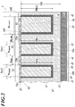
- FIG. 2 shows part of a section taken along line A-A in FIG. 1 .
- FIG. 3 is a sectional view showing a modification of the Schottky barrier diode according to the embodiment of the present disclosure.
- a Schottky barrier diode 1 has a plate shape. A portion surrounding and along the edge of the plate surface of the Schottky barrier diode 1 is referred to as an outer perimeter portion. On a vertical section of the Schottky barrier diode 1, a position closer to the outer perimeter portion may be referred to as an outer perimeter side, and a position closer to the center of the plate surface may be referred to as a center side.
- FIG. 2 shows the outer perimeter portion of the Schottky barrier diode 1 and the vicinity.
- the Schottky barrier diode 1 corresponds to an example of a semiconductor device according to the present disclosure.
- the Schottky barrier diode 1 As shown in FIG. 2 , the Schottky barrier diode 1 according to this embodiment has a pressure-resistant area 53 located on the outer perimeter side and rectifier areas 51a, 51b, 51c located on the center side when compared with the pressure-resistant area 53.
- the rectifier areas 51a, 51b, 51c are covered with the second electrode 22 from the above, and each of them is sandwiched, from the sides, between the outer surfaces of two adjacent tranches among inner trenches 31a, 31b and a perimeter trench 33.
- a Schottky barrier is generated at the interface between the second electrode 22 and an N - -type semiconductor of an epitaxial layer 13.
- the pressure-resistant area 53 is an area from the perimeter trench 33 to the outer perimeter end of a semiconductor layer 11.
- the pressure-resistant area 53 relieves concentration of the biased electric field that is applied to the semiconductor layer 11 from the outer perimeter end of the second electrode 22, and improves pressure resistance of the semiconductor layer 11.
- the Schottky barrier diode 1 includes the semiconductor layer 11, the first electrode 21 and the second electrode 22.
- the semiconductor layer 11 includes a semiconductor substrate 12 and the epitaxial layer 13.
- the semiconductor substrate 12 corresponds to an example of a first layer according to the present disclosure.
- the epitaxial layer 13 corresponds to an example of a second layer according to the present disclosure.
- the semiconductor substrate 12 is a silicon substrate, and is an N-type semiconductor containing a minute amount of impurities (that corresponds to an example of a first semiconductor of a first conductivity type according to the present disclosure).
- the impurities may be any of arsenic (As), phosphorus (P) and antimony (Sb).
- the semiconductor substrate 12 may be a P-type semiconductor.
- the N-type semiconductor in the following description may be replaced by the P-type semiconductor.
- the impurities may be boron (B) or aluminum (Al).
- the semiconductor substrate 12 may be a substrate including any of various semiconductors, such as silicon carbide (SiC), gallium nitride (GaN) and gallium oxide (Ga 2 O 3 ).
- silicon carbide (SiC) gallium nitride (GaN) and gallium oxide (Ga 2 O 3 ).
- an N-type semiconductor of silicon (Si) is used as the semiconductor substrate 12.
- a semiconductor having a high impurity concentration may be expressed by using "+" (plus), whereas a semiconductor having a low impurity concentration may be expressed by using "-" (minus).
- the semiconductor substrate 12 includes an N + -type semiconductor.
- the epitaxial layer 13 may be formed by using any of various known techniques, such as vapor deposition, molecular-beam epitaxy, sublimation, pyrolysis, CVD (Chemical Vapor Deposition) and mist CVD (Chemical Vapor Deposition).
- the epitaxial layer 13 is the same as the semiconductor substrate 12 in the conductivity type and contains the impurities at a lower concentration than the semiconductor substrate 12. That is, the epitaxial layer 13 includes an N - -type semiconductor (that corresponds to an example of a second semiconductor according to the present disclosure).
- the impurities contained in the semiconductor substrate 12 and the impurities contained in the epitaxial layer 13 may be different from one another.
- the epitaxial layer 13 has a plurality of inner trenches 31a, 31b and one perimeter trench 33.
- One of the inner trenches, 31a corresponds to an example of a first trench according to the present disclosure.
- the perimeter trench 33 corresponds to an example of a second trench according to the present disclosure.
- the other inner trench 31b corresponds to an example of a third trench according to the present disclosure.
- a plurality of inner trenches including the two inner trenches 31a, 31b may be disposed, in a plan view of the semiconductor layer 11, so as to be striped, or so as to surround the center side of the semiconductor layer 11.
- the number of inner trenches 31a, 31b may be three or more, or may be one by the inner trench 31b being omitted.
- the inner trenches 31a, 31b extend, in FIG. 2 and FIG. 3 , in the front-back direction on the plane of paper.
- the perimeter trench 33 is located in the pressure-resistant area 53 so as to surround the rectifier areas 51a, 51b, 51c. In other words, the perimeter trench 33 extends along the outer perimeter portion of the semiconductor layer 11 so as to cover the entire perimeter of the semiconductor layer 11.
- the perimeter trench 33 extends, in FIG. 2 and FIG. 3 , in the front-back direction on the place of paper, similarly to the inner trenches 31a, 31b.
- the first electrode 21 is in contact with a surface of the semiconductor substrate 12 opposite the epitaxial layer 13. This surface may be referred to as a first surface S1.
- the first surface S1 is located, in FIG. 2 , on the lower side on the plane of paper.
- the first electrode 21 contains a metal.
- the metal may be any of various metals including alloys.
- the first electrode 21 may be another conductor.
- the second electrode 22 is in contact with a surface of the epitaxial layer 13 opposite the semiconductor substrate 12. This surface may be referred to as a second surface S2.
- the second surface S2 is located, in FIG. 2 , on the upper side on the plane of paper.
- the second electrode 22 contains a metal.
- the metal may be any of various metals including alloys.
- the second electrode 22 may be another conductor.
- the inner trenches 31a, 31b and the perimeter trench 33 extend in the up-down direction (i.e. thickness direction) of the epitaxial layer 13.
- the inner trenches 31a, 31b and the perimeter trench 33 have therein inner field electrodes 23, 25, 24, respectively, extending in the thickness direction of the epitaxial layer 13.
- the inner field electrode 23 in the inner trench 31a may be referred to as a third electrode.
- the inner field electrode 24 in the perimeter trench 33 may be referred to as a fourth electrode.
- the inner field electrode 25 in the inner trench 31b may be referred to as a fifth electrode.
- the inner field electrodes 23 to 25 may be polysilicon.
- the inner field electrodes 23 to 25 may be other conductors. One surface of each of the inner field electrodes 23 to 25 is exposed at the second surface S2.
- the inner trenches 31a, 31b and the perimeter trench 33 further have insulating films 41 to 43, respectively, interposed between the inner field electrodes 23 to 25 and the N - -type semiconductor of the epitaxial layer 13.
- the insulating film 41 that the inner trench 31a has may be referred to as a first insulating film.
- the insulating film 42 that the perimeter trench 33 has may be referred to as a second insulating film.
- the insulating film 43 that the inner trench 31b has may be referred to as a third insulating film.
- the insulating films 41 to 43 may contain dielectrics.
- the inner field electrodes 23, 25 in the inner trenches 31a, 31b are capacitively coupled to the N - -type semiconductor of the epitaxial layer 13 via the insulating films 41, 43, respectively.
- the inner field electrode 24 in the perimeter trench 33 is capacitively coupled to the N - -type semiconductor of the epitaxial layer 13 via the insulating film 42.
- the entire outer perimeter end 22E of the second electrode 22 is located on the exposed surface of the inner field electrode 24 in the perimeter trench 33.
- the end (22E) of the second electrode 22 on the outer perimeter side is located in an area from an end 24E on the outer perimeter side to an end 241 on the center side of the inner field electrode 24.
- the inner field electrode 24 and the insulating film 42 may protrude from the second surface S2.
- the inner field electrode 24 and the insulating film 42 may run on the outside of the perimeter trench 33 to extend toward the outer perimeter side of the Schottky barrier diode 1.
- the outer perimeter end 22E of the second electrode 22 may extend to be on the protruding portion of the inner field electrode 24.
- the portion that runs on the outside of the perimeter trench 33 may be formed simultaneously with the insulating film 42 inside the perimeter trench 33.
- the second electrode 22 electrically connects with the inner field electrodes 23, 25 in the inner trenches 31a, 31b.
- the inner field electrodes 23, 25 form an electric field relief region in an area of the N - -type semiconductor sandwiched between the paired inner trenches 31a, 31b.
- the second electrode 22 also electrically connects with the inner field electrode 24 in the perimeter trench 33.
- This electrical connection produces the field plate effect and relieves concentration of the biased electric field on the outer perimeter portion of the semiconductor layer 11.
- the inner field electrode 24 in the perimeter trench 33 extends in the thickness direction of the epitaxial layer 13. Hence, the field plate effect by the perimeter trench 33 acts in the thickness direction of the epitaxial layer 13, and the peak of the electric field moves toward the bottom of the perimeter trench 33 when compared with a case where the inner field electrode 24 is not provided.
- the end of the inner field electrode 24 in the perimeter trench 33 on the pressure-resistant side is located at a point more forward than the end of the second electrode 22 in a direction from the rectifier areas 51a, 51b, 51c toward the pressure-resistant area 53.
- the peak of the electric field moves in the direction from the rectifier areas 51a, 51b, 51c toward the pressure-resistant area 53. Movement of the peak position of the electric field relieves concentration of the electric field, and hence even when the width of the pressure-resistant area 53 is made small, desired pressure resistance performance can be obtained.
- the area (size) of the rectifier areas 51a to 51c cannot be made small in terms of maintaining forward characteristics (forward voltage VF, etc.) of the Schottky barrier diode 1 at a predetermined value(s).
- the width of the pressure-resistant area 53 can be made small, and hence the chip size of the Schottky barrier diode 1 can be reduced by the amount.
- one surface of each of the inner field electrodes 23, 24 exposed at the second surface S2 may be substantially flush with the second surface S2 of the N - -type semiconductor of the epitaxial layer 13.
- One surface of each of the insulating films 41, 42 exposed at the second surface S2 may be substantially flush with the second surface S2 of the N - -type semiconductor of the epitaxial layer 13.
- at least an area E1 from the end of the inner trench 31a on the center side to the end of the inner field electrode 24 on the outer perimeter side is flat.
- an area E2 that contains all (both) the inner trenches 31a, 31b may be flat.
- a situation does not occur where part thereof protrudes upward or a step is generated. This improves step coverage in forming the second electrode 22 in the area E1 or E2.
- a resist in order for an electrode to be formed from the inner surface to the bottom of a perimeter trench, a resist needs to be molded into a predetermined shape at the bottom of the perimeter trench.
- molding accuracy of the resist decreases at the bottom.
- the first pass yield of Schottky barrier diodes decreases.
- processing accuracy of the second electrode 22 does not decrease, and hence the first pass yield can be improved.
- the depth TRE D of the inner trench 31a/31b and the depth TRE D 2 of the perimeter trench 33 may be substantially the same.
- the difference between the depth TRE D of the inner trench 31a/31b and the depth TRE D 2 of the perimeter trench 33 may be less than 10% of the depth TRE D of the inner trench 31a/31b.
- the depth direction is the thickness direction of the epitaxial layer 13.
- the depth TRE D of the inner trench 31a/31b is a direct distance from the second surface S2 of the epitaxial layer 13 to the point closest to the semiconductor substrate 12 on the bottom of the inner trench 31a/31b.
- the depth TRE D 2 of the perimeter trench 33 is a direct distance from the second surface S2 of the epitaxial layer 13 to the point closest to the semiconductor substrate 12 on the bottom of the perimeter trench 33.
- the depth TRE D of the perimeter trench 33 being substantially the same as the depth TRE D 2 of the inner trench 31a/31b allows the perimeter trench 33 to be also formed in a step in which the inner trenches 31a, 31b are formed.
- the number of steps increases because steps in which these are formed are separate, for example.
- the inner trenches 31a, 31b and the perimeter trench 33 can be formed in the same step.
- the depth of the inner trench 31a/31b and the depth of the perimeter trench 33 may be different by 10% or more.
- the perimeter trench 33 being deeper than the inner trench 31a/31b can improve pressure resistance performance of the Schottky barrier diode 1A against the reverse voltage.
- E pit represents the thickness of the epitaxial layer 13
- TRE D represents the depth of the inner trench 31a/31b
- a relationship between E pit and TRE D may be 0.30 ⁇ E pit ⁇ TRE D ⁇ 0.80 ⁇ E pit . With this relationship, the Schottky barrier diode 1 obtains desired pressure resistance.
- E pit represents the thickness of the epitaxial layer 13
- TRE D 2 represents the depth of the perimeter trench 33
- a relationship between E pit and TRE D 2 may be 0.30 ⁇ E pit ⁇ TRE D 2 ⁇ 0.80 ⁇ E pit .
- TRE D TRE D 2. With this relationship, the Schottky barrier diode 1 obtains desired pressure resistance.
- the two inner trenches 31a, 31b are referred to as a first inner trench 31a and a second inner trench 31b.
- the second inner trench 31b is located next to the first inner trench 31a and opposite the perimeter trench 33 across it. That is, from the center side to the outer perimeter side of the second surface S2, the second inner trench 31b, the first inner trench 31a and the perimeter trench 33 line up in this order.
- the second inner trench 31b extends parallel to the first inner trench 31a.
- the insulating film 41 in the first inner trench 31a and the insulating film 43 in the second inner trench 31b may have the same thickness.
- W SDB represents the distance between the first inner trench 31a and the second inner trench 31b
- T OXI 1 represents the thickness of the insulating film 41
- W SBD /T OXI 1 ⁇ 5.5 may hold.
- the W SBD may be referred to as the width of the N - -type semiconductor between the first inner trench 31a and the second inner trench 31b.
- T OXI 3 represents the thickness of the insulating film 43
- W SBD /T OXI 3 ⁇ 5.5 may hold.
- the perimeter trench 33 and the first inner trench 31a extend parallel to one another.
- W E-SBD represents the distance between the perimeter trench 33 and the inner trench 31a
- W E-SBD ⁇ W SBD may hold.
- the W E-SBD may be referred to as the width of the N - -type semiconductor between the perimeter trench 33 and the inner trench 31a. With this relationship, the Schottky barrier diode 1 obtains desired pressure resistance.
- W trench 1 represents the width of the first inner trench 31a
- W E-trench represents the width of the perimeter trench 33
- W trench 1 ⁇ W E-trench may hold.
- W trench 2 represents the width of the second inner trench 31b
- W E-trench represents the width of the perimeter trench 33
- W trench 2 ⁇ W E-trench may hold.
- each of various trenches contains an inner field electrode and an insulating film. That is, the depth thereof is a direct distance from the second surface S2 to the point closest to the semiconductor substrate 12 on the insulating film in the trench, and the width thereof is determined on the basis of the outer edge of the insulating film.
- the perimeter trench is shown as the outermost trench, but another trench may be disposed closer to the outer perimeter side of the semiconductor layer than the perimeter trench.
- the Schottky barrier diode 1 is described as an example.
- the semiconductor device according to the present disclosure may be a diode, a transistor or the like having a trench structure at the outer perimeter portion of a semiconductor layer.
- the Schottky barrier diode 1 of the embodiment or the semiconductor device according to the present disclosure may be provided to various electric devices. Examples of the electric devices include a power module having a power supply circuit that performs power conversion. Examples of the electric devices also include various electronic devices, trains and automobiles.
- the present invention is applicable to a semiconductor device and an electric device.
Landscapes
- Electrodes Of Semiconductors (AREA)
Abstract
Description
- The present disclosure relates to a semiconductor device and an electric device.
- There is disclosed in Patent Literature 1, as a semiconductor device, a trenched Schottky rectifier in which a plurality of trenches is formed in a semiconductor layer. These trenches include a perimeter trench disposed close to the outer perimeter portion of the semiconductor layer and an inner trench disposed far from the outer perimeter portion of the semiconductor layer when compared with the perimeter trench.
- Patent Literature 1:
JP 2003-522513 A - A semiconductor device of the present disclosure includes:
- a first layer having a first semiconductor containing an impurity of a first conductivity type;
- a second layer being in contact with the first layer and having a second semiconductor containing the impurity of the first conductivity type at a lower concentration than the first semiconductor;
- a first electrode being in contact with a first surface of the first layer opposite the second layer; and
- a second electrode being in contact with a second surface of the second layer opposite the first layer,
- wherein the second layer further has:
- a first trench having therein a third electrode connected to the second electrode; and
- a second trench located closer to an outer perimeter portion of the second layer than the first trench and having therein a fourth electrode connected to the second electrode, and
- wherein an entire outer perimeter end of the second electrode that is in contact with the second surface between the first trench and the second trench is in contact with the fourth electrode.
- An electric device of the present disclosure includes a semiconductor device including:
- a first layer having a first semiconductor containing an impurity of a first conductivity type;
- a second layer being in contact with the first layer and having a second semiconductor containing the impurity of the first conductivity type at a lower concentration than the first semiconductor;
- a first electrode being in contact with a first surface of the first layer opposite the second layer; and
- a second electrode being in contact with a second surface of the second layer opposite the first layer,
- wherein the second layer further has:
- a first trench having therein a third electrode connected to the second electrode; and
- a second trench located closer to an outer perimeter portion of the second layer than the first trench and having therein a fourth electrode connected to the second electrode, and
- wherein an entire outer perimeter end of the second electrode that is in contact with the second surface between the first trench and the second trench is in contact with the fourth electrode.
-
-
FIG. 1 is a perspective view showing a Schottky barrier diode according to an embodiment of the present disclosure. -
FIG. 2 shows part of a section taken along line A-A inFIG. 1 . -
FIG. 3 is a sectional view showing a modification of the Schottky barrier diode according to the embodiment of the present disclosure. - Hereinafter, an embodiment of the present disclosure will be described in detail with reference to the drawings. However, detailed descriptions of well-known matters, duplicate matters and the like may be omitted. The drawings and the following description are for those skilled in the art to fully understand the present disclosure. Hence, the drawings and the following description are not intended to limit the subject matters set forth in the scope of claims. All the drawings are diagrammatic. Relative dimensions of parts in the drawings may be changed to be larger or smaller as appropriate.
-
FIG. 1 is a perspective view showing a Schottky barrier diode according to an embodiment of the present disclosure.FIG. 2 shows part of a section taken along line A-A inFIG. 1 .FIG. 3 is a sectional view showing a modification of the Schottky barrier diode according to the embodiment of the present disclosure. - In this embodiment, a direction from a
first electrode 21 toward asecond electrode 22 may be referred to as upward or an up direction, and the opposite direction may be referred to as downward or a down direction. A Schottky barrier diode 1 according to this embodiment has a plate shape. A portion surrounding and along the edge of the plate surface of the Schottky barrier diode 1 is referred to as an outer perimeter portion. On a vertical section of the Schottky barrier diode 1, a position closer to the outer perimeter portion may be referred to as an outer perimeter side, and a position closer to the center of the plate surface may be referred to as a center side.FIG. 2 shows the outer perimeter portion of the Schottky barrier diode 1 and the vicinity. The Schottky barrier diode 1 corresponds to an example of a semiconductor device according to the present disclosure. - As shown in
FIG. 2 , the Schottky barrier diode 1 according to this embodiment has a pressure-resistant area 53 located on the outer perimeter side andrectifier areas resistant area 53. - The
rectifier areas second electrode 22 from the above, and each of them is sandwiched, from the sides, between the outer surfaces of two adjacent tranches amonginner trenches perimeter trench 33. In therectifier areas second electrode 22 and an N--type semiconductor of anepitaxial layer 13. - The pressure-
resistant area 53 is an area from theperimeter trench 33 to the outer perimeter end of asemiconductor layer 11. When the reverse voltage is applied to the Schottky barrier electrode 1, the pressure-resistant area 53 relieves concentration of the biased electric field that is applied to thesemiconductor layer 11 from the outer perimeter end of thesecond electrode 22, and improves pressure resistance of thesemiconductor layer 11. - The Schottky barrier diode 1 includes the
semiconductor layer 11, thefirst electrode 21 and thesecond electrode 22. Thesemiconductor layer 11 includes asemiconductor substrate 12 and theepitaxial layer 13. Thesemiconductor substrate 12 corresponds to an example of a first layer according to the present disclosure. Theepitaxial layer 13 corresponds to an example of a second layer according to the present disclosure. - The
semiconductor substrate 12 is a silicon substrate, and is an N-type semiconductor containing a minute amount of impurities (that corresponds to an example of a first semiconductor of a first conductivity type according to the present disclosure). The impurities may be any of arsenic (As), phosphorus (P) and antimony (Sb). Thesemiconductor substrate 12 may be a P-type semiconductor. When thesemiconductor substrate 12 is a P-type semiconductor, the N-type semiconductor in the following description may be replaced by the P-type semiconductor. When thesemiconductor substrate 12 is the P-type, the impurities may be boron (B) or aluminum (Al). Thesemiconductor substrate 12 may be a substrate including any of various semiconductors, such as silicon carbide (SiC), gallium nitride (GaN) and gallium oxide (Ga2O3). In this embodiment, as an example, an N-type semiconductor of silicon (Si) is used as thesemiconductor substrate 12. A semiconductor having a high impurity concentration may be expressed by using "+" (plus), whereas a semiconductor having a low impurity concentration may be expressed by using "-" (minus). Thesemiconductor substrate 12 includes an N+-type semiconductor. - The
epitaxial layer 13 may be formed by using any of various known techniques, such as vapor deposition, molecular-beam epitaxy, sublimation, pyrolysis, CVD (Chemical Vapor Deposition) and mist CVD (Chemical Vapor Deposition). Theepitaxial layer 13 is the same as thesemiconductor substrate 12 in the conductivity type and contains the impurities at a lower concentration than thesemiconductor substrate 12. That is, theepitaxial layer 13 includes an N--type semiconductor (that corresponds to an example of a second semiconductor according to the present disclosure). The impurities contained in thesemiconductor substrate 12 and the impurities contained in theepitaxial layer 13 may be different from one another. - The
epitaxial layer 13 has a plurality ofinner trenches perimeter trench 33. One of the inner trenches, 31a, corresponds to an example of a first trench according to the present disclosure. Theperimeter trench 33 corresponds to an example of a second trench according to the present disclosure. The otherinner trench 31b corresponds to an example of a third trench according to the present disclosure. - A plurality of inner trenches including the two
inner trenches semiconductor layer 11, so as to be striped, or so as to surround the center side of thesemiconductor layer 11. The number ofinner trenches inner trench 31b being omitted. Theinner trenches FIG. 2 andFIG. 3 , in the front-back direction on the plane of paper. - The
perimeter trench 33 is located in the pressure-resistant area 53 so as to surround therectifier areas perimeter trench 33 extends along the outer perimeter portion of thesemiconductor layer 11 so as to cover the entire perimeter of thesemiconductor layer 11. Theperimeter trench 33 extends, inFIG. 2 andFIG. 3 , in the front-back direction on the place of paper, similarly to theinner trenches - The
first electrode 21 is in contact with a surface of thesemiconductor substrate 12 opposite theepitaxial layer 13. This surface may be referred to as a first surface S1. The first surface S1 is located, inFIG. 2 , on the lower side on the plane of paper. Thefirst electrode 21 contains a metal. The metal may be any of various metals including alloys. Thefirst electrode 21 may be another conductor. - The
second electrode 22 is in contact with a surface of theepitaxial layer 13 opposite thesemiconductor substrate 12. This surface may be referred to as a second surface S2. The second surface S2 is located, inFIG. 2 , on the upper side on the plane of paper. Thesecond electrode 22 contains a metal. The metal may be any of various metals including alloys. Thesecond electrode 22 may be another conductor. - The
inner trenches perimeter trench 33 extend in the up-down direction (i.e. thickness direction) of theepitaxial layer 13. Theinner trenches perimeter trench 33 have thereininner field electrodes epitaxial layer 13. Theinner field electrode 23 in theinner trench 31a may be referred to as a third electrode. Theinner field electrode 24 in theperimeter trench 33 may be referred to as a fourth electrode. Theinner field electrode 25 in theinner trench 31b may be referred to as a fifth electrode. Theinner field electrodes 23 to 25 may be polysilicon. Theinner field electrodes 23 to 25 may be other conductors. One surface of each of theinner field electrodes 23 to 25 is exposed at the second surface S2. - The
inner trenches perimeter trench 33 further have insulatingfilms 41 to 43, respectively, interposed between theinner field electrodes 23 to 25 and the N--type semiconductor of theepitaxial layer 13. The insulatingfilm 41 that theinner trench 31a has may be referred to as a first insulating film. The insulatingfilm 42 that theperimeter trench 33 has may be referred to as a second insulating film. The insulatingfilm 43 that theinner trench 31b has may be referred to as a third insulating film. The insulatingfilms 41 to 43 may contain dielectrics. Theinner field electrodes inner trenches epitaxial layer 13 via the insulatingfilms inner field electrode 24 in theperimeter trench 33 is capacitively coupled to the N--type semiconductor of theepitaxial layer 13 via the insulatingfilm 42. - The entire
outer perimeter end 22E of thesecond electrode 22 is located on the exposed surface of theinner field electrode 24 in theperimeter trench 33. In other words, on the entire perimeter of the Schottky barrier diode 1, when viewed from the above, the end (22E) of thesecond electrode 22 on the outer perimeter side is located in an area from anend 24E on the outer perimeter side to anend 241 on the center side of theinner field electrode 24. - The
inner field electrode 24 and the insulatingfilm 42 may protrude from the second surface S2. Theinner field electrode 24 and the insulatingfilm 42 may run on the outside of theperimeter trench 33 to extend toward the outer perimeter side of the Schottky barrier diode 1. When theinner field electrode 24 and the insulatingfilm 42 extend outside theperimeter trench 33, theouter perimeter end 22E of thesecond electrode 22 may extend to be on the protruding portion of theinner field electrode 24. Of the insulatingfilm 42, the portion that runs on the outside of theperimeter trench 33 may be formed simultaneously with the insulatingfilm 42 inside theperimeter trench 33. - The
second electrode 22 electrically connects with theinner field electrodes inner trenches inner field electrodes inner trenches first electrode 21 and thesecond electrode 22 in the blocking state of the Schottky barrier diode 1, the Schottky barrier in therectifier areas - The
second electrode 22 also electrically connects with theinner field electrode 24 in theperimeter trench 33. This electrical connection produces the field plate effect and relieves concentration of the biased electric field on the outer perimeter portion of thesemiconductor layer 11. Theinner field electrode 24 in theperimeter trench 33 extends in the thickness direction of theepitaxial layer 13. Hence, the field plate effect by theperimeter trench 33 acts in the thickness direction of theepitaxial layer 13, and the peak of the electric field moves toward the bottom of theperimeter trench 33 when compared with a case where theinner field electrode 24 is not provided. The end of theinner field electrode 24 in theperimeter trench 33 on the pressure-resistant side is located at a point more forward than the end of thesecond electrode 22 in a direction from therectifier areas resistant area 53. Hence, the peak of the electric field moves in the direction from therectifier areas resistant area 53. Movement of the peak position of the electric field relieves concentration of the electric field, and hence even when the width of the pressure-resistant area 53 is made small, desired pressure resistance performance can be obtained. - The area (size) of the
rectifier areas 51a to 51c cannot be made small in terms of maintaining forward characteristics (forward voltage VF, etc.) of the Schottky barrier diode 1 at a predetermined value(s). However, the width of the pressure-resistant area 53 can be made small, and hence the chip size of the Schottky barrier diode 1 can be reduced by the amount. - In this embodiment, one surface of each of the
inner field electrodes epitaxial layer 13. One surface of each of the insulatingfilms epitaxial layer 13. In other words, of the second surface S2, at least an area E1 from the end of theinner trench 31a on the center side to the end of theinner field electrode 24 on the outer perimeter side is flat. Of the second surface S2, an area E2 that contains all (both) theinner trenches second electrode 22 in the area E1 or E2. - For example, in order for an electrode to be formed from the inner surface to the bottom of a perimeter trench, a resist needs to be molded into a predetermined shape at the bottom of the perimeter trench. However, molding accuracy of the resist decreases at the bottom. Hence, the first pass yield of Schottky barrier diodes decreases. In this embodiment, processing accuracy of the
second electrode 22 does not decrease, and hence the first pass yield can be improved. - The depth TRED of the
inner trench 31a/31b and thedepth TRE D2 of theperimeter trench 33 may be substantially the same. For example, the difference between the depth TRED of theinner trench 31a/31b and thedepth TRE D2 of theperimeter trench 33 may be less than 10% of the depth TRED of theinner trench 31a/31b. The depth direction is the thickness direction of theepitaxial layer 13. The depth TRED of theinner trench 31a/31b is a direct distance from the second surface S2 of theepitaxial layer 13 to the point closest to thesemiconductor substrate 12 on the bottom of theinner trench 31a/31b. Similarly, thedepth TRE D2 of theperimeter trench 33 is a direct distance from the second surface S2 of theepitaxial layer 13 to the point closest to thesemiconductor substrate 12 on the bottom of theperimeter trench 33. The depth TRED of theperimeter trench 33 being substantially the same as thedepth TRE D2 of theinner trench 31a/31b allows theperimeter trench 33 to be also formed in a step in which theinner trenches - For example, when the depth of a perimeter trench is different from the depth of an inner trench by 10% or more, the number of steps increases because steps in which these are formed are separate, for example. In this embodiment, the
inner trenches perimeter trench 33 can be formed in the same step. - As in a
Schottky barrier diode 1A of a modification shown inFIG. 3 , the depth of theinner trench 31a/31b and the depth of theperimeter trench 33 may be different by 10% or more. Theperimeter trench 33 being deeper than theinner trench 31a/31b can improve pressure resistance performance of theSchottky barrier diode 1A against the reverse voltage. - When Epit represents the thickness of the
epitaxial layer 13, and TRED represents the depth of theinner trench 31a/31b, a relationship between Epit and TRED may be 0.30 × Epit ≤ TRED ≤ 0.80 × Epit. With this relationship, the Schottky barrier diode 1 obtains desired pressure resistance. - When Epit represents the thickness of the
epitaxial layer 13, andTRE D2 represents the depth of theperimeter trench 33, a relationship between Epit andTRE D2 may be 0.30 × Epit ≤TRE D2 ≤ 0.80 × Epit. When the depth of theinner trench 31a/31b and the depth of theperimeter trench 33 are the same, TRED =TRE D2. With this relationship, the Schottky barrier diode 1 obtains desired pressure resistance. - For the sake of easy explanation, the two
inner trenches inner trench 31a and a secondinner trench 31b. The secondinner trench 31b is located next to the firstinner trench 31a and opposite theperimeter trench 33 across it. That is, from the center side to the outer perimeter side of the second surface S2, the secondinner trench 31b, the firstinner trench 31a and theperimeter trench 33 line up in this order. The secondinner trench 31b extends parallel to the firstinner trench 31a. The insulatingfilm 41 in the firstinner trench 31a and the insulatingfilm 43 in the secondinner trench 31b may have the same thickness. When WSDB represents the distance between the firstinner trench 31a and the secondinner trench 31b, and TOXI1 represents the thickness of the insulatingfilm 41, WSBD/TOXI1 ≤ 5.5 may hold. The WSBD may be referred to as the width of the N--type semiconductor between the firstinner trench 31a and the secondinner trench 31b. When TOXI3 represents the thickness of the insulatingfilm 43, WSBD/TOXI3 ≤ 5.5 may hold. With these relationships, the Schottky barrier diode 1 obtains desired pressure resistance. - The
perimeter trench 33 and the firstinner trench 31a extend parallel to one another. When WE-SBD represents the distance between theperimeter trench 33 and theinner trench 31a, WE-SBD ≤ WSBD may hold. The WE-SBD may be referred to as the width of the N--type semiconductor between theperimeter trench 33 and theinner trench 31a. With this relationship, the Schottky barrier diode 1 obtains desired pressure resistance. - When Wtrench1 represents the width of the first
inner trench 31a, and WE-trench represents the width of theperimeter trench 33, Wtrench1 ≤ WE-trench may hold. WhenW trench2 represents the width of the secondinner trench 31b, and WE-trench represents the width of theperimeter trench 33,W trench2 ≤ WE-trench may hold. With this relationship, the Schottky barrier diode 1 obtains desired pressure resistance. - In the embodiment, dimensions, such as the depth and the width, of each of various trenches are shown. The trenches shown herein each contain an inner field electrode and an insulating film. That is, the depth thereof is a direct distance from the second surface S2 to the point closest to the
semiconductor substrate 12 on the insulating film in the trench, and the width thereof is determined on the basis of the outer edge of the insulating film. In the drawings, the perimeter trench is shown as the outermost trench, but another trench may be disposed closer to the outer perimeter side of the semiconductor layer than the perimeter trench. - In the embodiment, as the semiconductor device according to the present disclosure, the Schottky barrier diode 1 is described as an example. However, the semiconductor device according to the present disclosure may be a diode, a transistor or the like having a trench structure at the outer perimeter portion of a semiconductor layer. The Schottky barrier diode 1 of the embodiment or the semiconductor device according to the present disclosure may be provided to various electric devices. Examples of the electric devices include a power module having a power supply circuit that performs power conversion. Examples of the electric devices also include various electronic devices, trains and automobiles.
- The description of the embodiment is illustrative in every aspect, and hence the present invention is not limited thereto. The present disclosure is applicable to the embodiment subjected to appropriate combination, change, replacement, addition, omission and/or the like of the aspect(s) as far as there is no inconsistency. It is appreciated that not-shown numerous modifications can be envisaged without departing from the scope of the present invention.
- The present invention is applicable to a semiconductor device and an electric device.
-
- 1
- Schottky Barrier Diode (Semiconductor Device)
- 11
- Semiconductor Layer
- 12
- Semiconductor Substrate
- 13
- Epitaxial Layer
- 21
- First Electrode
- 22
- Second Electrode
- 22E
- Outer Perimeter End of Second Electrode
- 31a
- Inner Trench (First Trench)
- 31b
- Inner Trench (Third Trench)
- 33
- Perimeter Trench (Second Trench)
- 51a, 51b, 51c
- Rectifier Area
- 53
- Pressure-resistant Area
- S1
- First Surface
- S2
- Second Surface
- 23
- Inner Field Electrode (Third Electrode)
- 24
- Inner Field Electrode (Fourth Electrode)
- 25
- Inner Field Electrode (Fifth Electrode)
- 41
- Insulating Film (First Insulating Film)
- 42
- Insulating Film (Second Insulating Film)
- 43
- Insulating Film (Third Insulating Film)
Claims (11)
- A semiconductor device comprising:a first layer having a first semiconductor containing an impurity of a first conductivity type;a second layer being in contact with the first layer and having a second semiconductor containing the impurity of the first conductivity type at a lower concentration than the first semiconductor;a first electrode being in contact with a first surface of the first layer opposite the second layer; anda second electrode being in contact with a second surface of the second layer opposite the first layer,wherein the second layer further has:a first trench having therein a third electrode connected to the second electrode; anda second trench located closer to an outer perimeter portion of the second layer than the first trench and having therein a fourth electrode connected to the second electrode, andwherein an entire outer perimeter end of the second electrode that is in contact with the second surface between the first trench and the second trench is in contact with the fourth electrode.
- The semiconductor device according to claim 1, wherein the first conductivity type is a P-type.
- The semiconductor device according to claim 1, wherein the first conductivity type is an N-type.
- The semiconductor device according to any one of claims 1 to 3, wherein a difference between a depth of the first trench and a depth of the second trench is less than 10% of the depth of the first trench.
- The semiconductor device according to claim 4, wherein a relationship between a thickness Epit of the second layer and the depth represented by TRED of the first trench or the second trench is 0.30 × Epit ≤ TRED ≤ 0.80 × Epit.
- The semiconductor device according to any one of claims 1 to 5,
wherein the second layer further has a third trench located farther from the outer perimeter portion of the second layer than the first trench and having therein a fifth electrode connected to the second electrode,
wherein the first trench further has therein a first insulating film interposed between the second semiconductor and the third electrode,
wherein the second trench further has therein a second insulating film interposed between the second semiconductor and the fourth electrode,
wherein the third trench further has therein a third insulating film interposed between the second semiconductor and the fifth electrode,
wherein a relationship between a thickness TOXI1 of the first insulating film and a width WSBD of the second semiconductor interposed between the first trench and the third trench is WSBD/TOXI1 ≤ 5.5, and
wherein a relationship between a thickness TOXI3 of the third insulating film and the width WSBD is WSBD/TOXI3 ≤ 5.5. - The semiconductor device according to claim 6, wherein a relationship between a width WE-SBD of the second semiconductor interposed between the first trench and the second trench and the width WSBD is WE-SBD ≤ WSBD.
- The semiconductor device according to claim 7,
wherein a relationship between a width Wtrench1 of the first trench and a width WE-trench of the second trench is Wtrench1 ≤ WE-trench, and
wherein a relationship between a width Wtrench3 of the third trench and the width WE-trench of the second trench is Wtrench3 ≤ WE-trench. - The semiconductor device according to any one of claims 1 to 8, wherein the second surface is flat at least from an end of the first trench on a side far from the second trench to an end of the fourth electrode on a side close to the outer perimeter portion of the second layer.
- An electric device comprising a semiconductor device comprising:a first layer having a first semiconductor containing an impurity of a first conductivity type;a second layer being in contact with the first layer and having a second semiconductor containing the impurity of the first conductivity type at a lower concentration than the first semiconductor;a first electrode being in contact with a first surface of the first layer opposite the second layer; anda second electrode being in contact with a second surface of the second layer opposite the first layer,wherein the second layer further has:a first trench having therein a third electrode connected to the second electrode; anda second trench located closer to an outer perimeter portion of the second layer than the first trench and having therein a fourth electrode connected to the second electrode, andwherein an entire outer perimeter end of the second electrode that is in contact with the second surface between the first trench and the second trench is in contact with the fourth electrode.
- The semiconductor device according to any one of claims 1 to 3, wherein the second trench is deeper than the first trench.
Applications Claiming Priority (2)
| Application Number | Priority Date | Filing Date | Title |
|---|---|---|---|
| JP2018124659A JP6626929B1 (en) | 2018-06-29 | 2018-06-29 | Semiconductor devices and electrical equipment |
| PCT/JP2019/025296 WO2020004437A1 (en) | 2018-06-29 | 2019-06-26 | Semiconductor device and electric device |
Publications (2)
| Publication Number | Publication Date |
|---|---|
| EP3817069A1 true EP3817069A1 (en) | 2021-05-05 |
| EP3817069A4 EP3817069A4 (en) | 2022-03-16 |
Family
ID=68986305
Family Applications (1)
| Application Number | Title | Priority Date | Filing Date |
|---|---|---|---|
| EP19826828.6A Pending EP3817069A4 (en) | 2018-06-29 | 2019-06-26 | SEMICONDUCTOR DEVICE AND ELECTRICAL DEVICE |
Country Status (6)
| Country | Link |
|---|---|
| US (1) | US11393933B2 (en) |
| EP (1) | EP3817069A4 (en) |
| JP (1) | JP6626929B1 (en) |
| KR (1) | KR20210011445A (en) |
| CN (1) | CN112352319B (en) |
| WO (1) | WO2020004437A1 (en) |
Families Citing this family (8)
| Publication number | Priority date | Publication date | Assignee | Title |
|---|---|---|---|---|
| JP7304827B2 (en) * | 2020-01-20 | 2023-07-07 | 三菱電機株式会社 | Semiconductor device and crack detection method |
| JP7684816B2 (en) * | 2021-02-25 | 2025-05-28 | Tdk株式会社 | Schottky Barrier Diode |
| JP7669159B2 (en) * | 2021-02-25 | 2025-04-28 | Tdk株式会社 | Schottky Barrier Diode |
| US20240191391A1 (en) * | 2021-04-16 | 2024-06-13 | Kyocera Corporation | SEMICONDUCTOR SUBSTRATE, MANUFACTURING METHOD AND MANUFACTURING APPARATUS THEREFOR, GaN-BASED CRYSTAL BODY, SEMICONDUCTOR DEVICE, AND ELECTRONIC DEVICE |
| TW202306179A (en) * | 2021-06-07 | 2023-02-01 | 日商Flosfia股份有限公司 | Semiconductor device |
| TW202315140A (en) * | 2021-06-07 | 2023-04-01 | 日商Flosfia股份有限公司 | Semiconductor device |
| WO2023018769A1 (en) * | 2021-08-10 | 2023-02-16 | Ideal Power Inc. | System and method for bi-directional trench power switches |
| JP2024033852A (en) * | 2022-08-31 | 2024-03-13 | Tdk株式会社 | schottky barrier diode |
Family Cites Families (26)
| Publication number | Priority date | Publication date | Assignee | Title |
|---|---|---|---|---|
| GB0002235D0 (en) | 2000-02-02 | 2000-03-22 | Koninkl Philips Electronics Nv | Trenched schottky rectifiers |
| DE10005183A1 (en) | 2000-02-05 | 2001-08-09 | Bosch Gmbh Robert | Rectifier arrangement |
| KR20090116702A (en) * | 2007-01-09 | 2009-11-11 | 맥스파워 세미컨덕터 인크. | Semiconductor devices |
| US8022472B2 (en) * | 2007-12-04 | 2011-09-20 | Rohm Co., Ltd. | Semiconductor device and method of manufacturing semiconductor device |
| US8076719B2 (en) * | 2008-02-14 | 2011-12-13 | Maxpower Semiconductor, Inc. | Semiconductor device structures and related processes |
| JP4535151B2 (en) * | 2008-03-19 | 2010-09-01 | 株式会社デンソー | Method for manufacturing silicon carbide semiconductor device |
| JP4640439B2 (en) * | 2008-04-17 | 2011-03-02 | 株式会社デンソー | Silicon carbide semiconductor device |
| US7960781B2 (en) * | 2008-09-08 | 2011-06-14 | Semiconductor Components Industries, Llc | Semiconductor device having vertical charge-compensated structure and sub-surface connecting layer and method |
| CN101800252B (en) * | 2010-03-04 | 2012-05-30 | 无锡新洁能功率半导体有限公司 | Groove-shaped Schottky barrier rectifier and manufacture method thereof |
| JP5449094B2 (en) * | 2010-09-07 | 2014-03-19 | 株式会社東芝 | Semiconductor device |
| JP5671966B2 (en) * | 2010-11-17 | 2015-02-18 | 富士電機株式会社 | Semiconductor device manufacturing method and semiconductor device |
| JP6053103B2 (en) * | 2012-04-12 | 2016-12-27 | 富士電機株式会社 | Wide band gap semiconductor device and method of manufacturing the same |
| US9142668B2 (en) * | 2013-03-13 | 2015-09-22 | Cree, Inc. | Field effect transistor devices with buried well protection regions |
| JP6295444B2 (en) * | 2013-07-16 | 2018-03-20 | パナソニックIpマネジメント株式会社 | Semiconductor device |
| JP6296445B2 (en) * | 2014-02-10 | 2018-03-20 | ローム株式会社 | Schottky barrier diode |
| JP2016152357A (en) * | 2015-02-18 | 2016-08-22 | 株式会社東芝 | Semiconductor device and semiconductor package |
| JP6185504B2 (en) * | 2015-03-24 | 2017-08-23 | 京セラ株式会社 | Semiconductor device |
| JP6613610B2 (en) * | 2015-05-14 | 2019-12-04 | 富士電機株式会社 | Semiconductor device and manufacturing method of semiconductor device |
| JP6260605B2 (en) * | 2015-11-19 | 2018-01-17 | トヨタ自動車株式会社 | Semiconductor device |
| JP6378220B2 (en) * | 2016-02-01 | 2018-08-22 | 株式会社東芝 | Semiconductor device |
| JP6416143B2 (en) * | 2016-03-16 | 2018-10-31 | 株式会社東芝 | Semiconductor device |
| JP6845397B2 (en) * | 2016-04-28 | 2021-03-17 | 株式会社タムラ製作所 | Trench MOS type Schottky diode |
| US10304971B2 (en) * | 2016-07-16 | 2019-05-28 | Champion Microelectronic Corp. | High speed Schottky rectifier |
| JP6996082B2 (en) * | 2016-12-22 | 2022-01-17 | 富士電機株式会社 | Semiconductor devices and methods for manufacturing semiconductor devices |
| JP7020185B2 (en) * | 2017-03-15 | 2022-02-16 | 富士電機株式会社 | Semiconductor device |
| JP7305591B2 (en) * | 2020-03-24 | 2023-07-10 | 株式会社東芝 | semiconductor equipment |
-
2018
- 2018-06-29 JP JP2018124659A patent/JP6626929B1/en active Active
-
2019
- 2019-06-26 EP EP19826828.6A patent/EP3817069A4/en active Pending
- 2019-06-26 CN CN201980041794.7A patent/CN112352319B/en active Active
- 2019-06-26 KR KR1020207037002A patent/KR20210011445A/en not_active Ceased
- 2019-06-26 US US17/253,970 patent/US11393933B2/en active Active
- 2019-06-26 WO PCT/JP2019/025296 patent/WO2020004437A1/en not_active Ceased
Also Published As
| Publication number | Publication date |
|---|---|
| CN112352319A (en) | 2021-02-09 |
| CN112352319B (en) | 2023-10-10 |
| KR20210011445A (en) | 2021-02-01 |
| EP3817069A4 (en) | 2022-03-16 |
| JP2020004906A (en) | 2020-01-09 |
| WO2020004437A1 (en) | 2020-01-02 |
| JP6626929B1 (en) | 2019-12-25 |
| US20210265511A1 (en) | 2021-08-26 |
| US11393933B2 (en) | 2022-07-19 |
Similar Documents
| Publication | Publication Date | Title |
|---|---|---|
| US11393933B2 (en) | Semiconductor device and electric device | |
| US20240234529A1 (en) | Wide band gap semiconductor device with surface insulating film | |
| US12439655B2 (en) | Semiconductor device with voltage resistant structure | |
| US9041098B2 (en) | Semiconductor device | |
| JP6061181B2 (en) | Semiconductor device | |
| US8643091B2 (en) | Semiconductor device | |
| US8421148B2 (en) | Grid-UMOSFET with electric field shielding of gate oxide | |
| US9035355B2 (en) | Multi-channel HEMT | |
| US20200212219A1 (en) | Vertical trench gate mosfet with integrated schottky diode | |
| US10903351B2 (en) | Semiconductor device | |
| EP2502275A1 (en) | Lateral power transistor device and method of manufacturing the same | |
| US11769805B2 (en) | Semiconductor device with field plate electrode | |
| KR102387574B1 (en) | Power semiconductor device | |
| US11342435B2 (en) | Wide-gap semiconductor device | |
| US20250098234A1 (en) | Semiconductor device | |
| US20260090043A1 (en) | Semiconductor device | |
| US20240096972A1 (en) | Semiconductor device | |
| US20240021681A1 (en) | Semiconductor device | |
| US20250098284A1 (en) | Semiconductor device | |
| US20240313106A1 (en) | Semiconductor device | |
| US20250294831A1 (en) | Semiconductor device | |
| KR102417146B1 (en) | Power semiconductor device | |
| US20250311336A1 (en) | Semiconductor device |
Legal Events
| Date | Code | Title | Description |
|---|---|---|---|
| STAA | Information on the status of an ep patent application or granted ep patent |
Free format text: STATUS: THE INTERNATIONAL PUBLICATION HAS BEEN MADE |
|
| PUAI | Public reference made under article 153(3) epc to a published international application that has entered the european phase |
Free format text: ORIGINAL CODE: 0009012 |
|
| STAA | Information on the status of an ep patent application or granted ep patent |
Free format text: STATUS: REQUEST FOR EXAMINATION WAS MADE |
|
| 17P | Request for examination filed |
Effective date: 20201221 |
|
| AK | Designated contracting states |
Kind code of ref document: A1 Designated state(s): AL AT BE BG CH CY CZ DE DK EE ES FI FR GB GR HR HU IE IS IT LI LT LU LV MC MK MT NL NO PL PT RO RS SE SI SK SM TR |
|
| DAV | Request for validation of the european patent (deleted) | ||
| DAX | Request for extension of the european patent (deleted) | ||
| A4 | Supplementary search report drawn up and despatched |
Effective date: 20220216 |
|
| RIC1 | Information provided on ipc code assigned before grant |
Ipc: H01L 29/24 20060101ALN20220210BHEP Ipc: H01L 29/20 20060101ALN20220210BHEP Ipc: H01L 29/16 20060101ALN20220210BHEP Ipc: H01L 29/47 20060101ALI20220210BHEP Ipc: H01L 29/06 20060101ALI20220210BHEP Ipc: H01L 29/872 20060101AFI20220210BHEP |
|
| P01 | Opt-out of the competence of the unified patent court (upc) registered |
Effective date: 20230508 |
|
| STAA | Information on the status of an ep patent application or granted ep patent |
Free format text: STATUS: EXAMINATION IS IN PROGRESS |
|
| 17Q | First examination report despatched |
Effective date: 20251219 |
|
| RAP1 | Party data changed (applicant data changed or rights of an application transferred) |
Owner name: HADANO SHINDENGEN CO., LTD. |