EP3817049A1 - Resistance element and electrical power amplifier circuit - Google Patents
Resistance element and electrical power amplifier circuit Download PDFInfo
- Publication number
- EP3817049A1 EP3817049A1 EP20784536.3A EP20784536A EP3817049A1 EP 3817049 A1 EP3817049 A1 EP 3817049A1 EP 20784536 A EP20784536 A EP 20784536A EP 3817049 A1 EP3817049 A1 EP 3817049A1
- Authority
- EP
- European Patent Office
- Prior art keywords
- electrode
- layer
- resistive element
- nitride semiconductor
- semiconductor layer
- Prior art date
- Legal status (The legal status is an assumption and is not a legal conclusion. Google has not performed a legal analysis and makes no representation as to the accuracy of the status listed.)
- Withdrawn
Links
Images









Classifications
-
- H—ELECTRICITY
- H10—SEMICONDUCTOR DEVICES; ELECTRIC SOLID-STATE DEVICES NOT OTHERWISE PROVIDED FOR
- H10D—INORGANIC ELECTRIC SEMICONDUCTOR DEVICES
- H10D30/00—Field-effect transistors [FET]
- H10D30/40—FETs having zero-dimensional [0D], one-dimensional [1D] or two-dimensional [2D] charge carrier gas channels
- H10D30/47—FETs having zero-dimensional [0D], one-dimensional [1D] or two-dimensional [2D] charge carrier gas channels having two-dimensional [2D] charge carrier gas channels, e.g. nanoribbon FETs or high electron mobility transistors [HEMT]
- H10D30/471—High electron mobility transistors [HEMT] or high hole mobility transistors [HHMT]
- H10D30/475—High electron mobility transistors [HEMT] or high hole mobility transistors [HHMT] having wider bandgap layer formed on top of lower bandgap active layer, e.g. undoped barrier HEMTs such as i-AlGaN/GaN HEMTs
-
- H—ELECTRICITY
- H10—SEMICONDUCTOR DEVICES; ELECTRIC SOLID-STATE DEVICES NOT OTHERWISE PROVIDED FOR
- H10D—INORGANIC ELECTRIC SEMICONDUCTOR DEVICES
- H10D1/00—Resistors, capacitors or inductors
- H10D1/40—Resistors
-
- H—ELECTRICITY
- H10—SEMICONDUCTOR DEVICES; ELECTRIC SOLID-STATE DEVICES NOT OTHERWISE PROVIDED FOR
- H10D—INORGANIC ELECTRIC SEMICONDUCTOR DEVICES
- H10D1/00—Resistors, capacitors or inductors
- H10D1/40—Resistors
- H10D1/43—Resistors having PN junctions
-
- H—ELECTRICITY
- H10—SEMICONDUCTOR DEVICES; ELECTRIC SOLID-STATE DEVICES NOT OTHERWISE PROVIDED FOR
- H10D—INORGANIC ELECTRIC SEMICONDUCTOR DEVICES
- H10D30/00—Field-effect transistors [FET]
- H10D30/60—Insulated-gate field-effect transistors [IGFET]
- H10D30/67—Thin-film transistors [TFT]
- H10D30/6729—Thin-film transistors [TFT] characterised by the electrodes
- H10D30/6737—Thin-film transistors [TFT] characterised by the electrodes characterised by the electrode materials
- H10D30/6738—Schottky barrier electrodes
-
- H—ELECTRICITY
- H10—SEMICONDUCTOR DEVICES; ELECTRIC SOLID-STATE DEVICES NOT OTHERWISE PROVIDED FOR
- H10D—INORGANIC ELECTRIC SEMICONDUCTOR DEVICES
- H10D30/00—Field-effect transistors [FET]
- H10D30/60—Insulated-gate field-effect transistors [IGFET]
- H10D30/67—Thin-film transistors [TFT]
- H10D30/674—Thin-film transistors [TFT] characterised by the active materials
- H10D30/675—Group III-V materials, Group II-VI materials, Group IV-VI materials, selenium or tellurium
-
- H—ELECTRICITY
- H10—SEMICONDUCTOR DEVICES; ELECTRIC SOLID-STATE DEVICES NOT OTHERWISE PROVIDED FOR
- H10D—INORGANIC ELECTRIC SEMICONDUCTOR DEVICES
- H10D62/00—Semiconductor bodies, or regions thereof, of devices having potential barriers
- H10D62/10—Shapes, relative sizes or dispositions of the regions of the semiconductor bodies; Shapes of the semiconductor bodies
- H10D62/102—Constructional design considerations for preventing surface leakage or controlling electric field concentration
- H10D62/103—Constructional design considerations for preventing surface leakage or controlling electric field concentration for increasing or controlling the breakdown voltage of reverse-biased devices
- H10D62/105—Constructional design considerations for preventing surface leakage or controlling electric field concentration for increasing or controlling the breakdown voltage of reverse-biased devices by having particular doping profiles, shapes or arrangements of PN junctions; by having supplementary regions, e.g. junction termination extension [JTE]
- H10D62/106—Constructional design considerations for preventing surface leakage or controlling electric field concentration for increasing or controlling the breakdown voltage of reverse-biased devices by having particular doping profiles, shapes or arrangements of PN junctions; by having supplementary regions, e.g. junction termination extension [JTE] having supplementary regions doped oppositely to or in rectifying contact with regions of the semiconductor bodies, e.g. guard rings with PN or Schottky junctions
-
- H—ELECTRICITY
- H10—SEMICONDUCTOR DEVICES; ELECTRIC SOLID-STATE DEVICES NOT OTHERWISE PROVIDED FOR
- H10D—INORGANIC ELECTRIC SEMICONDUCTOR DEVICES
- H10D62/00—Semiconductor bodies, or regions thereof, of devices having potential barriers
- H10D62/80—Semiconductor bodies, or regions thereof, of devices having potential barriers characterised by the materials
- H10D62/82—Heterojunctions
- H10D62/824—Heterojunctions comprising only Group III-V materials heterojunctions, e.g. GaN/AlGaN heterojunctions
-
- H—ELECTRICITY
- H10—SEMICONDUCTOR DEVICES; ELECTRIC SOLID-STATE DEVICES NOT OTHERWISE PROVIDED FOR
- H10D—INORGANIC ELECTRIC SEMICONDUCTOR DEVICES
- H10D62/00—Semiconductor bodies, or regions thereof, of devices having potential barriers
- H10D62/80—Semiconductor bodies, or regions thereof, of devices having potential barriers characterised by the materials
- H10D62/85—Semiconductor bodies, or regions thereof, of devices having potential barriers characterised by the materials being Group III-V materials, e.g. GaAs
-
- H—ELECTRICITY
- H10—SEMICONDUCTOR DEVICES; ELECTRIC SOLID-STATE DEVICES NOT OTHERWISE PROVIDED FOR
- H10D—INORGANIC ELECTRIC SEMICONDUCTOR DEVICES
- H10D62/00—Semiconductor bodies, or regions thereof, of devices having potential barriers
- H10D62/80—Semiconductor bodies, or regions thereof, of devices having potential barriers characterised by the materials
- H10D62/85—Semiconductor bodies, or regions thereof, of devices having potential barriers characterised by the materials being Group III-V materials, e.g. GaAs
- H10D62/8503—Nitride Group III-V materials, e.g. AlN or GaN
-
- H—ELECTRICITY
- H10—SEMICONDUCTOR DEVICES; ELECTRIC SOLID-STATE DEVICES NOT OTHERWISE PROVIDED FOR
- H10D—INORGANIC ELECTRIC SEMICONDUCTOR DEVICES
- H10D64/00—Electrodes of devices having potential barriers
- H10D64/111—Field plates
-
- H—ELECTRICITY
- H10—SEMICONDUCTOR DEVICES; ELECTRIC SOLID-STATE DEVICES NOT OTHERWISE PROVIDED FOR
- H10D—INORGANIC ELECTRIC SEMICONDUCTOR DEVICES
- H10D64/00—Electrodes of devices having potential barriers
- H10D64/20—Electrodes characterised by their shapes, relative sizes or dispositions
- H10D64/27—Electrodes not carrying the current to be rectified, amplified, oscillated or switched, e.g. gates
-
- H—ELECTRICITY
- H10—SEMICONDUCTOR DEVICES; ELECTRIC SOLID-STATE DEVICES NOT OTHERWISE PROVIDED FOR
- H10D—INORGANIC ELECTRIC SEMICONDUCTOR DEVICES
- H10D64/00—Electrodes of devices having potential barriers
- H10D64/60—Electrodes characterised by their materials
- H10D64/64—Electrodes comprising a Schottky barrier to a semiconductor
-
- H—ELECTRICITY
- H10—SEMICONDUCTOR DEVICES; ELECTRIC SOLID-STATE DEVICES NOT OTHERWISE PROVIDED FOR
- H10D—INORGANIC ELECTRIC SEMICONDUCTOR DEVICES
- H10D84/00—Integrated devices formed in or on semiconductor substrates that comprise only semiconducting layers, e.g. on Si wafers or on GaAs-on-Si wafers
- H10D84/01—Manufacture or treatment
-
- H—ELECTRICITY
- H10—SEMICONDUCTOR DEVICES; ELECTRIC SOLID-STATE DEVICES NOT OTHERWISE PROVIDED FOR
- H10D—INORGANIC ELECTRIC SEMICONDUCTOR DEVICES
- H10D84/00—Integrated devices formed in or on semiconductor substrates that comprise only semiconducting layers, e.g. on Si wafers or on GaAs-on-Si wafers
- H10D84/01—Manufacture or treatment
- H10D84/02—Manufacture or treatment characterised by using material-based technologies
- H10D84/05—Manufacture or treatment characterised by using material-based technologies using Group III-V technology
-
- H—ELECTRICITY
- H10—SEMICONDUCTOR DEVICES; ELECTRIC SOLID-STATE DEVICES NOT OTHERWISE PROVIDED FOR
- H10D—INORGANIC ELECTRIC SEMICONDUCTOR DEVICES
- H10D84/00—Integrated devices formed in or on semiconductor substrates that comprise only semiconducting layers, e.g. on Si wafers or on GaAs-on-Si wafers
- H10D84/80—Integrated devices formed in or on semiconductor substrates that comprise only semiconducting layers, e.g. on Si wafers or on GaAs-on-Si wafers characterised by the integration of at least one component covered by groups H10D12/00 or H10D30/00, e.g. integration of IGFETs
- H10D84/811—Combinations of field-effect devices and one or more diodes, capacitors or resistors
-
- H—ELECTRICITY
- H10—SEMICONDUCTOR DEVICES; ELECTRIC SOLID-STATE DEVICES NOT OTHERWISE PROVIDED FOR
- H10D—INORGANIC ELECTRIC SEMICONDUCTOR DEVICES
- H10D1/00—Resistors, capacitors or inductors
- H10D1/40—Resistors
- H10D1/47—Resistors having no potential barriers
- H10D1/474—Resistors having no potential barriers comprising refractory metals, transition metals, noble metals, metal compounds or metal alloys, e.g. silicides
-
- H—ELECTRICITY
- H10—SEMICONDUCTOR DEVICES; ELECTRIC SOLID-STATE DEVICES NOT OTHERWISE PROVIDED FOR
- H10W—GENERIC PACKAGES, INTERCONNECTIONS, CONNECTORS OR OTHER CONSTRUCTIONAL DETAILS OF DEVICES COVERED BY CLASS H10
- H10W74/00—Encapsulations, e.g. protective coatings
- H10W74/10—Encapsulations, e.g. protective coatings characterised by their shape or disposition
- H10W74/131—Encapsulations, e.g. protective coatings characterised by their shape or disposition the semiconductor body being only partially enclosed
- H10W74/137—Encapsulations, e.g. protective coatings characterised by their shape or disposition the semiconductor body being only partially enclosed the encapsulations being directly on the semiconductor body
Definitions
- the present disclosure relates to a semiconductor device, and particularly relates to a resistive element including nitride semiconductors and also to a power amplifier circuit using the resistive element.
- a group III nitride semiconductor especially a GaN-based nitride semiconductor or an AlGaN-based nitride semiconductor, has a high dielectric breakdown voltage owing to its wide band gap and allows easy formation of a heterostructure of, for instance, AlGaN and GaN.
- a heterostructure of, for instance, AlGaN and GaN.
- the electronic channel is generated by a difference in band gap and fixed charges caused by spontaneous polarization due to a difference in ionic radius as well as by piezo polarization due to a difference in lattice constant between AlGaN and GaN.
- the group III nitride semiconductor is applied to electronic devices such as power field effect transistors (FETs) and diodes.
- Resistive elements to be used for integrated circuits include, for example, a metal thin-film resistance, a p-type or n-type group III nitride semiconductor formed by epitaxial growth, and a resistive element that uses two-dimensional electron gas, as disclosed in Patent Literature (PTL) 1.
- PTL Patent Literature
- a resistance value of the resistive element may fluctuate during the use of the resistive element.
- an interconnect layer (conductive layer) in the circuit particularly generates an electric field around the layer, thereby strongly affecting the resistance value of the resistive element. This causes troubles such as an increase in the power consumption of the circuit, a failure to obtain desired characteristics, and in the worst case, dysfunction in the operation of the circuit.
- Other conceivable factors causing the fluctuation of the resistance value are, for example, carrier depletion caused by an electronic trap to a semiconductor surface level and an expansion of carrier scattering due to heat.
- the group III nitride semiconductor especially a GaN-based nitride semiconductor or an AlGaN-based nitride semiconductor, generates, due to piezo-polarization, high-density two-dimensional electron gas at the hetero-interface between GaN and AlGaN, for instance. Therefore, even with a change in an external stress, the carrier concentration of the two-dimensional electron gas fluctuates, and this causes the fluctuation of the resistance value.
- isolation caused by ion implantation ions implanted in an isolation region migrate due to self-heating during operation and carrier scattering occurs, and this causes the fluctuation of the resistance value.
- the present disclosure provides a resistive element, etc. which exhibits a resistance value that is stable with less fluctuation.
- a resistive element includes: a substrate; a first nitride semiconductor layer above the substrate; a second nitride semiconductor layer above the first nitride semiconductor layer, the second nitride semiconductor layer having a band gap larger than a band gap of the first nitride semiconductor layer; a two-dimensional electron gas layer on a first nitride semiconductor layer side at an interface between the first nitride semiconductor layer and the second nitride semiconductor layer; a first electrode disposed above the first nitride semiconductor layer and ohmically connected to the two-dimensional electron gas layer; a second electrode disposed above the first nitride semiconductor layer and apart from the first electrode in plan view, and ohmically connected to the two-dimensional electron gas layer; and an insulating layer between the first electrode and the second electrode in the plan view, the insulating layer being in contact with a top surface of the second nitride semiconductor layer.
- the two-dimensional electron gas layer between the first electrode and the second electrode in the plan view functions as an electric resistance element.
- a conductive layer is not provided above the insulating layer between the first electrode and the second electrode in the plan view.
- the resistive element has a resistance-value stabilization structure that functions to keep a resistance value of the electric resistance element constant.
- a resistive element includes: a resistive element portion; and a conduction control layer.
- the resistive element portion includes: a substrate; a first nitride semiconductor layer above the substrate; a second nitride semiconductor layer above the first nitride semiconductor layer, the second nitride semiconductor layer having a band gap larger than a band gap of the first nitride semiconductor layer; a two-dimensional electron gas layer on a first nitride semiconductor layer side at an interface between the first nitride semiconductor layer and the second nitride semiconductor layer; a first electrode disposed above the first nitride semiconductor layer and ohmically connected to the two-dimensional electron gas layer; a second electrode disposed above the first nitride semiconductor layer and apart from the first electrode in plan view, and ohmically connected to the two-dimensional electron gas layer; and an insulating layer between the first electrode and the second electrode in the plan view, the insulating layer being in contact with a top
- the two-dimensional electron gas layer between the first electrode and the second electrode in the plan view functions as an electric resistance element.
- the conduction control layer is disposed above the insulating layer between the first electrode and the second electrode in the plan view; has a length, in a direction in which the first electrode and the second electrode are aligned in the plan view, which is at least half a space between the first electrode and the second electrode; and supplies an electric field to the two-dimensional electron gas layer to control a resistance value of the electric resistance element, in accordance with a voltage supplied from a source outside of the resistive element portion.
- the resistive element has a resistance-value stabilization structure that functions to keep a resistance value of the electric resistance element constant.
- a power amplifier circuit includes: the aforementioned resistive element; a field effect transistor above the substrate; and a capacitor.
- the field effect transistor includes a source electrode, a drain electrode, and a gate electrode. One of the first electrode and the second electrode is electrically connected to the gate electrode, and the other of the first electrode and the second electrode is electrically connected to the drain electrode via the capacitor.
- a power amplifier circuit includes: a field effect transistor above the substrate; and a bias circuit that supplies a gate voltage to the field effect transistor to set a drain current of the field effect transistor.
- the bias circuit includes the aforementioned resistive element.
- the present disclosure can provide a resistive element, etc. which exhibits a resistance value that is stable with less fluctuation.
- above and “below” used in the subsequent description do not indicate an upward direction (vertically upward) and a downward direction (vertically downward), respectively, in an absolute spatial recognition.
- the terms “above” and “below” are applied not only to a case where two elements are disposed apart from each other and another element is interposed between the two elements, but also to a case where two elements are disposed in contact with each other.
- an x-axis, a y-axis, and a z-axis are three axes used in a three-dimensional orthogonal coordinate system.
- a z-axis direction is defined as a vertical direction and a direction vertical to the z-axis (i.e., a direction parallel to an x-y plane) is defined as a horizontal direction.
- a z-axis positive direction may be described as "above” while a z-axis negative direction may be described as “below”, and a surface facing the z-axis positive direction may be described as "a top surface” whereas a surface facing the z-axis negative direction may be described as "a bottom surface”.
- plan view means a view of a substrate in a resistive element when a surface of the substrate is viewed from the z-axis positive direction, and this view is referred to as a plan view.
- a cross-sectional view is a view illustrating only a plane that appears at a cross section.
- connection In the subsequent description, electrical connection is simply referred to as "connection".
- Si denotes silicon
- SiC denotes silicon carbide
- AlN denotes nitride aluminum
- GaN denotes nitride gallium
- InN denotes nitride indium
- InGaN denotes nitride indium gallium
- AlGaN denotes nitride aluminum gallium
- AlInGaN denotes nitride aluminum indium gallium
- H denotes hydrogen
- B denotes boron
- BF 2 denotes boron bifluoride
- SiN denotes nitride silicon
- SiO 2 denotes oxide silicon
- SiON denotes oxynitride silicon
- Ti denotes titan
- Al denotes aluminum
- Cr denotes chromium
- Au denotes gold
- TiN denotes nitride titanium
- W denotes tungsten
- Mo denotes molybdenum
- Ta
- FIG. 1 illustrates a plan view and a cross-sectional view of resistive element 100 according to Embodiment 1. More specifically, (a) in FIG. 1 is the plan view of resistive element 100 and (b) in FIG. 1 is the cross-sectional view illustrating a cross section of resistive element 100 taken along the line I-I in (a) in FIG. 1 .
- Resistive element 100 includes substrate 101, first nitride semiconductor layer 102, second nitride semiconductor layer 103, two-dimensional electron gas layer 107, first electrode 113, second electrode 114, and an insulating layer (hereinafter referred to as insulating layer 106). Resistive element 100 has a resistance-value stabilization structure. Resistive element 100 may include isolation layer 104.
- Substrate 101 is formed of Si substrate.
- Substrate 101 may be formed of, for example, a substrate made of sapphire, SiC, GaN, or AlN.
- Substrate 101 is a supporting member for stacking the following components.
- First nitride semiconductor layer 102 is disposed above substrate 101.
- first nitride semiconductor layer 102 is disposed in contact with the top surface of substrate 101.
- First nitride semiconductor layer 102 is made of GaN.
- First nitride semiconductor layer 102 may be made of, for example, a group III nitride semiconductor material such as InGaN, AlGaN, or AlInGaN.
- Second nitride semiconductor layer 103 is disposed above first nitride semiconductor layer 102.
- second nitride semiconductor layer 103 is disposed in contact with the top surface of first nitride semiconductor layer 102.
- Second nitride semiconductor layer 103 is made of AlGaN.
- Second nitride semiconductor layer 103 may be made of, for example, a group III nitride semiconductor material such as GaN, InGaN, AlGaN, or AlInGaN.
- Second nitride semiconductor layer 103 has a band gap larger than that of first nitride semiconductor layer 102.
- second nitride semiconductor layer 103 may, but not limited to, be made of AlGaN.
- Second nitride semiconductor layer 103 may be a layered body including an AlGaN layer and another layer.
- Second nitride semiconductor layer 103 may include, as another layer, a cap layer made of GaN in a top layer (i.e., a layer on the upper side of second nitride semiconductor layer 103).
- second nitride semiconductor layer 103 may include a layer made of AlN in a layer contacting first nitride semiconductor layer 102 (i.e., at an interface between first nitride semiconductor layer 102 and second nitride semiconductor layer 103).
- Two-dimensional electron gas layer 107 is disposed on the first nitride semiconductor layer 102 side at the interface between first nitride semiconductor layer 102 and second nitride semiconductor layer 103.
- second nitride semiconductor layer 103 is made of AlGaN
- first nitride semiconductor layer 102 is made of GaN
- two-dimensional electron gas layer 107 having high-density electrons on the GaN layer side in the vicinity of the AlGaN/GaN interface is generated due to a difference in band gap between AlGaN and GaN and piezo-polarized charges generated due to a difference in lattice constant between AlGaN and GaN.
- Two-dimensional electron gas layer 107 between first electrode 113 and second electrode 114 in plan view functions as an electric resistance element.
- Isolation layer 104 is a layer for isolating resistive element 100 from elements other than resistive element 100. Isolation layer 104 can be formed by inactivating, through ion implantation, a portion of first nitride semiconductor layer 102 and a portion of second nitride semiconductor layer 103. H, He, B, or BF 2 is used as ions for the ion implantation.
- isolation layer 104 may be a layer insulated by heat oxidation.
- Isolation layer 104 is disposed to surround first nitride semiconductor layer 102.
- isolation layer 104 is disposed to surround first nitride semiconductor layer 102, second nitride semiconductor layer 103, and two-dimensional electron gas layer 107.
- First electrode 113 is disposed above first nitride semiconductor layer 102 and is ohmically connected to two-dimensional electron gas layer 107.
- Second electrode 114 is disposed above first nitride semiconductor layer 102 and apart from first electrode 113 in the plan view, and is ohmically connected to two-dimensional electron gas layer 107.
- first electrode 113 and second electrode 114 are disposed in contact with the top surface of second nitride semiconductor layer 103.
- Two-dimensional electron gas layer 107 between the two electrodes disposed apart from each other functions as an electric resistance element.
- First electrode 113 and second electrode 114 each has a layered structure that includes at least one of Ti or Al.
- First electrode 113 and second electrode 114 may each have a layered structure that includes, for example, at least one of Cr or Au.
- First electrode 113 and second electrode 114 may each have a layered structure that includes, for example, at least two of Ti, Al, Cr, and Au. Note that the layered structure of first electrode 113 may be same as or different from that of second electrode 114.
- First insulating layer 106 is disposed between first electrode 113 and second electrode 114 in the plan view and in contact with the top surface of second nitride semiconductor layer 103. Note that an area in which first insulating layer 106 is provided is not limited to a space between first electrode 113 and second electrode 114. As illustrated in (a) in FIG. 1 , first insulating layer 106 may be disposed to surround first electrode 113 and second electrode 114 in the plan view. As illustrated in (b) in FIG. 1 , first insulating layer 106 is provided neither above first electrode 113 nor above second electrode 114, and opening portions are provided. For this reason, the top surfaces of first electrode 113 and second electrode 114 are exposed.
- First insulating layer 106 is made of SiN.
- First insulating layer 106 may be made of, for example, SiO 2 , SiON, or AlN.
- a conductive layer is not provided above first insulating layer 106 between first electrode 113 and second electrode 114 in the plan view. Furthermore, a conductive layer need not be provided in a region above second nitride semiconductor layer 103 and between first electrode 113 and second electrode 114 in the plan view.
- the conductive layer is, for example, a conductive member such as a gate electrode in a field effect transistor or an interconnect layer for supplying power to first electrode 113 and second electrode 114. If such a conductive layer is provided above first insulating layer 106 between first electrode 113 and second electrode 114, an electric field is generated around the conductive layer. Therefore, the resistance value of two-dimensional electron gas layer 107 changes and is thus not stable. In this embodiment, such a conductive layer is not provided, and the resistance value of two-dimensional electron gas layer 107 is therefore less apt to change. Namely, it is possible to provide resistive element 100 which exhibits a resistance value that is stable with less fluctuation.
- the resistance-value stabilization structure functions to keep the resistance value of the electric resistance element constant. With the provision of the resistance-value stabilization structure, the resistance value of two-dimensional electron gas layer 107 is much less apt to change.
- a resistance-value stabilization structure is a structure in which first insulating layer 106 made of SiN has a composition ratio of Si/N that is at least 1.1 and at most 2.3. Note that in this variation, detailed description of structural elements that are commonly shared with Embodiment 1 will be omitted.
- FIG. 2A is cross-sectional views of resistive element 100 according to Embodiment 1 before and after voltage application. More specifically, (a) in FIG. 2A is a cross-sectional view of resistive element 100 before voltage application and (b) in FIG. 2A is a cross-sectional view of resistive element 100 after voltage application. As illustrated in (a) in FIG. 2A , surface level 108, which is a cause of an electronic trap such as an oxidized layer or a defect, is formed on the surface of second nitride semiconductor layer 103 (an interface between second nitride semiconductor layer 103 and first insulating layer 106, to be more specific).
- surface level 108 which is a cause of an electronic trap such as an oxidized layer or a defect
- FIG. 2B is a conceptual diagram illustrating current-voltage characteristics of resistive element 100 according to Embodiment 1 before and after voltage application. As described above, with the application of the voltage, the carrier concentration of two-dimensional electron gas layer 107 decreases, and this may increase the resistance value of resistive element 100.
- the resistance-value stabilization structure according to this variation is a structure related to an insulating layer.
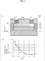
- FIG. 3 is a diagram illustrating a cross-sectional view and a resistance fluctuation rate of resistive element 100a according to Variation 1 of Embodiment 1. More specifically, (a) in FIG. 3 is the cross-sectional view of resistive element 100a and corresponds to the cross-sectional view in (b) in FIG. 1 . (b) in FIG. 3 is a diagram illustrating a relation between a resistance fluctuation rate and a composition ratio of Si/N of first insulating layer 106a when the voltage of 50 V is applied to resistive element 100a.
- Resistive element 100a includes substrate 101, first nitride semiconductor layer 102, second nitride semiconductor layer 103, isolation layer 104, first insulating layer 106a, two-dimensional electron gas layer 107, first electrode 113, and second electrode 114. Resistive element 100a has a resistance-value stabilization structure. In resistive element 100a, a conductive layer is not provided above first insulating layer 106a between first electrode 113 and second electrode 114 in plan view.
- First insulating layer 106a is made of silicon nitride (SiN).
- the composition ratio of Si/N of first insulating layer 106a at an interface between first insulating layer 106a and second nitride semiconductor layer 103 is at least 1.1 and at most 2.3.
- the composition ratio of Si/N of first insulating layer 106a, for example, in a region within 10 nm from the interface is at least 1.1 and at most 2.3.
- the resistance-value stabilization structure according to this variation is a structure in which first insulating layer 106a has the above-described configuration.
- a resistance fluctuation rate is a value indicating a rate of change in resistance values before and after voltage application.
- the composition ratio of Si/N increases, the resistance fluctuation rate is suppressed. This will be explained as follows. With a surplus amount of Si in SiN, Si dangling-bonds are present in a large number and perform oxygen-gettering in a surface oxidized layer that is one of the causes of surface level 108, and this cancels surface level 108. Since surface level 108 is thus canceled, the generation of trapped electrons 109 as illustrated in FIG. 2A is inhibited and the resistance fluctuation rate is suppressed.
- setting the composition ratio of Si/N to at least 1.1 enables the resistance fluctuation rate indicating a value that is sufficiently below 20%.
- the resistance fluctuation rate below 20% can fully meet a required specification of a product.
- Setting the composition ratio of Si/N to at least 1.2 enables the resistance fluctuation rate to be at most 10% and setting the composition ratio of Si/N to at least 1.5 enables the resistance fluctuation rate to be at most 5%. Accordingly, it is possible to fully meet a required specification of a highly-challenging product.
- FIG. 4A illustrates a plan view and a cross-sectional view of field effect transistor 200 formed on the same substrate (substrate 101) that resistive element 100a according to Variation 1 includes. More specifically, (a) in FIG. 4A is the plan view of field effect transistor 200 and (b) in FIG. 4A is the cross-sectional view illustrating a cross section of field effect transistor 200 taken along the line IV-IV in (a) in FIG. 4A .
- Field effect transistor 200 includes substrate 101, first nitride semiconductor layer 102, second nitride semiconductor layer 103, two-dimensional electron gas layer 107, source electrode 110, gate electrode 111, drain electrode 112, first insulating layer 106a, second insulating layer 126, and isolation layer 104.
- resistive element 100a and field effect transistor 200 may be formed at the same time.
- first insulating layer 106a is disposed in contact with the top surface of second nitride semiconductor layer 103.
- Source electrode 110 and drain electrode 112 are disposed in the opening portions of first insulating layer 106a and are ohmically connected to two-dimensional electron gas layer 107.
- Gate electrode 111 that is Schottky-contacted to second nitride semiconductor layer 103 is disposed between source electrode 110 and drain electrode 112. Note that gate electrode 111 may contact second nitride semiconductor layer 103 via a p-n junction. Alternatively, a gate insulating layer may be provided. The gate insulating layer may be inserted between gate electrode 111 and second nitride semiconductor layer 103 to form a metal-insulator-semiconductor (MIS) structure.
- MIS metal-insulator-semiconductor
- second insulating layer 126 is disposed above first insulating layer 106a, source electrode 110, gate electrode 111, and drain electrode 112.
- Second insulating layer 126 is made of SiN.
- Second insulating layer 126 may be made of, for example, SiO 2 , SiON, or AlN.
- Second insulating layer 126 and first insulating layer 106a may, but not limited to, have the same materials and compositions.
- FIG. 4A shows a leak current path between the gate and the drain of field effect transistor 200.
- the leak current path from drain electrode 112 to gate electrode 111 includes two paths, one passing through two-dimensional electron gas layer 107 and the other passing through first insulating layer 106a.
- FIG. 4B is a diagram illustrating a relation between resistivity and a composition ratio of Si/N of first insulating layer 106a according to Variation 1 of Embodiment 1.
- the resistivity decreases with an increase in the composition ratio of Si/N. Therefore, if the composition ratio of Si/N increases too much, the amount of a leak current passing through first insulating layer 106a increases and the amount of a leak current flowing in a reverse direction between the gate and the drain increases.
- Setting the composition ratio of Si/N to be at most 2.3 achieves the resistivity of at least 1.7 ⁇ 10 2 ⁇ cm.
- the amount of the leak current passing through first insulating layer 106a in the reverse direction between the gate and the drain can be reduced to at most 10% of the total amount of the leak currents (i.e., a sum of the leak current passing through two-dimensional electron gas layer 107 and the leak current passing through first insulating layer 106a).
- the composition ratio of Si/N of at most 2.0 achieves the resistivity of at least 3.0 ⁇ 10 2 ⁇ cm, and what is more, the composition ratio of Si/N of at most 1.8 achieves the resistivity of at least 4.0 ⁇ 10 2 ⁇ cm. Accordingly, it is possible to fully meet a required specification of a highly-challenging product.
- the surface level is canceled by Si dangling-bonds, and therefore, the resistance value of two-dimensional electron gas layer 107 is less apt to change. Namely, it is possible to provide resistive element 100a which exhibits a resistance value that is stable with less fluctuation.
- composition ratio of Si/N it is possible to fully meet a required specification of a highly-challenging product.
- the resistance-value stabilization structure according to Variation 1 of Embodiment 1 is a structure in which the composition ratio of Si/N of the insulating layer made of SiN is at least 1.1 and at most 2.3, but a resistance-value stabilization structure according to the present disclosure is not limited to such a structure.
- a resistance-value stabilization structure according to Variation 2 has a first hole injection electrode.
- a resistance-value stabilization structure according to Variation 3 has a first hole injection electrode and a second hole injection electrode. It should be noted that in this embodiment, detailed description of structural elements commonly shared with Embodiment 1 and Variation 1 thereof will be omitted.
- FIG. 5 illustrates cross-sectional views of resistive element 100b according to Variation 2 of Embodiment 1 and resistive element 100c according to Variation 3 of Embodiment 1. More specifically, (a) in FIG. 5 is a cross-sectional view of resistive element 100b according to Variation 2 of Embodiment 1. (b) in FIG. 5 is a cross-sectional view of resistive element 100c according to Variation 3 of Embodiment 1.
- resistive element 100b according to Variation 2 will be described with reference to (a) in FIG. 5 .
- Resistive element 100b according to Variation 2 includes the structural elements included in resistive element 100 according to Embodiment 1 and first hole injection electrode 115.
- a conductive layer is not provided above first insulating layer 106 between first electrode 113 and second electrode 114 in plan view.
- First hole injection electrode 115 is disposed in contact with the top surface of second nitride semiconductor layer 103 on the first electrode 113 side between first electrode 113 and second electrode 114. In this variation, first hole injection electrode 115 is inserted between second nitride semiconductor layer 103 and a portion of first electrode 113, as illustrated in (a) in FIG. 5 . First hole injection electrode 115 is electrically connected to first electrode 113.
- First hole injection electrode 115 is made of p-type GaN.
- First hole injection electrode 115 may be made of, for example, InGaN, AlGaN or AlInGaN that is a p-type group III nitride semiconductor.
- the resistance-value stabilization structure according to this variation is a structure in which first hole injection electrode 115 has the above-described configuration.
- First hole injection electrode 115 injects a hole in second nitride semiconductor layer 103 when the potential of first electrode 113 is higher than that of second electrode 114.
- first electrode 113 With the potential of first electrode 113 being higher than that of second electrode 114, a current flows from first electrode 113 to second electrode 114. Then, a hole is injected from first hole injection electrode 115 and the hole is capable of cancelling trapped electrons 109 trapped to the surface level of second nitride semiconductor layer 103.
- trapped electrons 109 could cause an increase in the resistance value of two-dimensional electron gas layer 107.
- the resistance value of two-dimensional electron gas layer 107 is less apt to change. Namely, it is possible to provide resistive element 100b which exhibits a resistance value that is stable with less fluctuation.
- resistive element 100b it is recommended to use resistive element 100b so that a potential higher than that of second electrode 114 is supplied to first electrode 113. Accordingly, a hole is injected from first hole injection electrode 115 and it is possible to cancel trapped electrons 109 trapped to the surface level of second nitride semiconductor layer 103 and thus achieve resistive element 100b which exhibits a resistance value that is stable with less fluctuation.
- resistive element 100c according to Variation 3 will be described with reference to (b) in FIG. 5 .
- Resistive element 100c according to Variation 3 includes the structural elements included in resistive element 100 according to Embodiment 1, first hole injection electrode 115, and second hole injection electrode 116. In resistive element 100c according to Variation 3, a conductive layer is not provided above first insulating layer 106 between first electrode 113 and second electrode 114 in plan view.
- First hole injection electrode 115 according to Variation 3 has the same configuration as that of first hole injection electrode 115 according to Variation 2.
- Second hole injection electrode 116 is disposed in contact with the top surface of second nitride semiconductor layer 103 on the second electrode 114 side between first electrode 113 and second electrode 114. In this variation, second hole injection electrode 116 is inserted between second nitride semiconductor layer 103 and a portion of second electrode 114, as illustrated in (b) in FIG. 5 . Second hole injection electrode 116 is electrically connected to second electrode 114.
- Second hole injection electrode 116 is made of p-type GaN.
- Second hole injection electrode 116 may be made of, for example, InGaN, AlGaN, or AlInGaN that is a p-type group III nitride semiconductor.
- a resistance-value stabilization structure according to this variation is a structure in which first hole injection electrode 115 and second hole injection electrode 116 each have the above-described configuration.
- Second hole injection electrode 116 injects a hole in second nitride semiconductor layer 103 when the potential of second electrode 114 is higher than that of first electrode 113.
- first electrode 113 being higher than that of second electrode 114
- second hole injection electrode 116 is injected from second hole injection electrode 116.
- the injected hole is capable of cancelling trapped electrons 109 trapped to the surface level of second nitride semiconductor layer 103.
- a hole is injected from either of the two electrodes (first electrode 113 and second electrode 114).
- the resistance value of two-dimensional gas layer 107 is less apt to change.
- resistive element 100c which exhibits a resistance value that is stable with less fluctuation.
- resistive element 100c allows hole injection from either of the two electrodes and can be used as an element that allows a current to flow bidirectionally.
- a resistance-value stabilization structure according to the present disclosure is not limited to the structure described in the aforementioned Embodiment 1 or any one of the variations thereof.
- a resistance-value stabilization structure according to Variation 4 has a first electron extraction electrode.
- a resistance-value stabilization structure according to Variation 5 has a first electron extraction electrode and a second electron extraction electrode. Note that in these variations, detailed description of structural elements commonly shared with Embodiment 1 and the variations thereof will be omitted.
- FIG. 6 illustrates cross-sectional views of resistive element 100d according to Variation 4 of Embodiment 1 and resistive element 100e according to Variation 5 of Embodiment 1. More specifically, (a) in FIG. 6 is a cross-sectional view of resistive element 100d according to Variation 4. (b) in FIG. 6 is a cross-sectional view of resistive element 100e according to Variation 5 of Embodiment 1.
- resistive element 100d according to Variation 4 will be described with reference to (a) in FIG. 6 .
- Resistive element 100d according to Variation 4 includes the structural elements included in resistive element 100 according to Embodiment 1 and first electron extraction electrode 117. In resistive element 100d according to Variation 4, a conductive layer is not provided above first insulating layer 106 between first electrode 113 and second electrode 114 in plan view.
- First electron extraction electrode 117 is disposed in contact with the top surface of second nitride semiconductor layer 103 on the first electrode 113 side between first electrode 113 and second electrode 114. In this variation, first electron extraction electrode 117 is inserted between second nitride semiconductor layer 103 and a portion of first electrode 113. First electron extraction electrode 117 is electrically connected to first electrode 113.
- First electron extraction electrode 117 is Schottky-contacted to second nitride semiconductor layer 103.
- First electron extraction electrode 117 has a layered structure including Ni.
- First electron extraction electrode 117 may have, for example, a layered structure including at least one of Ti, TiN, Hf, Pd, or Pt.
- the resistance-value stabilization structure according to this variation is a structure in which first electron extraction electrode 117 has the above-described configuration.
- First electron extraction electrode 117 extracts electrons from second nitride semiconductor layer 103 when the potential of first electrode 113 is higher than that of second electrode 114.
- first electrode 113 With the potential of first electrode 113 being higher than that of second electrode 114, a current flows from first electrode 113 to second electrode 114. This enables first electron extraction electrode 117, which is Schottky-contacted to second nitride semiconductor layer 103, to extract trapped electrons 109 trapped to the surface level.
- trapped electrons 109 could cause an increase in the resistance value of two-dimensional electron gas layer 107.
- the resistance value of two-dimensional electron gas layer 107 is less apt to change. Namely, it is possible to provide resistive element 100d which exhibits a resistance value that is stable with less fluctuation.
- resistive element 100e according to Variation 5 will be described with reference to (b) in FIG. 6 .
- Resistive element 100e according to Variation 5 includes the structural elements included in resistive element 100 according to Embodiment 1, first electron extraction electrode 117, and second electron extraction electrode 118. In resistive element 100e according to Variation 5, a conductive layer is not provided above first insulating layer 106 between first electrode 113 and second electrode 114 in plan view.
- First electron extraction electrode 117 according to Variation 5 has the same configuration as that of first electron extraction electrode 117 according to Variation 4.
- Second electron extraction electrode 118 is disposed in contact with the top surface of second nitride semiconductor layer 103 on the second electrode 114 side between first electrode 113 and second electrode 114. In this variation, second electron extraction electrode 118 is inserted between second nitride semiconductor layer 103 and a portion of second electrode 114, as illustrated in (b) in FIG. 6 . Second electron extraction electrode 118 is electrically connected to second electrode 114.
- Second electron extraction electrode 118 has a layered structure including Ni.
- Second electron extraction electrode 118 may have, for example, a layered structure including at least one of Ti, TiN, Hf, Pd, or Pt.
- the resistance-value stabilization structure according to this variation is a structure in which first electron extraction electrode 117 and second electron extraction electrode 118 each have the above-described configuration.
- Second electron extraction electrode 118 extracts electrons from second nitride semiconductor layer 103 when the potential of second electrode 114 is higher than that of first electrode 113.
- first electron extraction electrode 117 extracts electrons
- second electron extraction electrode 118 extracts electrons
- the resistance value of two-dimensional electron gas layer 107 is less apt to change.
- resistive element 100e which exhibits a resistance value that is stable with less fluctuation.
- a resistance-value stabilization structure according to the present disclosure is not limited to the structure described in the aforementioned Embodiment 1 or any one of the variations thereof.
- a resistance-value stabilization structure according to Variation 6 has a stress buffer layer. Note that in this variation, detailed description of structural elements commonly shared with Embodiment 1 and the variations thereof will be omitted.
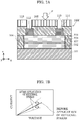
- FIG. 7A is a cross-sectional view of resistive element 100f according to Variation 6 of Embodiment 1. Stress P that is externally applied to resistive element 100f is illustrated in FIG. 7A .
- Resistive element 100f according to Variation 6 includes the structural elements included in resistive element 100 according to Embodiment 1 and stress buffer layer 119. In resistive element 100f according to Variation 6, a conductive layer is not provided above first insulating layer 106 between first electrode 113 and second electrode 114 in plan view.
- Stress buffer layer 119 is disposed above first insulating layer 106.
- the plan-view shape of stress buffer layer 119 may match the plan-view shape of first insulating layer 106.
- Stress buffer layer 119 is a layer for buffering stress that is externally applied to resistive element 100f.
- the resistance-value stabilization structure according to this variation is a structure in which stress buffer layer 119 has the above-described configuration.
- resistive element 100f stress externally applied to resistive element 100f.
- stress is externally applied to resistive element 100f, for example, when a sealing material to be used for a semiconductor chip assembly is formed.
- FIG. 7B how the stress affects the current-voltage characteristics of resistive element 100f.
- FIG. 7B is a conceptual diagram illustrating current-voltage characteristics of resistive element 100f according to Variation 6 of Embodiment 1 before and after stress is externally applied.
- two-dimensional electron gas layer 107 generated on the GaN layer (first nitride semiconductor layer 102) side at an interface between AlGaN (second nitride semiconductor layer 103) and GaN (first nitride semiconductor layer 102) is caused by piezo-polarized charges. Therefore, when stress is applied to resistive element 100f, the carrier concentration of two-dimensional electron gas layer 107 changes and the resistance value of two-dimensional electron gas layer 107 fluctuates.
- Stress buffer layer 119 is made of polyimide. Stress buffer layer 119 may be made of, for example, a fluorine resin or a benzocyclobutene (BCB) resin, or formed of a photosensitive insulating layer or the like. Alternatively, stress buffer layer 119 may be made of a material having elasticity in an amount enough to buffer stress P that is externally applied to resistive element 100f.
- the resistance-value stabilization structure according to this variation is a structure in which stress buffer layer 119 has the above-described configuration.
- resistive element 100f which exhibits a resistance value that is stable with less fluctuation.
- a resistance-value stabilization structure according to the present disclosure is not limited to the structure described in the aforementioned Embodiment 1 or any one of the variations thereof.
- a resistance-value stabilization structure according to Variation 7 has an isolation layer that is disposed to surround a first nitride semiconductor layer and that includes inactive ions. Note that in this variation, detailed description of structural elements commonly shared with Embodiment 1 and the variations thereof will be omitted.
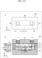
- FIG. 8A is a diagram illustrating a migration of inactive ions in resistive element 100 according to Embodiment 1. More specifically, (a) in FIG. 8A is a plan view of resistive element 100. (b) in FIG. 8A is a cross-sectional view illustrating a cross section, which is taken along the line VIII-VIII in (a) in FIG. 8A , of resistive element 100 before inactive ions migrate. (c) in FIG. 8A is a cross-sectional view illustrating a cross section, which is taken along the line VIII-VIII in (a) in FIG. 8A , of resistive element 100 after inactive ions migrate. Note that inactive-ions migration directions M are indicated by arrows in (c) in FIG. 8A .
- Inactive ions implanted for isolation may migrate due to heat treatment.
- migrating inactive ions reach two-dimensional electron gas layer 107, ion migration region 120 to which the inactive ions have migrated is formed in resistive element 100. Since the inactive ions that have migrated inactivate carriers in two-dimensional electron gas layer 107, this narrows the region of an electric resistance element that functions as an electrical resistive component.
- FIG. 8B is a conceptual diagram illustrating current-voltage characteristics of resistive element 100 according to Embodiment 1 before and after inactive ions migrate. As described above, since the carrier concentration of two-dimensional electron gas layer 107 decreases due to the migration of inactive ions, the resistance value of resistive element 100 may increase.
- a resistance-value stabilization structure is a structure related to an isolation layer.
- FIG. 9 illustrates a plan view and a cross-sectional view of resistive element 100g according to Variation 7 of Embodiment 1. More specifically, (a) in FIG. 9 is the plan view of resistive element 100g and (b) in FIG. 9 is the cross-sectional view illustrating a cross section of resistive element 100g taken along the line IX-IX in (a) in FIG. 9 .
- Resistive element 100g includes substrate 101, first nitride semiconductor layer 102, second nitride semiconductor layer 103, isolation layer 104g, first insulating layer 106g, two-dimensional electron gas layer 107, first electrode 113, and second electrode 114. Resistive element 100g has a resistance-value stabilization structure. In resistive element 100g, a conductive layer is not provided above first insulating layer 106g between first electrode 113 and second electrode 114 in plan view.
- Isolation layer 104g is disposed to surround first nitride semiconductor layer 102 in the plan view and includes inactive ions. Moreover, distance d1 between the top surface of isolation layer 104g and the top surface of substrate 101 is less than distance d2 between the bottom surface of two-dimensional electron gas layer 107 and the top surface of substrate 101. In other words, in this variation, isolation layer 104g is not in contact with two-dimensional electron gas layer 107.
- the resistance-value stabilization structure according to this variation is a structure in which isolation layer 104g has the above-described configuration.
- first insulating layer 106g may be disposed to cover the top surface of second nitride semiconductor layer 103 and lateral surfaces of first nitride semiconductor layer 102, two-dimensional electron gas layer 107, and second nitride semiconductor layer 103.
- Such resistive element 100g is manufactured as in the following example. First, first nitride semiconductor layer 102 and second nitride semiconductor layer 103 are sequentially stacked on the top surface of substrate 101 (two-dimensional electron gas layer 107 is also formed in this process). Next, a portion of first nitride semiconductor layer 102 and a portion of second nitride semiconductor layer 103 are etched.
- first nitride semiconductor layer 103 and first nitride semiconductor layer 102 in a region extending from the top surface of second nitride semiconductor layer 103 to the middle of first nitride semiconductor layer 102 are etched so that two-dimensional electron gas layer 107 is exposed at the lateral surface of first nitride semiconductor layer 102.
- mesa structure 122 is formed in first nitride semiconductor layer 102 and second nitride semiconductor layer 103.
- ions are implanted in first nitride semiconductor layer 102 that remains after the etching.
- isolation layer 104g is formed.
- resistive element 100g since there is no chance that an ion-implanted region (i.e., isolation layer 104g) comes in contact with two-dimensional electron gas layer 107, it is possible to suppress the migration of inactive ions to two-dimensional electron gas layer 107. Namely, it is possible to provide resistive element 100g which exhibits a resistance value that is stable with less fluctuation.
- a resistance-value stabilization structure according to the present disclosure is not limited to the structure described in the aforementioned Embodiment 1 or any one of the variations thereof.
- a resistance-value stabilization structure according to Variation 8 has a high resistance layer. Note that in this variation, detailed description of structural elements commonly shared with Embodiment 1 and the variations thereof will be omitted.
- FIG. 10A is a diagram illustrating electrical resistances in resistive element 100 according to Embodiment 1. More specifically, (a) in FIG. 10A is a plan view of resistive element 100. (b) in FIG. 10A is a cross-sectional view illustrating a cross section of resistive element 100 taken along the line X-X in (a) in FIG. 10A .
- a current path of resistive element 100 that includes two-dimensional electron gas layer 107 as an electric resistance element is a path passing through one of first electrode 113 and second electrode 114, two-dimensional electron gas layer 107, and the other of first electrode 113 and second electrode 114.
- first electrode 113 and second electrode 114 when substrate 101 is an Si substrate, the resistance value of substrate 101 decreases at high temperature. Therefore, a current path passing through one of first electrode 113 and second electrode 114, substrate 101, and the other of first electrode 113 and second electrode 114 may be newly generated as a current path of resistive element 100 that includes two-dimensional electron gas layer 107 as an electric resistance element.
- FIG. 10B is a conceptual diagram illustrating current-voltage characteristics of resistive element 100 according to Embodiment 1 at ordinary temperature or at high temperature.
- the resistance value of resistive element 100 at high temperature may be lower than that at ordinary temperature, and as a result, the current value of resistive element 100 at high temperature may become higher than that at ordinary temperature.
- the resistance-value stabilization structure according to this variation is a structure related to a high resistance layer.
- FIG. 11 illustrates a cross-sectional view of resistive element 100h according to Variation 8 of Embodiment 1. More specifically, FIG. 11 is a diagram corresponding to the cross-sectional view in (b) in FIG. 1 .
- Resistive element 100h according to this variation includes the structural elements included in resistive element 100 according to Embodiment 1 and high resistance layer 123. In resistive element 100h according to this variation, a conductive layer is not provided above first insulating layer 106 between first electrode 113 and second electrode 114 in plan view.
- High resistance layer 123 is disposed between substrate 101 and first nitride semiconductor layer 102.
- High resistance layer 123 has electrical resistivity higher than that of substrate 101.
- the electrical resistivity of high resistance layer 123 may be, for example, at least 1000 ⁇ cm.
- High resistance layer 123 may be a layer (e.g., an AlGaN layer or an AlN layer) having a band gap larger than that of first nitride semiconductor layer 102 or may be a layer having a super-lattice structure including both AlN and AlGaN.
- high resistance layer 123 may be a layer formed by injecting, with high acceleration, a light element such as helium or hydrogen into a region on the substrate 101 side in first nitride semiconductor layer 102, or may be an insulating layer formed on the top surface of substrate 101 by an epitaxial method.
- the resistance-value stabilization structure according to this variation is a structure in which high resistance layer 123 has the above-described configuration.
- resistive element 100h which exhibits a resistance value that is stable with less fluctuation.
- a resistance-value stabilization structure according to the present disclosure is not limited to the aforementioned Embodiment 1 or any one of the variations thereof.
- a resistance-value stabilization structure according to Variation 9 has a low temperature-characteristic resistive element portion. Note that in this variation, detailed description of structural elements commonly shared with Embodiment 1 and the variations thereof will be omitted.
- a resistive element that includes a two-dimensional electron gas layer as a resistance element is characterized by a large increase of its resistance value caused by temperature rise (i.e., the temperature coefficient of the two-dimensional electron gas layer is high), as mentioned in PTL 1. This is because the mobility of the two-dimensional electron gas layer decreases with temperature rise. With a circuit configuration advantageously utilizing such a change, the aforementioned increase in resistance value is not a problem, but it becomes one in the case of using a two dimensional electron gas layer simply as a resistive element which exhibits a constant value.
- FIG. 12 illustrates a plan view and a cross-sectional view of resistive element 100i according to Variation 9 of Embodiment 1. More specifically, (a) in FIG. 12 is the plan view of resistive element 100i and (b) in FIG. 12 is the cross-sectional view illustrating a cross section of resistive element 100i taken along the line XII-XII in (a) in FIG. 12 .
- Resistive element 100i according to this variation includes the structural elements included in resistive element 100 according to Embodiment 1, low temperature-characteristic resistive element portion 300, and two interconnect layers 125.
- a conductive layer is not provided above first insulating layer 106 between first electrode 113 and second electrode 114 in plan view.
- Low temperature-characteristic resistive element portion 300 is disposed above substrate 101. As illustrated in FIG. 12 , low temperature-characteristic resistive element portion 300 includes isolation layer 104, first insulating layer 106, thin-film resistive layer 124, third electrode 130, and fourth electrode 131.
- Thin-film resistive layer 124 is disposed above isolation layer 104 and is made of a material having a temperature coefficient lower than that of two-dimensional electron gas layer 107.
- Thin-film resistive layer 124 is, for example, a metal resistance made of TiN.
- Thin-film resistive layer 124 may be, for example, made of Al, Au, W, Ti, Mo, Ta, TaN, Pt, Pd, Ni, Cr, Fe, Ag, Cu, SiN, or AlN.
- Thin-film resistive layer 124 may be a semiconductor resistance made of Si having a negative temperature coefficient.
- Thin-film resistive layer 124 may be made of, for example, SiN or WSiN having a high composition ratio of Si. The width, thickness, and length of thin-film resistive layer 124 are determined so that a desired resistance value can be obtained.
- Third electrode 130 and fourth electrode 140 are stacked above thin-film resistive layer 124.
- Third electrode 130 and fourth electrode 131 are leading electrodes disposed above thin-film resistive layer 124. A space is provided between third electrode 130 and fourth electrode 131 in the plan view. Third electrode 130 and fourth electrode 131 are electrically connected to thin-film resistive layer 124.
- Third electrode 130 and fourth electrode 131 are made of a material having electrical conduction.
- Third electrode 130 and fourth electrode 131 may be made of, for example, metal.
- third electrode 130 and fourth electrode 131 may each have a layered structure including at least one of Ti, Al, Cr, or Au. Note that third electrode 130 and fourth electrode 131 may, but not limited to, be made of the same material.
- First insulating layer 106 is disposed between third electrode 130 and fourth electrode 131 in the plan view and in contact with the top surface of isolation layer 104. First insulating layer 106 is disposed to surround thin-film resistive layer 124, third electrode 130, and fourth electrode 131.
- the temperature coefficient of low temperature-characteristic resistive element portion 300 thus configured is lower than that of two-dimensional electron gas layer 107 (an increase in resistance value due to temperature rise is small). Alternatively, the temperature coefficient of low temperature-characteristic resistive element portion 300 becomes negative (the resistance value decreases due to temperature rise).
- the temperature coefficient of low temperature-characteristic resistive element portion 300 is lower than that of two-dimensional electron gas layer 107. Namely, even at high temperature, the resistance value of low temperature-characteristic resistive element portion 300 is less apt to increase than that of two-dimensional electron gas layer 107.
- First electrode 113 is connected to third electrode 130 and second electrode 114 is connected to fourth electrode 131.
- the electrodes are connected by two interconnect layers 125.
- one of two interconnect layers 125 connects first electrode 131 to third electrode 130 and the other of two interconnect layers 125 connects second electrode 114 to fourth electrode 131.
- first electrode 113, two-dimensional electron gas layer 107, and second electrode 114 are connected to low temperature-characteristic resistive element portion 300 in parallel in this variation.
- Two interconnect layers 125 may be disposed above and over first insulating layer 106 and thus connect first electrode 113 to third electrode 130 and second electrode 114 to fourth electrode 131, respectively.
- Two interconnect layers 125 are disposed apart from each other.
- Two interconnect layers 125 are made of a material having electrical conduction.
- Two interconnect layers 125 may be made of, for example, metal.
- Two interconnect layers 125 may each have a layered structure including, for example, at least one of Al, Au, Ag, or Cu. Note that two interconnect layers 125 may, but not limited to, be made of the same material.
- the resistance-value stabilization structure according to this variation is a structure in which low temperature-characteristic resistive element portion 300 has the above-described configuration.
- a resistance value obtained by merging the electric resistance element of two-dimensional electron gas layer 107 and low temperature-characteristic resistive element portion 300 is less apt to change even at high temperature, compared to the resistance value of the electric resistance element of two-dimensional electron gas layer 107 alone.
- resistive element 100i which exhibits a resistance value that is stable with less fluctuation.
- a resistance-value stabilization structure according to the present disclosure is not limited to the structure described in the aforementioned Embodiment 1 or any one of the variations thereof.
- a resistance-value stabilization structure according to Variation 10 is a structure related to a first electrode and a second electrode. Note that in this variation, detailed description of structural elements commonly shared with Embodiment 1 and the variations thereof will be omitted.
- FIG. 13 illustrates a plan view and a cross-sectional view of resistive element 100j according to Variation 10 of Embodiment 1. More specifically, (a) in FIG. 13 is the plan view of resistive element 100j and (b) in FIG. 13 is the cross-sectional view illustrating a cross section of resistive element 100j taken along the line XIII-XIII in (a) in FIG. 13 .
- Resistive element 100j includes substrate 101, first nitride semiconductor layer 102, second nitride semiconductor layer 103, isolation layer 104, first insulating layer 106, two-dimensional electron gas layer 107, first electrode 113j, and second electrode 114j. Resistive element 100j has a resistance-value stabilization structure. In resistive element 100j, a conductive layer is not provided above insulating layer 106 between first electrode 113j and second electrode 114j in plan view.
- each of first electrode 113j and second electrode 114j has an embedded portion extending from the top surface of second nitride semiconductor layer 103 and including a portion of first nitride semiconductor layer 102 such that the electrode contacts two-dimensional electron gas layer 107.
- a portion, of first electrode 113j or second electrode 114j, which extends from the top surface of second nitride semiconductor layer 103 and reaches two-dimensional electron gas layer 107 is embedded.
- two-dimensional electron gas layer 107 between first electrode 113j and second electrode 114j that are disposed apart from each other in the plan view is a resistance element.
- the resistance-value stabilization structure according to this variation is a structure in which first electrode 113j and second electrode 114j have the above-described configuration.
- the resistance value of two-dimensional electron gas layer 107 is less apt to depend on the sizes of first electrode 113j and second electrode 114j.
- resistive element 100j which exhibits a resistance value that is stable with less fluctuation.
- a resistance-value stabilization structure according to the present disclosure is not limited to the aforementioned Embodiment 1 or any one of the variations thereof.
- a resistance-value stabilization structure according to Variation 11 is a structure related to a first insulating layer. Note that in this variation, detailed description of structural elements commonly shared with Embodiment 1 and the variations thereof will be omitted.
- FIG. 14 illustrates a plan view and a cross-sectional view of resistive element 100k according to Variation 11 of Embodiment 1. More specifically, (a) in FIG. 14 is the plan view of resistive element 100k and (b) in FIG. 14 is the cross-sectional view illustrating a cross section of resistive element 100k taken along the line XIV-XIV in (a) in FIG. 14 .
- Resistive element 100k includes substrate 101, first nitride semiconductor layer 102, second nitride semiconductor layer 103, isolation layer 104, first insulating layer 106k, second insulating layer 126, two-dimensional electron gas layer 107, first electrode 113, and second electrode 114. Resistive element 100k has a resistance-value stabilization structure. In resistive element 100k, a conductive layer is not provided above insulating layer 106k between first electrode 113 and second electrode 114 in plan view.
- first insulating layer 106k is disposed apart from first electrode 113 and second electrode 114. In other words, first insulating layer 106k is neither in contact with first electrode 113 nor with second electrode 114.
- Second insulating layer 126 is disposed above second nitride semiconductor layer 103 to fill a space between first insulating layer 106k and first electrode 113 and a space between first insulating layer 106k and second electrode 114. Moreover, second insulating layer 126 is disposed to surround first electrode 113 and second electrode 114 in the plan view.
- Second insulating layer 126 may be disposed above first insulating layer 106k. As illustrated in (b) in FIG. 14 , second insulating layer 126 is provided neither above first electrode 113 nor above second electrode 114, and opening portions are provided. For this reason, the top surfaces of first electrode 113 and second electrode 114 are exposed.
- Second insulating layer 126 is made of SiN. Second insulating layer 126 may be made of, for example, SiO 2 , SiON, or AlN. Second insulating layer 126 and first insulating layer 106k may, but not limited to, have the same materials and the same compositions.
- the resistance-value stabilization structure according to this variation is a structure in which first insulating layer 106k has the above-described configuration.
- a method of manufacturing resistive element 100k according to this variation will be briefly described herein.
- Heat treatment of approximately 500 Celsius degrees is required for ohmically connecting first electrode 113 and second electrode 114 to two-dimensional electron gas layer 107.
- metal constituting first electrode 113 and second electrode 114 may be heat dissipated throughout first insulating layer 106k during the heat treatment.
- this might affect the reliability of resistive element 100k and causes a problem such as a short circuit between first electrode 113 and second electrode 114 or a decrease in a breakdown voltage of first insulating layer 106k.
- first insulating layer 106k is formed so as not to contact first electrode 113 and second electrode 114 and the heat treatment is subsequently carried out, as in the above-described configuration. After that, second insulating layer 126 is formed.
- Embodiment 1 The following describes a power amplifier circuit for which the resistive element according to Embodiment 1 or any one of the variations thereof is used. It should be noted that in this embodiment, detailed description of structural elements commonly shared with Embodiment 1 and the variations thereof will be omitted.
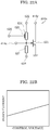
- FIG. 15A is a circuit diagram illustrating power amplifier circuit 500 according to Embodiment 2.
- FIG. 15B is a diagram illustrating temperature dependence of a gain of power amplifier circuit 500 according to Embodiment 2. Note that a temperature indicated in FIG. 15B is a temperature of power amplifier circuit 500.
- Power amplifier circuit 500 includes resistive element 100 according to Embodiment 1, and field effect transistor 401 that is disposed above substrate 101 included in resistive element 100, and capacitor 403.
- Field effect transistor 401 includes a source electrode, a drain electrode, and a gate electrode.
- One of first electrode 113 and second electrode 114 included in resistive element 100 is electrically connected to the gate electrode whereas the other of first electrode 113 and second electrode 114 is electrically connected to the drain electrode via capacitor 403.
- Power amplifier circuit 500 may include gate terminal 404 and drain terminal 405 electrically connected to the gate electrode and the drain electrode of field effect transistor 401, respectively, and resistance 402.
- resistive element 100 is resistance 402 illustrated in FIG. 15A .
- a negative feedback circuit which attenuates an output signal with feedback resistance to feedback-input the signal to an input side, is used for the stabilization of a radio frequency circuit.
- the negative feedback circuit when a feedback resistance value decreases, the stability of power amplifier circuit 500 increases and the gain of power amplifier circuit 500 decreases.
- a negative feedback circuit including resistance 402 and capacitor 403 is connected to gate terminal 404 and drain terminal 405 of field effect transistor 401 for signal amplifier.
- the gain of power amplifier circuit 500 that uses semiconductors decreases due to a decrease in carrier mobility at high temperature.
- a gain fall at high temperature is large, as illustrated in FIG. 15B .
- Power amplifier circuit 500 has resistive element 100 including two-dimensional electron gas layer 107 having a high temperature coefficient. Accordingly, in power amplifier circuit 500, the resistance value of two-dimensional electron gas layer 107 increases at high temperature and an amount of feedback in the negative feedback circuit gets smaller, and this moderates a gain fall at high temperature.
- Embodiment 2 the resistive element is included in the negative feedback circuit, but a resistive element according to the present disclosure is not limited to such a resistive element.
- a resistive element is included in a bias circuit that supplies a gate voltage to a field effect transistor to set a drain current of the field effect transistor. It should be noted that in this embodiment, detailed description of structural elements commonly shared with Embodiment 1 and the variations thereof will be omitted.
- FIG. 16A is a circuit diagram illustrating power amplifier circuit 500a according to Embodiment 3.
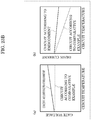
- FIG. 16B is a diagram illustrating temperature dependences of a gate voltage and a drain current of field effect transistor 406 included in power amplifier circuit 500a according to Embodiment 3. More specifically, (a) in FIG. 16B illustrates temperature dependence of the gate voltage of field effect transistor 406 while (b) in FIG. 16B illustrates temperature dependence of the drain current of field effect transistor 406. Note that a temperature indicated in FIG. 16B is a temperature of power amplifier circuit 500a.
- Power amplifier circuit 500a includes field effect transistor 406 and a bias circuit.
- Power amplifier circuit 500a may include first gate bias terminal 407, second gate bias terminal 408, first resistance 409, second resistance 410, and gate terminal 404a and drain terminal 405a connected to the gate electrode and the drain electrode of field effect transistor 406, respectively.
- the bias circuit includes resistive element 100 described in Embodiment 1.
- the bias circuit supplies a gate voltage to field effect transistor 406 to set a drain current of field effect transistor 406.
- Resistive element 100 is at least one of first resistance 409 or second resistance 410.
- Field effect transistor 406 is disposed above substrate 101 included in resistive element 100.
- Field effect transistor 406 includes a source electrode, a drain electrode, and a gate electrode.
- a voltage higher than that of second gate bias terminal 408 may be applied to first gate bias terminal 407 and one of first gate bias terminal 407 and second gate bias terminal 408 may be grounded.
- second resistance 410 is resistive element 100 and the temperature coefficient of first resistance 409 is lower than that of second resistance 410.
- the gate voltage of field effect transistor 406 rises due to temperature rise and it is possible to increase the drain current of field effect transistor 406 at high temperature, compared to a case where the temperature coefficients of first resistance 409 and second resistance 410 are same, as illustrated in FIG. 16B .
- first resistance 409 is resistive element 100 and the temperature coefficient of first resistance 409 is higher than that of second resistance 410.
- the gate voltage of field effect transistor 406 decreases due to temperature rise and it is possible to decrease the drain current of field effect transistor 406 at high temperature, compared to the case where the temperature coefficients of first resistance 409 and second resistance 410 are same.
- first resistance 409 and second resistance 410 may be each resistive element 100. Note that in this case, the temperature coefficient of first resistance 409 may be different from that of second resistance 410.
- Embodiment 1 or each of the variations thereof has illustrated an example of the resistive element in which a conductive layer is not provided above the first insulating layer between the first electrode and the second electrode in plan view
- a resistive element according to the present disclosure is not limited to this example.
- a resistive element according to Embodiment 4 includes a conduction control layer and is thus different from the resistive element described in Embodiment 1. It should be noted that in this embodiment, detailed description of structural elements commonly shared with Embodiment 1 and the variations thereof will be omitted.
- FIG. 17 illustrates a plan view and a cross-sectional view of resistive element 100m according to Embodiment 4. More specifically, (a) in FIG. 17 is the plan view of resistive element 100m and (b) in FIG. 17 is the cross-sectional view illustrating a cross section of resistive element 100m taken along the line XVII-XVII in (a) in FIG. 17 .
- Resistive element 100m includes resistive element portion 1000 and a conduction control layer (hereinafter referred to as first conduction control layer 127). Resistive element 100m has a resistance-value stabilization structure. Resistive element portion 1000 includes substrate 101, first nitride semiconductor layer 102, second nitride semiconductor layer 103, isolation layer 104, first insulating layer 106, two-dimensional electron gas layer 107, first electrode 113, and second electrode 114.
- First conduction control layer 127 is disposed above an insulating layer (first insulating layer 106) between first electrode 113 and second electrode 114 in plan view. Note that first conduction control layer 127 may be disposed in a region above second nitride semiconductor layer 103 and between first electrode 113 and second electrode 114 in the plan view. A length of first conduction control layer 127 in a direction in which first electrode 113 and second electrode 114 are aligned in the plan view (i.e., a length in the x-axis direction in FIG. 17 ) is at least half the space between first electrode 113 and second electrode 114. The length of first conduction control layer 127 in the aforementioned direction may be at least the third-fourths of the space between first electrode 113 and second electrode 114, as illustrated in FIG. 17 .
- First conduction control layer 127 supplies an electric field to two-dimensional electron gas layer 107 to control the resistance value of an electric resistance element, in accordance with a voltage supplied from a source outside of resistive element portion 1000.
- first conduction control layer 127 is capable of intentionally controlling the resistance value of the electric resistance element.
- FIG. 18 is a diagram illustrating a situation in which two-dimensional electron gas layer 107 is generated when a potential is supplied to first conduction control layer 127 in resistive element 100m according to Embodiment 4. More specifically, (a) in FIG. 18 is a diagram illustrating a case where a positive potential is supplied to first conduction control layer 127, and (b) in FIG. 18 is a diagram illustrating a case where a negative potential is supplied to first conduction control layer 127. For example, when a positive potential is supplied to first conduction control layer 127 a conduction band at an interface between first nitride semiconductor layer 102 and second nitride semiconductor layer 103 falls below a Fermi level, as illustrated in (a) in FIG.
- resistive element 100m having a desired resistance value.
- resistive element 100m according to this embodiment is a variable resistive element.
- a voltage is supplied to first conduction control layer 127 from a source outside of resistive element portion 1000.
- first conduction control layer 127 may be supplied with a fixed potential or a control potential from a source outside of resistive element portion 1000.
- the potential supplied to first conduction control layer 127 may be a ground potential.
- a voltage is supplied neither from first electrode 113 nor from second electrode 114.
- first conduction control layer 127 is not the gate electrode of a field effect transistor. As described above, first conduction control layer 127 supplies an electric field to two-dimensional electron gas layer 107 to control the resistance value of an electric resistance element, but does not block conduction between first electrode 113 and second electrode 114. Resistive element 100m is therefore not a normally-off field effect transistor.
- first conduction control layer 127 is disposed above first insulating layer 106 and is isolated from second nitride semiconductor layer 103, resistive element 100m is not a junction field effect transistor. Accordingly, a potential to be supplied to first conduction control layer 127 for controlling the resistance value of resistive element 100m needs to be very low and resistive element 100m is thus a variable resistive element readily utilized for a control circuit.
- first conduction control layer 127 in the direction in which first electrode 113 and second electrode 114 are aligned is, the larger an area that first conduction control layer 127 covers two-dimensional electron gas layer 107 gets. Therefore, the longer the length of first conduction control layer 127 is, the more allowed it is to readily supply an electric field to two-dimensional electron gas layer 107. It is thus possible to more easily control the resistance value of two-dimensional electron gas layer 107.
- the resistance-value stabilization structure described in Embodiment 1 or any one of the variations thereof may be used for the resistance-value stabilization structure according to this embodiment.
- the resistance value of two-dimensional electron gas layer 107 is set to a desired value, and what is more, the resistance-value stabilization structure is used to stabilize the resistance value that has been set to the desired value.
- Embodiment 4 has illustrated an example of the resistive element that includes a single conduction control layer, a resistive element according to the present disclosure is not limited to this example. This variation is different from Embodiment 4 in that a resistive element includes a plurality of conduction control layers. Note that in this variation, detailed description of structural elements commonly shared with Embodiment 4 will be omitted.
- FIG. 19 illustrates a plan view and a cross-sectional view of resistive element 100n according to Variation 1 of Embodiment 4. More specifically, (a) in FIG. 19 is the plan view of resistive element 100n, and (b) in FIG. 19 is the cross-sectional view illustrating a cross section of resistive element 100n taken along the line XIX-XIX in (a) in FIG. 19 .
- Resistive element 100n includes the structural elements included in resistive element 100m according to Embodiment 4, second insulating layer 126, and second conduction control layer 128.
- Second insulating layer 126 is disposed above first insulating layer 106 and first conduction control layer 127. As illustrated in FIG. 19 , second insulating layer 126 is disposed to cover first conduction control layer 127. Second insulating layer 126 is disposed to surround first electrode 113 and second electrode 114 in plan view. As illustrated in (b) in FIG. 19 , second insulating layer 126 is provided neither above first electrode 113 nor above second electrode 114 and opening portions are provided. For this reason, the top surfaces of first electrode 113 and second electrode 114 are exposed.
- Second insulating layer 126 is made of SiN. Second insulating layer 126 may be made of, for example, SiO 2 , SiON, or AlN. Second insulating layer 126 and first insulating layer 106 may, but not limited to, have the same materials and the same compositions.
- Second conduction control layer 128 is disposed on an insulating layer (second insulating layer 126) between first electrode 113 and second electrode 114 in the plan view.
- a length of second conduction control layer 128 in a direction in which first electrode 113 and second electrode 114 are aligned (a length in the x-axis direction in FIG. 19 ) in the plan view is at least half the space between first electrode 113 and second electrode 114.
- first conduction control layer 127 and second conduction control layer 128 may be disposed to overlap each other.
- Second conduction control layer 128 supplies an electric field to two-dimensional electron gas layer 107 to control the resistance value of an electric resistance element, in accordance with a voltage supplied from a source outside of resistive element portion 1000.
- the resistance value of two-dimensional electron gas layer 107 indicates any value, as described in Embodiment 4.
- resistive element 100n having a desired resistance value. It can be also said that resistive element 100n according to this embodiment is a variable resistive element.
- second conduction control layer 128 may be substantially same as or different from the potential of first conduction control layer 127.
- resistive element 100n and field effect transistor 200n according to this variation are provided on the same substrate (substrate 101 in this variation).
- FIG. 20 illustrates a plan view and a cross-sectional view of resistive element 100n and field effect transistor 200n according to Variation 1 of Embodiment 4. More specifically, (a) in FIG. 20 is the plan view illustrating resistive element 100n and field effect transistor 200n, and (b) in FIG. 20 is the cross-sectional view illustrating a cross section of resistive element 100n and a cross section of field effect transistor 200n which are taken along the line XX-XX in (a) in FIG. 20 .
- Field effect transistor 200n is disposed above substrate 101 included in resistive element 100n.
- resistive element 100n and field effect transistor 200n are each a one-chip semiconductor that is provided on the same substrate.
- Field effect transistor 200n includes substrate 101, first nitride semiconductor layer 102, second nitride semiconductor layer 103, two-dimensional electron gas layer 107, source electrode 110, gate electrode 111, drain electrode 112, first insulating layer 106, second insulating layer 126, isolation layer 104, and field plate electrode 129.
- resistive element 100n and field effect transistor 200n are electrically isolated from each other by isolation layer 104.
- Field plate electrode 129 alleviates electric field concentration to increase the withstand voltage of field effect transistor 200n.
- resistive element 100n and field effect transistor 200n may be formed at the same time, as illustrated in FIG. 20 .
- First electrode 113 and second electrode 114 in resistive element 100n and source electrode 110 and drain electrode 112 in field effect transistor 200n may have the same layered structures or may be formed at the same time in the same process.
- First conduction control layer 127 in resistive element 100n and gate electrode 111 in field effect transistor 200n may have the same layered structures or may be formed at the same time in the same process.
- Second conduction control layer 128 in resistive element 100n and field plate electrode 129 in field effect transistor 200n may have the same layered structures or may be formed at the same time in the same process.
- resistive element 100n and field effect transistor 200n it is possible to provide, on the same substrate, resistive element 100n and field effect transistor 200n according to this variation. Moreover, since each of the common structural elements included in resistive element 100n and field effect transistor 200n may be formed at the same time in the same process, it is possible to easily manufacture resistive element 100n and field effect transistor 200n.
- FIG. 21A is a circuit diagram illustrating power amplifier circuit 500b according to Embodiment 5.
- FIG. 21B is a diagram illustrating temperature dependence of a gain of power amplifier circuit 500b according to Embodiment 5. Note that a temperature indicated in FIG. 21B is a temperature of power amplifier circuit 500b.
- Power amplifier circuit 500b includes resistive element 100m described in Embodiment 4, and field effect transistor 411 that is disposed above substrate 101 included in resistive element 100m, and capacitor 413.
- Field effect transistor 411 includes a source electrode, a drain electrode, and a gate electrode.
- One of first electrode 113 and second electrode 114 included in resistive element 100m is electrically connected to the gate electrode whereas the other of first electrode 113 and second electrode 114 is electrically connected to the drain electrode via capacitor 413.
- Power amplifier circuit 500b may include gate terminal 414 and drain terminal 415 connected to the gate electrode and the drain electrode of field effect transistor 411, respectively, voltage generator circuit 417, and resistance 412.
- resistive element 100m is resistance 412 illustrated in FIG. 21A .
- First conduction control layer 127 included in resistive element 100m is conduction control layer 416.
- Conduction control layer 416 is connected to voltage generator circuit 417.
- Voltage generator circuit 417 has a negative temperature coefficient.
- Voltage generator circuit 417 includes resistance 418 and diode 419.
- One of terminals of resistance 418 is connected to positive bias application terminal 420 and the other of the terminals is connected to conduction control layer 416.
- Diode 419 has an anode connected to conduction control layer 416 and a cathode that is grounded.
- a negative feedback circuit including resistance 412 and capacitor 413 is connected to gate terminal 414 and drain terminal 415 of field effect transistor 411 for signal amplifier.
- a gain fall at high temperature is large, as illustrated in FIG. 21B .
- the resistance value of two-dimensional electron gas layer 107 included in resistive element 100m increases at high temperature and an amount of feedback in the negative feedback circuit decreases. Therefore, a gain fall at high temperature is moderated, as is the case of power amplifier circuit 500 according to Embodiment 2.
- voltage generator circuit 417 since voltage generator circuit 417 has a negative temperature coefficient, a voltage to be applied to conduction control layer 416 decreases at high temperature. As a result, the resistance value of two-dimensional electron gas layer 107 increases, an amount of feedback in the negative feedback circuit decreases, and a gain fall at high temperature is moderated. Accordingly, by using, for resistance 412 in the negative feedback circuit, resistive element 100m which includes two-dimensional electron gas layer 107 having a high temperature coefficient, and also by changing, by voltage generator circuit 417, an electric field to be supplied to two-dimensional electron gas layer 107, it is possible to suppress a gain fall at high temperature.
- Embodiment 5 the resistive element is included in the negative feedback circuit, but a resistive element according to the present disclosure is not limited to such a resistive element.
- Embodiment 6 a resistive element is included in a bias circuit that supplies a gate voltage to a field effect transistor to set a drain current of the field effect transistor. It should be noted that in this embodiment, detailed description of structural elements commonly shared with Embodiment 4 and the variation thereof will be omitted.
- FIG. 22A is a circuit diagram illustrating power amplifier circuit 500c according to Embodiment 6.
- FIG. 22B is a diagram illustrating a relation between a control voltage and a drain current of field effect transistor 421 included in power amplifier circuit 500c according to Embodiment 6.
- Power amplifier circuit 500c includes field effect transistor 421 and a bias circuit.
- Power amplifier circuit 500c may include first gate bias terminal 422, second gate bias terminal 423, first resistance 424, second resistance 427, conduction control layer 425, control terminal 426, and gate terminal 414c and drain terminal 415c connected to the gate electrode and the drain electrode of field effect transistor 421, respectively.
- the bias circuit includes resistive element 100m described in Embodiment 4.
- the bias circuit supplies a gate voltage to field effect transistor 421 to set a drain current of field effect transistor 421.
- Resistive element 100m is at least one of first resistance 424 or second resistance 427.
- first resistance 424 is resistive element 100m.
- First conduction control layer 127 included in resistive element 100m is conduction control layer 425.
- Conduction control layer 425 is connected to control terminal 426.
- Field effect transistor 421 is disposed above substrate 101 included in resistive element 100m and includes a source electrode, a drain electrode, and a gate electrode.
- a voltage higher than that of second gate bias terminal 423 may be applied to first gate bias terminal 422 and one of first gate bias terminal 422 and second gate bias terminal 423 may be grounded.
- the resistance value of first resistance 424 changes, the gate voltage of field effect transistor 421 changes, and the drain current of field effect transistor 421 changes, as illustrated in FIG. 22B .
- the voltage to be applied to control terminal 426 it is possible to control the drain current of field effect transistor 421.
- field effect transistor 421 is a normally-on field effect transistor and a negative potential is supplied to second gate bias terminal 423. In this case, with a positive potential supplied to control terminal 426, it is possible to control a drain current value of field effect transistor 421.
- second resistance 427 may be resistive element 100m. In such a case, the polarity of the drain current of field effect transistor 421 is changed to the opposite in response to a voltage applied to control terminal 426.
- Embodiment 6 a conduction control layer included in the resistive element is connected to the control terminal, but a conduction control layer included in a resistive element according to the present disclosure is not limited to such a conduction control layer.
- Embodiment 7 a conduction control layer included in a resistive element is connected to a voltage generator circuit having a positive temperature coefficient. It should be noted that in this embodiment, detailed description of structural elements commonly shared with Embodiment 4 and Variation 1 thereof will be omitted.
- FIG. 23A is a circuit diagram illustrating power amplifier circuit 500d according to Embodiment 7.
- FIG. 23B is a diagram illustrating temperature dependences of a gate voltage and a drain current of field effect transistor 428 according to Embodiment 7. Note that a temperature indicated in FIG. 23B is a temperature of power amplifier circuit 500d.
- FIG. 23B illustrates temperature dependence of the gate voltage of field effect transistor 428 and (b) in FIG. 23B illustrates temperature dependence of the drain current of field effect transistor 428.
- Power amplifier circuit 500d includes field effect transistor 428 and a bias circuit.
- Power amplifier circuit 500d may include first gate bias terminal 429, second gate bias terminal 430, first resistance 431, second resistance 433, conduction control layer 432, voltage generator circuit 434, and gate terminal 444 and drain terminal 445 connected to the gate electrode and the drain electrode of field effect transistor 428, respectively.
- the bias circuit includes resistive element 100m described in Embodiment 4.
- the bias circuit supplies a gate voltage to field effect transistor 428 to set a drain current of field effect transistor 428.
- Resistive element 100m is at least one of first resistance 431 or second resistance 433.
- first resistance 431 is resistive element 100m.
- First conduction control layer 127 included in resistive element 100m is conduction control layer 432.
- Conduction control layer 432 is connected to voltage generator circuit 434.
- Voltage generator circuit 434 has a positive temperature coefficient. Voltage generator circuit 434, as one example, includes diode 436 and resistance 437. Diode 436 has an anode connected to positive bias application terminal 435 and a cathode connected to conduction control layer 432. One of terminals of resistance 437 is connected to conduction control layer 432 and the other of the terminals is grounded.
- a voltage higher than that of second gate bias terminal 430 may be applied to first gate bias terminal 429 and one of first gate bias terminal 429 and second gate bias terminal 430 may be grounded.
- Field effect transistor 428 is disposed above substrate 101 included in resistive element 100m.
- Field effect transistor 428 includes a source electrode, a drain electrode, and a gate electrode.
- voltage generator circuit 434 since voltage generator circuit 434 has a positive temperature coefficient, a voltage applied to conduction control layer 432 rises. As a result, the resistance of first resistance 431 decreases, and this increases the gate voltage of field effect transistor 428, as illustrated in FIG. 23B .
- a circuit according to a comparative example, which has a fixed gate voltage, will be described. In the case of using the circuit according to the comparative example, a current decreases greatly at high temperature, as illustrated in FIG. 23B . In contrast, field effect transistor 428 according to this embodiment is capable of suppressing such a current decrease at high temperature.
- second resistance 433 may be resistive element 100m.
- first resistance 431 is resistive element 100m.
- the resistance-value stabilization structure described in Variation 1 of Embodiment 1 may be combined with the resistance-value stabilization structure described in Variation 2 or 3 of Embodiment 1.
- the resistance value of the two-dimensional electron gas layer is much less apt to change. It is therefore possible to provide a resistive element which exhibits a resistance value that is more stable with less fluctuation.
- the resistance-value stabilization structure described in Variation 1 of Embodiment 1 may be combined with the resistance-value stabilization structure described in Variation 4 or 5 of Embodiment 1.
- the resistance value of the two-dimensional electron gas layer is much less apt to change. It is therefore possible to provide a resistive element which exhibits a resistance value that is more stable with less fluctuation.
- Embodiment 2 or 3 has illustrated an example of a power amplifier circuit that includes resistive element 100 according to Embodiment 1, a power amplifier circuit according to the present disclosure is not limited to this example.
- the power amplifier circuit according to Embodiment 2 or 3 may include the resistive element according to any one of the variations of Embodiment 1.
- Embodiment 5, 6, or 7 has illustrated an example of a power amplifier circuit that includes resistive element 100m according to Embodiment 4, a power amplifier according to the present disclosure is not limited to this example.
- the power amplifier circuit according to Embodiment 5, 6, or 7 may include resistive element 100n according to Variation 1 of Embodiment 4.
- a field effect transistor is denoted by a sign indicating an n-channel junction field effect transistor, but a field effect transistor according to the present disclosure is not limited to this.
- the field effect transistor in each of these circuit diagrams i.e., the field effect transistor described in Embodiment 2, 3, 5, 6, or 7
- MOS metal oxide semiconductor
- the material of a gate electrode may be metal or a semiconductor.
- the present disclosure can provide a resistive element which exhibits a resistance value that is stable with less fluctuation, and thus stabilize circuit characteristics.
- a configuration that provides a conduction control layer it is also possible to achieve a variable resistive element that is stable with an arbitrary potential supplied thereto and to create a compensation circuit.
Landscapes
- Junction Field-Effect Transistors (AREA)
- Semiconductor Integrated Circuits (AREA)
- Amplifiers (AREA)
Abstract
Description
- The present disclosure relates to a semiconductor device, and particularly relates to a resistive element including nitride semiconductors and also to a power amplifier circuit using the resistive element.
- A group III nitride semiconductor, especially a GaN-based nitride semiconductor or an AlGaN-based nitride semiconductor, has a high dielectric breakdown voltage owing to its wide band gap and allows easy formation of a heterostructure of, for instance, AlGaN and GaN. In the heterostructure, it is possible to generate a high-mobility and high-density electronic channel (two-dimensional electron gas (2DEG)) on the GaN layer side of an AlGaN/GaN interface. The electronic channel is generated by a difference in band gap and fixed charges caused by spontaneous polarization due to a difference in ionic radius as well as by piezo polarization due to a difference in lattice constant between AlGaN and GaN. By controlling the two-dimensional electron gas channel, it is possible to form a high electron mobility transistor (HEMT). Owing to its high-voltage, high-speed, and high-current characteristics, the group III nitride semiconductor is applied to electronic devices such as power field effect transistors (FETs) and diodes.
- In recent years, it has become a common practice to use not only discrete products using FETs or diodes independently, but also integrated circuits including resistive elements and capacitors. Resistive elements to be used for integrated circuits include, for example, a metal thin-film resistance, a p-type or n-type group III nitride semiconductor formed by epitaxial growth, and a resistive element that uses two-dimensional electron gas, as disclosed in Patent Literature (PTL) 1. Particularly, forming a resistive element that uses two-dimensional electron gas on the same chip as an HEMT will be formed enables simultaneous formations of the HEMT and the resistive element and thus provides advantages in terms of manufacturing cost.
- PTL 1: Japanese Patent No.
5707463 - However, in a resistive element that uses two-dimensional electron gas as a resistance element, since a carrier concentration of the two-dimensional electron gas changes due to various factors, a resistance value of the resistive element may fluctuate during the use of the resistive element. In a circuit including such a resistive element, for example, an interconnect layer (conductive layer) in the circuit particularly generates an electric field around the layer, thereby strongly affecting the resistance value of the resistive element. This causes troubles such as an increase in the power consumption of the circuit, a failure to obtain desired characteristics, and in the worst case, dysfunction in the operation of the circuit. Other conceivable factors causing the fluctuation of the resistance value are, for example, carrier depletion caused by an electronic trap to a semiconductor surface level and an expansion of carrier scattering due to heat. Moreover, the group III nitride semiconductor, especially a GaN-based nitride semiconductor or an AlGaN-based nitride semiconductor, generates, due to piezo-polarization, high-density two-dimensional electron gas at the hetero-interface between GaN and AlGaN, for instance. Therefore, even with a change in an external stress, the carrier concentration of the two-dimensional electron gas fluctuates, and this causes the fluctuation of the resistance value. In the case of isolation caused by ion implantation, ions implanted in an isolation region migrate due to self-heating during operation and carrier scattering occurs, and this causes the fluctuation of the resistance value.
- In view of the above, the present disclosure provides a resistive element, etc. which exhibits a resistance value that is stable with less fluctuation.
- A resistive element according to an aspect of the present disclosure includes: a substrate; a first nitride semiconductor layer above the substrate; a second nitride semiconductor layer above the first nitride semiconductor layer, the second nitride semiconductor layer having a band gap larger than a band gap of the first nitride semiconductor layer; a two-dimensional electron gas layer on a first nitride semiconductor layer side at an interface between the first nitride semiconductor layer and the second nitride semiconductor layer; a first electrode disposed above the first nitride semiconductor layer and ohmically connected to the two-dimensional electron gas layer; a second electrode disposed above the first nitride semiconductor layer and apart from the first electrode in plan view, and ohmically connected to the two-dimensional electron gas layer; and an insulating layer between the first electrode and the second electrode in the plan view, the insulating layer being in contact with a top surface of the second nitride semiconductor layer. The two-dimensional electron gas layer between the first electrode and the second electrode in the plan view functions as an electric resistance element. A conductive layer is not provided above the insulating layer between the first electrode and the second electrode in the plan view. The resistive element has a resistance-value stabilization structure that functions to keep a resistance value of the electric resistance element constant.
- A resistive element according to an aspect of the present disclosure includes: a resistive element portion; and a conduction control layer. The resistive element portion includes: a substrate; a first nitride semiconductor layer above the substrate; a second nitride semiconductor layer above the first nitride semiconductor layer, the second nitride semiconductor layer having a band gap larger than a band gap of the first nitride semiconductor layer; a two-dimensional electron gas layer on a first nitride semiconductor layer side at an interface between the first nitride semiconductor layer and the second nitride semiconductor layer; a first electrode disposed above the first nitride semiconductor layer and ohmically connected to the two-dimensional electron gas layer; a second electrode disposed above the first nitride semiconductor layer and apart from the first electrode in plan view, and ohmically connected to the two-dimensional electron gas layer; and an insulating layer between the first electrode and the second electrode in the plan view, the insulating layer being in contact with a top surface of the second nitride semiconductor layer. The two-dimensional electron gas layer between the first electrode and the second electrode in the plan view functions as an electric resistance element. The conduction control layer: is disposed above the insulating layer between the first electrode and the second electrode in the plan view; has a length, in a direction in which the first electrode and the second electrode are aligned in the plan view, which is at least half a space between the first electrode and the second electrode; and supplies an electric field to the two-dimensional electron gas layer to control a resistance value of the electric resistance element, in accordance with a voltage supplied from a source outside of the resistive element portion. The resistive element has a resistance-value stabilization structure that functions to keep a resistance value of the electric resistance element constant.
- A power amplifier circuit according to an aspect of the present disclosure includes: the aforementioned resistive element; a field effect transistor above the substrate; and a capacitor. The field effect transistor includes a source electrode, a drain electrode, and a gate electrode. One of the first electrode and the second electrode is electrically connected to the gate electrode, and the other of the first electrode and the second electrode is electrically connected to the drain electrode via the capacitor.
- A power amplifier circuit according to an aspect of the present disclosure includes: a field effect transistor above the substrate; and a bias circuit that supplies a gate voltage to the field effect transistor to set a drain current of the field effect transistor. The bias circuit includes the aforementioned resistive element.
- The present disclosure can provide a resistive element, etc. which exhibits a resistance value that is stable with less fluctuation.
-
-
FIG. 1 illustrates a plan view and a cross-sectional view of a resistive element according toEmbodiment 1. -
FIG. 2A illustrates cross-sectional views of the resistive element according toEmbodiment 1 before and after voltage application. -
FIG. 2B is a conceptual diagram illustrating current-voltage characteristics of the resistive element according toEmbodiment 1 before and after voltage application. -
FIG. 3 is a diagram illustrating a cross-sectional view and a resistance fluctuation rate of a resistive element according toVariation 1 ofEmbodiment 1. -
FIG. 4A illustrates a plan view and a cross-sectional view of a field effect transistor formed on the same substrate that the resistive element according toVariation 1 ofEmbodiment 1 includes. -
FIG. 4B is a diagram illustrating a relation between resistivity and a composition ratio of Si/N of the first insulating layer according toVariation 1 ofEmbodiment 1. -
FIG. 5 illustrates cross-sectional views of a resistive element according toVariation 2 ofEmbodiment 1 and a resistive element according toVariation 3 ofEmbodiment 1. -
FIG. 6 illustrates cross-sectional views of a resistive element according toVariation 4 ofEmbodiment 1 and a resistive element according toVariation 5 ofEmbodiment 1. -
FIG. 7A is a cross-sectional view of a resistive element according toVariation 6 ofEmbodiment 1. -
FIG. 7B is a conceptual diagram illustrating current-voltage characteristics of the resistive element according toVariation 6 ofEmbodiment 1 before and after stress is externally applied. -
FIG. 8A is a diagram illustrating a migration of inactive ions in the resistive element according toEmbodiment 1. -
FIG. 8B is a conceptual diagram illustrating current-voltage characteristics of the resistive element according toEmbodiment 1 before and after inactive ions migrate. -
FIG. 9 illustrates a plan view and a cross-sectional view of a resistive element according to Variation 7 ofEmbodiment 1. -
FIG. 10A is a diagram illustrating electrical resistances in the resistive element according toEmbodiment 1. -
FIG. 10B is a conceptual diagram illustrating current-voltage characteristics of the resistive element according toEmbodiment 1 at ordinary temperature or at high temperature. -
FIG. 11 illustrates a cross-sectional view of a resistive element according to Variation 8 ofEmbodiment 1. -
FIG. 12 illustrates a plan view and a cross-sectional view of a resistive element according to Variation 9 ofEmbodiment 1. -
FIG. 13 illustrates a plan view and a cross-sectional view of a resistive element according to Variation 10 ofEmbodiment 1. -
FIG. 14 illustrates a plan view and a cross-sectional view of a resistive element according to Variation 11 ofEmbodiment 1. -
FIG. 15A is a circuit diagram illustrating a power amplifier circuit according toEmbodiment 2. -
FIG. 15B is a diagram illustrating temperature dependence of a gain of a field effect transistor included in the power amplifier circuit according toEmbodiment 2. -
FIG. 16A is a circuit diagram illustrating a power amplifier circuit according toEmbodiment 3. -
FIG. 16B is a diagram illustrating temperature dependences of a gate voltage and a drain current of a field effect transistor included in the power amplifier circuit according toEmbodiment 3. -
FIG. 17 illustrates a plan view and a cross-sectional view of a resistive element according toEmbodiment 4. -
FIG. 18 is a diagram illustrating a situation in which a two-dimensional electron gas layer is generated when a potential is supplied to a first conduction control layer in the resistive element according toEmbodiment 4. -
FIG. 19 illustrates a plan view and a cross-sectional view of a resistive element according toVariation 1 ofEmbodiment 4. -
FIG. 20 illustrates a plan view and a cross-sectional view of the resistive element and a field effect transistor according toVariation 1 ofEmbodiment 4. -
FIG. 21A is a circuit diagram illustrating a power amplifier circuit according toEmbodiment 5. -
FIG. 21B is a diagram illustrating temperature dependence of a gain of a field effect transistor included in the power amplifier circuit according toEmbodiment 5. -
FIG. 22A is a circuit diagram illustrating a power amplifier circuit according toEmbodiment 6. -
FIG. 22B is a diagram illustrating a relation between a control voltage and a drain current of a field effect transistor included in the power amplifier circuit according toEmbodiment 6. -
FIG. 23A is a circuit diagram illustrating a power amplifier circuit according to Embodiment 7. -
FIG. 23B is a diagram illustrating temperature dependences of a gate voltage and a drain current of a field effect transistor according to Embodiment 7. - Hereinafter, exemplary embodiments and variations thereof according to the present disclosure will be described in detail with reference to the drawings. It should be noted that each of the subsequently described exemplary embodiments and variations shows a generic or specific example. The numerical values, shapes, materials, structural elements, the arrangement and connection of the structural elements, etc. indicated in the following exemplary embodiments and variations are mere examples, and therefore are not intended to limit the present disclosure.
- The terms "above" and "below" used in the subsequent description do not indicate an upward direction (vertically upward) and a downward direction (vertically downward), respectively, in an absolute spatial recognition. In addition, the terms "above" and "below" are applied not only to a case where two elements are disposed apart from each other and another element is interposed between the two elements, but also to a case where two elements are disposed in contact with each other.
- In the subsequent description and the appended drawings, an x-axis, a y-axis, and a z-axis are three axes used in a three-dimensional orthogonal coordinate system. In each of the subsequent embodiments, a z-axis direction is defined as a vertical direction and a direction vertical to the z-axis (i.e., a direction parallel to an x-y plane) is defined as a horizontal direction. In each of the subsequent embodiments, a z-axis positive direction may be described as "above" while a z-axis negative direction may be described as "below", and a surface facing the z-axis positive direction may be described as "a top surface" whereas a surface facing the z-axis negative direction may be described as "a bottom surface".
- In the subsequent description, the term "plan view" means a view of a substrate in a resistive element when a surface of the substrate is viewed from the z-axis positive direction, and this view is referred to as a plan view. A cross-sectional view is a view illustrating only a plane that appears at a cross section.
- In the subsequent description, electrical connection is simply referred to as "connection".
- In the subsequent description, Si denotes silicon, SiC denotes silicon carbide, AlN denotes nitride aluminum, GaN denotes nitride gallium, InN denotes nitride indium, InGaN denotes nitride indium gallium, AlGaN denotes nitride aluminum gallium, AlInGaN denotes nitride aluminum indium gallium, H denotes hydrogen, He denotes helium, B denotes boron, BF2 denotes boron bifluoride, SiN denotes nitride silicon, SiO2 denotes oxide silicon, SiON denotes oxynitride silicon, Ti denotes titan, Al denotes aluminum, Cr denotes chromium, Au denotes gold, TiN denotes nitride titanium, W denotes tungsten, Mo denotes molybdenum, Ta denotes tantalum, TaN denotes nitride tantalum, Pt denotes platinum, Pd denotes paradium, Ni denotes nickel, Fe denotes ferrum, Ag denotes silver, Cu denotes copper, and WSiN denotes tungsten silicide nitride.
- First, a configuration of
resistive element 100 according toEmbodiment 1 will be described with reference toFIG. 1 . -
FIG. 1 illustrates a plan view and a cross-sectional view ofresistive element 100 according toEmbodiment 1. More specifically, (a) inFIG. 1 is the plan view ofresistive element 100 and (b) inFIG. 1 is the cross-sectional view illustrating a cross section ofresistive element 100 taken along the line I-I in (a) inFIG. 1 . -
Resistive element 100 includessubstrate 101, firstnitride semiconductor layer 102, secondnitride semiconductor layer 103, two-dimensionalelectron gas layer 107,first electrode 113,second electrode 114, and an insulating layer (hereinafter referred to as insulating layer 106).Resistive element 100 has a resistance-value stabilization structure.Resistive element 100 may includeisolation layer 104. -
Substrate 101 is formed of Si substrate.Substrate 101 may be formed of, for example, a substrate made of sapphire, SiC, GaN, or AlN.Substrate 101 is a supporting member for stacking the following components. - First
nitride semiconductor layer 102 is disposed abovesubstrate 101. In this embodiment, firstnitride semiconductor layer 102 is disposed in contact with the top surface ofsubstrate 101. Firstnitride semiconductor layer 102 is made of GaN. Firstnitride semiconductor layer 102 may be made of, for example, a group III nitride semiconductor material such as InGaN, AlGaN, or AlInGaN. - Second
nitride semiconductor layer 103 is disposed above firstnitride semiconductor layer 102. In this embodiment, secondnitride semiconductor layer 103 is disposed in contact with the top surface of firstnitride semiconductor layer 102. Secondnitride semiconductor layer 103 is made of AlGaN. Secondnitride semiconductor layer 103 may be made of, for example, a group III nitride semiconductor material such as GaN, InGaN, AlGaN, or AlInGaN. Secondnitride semiconductor layer 103 has a band gap larger than that of firstnitride semiconductor layer 102. - As described above, second
nitride semiconductor layer 103 may, but not limited to, be made of AlGaN. Secondnitride semiconductor layer 103 may be a layered body including an AlGaN layer and another layer. Secondnitride semiconductor layer 103 may include, as another layer, a cap layer made of GaN in a top layer (i.e., a layer on the upper side of second nitride semiconductor layer 103). Alternatively, secondnitride semiconductor layer 103 may include a layer made of AlN in a layer contacting first nitride semiconductor layer 102 (i.e., at an interface between firstnitride semiconductor layer 102 and second nitride semiconductor layer 103). - Two-dimensional
electron gas layer 107 is disposed on the firstnitride semiconductor layer 102 side at the interface between firstnitride semiconductor layer 102 and secondnitride semiconductor layer 103. As described above, in the case where secondnitride semiconductor layer 103 is made of AlGaN and firstnitride semiconductor layer 102 is made of GaN, two-dimensionalelectron gas layer 107 having high-density electrons on the GaN layer side in the vicinity of the AlGaN/GaN interface is generated due to a difference in band gap between AlGaN and GaN and piezo-polarized charges generated due to a difference in lattice constant between AlGaN and GaN. Two-dimensionalelectron gas layer 107 betweenfirst electrode 113 andsecond electrode 114 in plan view functions as an electric resistance element. -
Isolation layer 104 is a layer for isolatingresistive element 100 from elements other thanresistive element 100.Isolation layer 104 can be formed by inactivating, through ion implantation, a portion of firstnitride semiconductor layer 102 and a portion of secondnitride semiconductor layer 103. H, He, B, or BF2 is used as ions for the ion implantation. - Note that
isolation layer 104 may be a layer insulated by heat oxidation. -
Isolation layer 104 is disposed to surround firstnitride semiconductor layer 102. In this embodiment,isolation layer 104 is disposed to surround firstnitride semiconductor layer 102, secondnitride semiconductor layer 103, and two-dimensionalelectron gas layer 107. -
First electrode 113 is disposed above firstnitride semiconductor layer 102 and is ohmically connected to two-dimensionalelectron gas layer 107.Second electrode 114 is disposed above firstnitride semiconductor layer 102 and apart fromfirst electrode 113 in the plan view, and is ohmically connected to two-dimensionalelectron gas layer 107. In this embodiment,first electrode 113 andsecond electrode 114 are disposed in contact with the top surface of secondnitride semiconductor layer 103. Two-dimensionalelectron gas layer 107 between the two electrodes disposed apart from each other functions as an electric resistance element. -
First electrode 113 andsecond electrode 114 each has a layered structure that includes at least one of Ti or Al.First electrode 113 andsecond electrode 114 may each have a layered structure that includes, for example, at least one of Cr or Au.First electrode 113 andsecond electrode 114 may each have a layered structure that includes, for example, at least two of Ti, Al, Cr, and Au. Note that the layered structure offirst electrode 113 may be same as or different from that ofsecond electrode 114. - First insulating
layer 106 is disposed betweenfirst electrode 113 andsecond electrode 114 in the plan view and in contact with the top surface of secondnitride semiconductor layer 103. Note that an area in which first insulatinglayer 106 is provided is not limited to a space betweenfirst electrode 113 andsecond electrode 114. As illustrated in (a) inFIG. 1 , first insulatinglayer 106 may be disposed to surroundfirst electrode 113 andsecond electrode 114 in the plan view. As illustrated in (b) inFIG. 1 , first insulatinglayer 106 is provided neither abovefirst electrode 113 nor abovesecond electrode 114, and opening portions are provided. For this reason, the top surfaces offirst electrode 113 andsecond electrode 114 are exposed. - First insulating
layer 106 is made of SiN. First insulatinglayer 106 may be made of, for example, SiO2, SiON, or AlN. - A conductive layer is not provided above first insulating
layer 106 betweenfirst electrode 113 andsecond electrode 114 in the plan view. Furthermore, a conductive layer need not be provided in a region above secondnitride semiconductor layer 103 and betweenfirst electrode 113 andsecond electrode 114 in the plan view. - The conductive layer is, for example, a conductive member such as a gate electrode in a field effect transistor or an interconnect layer for supplying power to
first electrode 113 andsecond electrode 114. If such a conductive layer is provided above first insulatinglayer 106 betweenfirst electrode 113 andsecond electrode 114, an electric field is generated around the conductive layer. Therefore, the resistance value of two-dimensionalelectron gas layer 107 changes and is thus not stable. In this embodiment, such a conductive layer is not provided, and the resistance value of two-dimensionalelectron gas layer 107 is therefore less apt to change. Namely, it is possible to provideresistive element 100 which exhibits a resistance value that is stable with less fluctuation. - The resistance-value stabilization structure functions to keep the resistance value of the electric resistance element constant. With the provision of the resistance-value stabilization structure, the resistance value of two-dimensional
electron gas layer 107 is much less apt to change. - The following describes in detail the resistance-value stabilization structure using each of variations of
Embodiment 1. - A resistance-value stabilization structure according to this variation is a structure in which first insulating
layer 106 made of SiN has a composition ratio of Si/N that is at least 1.1 and at most 2.3. Note that in this variation, detailed description of structural elements that are commonly shared withEmbodiment 1 will be omitted. - First, problems that could occur with
resistive element 100 according toEmbodiment 1 will be described with reference toFIG. 2A and FIG. 2B . -
FIG. 2A is cross-sectional views ofresistive element 100 according toEmbodiment 1 before and after voltage application. More specifically, (a) inFIG. 2A is a cross-sectional view ofresistive element 100 before voltage application and (b) inFIG. 2A is a cross-sectional view ofresistive element 100 after voltage application. As illustrated in (a) inFIG. 2A ,surface level 108, which is a cause of an electronic trap such as an oxidized layer or a defect, is formed on the surface of second nitride semiconductor layer 103 (an interface between secondnitride semiconductor layer 103 and first insulatinglayer 106, to be more specific). Upon the application of a constant voltage betweenfirst electrode 113 andsecond electrode 114, electrons flow through two-dimensionalelectron gas layer 107 due to a potential difference betweenfirst electrode 113 andsecond electrode 114. The flow of the electrons in two-dimensionalelectron gas layer 107 is accelerated in an electric field generated by the application of the voltage and some of the electrons may be trapped at surface level 108 (see (b) inFIG. 2A ). Trappedelectrons 109 cause depletion in the lower portion of two-dimensionalelectron gas layer 107 and the carrier concentration of two-dimensionalelectron gas layer 107 decreases. -
FIG. 2B is a conceptual diagram illustrating current-voltage characteristics ofresistive element 100 according toEmbodiment 1 before and after voltage application. As described above, with the application of the voltage, the carrier concentration of two-dimensionalelectron gas layer 107 decreases, and this may increase the resistance value ofresistive element 100. - In view of the above, the resistance-value stabilization structure according to this variation is a structure related to an insulating layer.
-
FIG. 3 is a diagram illustrating a cross-sectional view and a resistance fluctuation rate ofresistive element 100a according toVariation 1 ofEmbodiment 1. More specifically, (a) inFIG. 3 is the cross-sectional view ofresistive element 100a and corresponds to the cross-sectional view in (b) inFIG. 1 . (b) inFIG. 3 is a diagram illustrating a relation between a resistance fluctuation rate and a composition ratio of Si/N of first insulatinglayer 106a when the voltage of 50 V is applied toresistive element 100a. -
Resistive element 100a according toVariation 1 includessubstrate 101, firstnitride semiconductor layer 102, secondnitride semiconductor layer 103,isolation layer 104, first insulatinglayer 106a, two-dimensionalelectron gas layer 107,first electrode 113, andsecond electrode 114.Resistive element 100a has a resistance-value stabilization structure. Inresistive element 100a, a conductive layer is not provided above first insulatinglayer 106a betweenfirst electrode 113 andsecond electrode 114 in plan view. - First insulating
layer 106a according to this variation is made of silicon nitride (SiN). The composition ratio of Si/N of first insulatinglayer 106a at an interface between first insulatinglayer 106a and secondnitride semiconductor layer 103 is at least 1.1 and at most 2.3. The composition ratio of Si/N of first insulatinglayer 106a, for example, in a region within 10 nm from the interface is at least 1.1 and at most 2.3. The resistance-value stabilization structure according to this variation is a structure in which first insulatinglayer 106a has the above-described configuration. - A resistance fluctuation rate is a value indicating a rate of change in resistance values before and after voltage application. As illustrated in (b) in
FIG. 3 , when the composition ratio of Si/N increases, the resistance fluctuation rate is suppressed. This will be explained as follows. With a surplus amount of Si in SiN, Si dangling-bonds are present in a large number and perform oxygen-gettering in a surface oxidized layer that is one of the causes ofsurface level 108, and this cancelssurface level 108. Sincesurface level 108 is thus canceled, the generation of trappedelectrons 109 as illustrated inFIG. 2A is inhibited and the resistance fluctuation rate is suppressed. - Moreover, setting the composition ratio of Si/N to at least 1.1 enables the resistance fluctuation rate indicating a value that is sufficiently below 20%. The resistance fluctuation rate below 20% can fully meet a required specification of a product. Setting the composition ratio of Si/N to at least 1.2 enables the resistance fluctuation rate to be at most 10% and setting the composition ratio of Si/N to at least 1.5 enables the resistance fluctuation rate to be at most 5%. Accordingly, it is possible to fully meet a required specification of a highly-challenging product.
- The following describes
field effect transistor 200, which is formed on the same substrate (substrate 101) thatresistive element 100a according to this variation includes. As described in the "BACKGROUND ART" above, integrated circuits including FETs and resistive elements are known.FIG. 4A illustrates a plan view and a cross-sectional view offield effect transistor 200 formed on the same substrate (substrate 101) thatresistive element 100a according toVariation 1 includes. More specifically, (a) inFIG. 4A is the plan view offield effect transistor 200 and (b) inFIG. 4A is the cross-sectional view illustrating a cross section offield effect transistor 200 taken along the line IV-IV in (a) inFIG. 4A . -
Field effect transistor 200 includessubstrate 101, firstnitride semiconductor layer 102, secondnitride semiconductor layer 103, two-dimensionalelectron gas layer 107,source electrode 110,gate electrode 111,drain electrode 112, first insulatinglayer 106a, second insulatinglayer 126, andisolation layer 104. - For example, structural elements that are commonly provided for
resistive element 100a andfield effect transistor 200 and are assigned with like reference signs may be formed at the same time. - In
field effect transistor 200, first insulatinglayer 106a is disposed in contact with the top surface of secondnitride semiconductor layer 103.Source electrode 110 anddrain electrode 112 are disposed in the opening portions of first insulatinglayer 106a and are ohmically connected to two-dimensionalelectron gas layer 107.Gate electrode 111 that is Schottky-contacted to secondnitride semiconductor layer 103 is disposed betweensource electrode 110 anddrain electrode 112. Note thatgate electrode 111 may contact secondnitride semiconductor layer 103 via a p-n junction. Alternatively, a gate insulating layer may be provided. The gate insulating layer may be inserted betweengate electrode 111 and secondnitride semiconductor layer 103 to form a metal-insulator-semiconductor (MIS) structure. - Furthermore, second insulating
layer 126 is disposed above first insulatinglayer 106a,source electrode 110,gate electrode 111, anddrain electrode 112. Second insulatinglayer 126 is made of SiN. Second insulatinglayer 126 may be made of, for example, SiO2, SiON, or AlN. Second insulatinglayer 126 and first insulatinglayer 106a may, but not limited to, have the same materials and compositions. - (b) in
FIG. 4A shows a leak current path between the gate and the drain offield effect transistor 200. The leak current path fromdrain electrode 112 togate electrode 111 includes two paths, one passing through two-dimensionalelectron gas layer 107 and the other passing through first insulatinglayer 106a. -
FIG. 4B is a diagram illustrating a relation between resistivity and a composition ratio of Si/N of first insulatinglayer 106a according toVariation 1 ofEmbodiment 1. The resistivity decreases with an increase in the composition ratio of Si/N. Therefore, if the composition ratio of Si/N increases too much, the amount of a leak current passing through first insulatinglayer 106a increases and the amount of a leak current flowing in a reverse direction between the gate and the drain increases. Setting the composition ratio of Si/N to be at most 2.3 achieves the resistivity of at least 1.7 × 10² Ω cm. Accordingly, the amount of the leak current passing through first insulatinglayer 106a in the reverse direction between the gate and the drain can be reduced to at most 10% of the total amount of the leak currents (i.e., a sum of the leak current passing through two-dimensionalelectron gas layer 107 and the leak current passing through first insulatinglayer 106a). In other words, it is possible to fully meet a required specification of a product. The composition ratio of Si/N of at most 2.0 achieves the resistivity of at least 3.0 × 10² Ω cm, and what is more, the composition ratio of Si/N of at most 1.8 achieves the resistivity of at least 4.0 × 10² Ω cm. Accordingly, it is possible to fully meet a required specification of a highly-challenging product. - With the above-described configuration, the surface level is canceled by Si dangling-bonds, and therefore, the resistance value of two-dimensional
electron gas layer 107 is less apt to change. Namely, it is possible to provideresistive element 100a which exhibits a resistance value that is stable with less fluctuation. - Moreover, by setting the composition ratio of Si/N to the aforementioned ratio, it is possible to fully meet a required specification of a highly-challenging product.
- The resistance-value stabilization structure according to
Variation 1 ofEmbodiment 1 is a structure in which the composition ratio of Si/N of the insulating layer made of SiN is at least 1.1 and at most 2.3, but a resistance-value stabilization structure according to the present disclosure is not limited to such a structure. - A resistance-value stabilization structure according to
Variation 2 has a first hole injection electrode. A resistance-value stabilization structure according toVariation 3 has a first hole injection electrode and a second hole injection electrode. It should be noted that in this embodiment, detailed description of structural elements commonly shared withEmbodiment 1 andVariation 1 thereof will be omitted. -
FIG. 5 illustrates cross-sectional views ofresistive element 100b according toVariation 2 ofEmbodiment 1 andresistive element 100c according toVariation 3 ofEmbodiment 1. More specifically, (a) inFIG. 5 is a cross-sectional view ofresistive element 100b according toVariation 2 ofEmbodiment 1. (b) inFIG. 5 is a cross-sectional view ofresistive element 100c according toVariation 3 ofEmbodiment 1. - First,
resistive element 100b according toVariation 2 will be described with reference to (a) inFIG. 5 . -
Resistive element 100b according toVariation 2 includes the structural elements included inresistive element 100 according toEmbodiment 1 and firsthole injection electrode 115. Inresistive element 100b according toVariation 2, a conductive layer is not provided above first insulatinglayer 106 betweenfirst electrode 113 andsecond electrode 114 in plan view. - First
hole injection electrode 115 is disposed in contact with the top surface of secondnitride semiconductor layer 103 on thefirst electrode 113 side betweenfirst electrode 113 andsecond electrode 114. In this variation, firsthole injection electrode 115 is inserted between secondnitride semiconductor layer 103 and a portion offirst electrode 113, as illustrated in (a) inFIG. 5 . Firsthole injection electrode 115 is electrically connected tofirst electrode 113. - First
hole injection electrode 115 is made of p-type GaN. Firsthole injection electrode 115 may be made of, for example, InGaN, AlGaN or AlInGaN that is a p-type group III nitride semiconductor. The resistance-value stabilization structure according to this variation is a structure in which firsthole injection electrode 115 has the above-described configuration. - First
hole injection electrode 115 injects a hole in secondnitride semiconductor layer 103 when the potential offirst electrode 113 is higher than that ofsecond electrode 114. - The details are as follows. With the potential of
first electrode 113 being higher than that ofsecond electrode 114, a current flows fromfirst electrode 113 tosecond electrode 114. Then, a hole is injected from firsthole injection electrode 115 and the hole is capable of cancelling trappedelectrons 109 trapped to the surface level of secondnitride semiconductor layer 103. - As described above, trapped
electrons 109 could cause an increase in the resistance value of two-dimensionalelectron gas layer 107. - Since the above-described configuration allows the cancelling of trapped
electrons 109, the resistance value of two-dimensionalelectron gas layer 107 is less apt to change. Namely, it is possible to provideresistive element 100b which exhibits a resistance value that is stable with less fluctuation. - Note that in this variation, it is recommended to use
resistive element 100b so that a potential higher than that ofsecond electrode 114 is supplied tofirst electrode 113. Accordingly, a hole is injected from firsthole injection electrode 115 and it is possible to cancel trappedelectrons 109 trapped to the surface level of secondnitride semiconductor layer 103 and thus achieveresistive element 100b which exhibits a resistance value that is stable with less fluctuation. - Subsequently,
resistive element 100c according toVariation 3 will be described with reference to (b) inFIG. 5 . -
Resistive element 100c according toVariation 3 includes the structural elements included inresistive element 100 according toEmbodiment 1, firsthole injection electrode 115, and secondhole injection electrode 116. Inresistive element 100c according toVariation 3, a conductive layer is not provided above first insulatinglayer 106 betweenfirst electrode 113 andsecond electrode 114 in plan view. - First
hole injection electrode 115 according toVariation 3 has the same configuration as that of firsthole injection electrode 115 according toVariation 2. - Second
hole injection electrode 116 is disposed in contact with the top surface of secondnitride semiconductor layer 103 on thesecond electrode 114 side betweenfirst electrode 113 andsecond electrode 114. In this variation, secondhole injection electrode 116 is inserted between secondnitride semiconductor layer 103 and a portion ofsecond electrode 114, as illustrated in (b) inFIG. 5 . Secondhole injection electrode 116 is electrically connected tosecond electrode 114. - Second
hole injection electrode 116 is made of p-type GaN. Secondhole injection electrode 116 may be made of, for example, InGaN, AlGaN, or AlInGaN that is a p-type group III nitride semiconductor. A resistance-value stabilization structure according to this variation is a structure in which firsthole injection electrode 115 and secondhole injection electrode 116 each have the above-described configuration. - Second
hole injection electrode 116 injects a hole in secondnitride semiconductor layer 103 when the potential ofsecond electrode 114 is higher than that offirst electrode 113. - In this variation, with the potential of
first electrode 113 being higher than that ofsecond electrode 114, a hole is injected from firsthole injection electrode 115, and with the potential ofsecond electrode 114 being higher than that offirst electrode 113, a hole is injected from secondhole injection electrode 116. In either case, the injected hole is capable of cancelling trappedelectrons 109 trapped to the surface level of secondnitride semiconductor layer 103. In other words, a hole is injected from either of the two electrodes (first electrode 113 and second electrode 114). - Since the above-described configuration allows the cancelling of trapped
electrons 109, the resistance value of two-dimensional gas layer 107 is less apt to change. - Namely, it is possible to provide
resistive element 100c which exhibits a resistance value that is stable with less fluctuation. - Note that
resistive element 100c according to this variation allows hole injection from either of the two electrodes and can be used as an element that allows a current to flow bidirectionally. - A resistance-value stabilization structure according to the present disclosure is not limited to the structure described in the
aforementioned Embodiment 1 or any one of the variations thereof. - A resistance-value stabilization structure according to
Variation 4 has a first electron extraction electrode. A resistance-value stabilization structure according toVariation 5 has a first electron extraction electrode and a second electron extraction electrode. Note that in these variations, detailed description of structural elements commonly shared withEmbodiment 1 and the variations thereof will be omitted. -
FIG. 6 illustrates cross-sectional views ofresistive element 100d according toVariation 4 ofEmbodiment 1 andresistive element 100e according toVariation 5 ofEmbodiment 1. More specifically, (a) inFIG. 6 is a cross-sectional view ofresistive element 100d according toVariation 4. (b) inFIG. 6 is a cross-sectional view ofresistive element 100e according toVariation 5 ofEmbodiment 1. - First,
resistive element 100d according toVariation 4 will be described with reference to (a) inFIG. 6 . -
Resistive element 100d according toVariation 4 includes the structural elements included inresistive element 100 according toEmbodiment 1 and firstelectron extraction electrode 117. Inresistive element 100d according toVariation 4, a conductive layer is not provided above first insulatinglayer 106 betweenfirst electrode 113 andsecond electrode 114 in plan view. - First
electron extraction electrode 117 is disposed in contact with the top surface of secondnitride semiconductor layer 103 on thefirst electrode 113 side betweenfirst electrode 113 andsecond electrode 114. In this variation, firstelectron extraction electrode 117 is inserted between secondnitride semiconductor layer 103 and a portion offirst electrode 113. Firstelectron extraction electrode 117 is electrically connected tofirst electrode 113. - First
electron extraction electrode 117 is Schottky-contacted to secondnitride semiconductor layer 103. Firstelectron extraction electrode 117 has a layered structure including Ni. Firstelectron extraction electrode 117 may have, for example, a layered structure including at least one of Ti, TiN, Hf, Pd, or Pt. The resistance-value stabilization structure according to this variation is a structure in which firstelectron extraction electrode 117 has the above-described configuration. - First
electron extraction electrode 117 extracts electrons from secondnitride semiconductor layer 103 when the potential offirst electrode 113 is higher than that ofsecond electrode 114. - The details are as follows. With the potential of
first electrode 113 being higher than that ofsecond electrode 114, a current flows fromfirst electrode 113 tosecond electrode 114. This enables firstelectron extraction electrode 117, which is Schottky-contacted to secondnitride semiconductor layer 103, to extract trappedelectrons 109 trapped to the surface level. - As described above, trapped
electrons 109 could cause an increase in the resistance value of two-dimensionalelectron gas layer 107. - Since the above-described configuration allows the extraction of trapped
electrons 109, the resistance value of two-dimensionalelectron gas layer 107 is less apt to change. Namely, it is possible to provideresistive element 100d which exhibits a resistance value that is stable with less fluctuation. - Subsequently,
resistive element 100e according toVariation 5 will be described with reference to (b) inFIG. 6 . -
Resistive element 100e according toVariation 5 includes the structural elements included inresistive element 100 according toEmbodiment 1, firstelectron extraction electrode 117, and secondelectron extraction electrode 118. Inresistive element 100e according toVariation 5, a conductive layer is not provided above first insulatinglayer 106 betweenfirst electrode 113 andsecond electrode 114 in plan view. - First
electron extraction electrode 117 according toVariation 5 has the same configuration as that of firstelectron extraction electrode 117 according toVariation 4. - Second
electron extraction electrode 118 is disposed in contact with the top surface of secondnitride semiconductor layer 103 on thesecond electrode 114 side betweenfirst electrode 113 andsecond electrode 114. In this variation, secondelectron extraction electrode 118 is inserted between secondnitride semiconductor layer 103 and a portion ofsecond electrode 114, as illustrated in (b) inFIG. 6 . Secondelectron extraction electrode 118 is electrically connected tosecond electrode 114. - Second
electron extraction electrode 118 has a layered structure including Ni. Secondelectron extraction electrode 118 may have, for example, a layered structure including at least one of Ti, TiN, Hf, Pd, or Pt. The resistance-value stabilization structure according to this variation is a structure in which firstelectron extraction electrode 117 and secondelectron extraction electrode 118 each have the above-described configuration. - Second
electron extraction electrode 118 extracts electrons from secondnitride semiconductor layer 103 when the potential ofsecond electrode 114 is higher than that offirst electrode 113. - In this variation, with the potential of
second electrode 114 being higher than that offirst electrode 113, firstelectron extraction electrode 117 extracts electrons, and with the potential offirst electrode 113 being higher than that ofsecond electrode 114, secondelectron extraction electrode 118 extracts electrons. - Since the above-described configuration allows the extraction of trapped
electrons 109, the resistance value of two-dimensionalelectron gas layer 107 is less apt to change. - Namely, it is possible to provide
resistive element 100e which exhibits a resistance value that is stable with less fluctuation. - A resistance-value stabilization structure according to the present disclosure is not limited to the structure described in the
aforementioned Embodiment 1 or any one of the variations thereof. - A resistance-value stabilization structure according to
Variation 6 has a stress buffer layer. Note that in this variation, detailed description of structural elements commonly shared withEmbodiment 1 and the variations thereof will be omitted. -
FIG. 7A is a cross-sectional view ofresistive element 100f according toVariation 6 ofEmbodiment 1. Stress P that is externally applied toresistive element 100f is illustrated inFIG. 7A . -
Resistive element 100f according toVariation 6 includes the structural elements included inresistive element 100 according toEmbodiment 1 andstress buffer layer 119. Inresistive element 100f according toVariation 6, a conductive layer is not provided above first insulatinglayer 106 betweenfirst electrode 113 andsecond electrode 114 in plan view. -
Stress buffer layer 119 is disposed above first insulatinglayer 106. The plan-view shape ofstress buffer layer 119 may match the plan-view shape of first insulatinglayer 106.Stress buffer layer 119 is a layer for buffering stress that is externally applied toresistive element 100f. The resistance-value stabilization structure according to this variation is a structure in whichstress buffer layer 119 has the above-described configuration. - The following describes stress externally applied to
resistive element 100f. In the process of manufacturingresistive element 100f, stress is externally applied toresistive element 100f, for example, when a sealing material to be used for a semiconductor chip assembly is formed. The following describes, with reference toFIG. 7B , how the stress affects the current-voltage characteristics ofresistive element 100f. -
FIG. 7B is a conceptual diagram illustrating current-voltage characteristics ofresistive element 100f according toVariation 6 ofEmbodiment 1 before and after stress is externally applied. In this variation, two-dimensionalelectron gas layer 107 generated on the GaN layer (first nitride semiconductor layer 102) side at an interface between AlGaN (second nitride semiconductor layer 103) and GaN (first nitride semiconductor layer 102) is caused by piezo-polarized charges. Therefore, when stress is applied toresistive element 100f, the carrier concentration of two-dimensionalelectron gas layer 107 changes and the resistance value of two-dimensionalelectron gas layer 107 fluctuates. -
Stress buffer layer 119 is made of polyimide.Stress buffer layer 119 may be made of, for example, a fluorine resin or a benzocyclobutene (BCB) resin, or formed of a photosensitive insulating layer or the like. Alternatively,stress buffer layer 119 may be made of a material having elasticity in an amount enough to buffer stress P that is externally applied toresistive element 100f. The resistance-value stabilization structure according to this variation is a structure in whichstress buffer layer 119 has the above-described configuration. - Since the above-described configuration allows the buffering of stress that is externally applied to
resistive element 100f, it is possible to suppress a change in the carrier concentration of two-dimensionalelectron gas layer 107 caused by the stress. - Namely, it is possible to provide
resistive element 100f which exhibits a resistance value that is stable with less fluctuation. - A resistance-value stabilization structure according to the present disclosure is not limited to the structure described in the
aforementioned Embodiment 1 or any one of the variations thereof. - A resistance-value stabilization structure according to Variation 7 has an isolation layer that is disposed to surround a first nitride semiconductor layer and that includes inactive ions. Note that in this variation, detailed description of structural elements commonly shared with
Embodiment 1 and the variations thereof will be omitted. - First, problems that could occur in
resistive element 100 according toEmbodiment 1 will be described with reference toFIG. 8A andFIG. 8B . -
FIG. 8A is a diagram illustrating a migration of inactive ions inresistive element 100 according toEmbodiment 1. More specifically, (a) inFIG. 8A is a plan view ofresistive element 100. (b) inFIG. 8A is a cross-sectional view illustrating a cross section, which is taken along the line VIII-VIII in (a) inFIG. 8A , ofresistive element 100 before inactive ions migrate. (c) inFIG. 8A is a cross-sectional view illustrating a cross section, which is taken along the line VIII-VIII in (a) inFIG. 8A , ofresistive element 100 after inactive ions migrate. Note that inactive-ions migration directions M are indicated by arrows in (c) inFIG. 8A . - Inactive ions implanted for isolation may migrate due to heat treatment. When migrating inactive ions reach two-dimensional
electron gas layer 107,ion migration region 120 to which the inactive ions have migrated is formed inresistive element 100. Since the inactive ions that have migrated inactivate carriers in two-dimensionalelectron gas layer 107, this narrows the region of an electric resistance element that functions as an electrical resistive component. -
FIG. 8B is a conceptual diagram illustrating current-voltage characteristics ofresistive element 100 according toEmbodiment 1 before and after inactive ions migrate. As described above, since the carrier concentration of two-dimensionalelectron gas layer 107 decreases due to the migration of inactive ions, the resistance value ofresistive element 100 may increase. - In view of the above, a resistance-value stabilization structure according to this variation is a structure related to an isolation layer.
-
FIG. 9 illustrates a plan view and a cross-sectional view ofresistive element 100g according to Variation 7 ofEmbodiment 1. More specifically, (a) inFIG. 9 is the plan view ofresistive element 100g and (b) inFIG. 9 is the cross-sectional view illustrating a cross section ofresistive element 100g taken along the line IX-IX in (a) inFIG. 9 . -
Resistive element 100g according to Variation 7 includessubstrate 101, firstnitride semiconductor layer 102, secondnitride semiconductor layer 103,isolation layer 104g, first insulatinglayer 106g, two-dimensionalelectron gas layer 107,first electrode 113, andsecond electrode 114.Resistive element 100g has a resistance-value stabilization structure. Inresistive element 100g, a conductive layer is not provided above first insulatinglayer 106g betweenfirst electrode 113 andsecond electrode 114 in plan view. -
Isolation layer 104g is disposed to surround firstnitride semiconductor layer 102 in the plan view and includes inactive ions. Moreover, distance d1 between the top surface ofisolation layer 104g and the top surface ofsubstrate 101 is less than distance d2 between the bottom surface of two-dimensionalelectron gas layer 107 and the top surface ofsubstrate 101. In other words, in this variation,isolation layer 104g is not in contact with two-dimensionalelectron gas layer 107. The resistance-value stabilization structure according to this variation is a structure in whichisolation layer 104g has the above-described configuration. - Alternatively, first insulating
layer 106g may be disposed to cover the top surface of secondnitride semiconductor layer 103 and lateral surfaces of firstnitride semiconductor layer 102, two-dimensionalelectron gas layer 107, and secondnitride semiconductor layer 103. - Such
resistive element 100g according to this variation is manufactured as in the following example. First, firstnitride semiconductor layer 102 and secondnitride semiconductor layer 103 are sequentially stacked on the top surface of substrate 101 (two-dimensionalelectron gas layer 107 is also formed in this process). Next, a portion of firstnitride semiconductor layer 102 and a portion of secondnitride semiconductor layer 103 are etched. Specifically, the portions of secondnitride semiconductor layer 103 and firstnitride semiconductor layer 102 in a region extending from the top surface of secondnitride semiconductor layer 103 to the middle of firstnitride semiconductor layer 102 are etched so that two-dimensionalelectron gas layer 107 is exposed at the lateral surface of firstnitride semiconductor layer 102. With this,mesa structure 122 is formed in firstnitride semiconductor layer 102 and secondnitride semiconductor layer 103. Subsequently, ions are implanted in firstnitride semiconductor layer 102 that remains after the etching. With firstnitride semiconductor layer 102 being inactivated,isolation layer 104g is formed. - In
resistive element 100g, since there is no chance that an ion-implanted region (i.e.,isolation layer 104g) comes in contact with two-dimensionalelectron gas layer 107, it is possible to suppress the migration of inactive ions to two-dimensionalelectron gas layer 107. Namely, it is possible to provideresistive element 100g which exhibits a resistance value that is stable with less fluctuation. - A resistance-value stabilization structure according to the present disclosure is not limited to the structure described in the
aforementioned Embodiment 1 or any one of the variations thereof. - A resistance-value stabilization structure according to Variation 8 has a high resistance layer. Note that in this variation, detailed description of structural elements commonly shared with
Embodiment 1 and the variations thereof will be omitted. - First, problems that could occur in
resistive element 100 according toEmbodiment 1 will be described with reference toFIG. 10A andFIG. 10B . -
FIG. 10A is a diagram illustrating electrical resistances inresistive element 100 according toEmbodiment 1. More specifically, (a) inFIG. 10A is a plan view ofresistive element 100. (b) inFIG. 10A is a cross-sectional view illustrating a cross section ofresistive element 100 taken along the line X-X in (a) inFIG. 10A . - At ordinary temperature, a current path of
resistive element 100 that includes two-dimensionalelectron gas layer 107 as an electric resistance element is a path passing through one offirst electrode 113 andsecond electrode 114, two-dimensionalelectron gas layer 107, and the other offirst electrode 113 andsecond electrode 114. - However, when
substrate 101 is an Si substrate, the resistance value ofsubstrate 101 decreases at high temperature. Therefore, a current path passing through one offirst electrode 113 andsecond electrode 114,substrate 101, and the other offirst electrode 113 andsecond electrode 114 may be newly generated as a current path ofresistive element 100 that includes two-dimensionalelectron gas layer 107 as an electric resistance element. -
FIG. 10B is a conceptual diagram illustrating current-voltage characteristics ofresistive element 100 according toEmbodiment 1 at ordinary temperature or at high temperature. As described above, the resistance value ofresistive element 100 at high temperature may be lower than that at ordinary temperature, and as a result, the current value ofresistive element 100 at high temperature may become higher than that at ordinary temperature. - In view of the above, the resistance-value stabilization structure according to this variation is a structure related to a high resistance layer.
-
FIG. 11 illustrates a cross-sectional view ofresistive element 100h according to Variation 8 ofEmbodiment 1. More specifically,FIG. 11 is a diagram corresponding to the cross-sectional view in (b) inFIG. 1 . -
Resistive element 100h according to this variation includes the structural elements included inresistive element 100 according toEmbodiment 1 andhigh resistance layer 123. Inresistive element 100h according to this variation, a conductive layer is not provided above first insulatinglayer 106 betweenfirst electrode 113 andsecond electrode 114 in plan view. -
High resistance layer 123 is disposed betweensubstrate 101 and firstnitride semiconductor layer 102.High resistance layer 123 has electrical resistivity higher than that ofsubstrate 101. The electrical resistivity ofhigh resistance layer 123 may be, for example, at least 1000 Ω cm.High resistance layer 123 may be a layer (e.g., an AlGaN layer or an AlN layer) having a band gap larger than that of firstnitride semiconductor layer 102 or may be a layer having a super-lattice structure including both AlN and AlGaN. Alternatively,high resistance layer 123 may be a layer formed by injecting, with high acceleration, a light element such as helium or hydrogen into a region on thesubstrate 101 side in firstnitride semiconductor layer 102, or may be an insulating layer formed on the top surface ofsubstrate 101 by an epitaxial method. The resistance-value stabilization structure according to this variation is a structure in whichhigh resistance layer 123 has the above-described configuration. - With this structure, a current does not flow through
high resistance layer 123 even when the resistance ofsubstrate 101 is changed from high to low at high temperature. It is therefore possible to suppress the fluctuation of the resistance value ofresistive element 100h. - Namely, it is possible to provide
resistive element 100h which exhibits a resistance value that is stable with less fluctuation. - A resistance-value stabilization structure according to the present disclosure is not limited to the
aforementioned Embodiment 1 or any one of the variations thereof. - A resistance-value stabilization structure according to Variation 9 has a low temperature-characteristic resistive element portion. Note that in this variation, detailed description of structural elements commonly shared with
Embodiment 1 and the variations thereof will be omitted. - First, the background of how a low temperature-characteristic resistive element portion has come into use will be described.
- A resistive element that includes a two-dimensional electron gas layer as a resistance element is characterized by a large increase of its resistance value caused by temperature rise (i.e., the temperature coefficient of the two-dimensional electron gas layer is high), as mentioned in
PTL 1. This is because the mobility of the two-dimensional electron gas layer decreases with temperature rise. With a circuit configuration advantageously utilizing such a change, the aforementioned increase in resistance value is not a problem, but it becomes one in the case of using a two dimensional electron gas layer simply as a resistive element which exhibits a constant value. - Next, the variation for overcoming the problem will be described.
-
FIG. 12 illustrates a plan view and a cross-sectional view ofresistive element 100i according to Variation 9 ofEmbodiment 1. More specifically, (a) inFIG. 12 is the plan view ofresistive element 100i and (b) inFIG. 12 is the cross-sectional view illustrating a cross section ofresistive element 100i taken along the line XII-XII in (a) inFIG. 12 . -
Resistive element 100i according to this variation includes the structural elements included inresistive element 100 according toEmbodiment 1, low temperature-characteristicresistive element portion 300, and two interconnect layers 125. Inresistive element 100i according to this variation, a conductive layer is not provided above first insulatinglayer 106 betweenfirst electrode 113 andsecond electrode 114 in plan view. - Low temperature-characteristic
resistive element portion 300 is disposed abovesubstrate 101. As illustrated inFIG. 12 , low temperature-characteristicresistive element portion 300 includesisolation layer 104, first insulatinglayer 106, thin-filmresistive layer 124,third electrode 130, andfourth electrode 131. - Thin-film
resistive layer 124 is disposed aboveisolation layer 104 and is made of a material having a temperature coefficient lower than that of two-dimensionalelectron gas layer 107. Thin-filmresistive layer 124 is, for example, a metal resistance made of TiN. Thin-filmresistive layer 124 may be, for example, made of Al, Au, W, Ti, Mo, Ta, TaN, Pt, Pd, Ni, Cr, Fe, Ag, Cu, SiN, or AlN. Thin-filmresistive layer 124 may be a semiconductor resistance made of Si having a negative temperature coefficient. Thin-filmresistive layer 124 may be made of, for example, SiN or WSiN having a high composition ratio of Si. The width, thickness, and length of thin-filmresistive layer 124 are determined so that a desired resistance value can be obtained.Third electrode 130 and fourth electrode 140 are stacked above thin-filmresistive layer 124. -
Third electrode 130 andfourth electrode 131 are leading electrodes disposed above thin-filmresistive layer 124. A space is provided betweenthird electrode 130 andfourth electrode 131 in the plan view.Third electrode 130 andfourth electrode 131 are electrically connected to thin-filmresistive layer 124. -
Third electrode 130 andfourth electrode 131 are made of a material having electrical conduction.Third electrode 130 andfourth electrode 131 may be made of, for example, metal. Alternatively,third electrode 130 andfourth electrode 131 may each have a layered structure including at least one of Ti, Al, Cr, or Au. Note thatthird electrode 130 andfourth electrode 131 may, but not limited to, be made of the same material. - First insulating
layer 106 is disposed betweenthird electrode 130 andfourth electrode 131 in the plan view and in contact with the top surface ofisolation layer 104. First insulatinglayer 106 is disposed to surround thin-filmresistive layer 124,third electrode 130, andfourth electrode 131. - The temperature coefficient of low temperature-characteristic
resistive element portion 300 thus configured is lower than that of two-dimensional electron gas layer 107 (an increase in resistance value due to temperature rise is small). Alternatively, the temperature coefficient of low temperature-characteristicresistive element portion 300 becomes negative (the resistance value decreases due to temperature rise). - The temperature coefficient of low temperature-characteristic
resistive element portion 300 is lower than that of two-dimensionalelectron gas layer 107. Namely, even at high temperature, the resistance value of low temperature-characteristicresistive element portion 300 is less apt to increase than that of two-dimensionalelectron gas layer 107. -
First electrode 113 is connected tothird electrode 130 andsecond electrode 114 is connected tofourth electrode 131. Specifically, the electrodes are connected by two interconnect layers 125. For example, one of twointerconnect layers 125 connectsfirst electrode 131 tothird electrode 130 and the other of twointerconnect layers 125 connectssecond electrode 114 tofourth electrode 131. Stated differently,first electrode 113, two-dimensionalelectron gas layer 107, andsecond electrode 114 are connected to low temperature-characteristicresistive element portion 300 in parallel in this variation. Twointerconnect layers 125 may be disposed above and over first insulatinglayer 106 and thus connectfirst electrode 113 tothird electrode 130 andsecond electrode 114 tofourth electrode 131, respectively. Twointerconnect layers 125 are disposed apart from each other. - Two
interconnect layers 125 are made of a material having electrical conduction. Twointerconnect layers 125 may be made of, for example, metal. Twointerconnect layers 125 may each have a layered structure including, for example, at least one of Al, Au, Ag, or Cu. Note that twointerconnect layers 125 may, but not limited to, be made of the same material. The resistance-value stabilization structure according to this variation is a structure in which low temperature-characteristicresistive element portion 300 has the above-described configuration. - With such a resistance-value stabilization structure, a resistance value obtained by merging the electric resistance element of two-dimensional
electron gas layer 107 and low temperature-characteristicresistive element portion 300 is less apt to change even at high temperature, compared to the resistance value of the electric resistance element of two-dimensionalelectron gas layer 107 alone. - Namely, it is possible to provide
resistive element 100i which exhibits a resistance value that is stable with less fluctuation. - A resistance-value stabilization structure according to the present disclosure is not limited to the structure described in the
aforementioned Embodiment 1 or any one of the variations thereof. - A resistance-value stabilization structure according to Variation 10 is a structure related to a first electrode and a second electrode. Note that in this variation, detailed description of structural elements commonly shared with
Embodiment 1 and the variations thereof will be omitted. -
FIG. 13 illustrates a plan view and a cross-sectional view ofresistive element 100j according to Variation 10 ofEmbodiment 1. More specifically, (a) inFIG. 13 is the plan view ofresistive element 100j and (b) inFIG. 13 is the cross-sectional view illustrating a cross section ofresistive element 100j taken along the line XIII-XIII in (a) inFIG. 13 . -
Resistive element 100j according to Variation 10 includessubstrate 101, firstnitride semiconductor layer 102, secondnitride semiconductor layer 103,isolation layer 104, first insulatinglayer 106, two-dimensionalelectron gas layer 107,first electrode 113j, andsecond electrode 114j.Resistive element 100j has a resistance-value stabilization structure. Inresistive element 100j, a conductive layer is not provided above insulatinglayer 106 betweenfirst electrode 113j andsecond electrode 114j in plan view. - In this variation, each of
first electrode 113j andsecond electrode 114j has an embedded portion extending from the top surface of secondnitride semiconductor layer 103 and including a portion of firstnitride semiconductor layer 102 such that the electrode contacts two-dimensionalelectron gas layer 107. Stated differently, a portion, offirst electrode 113j orsecond electrode 114j, which extends from the top surface of secondnitride semiconductor layer 103 and reaches two-dimensionalelectron gas layer 107 is embedded. - In this case also, two-dimensional
electron gas layer 107 betweenfirst electrode 113j andsecond electrode 114j that are disposed apart from each other in the plan view is a resistance element. - With this configuration, it is possible to remove, from the resistive components of
first electrode 113j andsecond electrode 114j, contact resistive components that fluctuate depending on the sizes offirst electrode 113j andsecond electrode 114j, and thus stabilize the resistance value of two-dimensionalelectron gas layer 107. In addition, a distance betweenfirst electrode 113j andsecond electrode 114j becomes constant. The resistance-value stabilization structure according to this variation is a structure in whichfirst electrode 113j andsecond electrode 114j have the above-described configuration. - Accordingly, the resistance value of two-dimensional
electron gas layer 107 is less apt to depend on the sizes offirst electrode 113j andsecond electrode 114j. - Namely, it is possible to provide
resistive element 100j which exhibits a resistance value that is stable with less fluctuation. - A resistance-value stabilization structure according to the present disclosure is not limited to the
aforementioned Embodiment 1 or any one of the variations thereof. - A resistance-value stabilization structure according to Variation 11 is a structure related to a first insulating layer. Note that in this variation, detailed description of structural elements commonly shared with
Embodiment 1 and the variations thereof will be omitted. -
FIG. 14 illustrates a plan view and a cross-sectional view ofresistive element 100k according to Variation 11 ofEmbodiment 1. More specifically, (a) inFIG. 14 is the plan view ofresistive element 100k and (b) inFIG. 14 is the cross-sectional view illustrating a cross section ofresistive element 100k taken along the line XIV-XIV in (a) inFIG. 14 . -
Resistive element 100k includessubstrate 101, firstnitride semiconductor layer 102, secondnitride semiconductor layer 103,isolation layer 104, first insulatinglayer 106k, second insulatinglayer 126, two-dimensionalelectron gas layer 107,first electrode 113, andsecond electrode 114.Resistive element 100k has a resistance-value stabilization structure. Inresistive element 100k, a conductive layer is not provided above insulatinglayer 106k betweenfirst electrode 113 andsecond electrode 114 in plan view. - In this variation, first insulating
layer 106k is disposed apart fromfirst electrode 113 andsecond electrode 114. In other words, first insulatinglayer 106k is neither in contact withfirst electrode 113 nor withsecond electrode 114. - Second insulating
layer 126 is disposed above secondnitride semiconductor layer 103 to fill a space between first insulatinglayer 106k andfirst electrode 113 and a space between first insulatinglayer 106k andsecond electrode 114. Moreover, second insulatinglayer 126 is disposed to surroundfirst electrode 113 andsecond electrode 114 in the plan view. - Second insulating
layer 126 may be disposed above first insulatinglayer 106k. As illustrated in (b) inFIG. 14 , second insulatinglayer 126 is provided neither abovefirst electrode 113 nor abovesecond electrode 114, and opening portions are provided. For this reason, the top surfaces offirst electrode 113 andsecond electrode 114 are exposed. - Second insulating
layer 126 is made of SiN. Second insulatinglayer 126 may be made of, for example, SiO2, SiON, or AlN. Second insulatinglayer 126 and first insulatinglayer 106k may, but not limited to, have the same materials and the same compositions. The resistance-value stabilization structure according to this variation is a structure in which first insulatinglayer 106k has the above-described configuration. - A method of manufacturing
resistive element 100k according to this variation will be briefly described herein. Heat treatment of approximately 500 Celsius degrees is required for ohmically connectingfirst electrode 113 andsecond electrode 114 to two-dimensionalelectron gas layer 107. Whenfirst electrode 113 andsecond electrode 114 are in contact with first insulatinglayer 106k, for example, metal constitutingfirst electrode 113 andsecond electrode 114 may be heat dissipated throughout first insulatinglayer 106k during the heat treatment. When the metal dissipates throughout first insulatinglayer 106k, this might affect the reliability ofresistive element 100k and causes a problem such as a short circuit betweenfirst electrode 113 andsecond electrode 114 or a decrease in a breakdown voltage of first insulatinglayer 106k. In view of this, in the manufacturing method ofresistive element 100k according to this variation, first insulatinglayer 106k is formed so as not to contactfirst electrode 113 andsecond electrode 114 and the heat treatment is subsequently carried out, as in the above-described configuration. After that, second insulatinglayer 126 is formed. - With the above manufacturing method, it is possible to suppress the diffusion of metal throughout first insulating
layer 106k, which is caused by heat treatment, and achieveresistive element 100k that is highly reliable. - The following describes a power amplifier circuit for which the resistive element according to
Embodiment 1 or any one of the variations thereof is used. It should be noted that in this embodiment, detailed description of structural elements commonly shared withEmbodiment 1 and the variations thereof will be omitted. -
FIG. 15A is a circuit diagram illustratingpower amplifier circuit 500 according toEmbodiment 2.FIG. 15B is a diagram illustrating temperature dependence of a gain ofpower amplifier circuit 500 according toEmbodiment 2. Note that a temperature indicated inFIG. 15B is a temperature ofpower amplifier circuit 500. -
Power amplifier circuit 500 includesresistive element 100 according toEmbodiment 1, andfield effect transistor 401 that is disposed abovesubstrate 101 included inresistive element 100, andcapacitor 403. -
Field effect transistor 401 includes a source electrode, a drain electrode, and a gate electrode. One offirst electrode 113 andsecond electrode 114 included inresistive element 100 is electrically connected to the gate electrode whereas the other offirst electrode 113 andsecond electrode 114 is electrically connected to the drain electrode viacapacitor 403. -
Power amplifier circuit 500 may includegate terminal 404 and drain terminal 405 electrically connected to the gate electrode and the drain electrode offield effect transistor 401, respectively, andresistance 402. In this embodiment,resistive element 100 isresistance 402 illustrated inFIG. 15A . - A negative feedback circuit will be described herein. A negative feedback circuit, which attenuates an output signal with feedback resistance to feedback-input the signal to an input side, is used for the stabilization of a radio frequency circuit. In the negative feedback circuit, when a feedback resistance value decreases, the stability of
power amplifier circuit 500 increases and the gain ofpower amplifier circuit 500 decreases. - In this embodiment, a negative feedback
circuit including resistance 402 andcapacitor 403 is connected togate terminal 404 anddrain terminal 405 offield effect transistor 401 for signal amplifier. - The gain of
power amplifier circuit 500 that uses semiconductors decreases due to a decrease in carrier mobility at high temperature. In a circuit according to a comparative example, which has resistance with a lower temperature coefficient thanresistance 402, for example, a gain fall at high temperature is large, as illustrated inFIG. 15B .Power amplifier circuit 500, however, hasresistive element 100 including two-dimensionalelectron gas layer 107 having a high temperature coefficient. Accordingly, inpower amplifier circuit 500, the resistance value of two-dimensionalelectron gas layer 107 increases at high temperature and an amount of feedback in the negative feedback circuit gets smaller, and this moderates a gain fall at high temperature. - The following describes a power amplifier circuit for which the resistive element according to
Embodiment 1 or any one of the variations thereof is used. InEmbodiment 2, the resistive element is included in the negative feedback circuit, but a resistive element according to the present disclosure is not limited to such a resistive element. InEmbodiment 3, a resistive element is included in a bias circuit that supplies a gate voltage to a field effect transistor to set a drain current of the field effect transistor. It should be noted that in this embodiment, detailed description of structural elements commonly shared withEmbodiment 1 and the variations thereof will be omitted. -
FIG. 16A is a circuit diagram illustratingpower amplifier circuit 500a according toEmbodiment 3.FIG. 16B is a diagram illustrating temperature dependences of a gate voltage and a drain current offield effect transistor 406 included inpower amplifier circuit 500a according toEmbodiment 3. More specifically, (a) inFIG. 16B illustrates temperature dependence of the gate voltage offield effect transistor 406 while (b) inFIG. 16B illustrates temperature dependence of the drain current offield effect transistor 406. Note that a temperature indicated inFIG. 16B is a temperature ofpower amplifier circuit 500a. -
Power amplifier circuit 500a includesfield effect transistor 406 and a bias circuit.Power amplifier circuit 500a may include firstgate bias terminal 407, secondgate bias terminal 408,first resistance 409,second resistance 410, andgate terminal 404a and drain terminal 405a connected to the gate electrode and the drain electrode offield effect transistor 406, respectively. - The bias circuit includes
resistive element 100 described inEmbodiment 1. The bias circuit supplies a gate voltage to fieldeffect transistor 406 to set a drain current offield effect transistor 406. -
Resistive element 100 is at least one offirst resistance 409 orsecond resistance 410. -
Field effect transistor 406 is disposed abovesubstrate 101 included inresistive element 100.Field effect transistor 406 includes a source electrode, a drain electrode, and a gate electrode. - A voltage higher than that of second
gate bias terminal 408 may be applied to firstgate bias terminal 407 and one of firstgate bias terminal 407 and secondgate bias terminal 408 may be grounded. - There is, for example, a case where
second resistance 410 isresistive element 100 and the temperature coefficient offirst resistance 409 is lower than that ofsecond resistance 410. In this case, the gate voltage offield effect transistor 406 rises due to temperature rise and it is possible to increase the drain current offield effect transistor 406 at high temperature, compared to a case where the temperature coefficients offirst resistance 409 andsecond resistance 410 are same, as illustrated inFIG. 16B . - Another case is that
first resistance 409 isresistive element 100 and the temperature coefficient offirst resistance 409 is higher than that ofsecond resistance 410. In this case, the gate voltage offield effect transistor 406 decreases due to temperature rise and it is possible to decrease the drain current offield effect transistor 406 at high temperature, compared to the case where the temperature coefficients offirst resistance 409 andsecond resistance 410 are same. - With the above-described configuration, it is possible to easily control the drain current of
field effect transistor 406. - Note that
first resistance 409 andsecond resistance 410 may be eachresistive element 100. Note that in this case, the temperature coefficient offirst resistance 409 may be different from that ofsecond resistance 410. - Although
Embodiment 1 or each of the variations thereof has illustrated an example of the resistive element in which a conductive layer is not provided above the first insulating layer between the first electrode and the second electrode in plan view, a resistive element according to the present disclosure is not limited to this example. A resistive element according toEmbodiment 4 includes a conduction control layer and is thus different from the resistive element described inEmbodiment 1. It should be noted that in this embodiment, detailed description of structural elements commonly shared withEmbodiment 1 and the variations thereof will be omitted. -
FIG. 17 illustrates a plan view and a cross-sectional view ofresistive element 100m according toEmbodiment 4. More specifically, (a) inFIG. 17 is the plan view ofresistive element 100m and (b) inFIG. 17 is the cross-sectional view illustrating a cross section ofresistive element 100m taken along the line XVII-XVII in (a) inFIG. 17 . -
Resistive element 100m includesresistive element portion 1000 and a conduction control layer (hereinafter referred to as first conduction control layer 127).Resistive element 100m has a resistance-value stabilization structure.Resistive element portion 1000 includessubstrate 101, firstnitride semiconductor layer 102, secondnitride semiconductor layer 103,isolation layer 104, first insulatinglayer 106, two-dimensionalelectron gas layer 107,first electrode 113, andsecond electrode 114. - First
conduction control layer 127 is disposed above an insulating layer (first insulating layer 106) betweenfirst electrode 113 andsecond electrode 114 in plan view. Note that firstconduction control layer 127 may be disposed in a region above secondnitride semiconductor layer 103 and betweenfirst electrode 113 andsecond electrode 114 in the plan view. A length of firstconduction control layer 127 in a direction in whichfirst electrode 113 andsecond electrode 114 are aligned in the plan view (i.e., a length in the x-axis direction inFIG. 17 ) is at least half the space betweenfirst electrode 113 andsecond electrode 114. The length of firstconduction control layer 127 in the aforementioned direction may be at least the third-fourths of the space betweenfirst electrode 113 andsecond electrode 114, as illustrated inFIG. 17 . - First
conduction control layer 127 supplies an electric field to two-dimensionalelectron gas layer 107 to control the resistance value of an electric resistance element, in accordance with a voltage supplied from a source outside ofresistive element portion 1000. In other words, firstconduction control layer 127 is capable of intentionally controlling the resistance value of the electric resistance element. -
FIG. 18 is a diagram illustrating a situation in which two-dimensionalelectron gas layer 107 is generated when a potential is supplied to firstconduction control layer 127 inresistive element 100m according toEmbodiment 4. More specifically, (a) inFIG. 18 is a diagram illustrating a case where a positive potential is supplied to firstconduction control layer 127, and (b) inFIG. 18 is a diagram illustrating a case where a negative potential is supplied to firstconduction control layer 127. For example, when a positive potential is supplied to first conduction control layer 127 a conduction band at an interface between firstnitride semiconductor layer 102 and secondnitride semiconductor layer 103 falls below a Fermi level, as illustrated in (a) inFIG. 18 , and this generates a larger number of carriers in two-dimensionalelectron gas layer 107. In contrast, when a negative potential is supplied to firstconduction control layer 127, a band of each of the components rises (i.e., the band shifts so that the energy level of each component gets higher) and a conduction band becomes higher than the Fermi level (the high energy side), as illustrated in (b) inFIG. 18 , and this decreases the number of carriers in two-dimensionalelectron gas layer 107. By thus changing the potential to be supplied to firstconduction control layer 127, the resistance value of two-dimensionalelectron gas layer 107 indicates any value. - Namely, it is possible to provide
resistive element 100m having a desired resistance value. In addition, it can be also said thatresistive element 100m according to this embodiment is a variable resistive element. - A voltage is supplied to first
conduction control layer 127 from a source outside ofresistive element portion 1000. For example, firstconduction control layer 127 may be supplied with a fixed potential or a control potential from a source outside ofresistive element portion 1000. The potential supplied to firstconduction control layer 127 may be a ground potential. Moreover, a voltage is supplied neither fromfirst electrode 113 nor fromsecond electrode 114. - Note that first
conduction control layer 127 according to this embodiment is not the gate electrode of a field effect transistor. As described above, firstconduction control layer 127 supplies an electric field to two-dimensionalelectron gas layer 107 to control the resistance value of an electric resistance element, but does not block conduction betweenfirst electrode 113 andsecond electrode 114.Resistive element 100m is therefore not a normally-off field effect transistor. - Moreover, since first
conduction control layer 127 is disposed above first insulatinglayer 106 and is isolated from secondnitride semiconductor layer 103,resistive element 100m is not a junction field effect transistor. Accordingly, a potential to be supplied to firstconduction control layer 127 for controlling the resistance value ofresistive element 100m needs to be very low andresistive element 100m is thus a variable resistive element readily utilized for a control circuit. - Note that the longer the length of first
conduction control layer 127 in the direction in whichfirst electrode 113 andsecond electrode 114 are aligned is, the larger an area that firstconduction control layer 127 covers two-dimensionalelectron gas layer 107 gets. Therefore, the longer the length of firstconduction control layer 127 is, the more allowed it is to readily supply an electric field to two-dimensionalelectron gas layer 107. It is thus possible to more easily control the resistance value of two-dimensionalelectron gas layer 107. - Note that the resistance-value stabilization structure described in
Embodiment 1 or any one of the variations thereof may be used for the resistance-value stabilization structure according to this embodiment. In this embodiment, with a potential supplied to firstconduction control layer 127, the resistance value of two-dimensionalelectron gas layer 107 is set to a desired value, and what is more, the resistance-value stabilization structure is used to stabilize the resistance value that has been set to the desired value. - Although
Embodiment 4 has illustrated an example of the resistive element that includes a single conduction control layer, a resistive element according to the present disclosure is not limited to this example. This variation is different fromEmbodiment 4 in that a resistive element includes a plurality of conduction control layers. Note that in this variation, detailed description of structural elements commonly shared withEmbodiment 4 will be omitted. -
FIG. 19 illustrates a plan view and a cross-sectional view ofresistive element 100n according toVariation 1 ofEmbodiment 4. More specifically, (a) inFIG. 19 is the plan view ofresistive element 100n, and (b) inFIG. 19 is the cross-sectional view illustrating a cross section ofresistive element 100n taken along the line XIX-XIX in (a) inFIG. 19 . -
Resistive element 100n includes the structural elements included inresistive element 100m according toEmbodiment 4, second insulatinglayer 126, and secondconduction control layer 128. - Second insulating
layer 126 is disposed above first insulatinglayer 106 and firstconduction control layer 127. As illustrated inFIG. 19 , second insulatinglayer 126 is disposed to cover firstconduction control layer 127. Second insulatinglayer 126 is disposed to surroundfirst electrode 113 andsecond electrode 114 in plan view. As illustrated in (b) inFIG. 19 , second insulatinglayer 126 is provided neither abovefirst electrode 113 nor abovesecond electrode 114 and opening portions are provided. For this reason, the top surfaces offirst electrode 113 andsecond electrode 114 are exposed. - Second insulating
layer 126 is made of SiN. Second insulatinglayer 126 may be made of, for example, SiO2, SiON, or AlN. Second insulatinglayer 126 and first insulatinglayer 106 may, but not limited to, have the same materials and the same compositions. - Second
conduction control layer 128 is disposed on an insulating layer (second insulating layer 126) betweenfirst electrode 113 andsecond electrode 114 in the plan view. A length of secondconduction control layer 128 in a direction in whichfirst electrode 113 andsecond electrode 114 are aligned (a length in the x-axis direction inFIG. 19 ) in the plan view is at least half the space betweenfirst electrode 113 andsecond electrode 114. In the plan view, firstconduction control layer 127 and secondconduction control layer 128 may be disposed to overlap each other. - Second
conduction control layer 128 supplies an electric field to two-dimensionalelectron gas layer 107 to control the resistance value of an electric resistance element, in accordance with a voltage supplied from a source outside ofresistive element portion 1000. - With changes in the potentials to be supplied to first
conduction control layer 127 and secondconduction control layer 128, the resistance value of two-dimensionalelectron gas layer 107 indicates any value, as described inEmbodiment 4. - Namely, it is possible to provide
resistive element 100n having a desired resistance value. It can be also said thatresistive element 100n according to this embodiment is a variable resistive element. - Note that the potential supplied to second
conduction control layer 128 may be substantially same as or different from the potential of firstconduction control layer 127. - The following describes an example in which
resistive element 100n andfield effect transistor 200n according to this variation are provided on the same substrate (substrate 101 in this variation). -
FIG. 20 illustrates a plan view and a cross-sectional view ofresistive element 100n andfield effect transistor 200n according toVariation 1 ofEmbodiment 4. More specifically, (a) inFIG. 20 is the plan view illustratingresistive element 100n andfield effect transistor 200n, and (b) inFIG. 20 is the cross-sectional view illustrating a cross section ofresistive element 100n and a cross section offield effect transistor 200n which are taken along the line XX-XX in (a) inFIG. 20 . -
Field effect transistor 200n according to this variation is disposed abovesubstrate 101 included inresistive element 100n. In other words,resistive element 100n andfield effect transistor 200n are each a one-chip semiconductor that is provided on the same substrate. -
Field effect transistor 200n includessubstrate 101, firstnitride semiconductor layer 102, secondnitride semiconductor layer 103, two-dimensionalelectron gas layer 107,source electrode 110,gate electrode 111,drain electrode 112, first insulatinglayer 106, second insulatinglayer 126,isolation layer 104, andfield plate electrode 129. - Note that detailed description of the structural elements included in
field effect transistor 200 described inVariation 1 ofEmbodiment 1 will be omitted. - In this variation,
resistive element 100n andfield effect transistor 200n are electrically isolated from each other byisolation layer 104. -
Field plate electrode 129 alleviates electric field concentration to increase the withstand voltage offield effect transistor 200n. - For example, structural elements that are commonly provided for
resistive element 100n andfield effect transistor 200n and are assigned with like reference signs may be formed at the same time, as illustrated inFIG. 20 . -
First electrode 113 andsecond electrode 114 inresistive element 100n andsource electrode 110 anddrain electrode 112 infield effect transistor 200n may have the same layered structures or may be formed at the same time in the same process. - First
conduction control layer 127 inresistive element 100n andgate electrode 111 infield effect transistor 200n may have the same layered structures or may be formed at the same time in the same process. - Second
conduction control layer 128 inresistive element 100n andfield plate electrode 129 infield effect transistor 200n may have the same layered structures or may be formed at the same time in the same process. - Thus, it is possible to provide, on the same substrate,
resistive element 100n andfield effect transistor 200n according to this variation. Moreover, since each of the common structural elements included inresistive element 100n andfield effect transistor 200n may be formed at the same time in the same process, it is possible to easily manufactureresistive element 100n andfield effect transistor 200n. - The following describes a power amplifier circuit for which the resistive element according to
Embodiment 4 orVariation 1 thereof is used. It should be noted that in this embodiment, detailed description of structural elements commonly shared withEmbodiment 4 andVariation 1 thereof will be omitted. -
FIG. 21A is a circuit diagram illustratingpower amplifier circuit 500b according toEmbodiment 5.FIG. 21B is a diagram illustrating temperature dependence of a gain ofpower amplifier circuit 500b according toEmbodiment 5. Note that a temperature indicated inFIG. 21B is a temperature ofpower amplifier circuit 500b. -
Power amplifier circuit 500b includesresistive element 100m described inEmbodiment 4, andfield effect transistor 411 that is disposed abovesubstrate 101 included inresistive element 100m, andcapacitor 413. -
Field effect transistor 411 includes a source electrode, a drain electrode, and a gate electrode. One offirst electrode 113 andsecond electrode 114 included inresistive element 100m is electrically connected to the gate electrode whereas the other offirst electrode 113 andsecond electrode 114 is electrically connected to the drain electrode viacapacitor 413. -
Power amplifier circuit 500b may includegate terminal 414 and drain terminal 415 connected to the gate electrode and the drain electrode offield effect transistor 411, respectively,voltage generator circuit 417, andresistance 412. In this embodiment,resistive element 100m isresistance 412 illustrated inFIG. 21A . Firstconduction control layer 127 included inresistive element 100m isconduction control layer 416. -
Conduction control layer 416 is connected tovoltage generator circuit 417.Voltage generator circuit 417 has a negative temperature coefficient. -
Voltage generator circuit 417, as one example, includesresistance 418 anddiode 419. One of terminals ofresistance 418 is connected to positivebias application terminal 420 and the other of the terminals is connected toconduction control layer 416.Diode 419 has an anode connected toconduction control layer 416 and a cathode that is grounded. - In this embodiment, a negative feedback
circuit including resistance 412 andcapacitor 413 is connected togate terminal 414 anddrain terminal 415 offield effect transistor 411 for signal amplifier. - In a circuit according to a comparative example, which has resistance having a lower temperature coefficient than
resistance 412, a gain fall at high temperature is large, as illustrated inFIG. 21B . However, inpower amplifier circuit 500b, the resistance value of two-dimensionalelectron gas layer 107 included inresistive element 100m increases at high temperature and an amount of feedback in the negative feedback circuit decreases. Therefore, a gain fall at high temperature is moderated, as is the case ofpower amplifier circuit 500 according toEmbodiment 2. - Furthermore, in this embodiment, since
voltage generator circuit 417 has a negative temperature coefficient, a voltage to be applied toconduction control layer 416 decreases at high temperature. As a result, the resistance value of two-dimensionalelectron gas layer 107 increases, an amount of feedback in the negative feedback circuit decreases, and a gain fall at high temperature is moderated. Accordingly, by using, forresistance 412 in the negative feedback circuit,resistive element 100m which includes two-dimensionalelectron gas layer 107 having a high temperature coefficient, and also by changing, byvoltage generator circuit 417, an electric field to be supplied to two-dimensionalelectron gas layer 107, it is possible to suppress a gain fall at high temperature. - The following describes a power amplifier circuit for which the resistive element according to
Embodiment 4 orVariation 1 thereof is used. InEmbodiment 5, the resistive element is included in the negative feedback circuit, but a resistive element according to the present disclosure is not limited to such a resistive element. InEmbodiment 6, a resistive element is included in a bias circuit that supplies a gate voltage to a field effect transistor to set a drain current of the field effect transistor. It should be noted that in this embodiment, detailed description of structural elements commonly shared withEmbodiment 4 and the variation thereof will be omitted. -
FIG. 22A is a circuit diagram illustratingpower amplifier circuit 500c according toEmbodiment 6.FIG. 22B is a diagram illustrating a relation between a control voltage and a drain current offield effect transistor 421 included inpower amplifier circuit 500c according toEmbodiment 6. -
Power amplifier circuit 500c includesfield effect transistor 421 and a bias circuit.Power amplifier circuit 500c may include firstgate bias terminal 422, secondgate bias terminal 423,first resistance 424,second resistance 427,conduction control layer 425,control terminal 426, andgate terminal 414c and drain terminal 415c connected to the gate electrode and the drain electrode offield effect transistor 421, respectively. - The bias circuit includes
resistive element 100m described inEmbodiment 4. The bias circuit supplies a gate voltage to fieldeffect transistor 421 to set a drain current offield effect transistor 421. -
Resistive element 100m is at least one offirst resistance 424 orsecond resistance 427. In this embodiment,first resistance 424 isresistive element 100m. Firstconduction control layer 127 included inresistive element 100m isconduction control layer 425.Conduction control layer 425 is connected to controlterminal 426. -
Field effect transistor 421 is disposed abovesubstrate 101 included inresistive element 100m and includes a source electrode, a drain electrode, and a gate electrode. - A voltage higher than that of second
gate bias terminal 423 may be applied to firstgate bias terminal 422 and one of firstgate bias terminal 422 and secondgate bias terminal 423 may be grounded. - In this embodiment, with an additional change in a voltage (control voltage) to be applied to control terminal 426, the resistance value of
first resistance 424 changes, the gate voltage offield effect transistor 421 changes, and the drain current offield effect transistor 421 changes, as illustrated inFIG. 22B . In other words, by controlling the voltage to be applied to control terminal 426, it is possible to control the drain current offield effect transistor 421. - The following describes a case where the following conditions are defined. Specifically,
field effect transistor 421 is a normally-on field effect transistor and a negative potential is supplied to secondgate bias terminal 423. In this case, with a positive potential supplied to control terminal 426, it is possible to control a drain current value offield effect transistor 421. - Note that
second resistance 427 may beresistive element 100m. In such a case, the polarity of the drain current offield effect transistor 421 is changed to the opposite in response to a voltage applied to controlterminal 426. - The following describes a power amplifier circuit for which the resistive element according to
Embodiment 4 orVariation 1 thereof is used. InEmbodiment 6, a conduction control layer included in the resistive element is connected to the control terminal, but a conduction control layer included in a resistive element according to the present disclosure is not limited to such a conduction control layer. In Embodiment 7, a conduction control layer included in a resistive element is connected to a voltage generator circuit having a positive temperature coefficient. It should be noted that in this embodiment, detailed description of structural elements commonly shared withEmbodiment 4 andVariation 1 thereof will be omitted. -
FIG. 23A is a circuit diagram illustratingpower amplifier circuit 500d according to Embodiment 7.FIG. 23B is a diagram illustrating temperature dependences of a gate voltage and a drain current offield effect transistor 428 according to Embodiment 7. Note that a temperature indicated inFIG. 23B is a temperature ofpower amplifier circuit 500d. - More specifically, (a) in
FIG. 23B illustrates temperature dependence of the gate voltage offield effect transistor 428 and (b) inFIG. 23B illustrates temperature dependence of the drain current offield effect transistor 428. -
Power amplifier circuit 500d includesfield effect transistor 428 and a bias circuit.Power amplifier circuit 500d may include firstgate bias terminal 429, secondgate bias terminal 430, first resistance 431,second resistance 433,conduction control layer 432,voltage generator circuit 434, andgate terminal 444 and drain terminal 445 connected to the gate electrode and the drain electrode offield effect transistor 428, respectively. - The bias circuit includes
resistive element 100m described inEmbodiment 4. The bias circuit supplies a gate voltage to fieldeffect transistor 428 to set a drain current offield effect transistor 428. -
Resistive element 100m is at least one of first resistance 431 orsecond resistance 433. In this embodiment, first resistance 431 isresistive element 100m. Firstconduction control layer 127 included inresistive element 100m isconduction control layer 432.Conduction control layer 432 is connected tovoltage generator circuit 434. -
Voltage generator circuit 434 has a positive temperature coefficient.Voltage generator circuit 434, as one example, includesdiode 436 andresistance 437.Diode 436 has an anode connected to positivebias application terminal 435 and a cathode connected toconduction control layer 432. One of terminals ofresistance 437 is connected toconduction control layer 432 and the other of the terminals is grounded. - A voltage higher than that of second
gate bias terminal 430 may be applied to firstgate bias terminal 429 and one of firstgate bias terminal 429 and secondgate bias terminal 430 may be grounded. -
Field effect transistor 428 is disposed abovesubstrate 101 included inresistive element 100m.Field effect transistor 428 includes a source electrode, a drain electrode, and a gate electrode. - As described in the description of
power amplifier circuit 500a according toEmbodiment 3, it is possible to easily control the drain current offield effect transistor 428 by controlling the temperature coefficients of first resistance 431 andsecond resistance 433. - Furthermore, in this embodiment, since
voltage generator circuit 434 has a positive temperature coefficient, a voltage applied toconduction control layer 432 rises. As a result, the resistance of first resistance 431 decreases, and this increases the gate voltage offield effect transistor 428, as illustrated inFIG. 23B . A circuit according to a comparative example, which has a fixed gate voltage, will be described. In the case of using the circuit according to the comparative example, a current decreases greatly at high temperature, as illustrated inFIG. 23B . In contrast,field effect transistor 428 according to this embodiment is capable of suppressing such a current decrease at high temperature. - Note that
second resistance 433 may beresistive element 100m. In such a case, whenconduction control layer 432 is connected to a voltage generator circuit having a negative temperature coefficient, the same advantageous effects are produced as those attained in the case where first resistance 431 isresistive element 100m. - Although the resistive element and others according to the present disclosure have been described above based on each of the embodiments and the variations thereof, the present disclosure is not limited to these embodiments and variations. The scope of the present disclosure encompasses embodiments obtained by making various modifications that persons skilled in the art could conceive to the embodiments as well as other embodiments obtained by combining part of structural elements described in the embodiments and the variations thereof, without deviating from the spirit of the present disclosure.
- Specifically, the resistance-value stabilization structure described in
Variation 1 ofEmbodiment 1 may be combined with the resistance-value stabilization structure described inVariation Embodiment 1. In this case, since a surface level is canceled due to Si dangling-bonds and trapped electrons are also canceled, the resistance value of the two-dimensional electron gas layer is much less apt to change. It is therefore possible to provide a resistive element which exhibits a resistance value that is more stable with less fluctuation. - As another concrete example, the resistance-value stabilization structure described in
Variation 1 ofEmbodiment 1 may be combined with the resistance-value stabilization structure described inVariation Embodiment 1. In this case, since a surface level is canceled due to Si dangling-bonds and trapped electrons are extracted, the resistance value of the two-dimensional electron gas layer is much less apt to change. It is therefore possible to provide a resistive element which exhibits a resistance value that is more stable with less fluctuation. - Although
Embodiment resistive element 100 according toEmbodiment 1, a power amplifier circuit according to the present disclosure is not limited to this example. For example, the power amplifier circuit according toEmbodiment Embodiment 1. - Although
Embodiment resistive element 100m according toEmbodiment 4, a power amplifier according to the present disclosure is not limited to this example. For example, the power amplifier circuit according toEmbodiment resistive element 100n according toVariation 1 ofEmbodiment 4. - In the circuit diagram in
FIG. 15A ,FIG. 16A ,FIG. 21A ,FIG. 22A , orFIG. 23A , a field effect transistor is denoted by a sign indicating an n-channel junction field effect transistor, but a field effect transistor according to the present disclosure is not limited to this. For example, the field effect transistor in each of these circuit diagrams (i.e., the field effect transistor described inEmbodiment - Various modifications, replacements, additions, and omissions may be made to the aforementioned embodiments within the scope of claims or equivalence thereof.
- The present disclosure can provide a resistive element which exhibits a resistance value that is stable with less fluctuation, and thus stabilize circuit characteristics. With a configuration that provides a conduction control layer, it is also possible to achieve a variable resistive element that is stable with an arbitrary potential supplied thereto and to create a compensation circuit.
-
- 100, 100a, 100b, 100c, 100d, 100e, 100f, 100g, 100h, 100i, 100j, 100k, 100m, 100n resistive element
- 101 substrate
- 102 first nitride semiconductor layer
- 103 second nitride semiconductor layer
- 104 isolation layer
- 106, 106a, 106g, 106k first insulating layer
- 107 two-dimensional electron gas layer
- 108 surface level
- 109 trapped electrons
- 110 source electrode
- 111 gate electrode
- 112 drain electrode
- 113, 113j first electrode
- 114, 114j second electrode
- 115 first hole injection electrode
- 116 second hole injection electrode
- 117 first electron extraction electrode
- 118 second electron extraction electrode
- 119 stress buffer layer
- 120 ion migration region
- 122 mesa structure
- 123 high resistance layer
- 124 thin-film resistive layer
- 125 interconnect layer
- 126 second insulating layer
- 127 first conduction control layer
- 128 second conduction control layer
- 129 field plate electrode
- 130 third electrode
- 131 fourth electrode
- 200, 200n field effect transistor
- 300 low temperature-characteristic resistive element portion
- 401, 406, 411, 421, 428 field effect transistor
- 402, 412, 418, 437 resistance
- 409, 424, 431 first resistance
- 410, 427, 433 second resistance
- 403,413 capacitor
- 404, 404a, 414, 414c, 444 gate terminal
- 405, 405a, 415, 415c, 445 drain terminal
- 407, 408, 422, 423, 429, 430 gate bias terminal
- 416, 425, 432 conduction control layer
- 417, 434 voltage generator circuit
- 419, 436 diode
- 420, 435 bias application terminal
- 426 control terminal
- 500, 500a, 500b, 500c, 500d power amplifier circuit
- 1000 resistive element portion
- d1, d2 distance
- M inactive-ions migration direction
- P stress
Claims (15)
- A resistive element, comprising:a substrate;a first nitride semiconductor layer above the substrate;a second nitride semiconductor layer above the first nitride semiconductor layer, the second nitride semiconductor layer having a band gap larger than a band gap of the first nitride semiconductor layer;a two-dimensional electron gas layer on a first nitride semiconductor layer side at an interface between the first nitride semiconductor layer and the second nitride semiconductor layer;a first electrode disposed above the first nitride semiconductor layer and ohmically connected to the two-dimensional electron gas layer;a second electrode disposed above the first nitride semiconductor layer and apart from the first electrode in plan view, and ohmically connected to the two-dimensional electron gas layer; andan insulating layer between the first electrode and the second electrode in the plan view, the insulating layer being in contact with a top surface of the second nitride semiconductor layer, whereinthe two-dimensional electron gas layer between the first electrode and the second electrode in the plan view functions as an electric resistance element,a conductive layer is not provided above the insulating layer between the first electrode and the second electrode in the plan view, andthe resistive element has a resistance-value stabilization structure that functions to keep a resistance value of the electric resistance element constant.
- A resistive element, comprising:a resistive element portion; anda conduction control layer, whereinthe resistive element portion includes:a substrate;a first nitride semiconductor layer above the substrate;a second nitride semiconductor layer above the first nitride semiconductor layer, the second nitride semiconductor layer having a band gap larger than a band gap of the first nitride semiconductor layer;a two-dimensional electron gas layer on a first nitride semiconductor layer side at an interface between the first nitride semiconductor layer and the second nitride semiconductor layer;a first electrode disposed above the first nitride semiconductor layer and ohmically connected to the two-dimensional electron gas layer;a second electrode disposed above the first nitride semiconductor layer and apart from the first electrode in plan view, and ohmically connected to the two-dimensional electron gas layer; andan insulating layer between the first electrode and the second electrode in the plan view, the insulating layer being in contact with a top surface of the second nitride semiconductor layer, whereinthe two-dimensional electron gas layer between the first electrode and the second electrode in the plan view functions as an electric resistance element,the conduction control layeris disposed above the insulating layer between the first electrode and the second electrode in the plan view,has a length, in a direction in which the first electrode and the second electrode are aligned in the plan view, which is at least half a space between the first electrode and the second electrode, andsupplies an electric field to the two-dimensional electron gas layer to control a resistance value of the electric resistance element, in accordance with a voltage supplied from a source outside of the resistive element portion, andthe resistive element has a resistance-value stabilization structure that functions to keep a resistance value of the electric resistance element constant.
- The resistive element according to claim 1 or claim 2, wherein
in the resistance-value stabilization structure, the insulating layer is made of silicon nitride (SiN), and
a composition ratio of Si/N of the insulating layer at an interface between the insulating layer and the second nitride semiconductor layer is at least 1.1 and at most 2.3. - The resistive element according to any one of claims 1 to 3, wherein
the resistance-value stabilization structure includes a first hole injection electrode thatis disposed in contact with a top surface of the second nitride semiconductor layer on a first electrode side between the first electrode and the second electrode,is electrically connected to the first electrode, andinjects a hole in the second nitride semiconductor layer when a potential of the first electrode is higher than a potential of the second electrode. - The resistive element according to claim 4, wherein
the resistance-value stabilization structure further includes a second hole injection electrode thatis disposed in contact with the top surface of the second nitride semiconductor layer on a second electrode side between the first electrode and the second electrode,is electrically connected to the second electrode, andinjects a hole in the second nitride semiconductor layer when the potential of the second electrode is higher than the potential of the first electrode. - The resistive element according to any one of claims 1 to 3, wherein
the resistance-value stabilization structure includes a first electron extraction electrode thatis disposed in contact with the top surface of the second nitride semiconductor layer on a first electrode side between the first electrode and the second electrode in the plan view,is electrically connected to the first electrode, andextracts an electron from the second nitride semiconductor layer when a potential of the first electrode is higher than a potential of the second electrode. - The resistive element according to claim 6, wherein
the resistance-value stabilization structure further includes a second electron extraction electrode thatis disposed in contact with the top surface of the second nitride semiconductor layer on a second electrode side between the first electrode and the second electrode in the plan view,is electrically connected to the second electrode, andextracts an electron from the second nitride semiconductor layer when the potential of the second electrode is higher than the potential of the first electrode. - The resistive element according to any one of claims 1 to 7, wherein
the resistance-value stabilization structure includes a stress buffer layer above the insulating layer. - The resistive element according to any one of claims 1 to 8, wherein
the resistance-value stabilization structure includes an isolation layer that is disposed to surround the first nitride semiconductor layer in the plan view and that includes an inactive ion, and
a distance between a top surface of the isolation layer and a top surface of the substrate is less than a distance between a bottom surface of the two-dimensional electron gas layer and the top surface of the substrate. - The resistive element according to any one of claims 1 to 9, wherein
the resistance-value stabilization structure includes a high resistance layer that is disposed between the substrate and the first nitride semiconductor layer and has electrical resistivity higher than electrical resistivity of the substrate. - The resistive element according to any one of claims 1 to 10, wherein
the resistance-value stabilization structure includes a low temperature-characteristic resistive element portion that is disposed above the substrate and has a temperature coefficient lower than a temperature coefficient of the two-dimensional electrode gas layer,
the low temperature-characteristic resistive element portion includes a third electrode and a fourth electrode disposed apart from the third electrode in the plan view,
the first electrode is connected to the third electrode, and
the second electrode is connected to the fourth electrode. - The resistive element according to any one of claims 1 to 3, wherein
in the resistance-value stabilization structure, each of the first electrode and the second electrode has an embedded portion such that the electrode contacts the two-dimensional electron gas layer, the embedded portion extending from the top surface of the second nitride semiconductor layer and including a portion of the first nitride semiconductor layer. - The resistive element according to any one of claims 1 to 12, wherein
in the resistance-value stabilization structure, the insulating layer is disposed apart from the first electrode and the second electrode in the plan view. - A power amplifier circuit, comprising:the resistive element according to any one of claims 1 to 13;a field effect transistor above the substrate; anda capacitor, whereinthe field effect transistor includes a source electrode, a drain electrode, and a gate electrode,one of the first electrode and the second electrode is electrically connected to the gate electrode, andthe other of the first electrode and the second electrode is electrically connected to the drain electrode via the capacitor.
- A power amplifier circuit, comprising:a field effect transistor above the substrate; anda bias circuit that supplies a gate voltage to the field effect transistor to set a drain current of the field effect transistor, whereinthe bias circuit includes the resistive element according to any one of claims 1 to 13.
Applications Claiming Priority (2)
| Application Number | Priority Date | Filing Date | Title |
|---|---|---|---|
| US201962827657P | 2019-04-01 | 2019-04-01 | |
| PCT/JP2020/013165 WO2020203505A1 (en) | 2019-04-01 | 2020-03-24 | Resistance element and electrical power amplifier circuit |
Publications (2)
| Publication Number | Publication Date |
|---|---|
| EP3817049A1 true EP3817049A1 (en) | 2021-05-05 |
| EP3817049A4 EP3817049A4 (en) | 2021-12-29 |
Family
ID=72666231
Family Applications (1)
| Application Number | Title | Priority Date | Filing Date |
|---|---|---|---|
| EP20784536.3A Withdrawn EP3817049A4 (en) | 2019-04-01 | 2020-03-24 | Resistance element and electrical power amplifier circuit |
Country Status (5)
| Country | Link |
|---|---|
| US (1) | US11257942B2 (en) |
| EP (1) | EP3817049A4 (en) |
| JP (1) | JP6853423B2 (en) |
| CN (1) | CN112585751B (en) |
| WO (1) | WO2020203505A1 (en) |
Families Citing this family (7)
| Publication number | Priority date | Publication date | Assignee | Title |
|---|---|---|---|---|
| WO2022210668A1 (en) * | 2021-03-31 | 2022-10-06 | ヌヴォトンテクノロジージャパン株式会社 | Earth leakage detecting circuit, and battery state detecting circuit |
| US12527046B2 (en) * | 2021-04-12 | 2026-01-13 | Innoscience (Suzhou) Technology Co., Ltd. | High electron mobility transistor semiconductor device and method for manufacturing the same |
| EP4679971A3 (en) * | 2021-05-25 | 2026-03-18 | Innoscience (Suzhou) Technology Co., Ltd. | Nitride-based semiconductor bidirectional switching device and method for manufacturing the same |
| JP7661189B2 (en) * | 2021-09-17 | 2025-04-14 | 株式会社東芝 | Semiconductor Device |
| US20230361222A1 (en) * | 2022-05-05 | 2023-11-09 | Texas Instruments Incorporated | Resistor structure including charge control layer |
| CN116013981A (en) * | 2022-09-15 | 2023-04-25 | 徐州致能半导体有限公司 | A kind of high electron mobility transistor and its preparation method |
| CN120957455A (en) * | 2025-10-10 | 2025-11-14 | 深圳平湖实验室 | A semiconductor structure and integrated circuit |
Family Cites Families (20)
| Publication number | Priority date | Publication date | Assignee | Title |
|---|---|---|---|---|
| NL177163C (en) | 1976-03-04 | 1985-08-01 | Philips Nv | LOW-PRESSURE MERCURY DISCHARGE LAMP. |
| JP2002009252A (en) | 2000-06-26 | 2002-01-11 | Sony Corp | Semiconductor device |
| US8174048B2 (en) * | 2004-01-23 | 2012-05-08 | International Rectifier Corporation | III-nitride current control device and method of manufacture |
| US20100155779A1 (en) * | 2005-09-30 | 2010-06-24 | Yasuhiro Murase | Field Effect Transistor |
| JP4808044B2 (en) * | 2006-02-24 | 2011-11-02 | ルネサスエレクトロニクス株式会社 | Semiconductor bulk resistance element and module having semiconductor bulk resistance element |
| JP2008226956A (en) * | 2007-03-09 | 2008-09-25 | Koa Corp | Resistor and manufacturing method therefor |
| WO2010084727A1 (en) * | 2009-01-22 | 2010-07-29 | パナソニック株式会社 | Field effect transistor and method for manufacturing same |
| JP4794655B2 (en) * | 2009-06-09 | 2011-10-19 | シャープ株式会社 | Field effect transistor |
| WO2013021628A1 (en) * | 2011-08-08 | 2013-02-14 | パナソニック株式会社 | Semiconductor device |
| JP5306438B2 (en) | 2011-11-14 | 2013-10-02 | シャープ株式会社 | Field effect transistor and manufacturing method thereof |
| US9160326B2 (en) | 2012-07-10 | 2015-10-13 | The Hong Kong University Of Science And Technology | Gate protected semiconductor devices |
| JP6307704B2 (en) | 2012-12-26 | 2018-04-11 | パナソニックIpマネジメント株式会社 | Surge protection element and semiconductor device |
| JP6114972B2 (en) * | 2013-07-17 | 2017-04-19 | 住友電工デバイス・イノベーション株式会社 | Amplifier circuit |
| JP5707463B2 (en) | 2013-09-30 | 2015-04-30 | 株式会社豊田中央研究所 | Semiconductor device and manufacturing method thereof |
| JP6468886B2 (en) * | 2015-03-02 | 2019-02-13 | ルネサスエレクトロニクス株式会社 | Semiconductor device manufacturing method and semiconductor device |
| JP6263498B2 (en) | 2015-05-21 | 2018-01-17 | 株式会社豊田中央研究所 | Semiconductor device and manufacturing method thereof |
| CN106298117A (en) * | 2015-06-11 | 2017-01-04 | 大量科技股份有限公司 | Resistor element and resistance value trimming method thereof |
| JP6660631B2 (en) * | 2015-08-10 | 2020-03-11 | ローム株式会社 | Nitride semiconductor device |
| WO2017176287A1 (en) * | 2016-04-08 | 2017-10-12 | Power Integrations, Inc. | Integrated resistor for semiconductor device |
| GB2564482B (en) | 2017-07-14 | 2021-02-10 | Cambridge Entpr Ltd | A power semiconductor device with a double gate structure |
-
2020
- 2020-03-24 JP JP2020567186A patent/JP6853423B2/en active Active
- 2020-03-24 WO PCT/JP2020/013165 patent/WO2020203505A1/en not_active Ceased
- 2020-03-24 US US17/266,086 patent/US11257942B2/en active Active
- 2020-03-24 EP EP20784536.3A patent/EP3817049A4/en not_active Withdrawn
- 2020-03-24 CN CN202080004600.9A patent/CN112585751B/en active Active
Also Published As
| Publication number | Publication date |
|---|---|
| CN112585751A (en) | 2021-03-30 |
| EP3817049A4 (en) | 2021-12-29 |
| JP6853423B2 (en) | 2021-03-31 |
| US11257942B2 (en) | 2022-02-22 |
| JPWO2020203505A1 (en) | 2021-04-30 |
| US20210265494A1 (en) | 2021-08-26 |
| CN112585751B (en) | 2021-11-12 |
| WO2020203505A1 (en) | 2020-10-08 |
Similar Documents
| Publication | Publication Date | Title |
|---|---|---|
| US11257942B2 (en) | Resistive element and power amplifier circuit | |
| US9570438B1 (en) | Avalanche-rugged quasi-vertical HEMT | |
| US10784853B2 (en) | Semiconductor device having a bidirectional switch and a passive electrical network | |
| US9960154B2 (en) | GaN structures | |
| US8981380B2 (en) | Monolithic integration of silicon and group III-V devices | |
| US9269789B2 (en) | Method of forming a high electron mobility semiconductor device and structure therefor | |
| US8963209B2 (en) | Enhancement-mode HFET circuit arrangement having high power and a high threshold voltage | |
| TWI572037B (en) | Transistor device and method of forming same | |
| US9660038B2 (en) | Lateral/vertical semiconductor device | |
| US10128228B1 (en) | Type III-V semiconductor device with integrated diode | |
| US8461631B2 (en) | Composite contact for semiconductor device | |
| US20080203430A1 (en) | Enhancement mode insulated gate heterostructure field-effect transistor | |
| US9305917B1 (en) | High electron mobility transistor with RC network integrated into gate structure | |
| US20090072269A1 (en) | Gallium nitride diodes and integrated components | |
| JP2007520884A (en) | Group III nitride current control device and manufacturing method | |
| US10483387B2 (en) | Lateral/vertical semiconductor device with embedded isolator | |
| CN103000682A (en) | Nitride semiconductor device | |
| EP4629776A2 (en) | Nitride-based semiconductor bidirectional switching device and method for manufacturing the same | |
| US20250176253A1 (en) | Group iii-v ic with different sheet resistance 2-deg resistors | |
| US9391187B2 (en) | Semiconductor heterojunction device | |
| CN114556561B (en) | Nitride-based semiconductor IC chip and manufacturing method thereof | |
| US9887267B2 (en) | Normally-off field effect transistor | |
| CN116314315B (en) | PGaN enhanced HEMT device structure based on GaN substrate and preparation method thereof | |
| US20240321974A1 (en) | Semiconductor device and semiconductor module |
Legal Events
| Date | Code | Title | Description |
|---|---|---|---|
| STAA | Information on the status of an ep patent application or granted ep patent |
Free format text: STATUS: THE INTERNATIONAL PUBLICATION HAS BEEN MADE |
|
| PUAI | Public reference made under article 153(3) epc to a published international application that has entered the european phase |
Free format text: ORIGINAL CODE: 0009012 |
|
| STAA | Information on the status of an ep patent application or granted ep patent |
Free format text: STATUS: REQUEST FOR EXAMINATION WAS MADE |
|
| 17P | Request for examination filed |
Effective date: 20210126 |
|
| AK | Designated contracting states |
Kind code of ref document: A1 Designated state(s): AL AT BE BG CH CY CZ DE DK EE ES FI FR GB GR HR HU IE IS IT LI LT LU LV MC MK MT NL NO PL PT RO RS SE SI SK SM TR |
|
| RIC1 | Information provided on ipc code assigned before grant |
Ipc: H01L 29/47 20060101ALN20210812BHEP Ipc: H01L 29/06 20060101ALN20210812BHEP Ipc: H01L 29/40 20060101ALN20210812BHEP Ipc: H01L 29/205 20060101ALN20210812BHEP Ipc: H01L 29/812 20060101ALI20210812BHEP Ipc: H01L 29/778 20060101ALI20210812BHEP Ipc: H01L 21/8232 20060101ALI20210812BHEP Ipc: H01L 21/822 20060101ALI20210812BHEP Ipc: H01L 21/338 20060101ALI20210812BHEP Ipc: H01L 27/04 20060101ALI20210812BHEP Ipc: H01L 27/06 20060101ALI20210812BHEP Ipc: H01L 29/86 20060101AFI20210812BHEP |
|
| REG | Reference to a national code |
Ref country code: DE Ref legal event code: R079 Free format text: PREVIOUS MAIN CLASS: H01L0027040000 Ipc: H01L0029860000 |
|
| A4 | Supplementary search report drawn up and despatched |
Effective date: 20211126 |
|
| RIC1 | Information provided on ipc code assigned before grant |
Ipc: H01L 23/31 20060101ALN20211122BHEP Ipc: H01L 49/02 20060101ALN20211122BHEP Ipc: H01L 29/423 20060101ALN20211122BHEP Ipc: H01L 29/20 20060101ALN20211122BHEP Ipc: H01L 29/47 20060101ALN20211122BHEP Ipc: H01L 29/06 20060101ALN20211122BHEP Ipc: H01L 29/40 20060101ALN20211122BHEP Ipc: H01L 29/205 20060101ALN20211122BHEP Ipc: H01L 21/8252 20060101ALI20211122BHEP Ipc: H01L 29/8605 20060101ALI20211122BHEP Ipc: H01L 29/812 20060101ALI20211122BHEP Ipc: H01L 29/778 20060101ALI20211122BHEP Ipc: H01L 21/8232 20060101ALI20211122BHEP Ipc: H01L 21/822 20060101ALI20211122BHEP Ipc: H01L 21/338 20060101ALI20211122BHEP Ipc: H01L 27/04 20060101ALI20211122BHEP Ipc: H01L 27/06 20060101ALI20211122BHEP Ipc: H01L 29/86 20060101AFI20211122BHEP |
|
| DAV | Request for validation of the european patent (deleted) | ||
| DAX | Request for extension of the european patent (deleted) | ||
| STAA | Information on the status of an ep patent application or granted ep patent |
Free format text: STATUS: EXAMINATION IS IN PROGRESS |
|
| 17Q | First examination report despatched |
Effective date: 20231019 |
|
| STAA | Information on the status of an ep patent application or granted ep patent |
Free format text: STATUS: THE APPLICATION IS DEEMED TO BE WITHDRAWN |
|
| 18D | Application deemed to be withdrawn |
Effective date: 20240301 |