EP3817042A1 - Electronic element mounting substrate, electronic device, and electronic module - Google Patents
Electronic element mounting substrate, electronic device, and electronic module Download PDFInfo
- Publication number
- EP3817042A1 EP3817042A1 EP19826497.0A EP19826497A EP3817042A1 EP 3817042 A1 EP3817042 A1 EP 3817042A1 EP 19826497 A EP19826497 A EP 19826497A EP 3817042 A1 EP3817042 A1 EP 3817042A1
- Authority
- EP
- European Patent Office
- Prior art keywords
- substrate
- electronic element
- element mounting
- principal face
- electronic
- Prior art date
- Legal status (The legal status is an assumption and is not a legal conclusion. Google has not performed a legal analysis and makes no representation as to the accuracy of the status listed.)
- Withdrawn
Links
Images










Classifications
-
- H—ELECTRICITY
- H10—SEMICONDUCTOR DEVICES; ELECTRIC SOLID-STATE DEVICES NOT OTHERWISE PROVIDED FOR
- H10W—GENERIC PACKAGES, INTERCONNECTIONS, CONNECTORS OR OTHER CONSTRUCTIONAL DETAILS OF DEVICES COVERED BY CLASS H10
- H10W40/00—Arrangements for thermal protection or thermal control
- H10W40/20—Arrangements for cooling
- H10W40/25—Arrangements for cooling characterised by their materials
- H10W40/255—Arrangements for cooling characterised by their materials having a laminate or multilayered structure, e.g. direct bond copper [DBC] ceramic substrates
-
- H—ELECTRICITY
- H05—ELECTRIC TECHNIQUES NOT OTHERWISE PROVIDED FOR
- H05K—PRINTED CIRCUITS; CASINGS OR CONSTRUCTIONAL DETAILS OF ELECTRIC APPARATUS; MANUFACTURE OF ASSEMBLAGES OF ELECTRICAL COMPONENTS
- H05K1/00—Printed circuits
- H05K1/02—Details
- H05K1/0201—Thermal arrangements, e.g. for cooling, heating or preventing overheating
- H05K1/0203—Cooling of mounted components
- H05K1/0204—Cooling of mounted components using means for thermal conduction connection in the thickness direction of the substrate
-
- H—ELECTRICITY
- H05—ELECTRIC TECHNIQUES NOT OTHERWISE PROVIDED FOR
- H05K—PRINTED CIRCUITS; CASINGS OR CONSTRUCTIONAL DETAILS OF ELECTRIC APPARATUS; MANUFACTURE OF ASSEMBLAGES OF ELECTRICAL COMPONENTS
- H05K1/00—Printed circuits
- H05K1/02—Details
- H05K1/03—Use of materials for the substrate
- H05K1/0306—Inorganic insulating substrates, e.g. ceramic, glass
-
- H—ELECTRICITY
- H10—SEMICONDUCTOR DEVICES; ELECTRIC SOLID-STATE DEVICES NOT OTHERWISE PROVIDED FOR
- H10W—GENERIC PACKAGES, INTERCONNECTIONS, CONNECTORS OR OTHER CONSTRUCTIONAL DETAILS OF DEVICES COVERED BY CLASS H10
- H10W40/00—Arrangements for thermal protection or thermal control
- H10W40/20—Arrangements for cooling
- H10W40/22—Arrangements for cooling characterised by their shape, e.g. having conical or cylindrical projections
- H10W40/226—Arrangements for cooling characterised by their shape, e.g. having conical or cylindrical projections characterised by projecting parts, e.g. fins to increase surface area
- H10W40/228—Arrangements for cooling characterised by their shape, e.g. having conical or cylindrical projections characterised by projecting parts, e.g. fins to increase surface area the projecting parts being wire-shaped or pin-shaped
-
- H—ELECTRICITY
- H10—SEMICONDUCTOR DEVICES; ELECTRIC SOLID-STATE DEVICES NOT OTHERWISE PROVIDED FOR
- H10W—GENERIC PACKAGES, INTERCONNECTIONS, CONNECTORS OR OTHER CONSTRUCTIONAL DETAILS OF DEVICES COVERED BY CLASS H10
- H10W40/00—Arrangements for thermal protection or thermal control
- H10W40/20—Arrangements for cooling
- H10W40/25—Arrangements for cooling characterised by their materials
-
- H—ELECTRICITY
- H10—SEMICONDUCTOR DEVICES; ELECTRIC SOLID-STATE DEVICES NOT OTHERWISE PROVIDED FOR
- H10W—GENERIC PACKAGES, INTERCONNECTIONS, CONNECTORS OR OTHER CONSTRUCTIONAL DETAILS OF DEVICES COVERED BY CLASS H10
- H10W70/00—Package substrates; Interposers; Redistribution layers [RDL]
- H10W70/60—Insulating or insulated package substrates; Interposers; Redistribution layers
- H10W70/611—Insulating or insulated package substrates; Interposers; Redistribution layers for connecting multiple chips together
-
- H—ELECTRICITY
- H10—SEMICONDUCTOR DEVICES; ELECTRIC SOLID-STATE DEVICES NOT OTHERWISE PROVIDED FOR
- H10W—GENERIC PACKAGES, INTERCONNECTIONS, CONNECTORS OR OTHER CONSTRUCTIONAL DETAILS OF DEVICES COVERED BY CLASS H10
- H10W70/00—Package substrates; Interposers; Redistribution layers [RDL]
- H10W70/60—Insulating or insulated package substrates; Interposers; Redistribution layers
- H10W70/62—Insulating or insulated package substrates; Interposers; Redistribution layers characterised by their interconnections
- H10W70/63—Vias, e.g. via plugs
- H10W70/635—Through-vias
-
- H—ELECTRICITY
- H10—SEMICONDUCTOR DEVICES; ELECTRIC SOLID-STATE DEVICES NOT OTHERWISE PROVIDED FOR
- H10W—GENERIC PACKAGES, INTERCONNECTIONS, CONNECTORS OR OTHER CONSTRUCTIONAL DETAILS OF DEVICES COVERED BY CLASS H10
- H10W70/00—Package substrates; Interposers; Redistribution layers [RDL]
- H10W70/60—Insulating or insulated package substrates; Interposers; Redistribution layers
- H10W70/62—Insulating or insulated package substrates; Interposers; Redistribution layers characterised by their interconnections
- H10W70/65—Shapes or dispositions of interconnections
-
- H—ELECTRICITY
- H10—SEMICONDUCTOR DEVICES; ELECTRIC SOLID-STATE DEVICES NOT OTHERWISE PROVIDED FOR
- H10W—GENERIC PACKAGES, INTERCONNECTIONS, CONNECTORS OR OTHER CONSTRUCTIONAL DETAILS OF DEVICES COVERED BY CLASS H10
- H10W70/00—Package substrates; Interposers; Redistribution layers [RDL]
- H10W70/60—Insulating or insulated package substrates; Interposers; Redistribution layers
- H10W70/67—Insulating or insulated package substrates; Interposers; Redistribution layers characterised by their insulating layers or insulating parts
- H10W70/68—Shapes or dispositions thereof
-
- H—ELECTRICITY
- H05—ELECTRIC TECHNIQUES NOT OTHERWISE PROVIDED FOR
- H05K—PRINTED CIRCUITS; CASINGS OR CONSTRUCTIONAL DETAILS OF ELECTRIC APPARATUS; MANUFACTURE OF ASSEMBLAGES OF ELECTRICAL COMPONENTS
- H05K2201/00—Indexing scheme relating to printed circuits covered by H05K1/00
- H05K2201/01—Dielectrics
- H05K2201/0183—Dielectric layers
- H05K2201/0187—Dielectric layers with regions of different dielectrics in the same layer, e.g. in a printed capacitor for locally changing the dielectric properties
-
- H—ELECTRICITY
- H05—ELECTRIC TECHNIQUES NOT OTHERWISE PROVIDED FOR
- H05K—PRINTED CIRCUITS; CASINGS OR CONSTRUCTIONAL DETAILS OF ELECTRIC APPARATUS; MANUFACTURE OF ASSEMBLAGES OF ELECTRICAL COMPONENTS
- H05K2201/00—Indexing scheme relating to printed circuits covered by H05K1/00
- H05K2201/03—Conductive materials
- H05K2201/032—Materials
- H05K2201/0323—Carbon
-
- H—ELECTRICITY
- H05—ELECTRIC TECHNIQUES NOT OTHERWISE PROVIDED FOR
- H05K—PRINTED CIRCUITS; CASINGS OR CONSTRUCTIONAL DETAILS OF ELECTRIC APPARATUS; MANUFACTURE OF ASSEMBLAGES OF ELECTRICAL COMPONENTS
- H05K2203/00—Indexing scheme relating to apparatus or processes for manufacturing printed circuits covered by H05K3/00
- H05K2203/04—Soldering or other types of metallurgic bonding
- H05K2203/049—Wire bonding
-
- H—ELECTRICITY
- H10—SEMICONDUCTOR DEVICES; ELECTRIC SOLID-STATE DEVICES NOT OTHERWISE PROVIDED FOR
- H10W—GENERIC PACKAGES, INTERCONNECTIONS, CONNECTORS OR OTHER CONSTRUCTIONAL DETAILS OF DEVICES COVERED BY CLASS H10
- H10W70/00—Package substrates; Interposers; Redistribution layers [RDL]
- H10W70/60—Insulating or insulated package substrates; Interposers; Redistribution layers
- H10W70/67—Insulating or insulated package substrates; Interposers; Redistribution layers characterised by their insulating layers or insulating parts
- H10W70/69—Insulating materials thereof
- H10W70/692—Ceramics or glasses
-
- H—ELECTRICITY
- H10—SEMICONDUCTOR DEVICES; ELECTRIC SOLID-STATE DEVICES NOT OTHERWISE PROVIDED FOR
- H10W—GENERIC PACKAGES, INTERCONNECTIONS, CONNECTORS OR OTHER CONSTRUCTIONAL DETAILS OF DEVICES COVERED BY CLASS H10
- H10W72/00—Interconnections or connectors in packages
- H10W72/071—Connecting or disconnecting
- H10W72/073—Connecting or disconnecting of die-attach connectors
- H10W72/07331—Connecting techniques
- H10W72/07336—Soldering or alloying
-
- H—ELECTRICITY
- H10—SEMICONDUCTOR DEVICES; ELECTRIC SOLID-STATE DEVICES NOT OTHERWISE PROVIDED FOR
- H10W—GENERIC PACKAGES, INTERCONNECTIONS, CONNECTORS OR OTHER CONSTRUCTIONAL DETAILS OF DEVICES COVERED BY CLASS H10
- H10W72/00—Interconnections or connectors in packages
- H10W72/30—Die-attach connectors
-
- H—ELECTRICITY
- H10—SEMICONDUCTOR DEVICES; ELECTRIC SOLID-STATE DEVICES NOT OTHERWISE PROVIDED FOR
- H10W—GENERIC PACKAGES, INTERCONNECTIONS, CONNECTORS OR OTHER CONSTRUCTIONAL DETAILS OF DEVICES COVERED BY CLASS H10
- H10W72/00—Interconnections or connectors in packages
- H10W72/30—Die-attach connectors
- H10W72/351—Materials of die-attach connectors
- H10W72/352—Materials of die-attach connectors comprising metals or metalloids, e.g. solders
-
- H—ELECTRICITY
- H10—SEMICONDUCTOR DEVICES; ELECTRIC SOLID-STATE DEVICES NOT OTHERWISE PROVIDED FOR
- H10W—GENERIC PACKAGES, INTERCONNECTIONS, CONNECTORS OR OTHER CONSTRUCTIONAL DETAILS OF DEVICES COVERED BY CLASS H10
- H10W72/00—Interconnections or connectors in packages
- H10W72/50—Bond wires
- H10W72/541—Dispositions of bond wires
- H10W72/5449—Dispositions of bond wires not being orthogonal to a side surface of the chip, e.g. fan-out arrangements
-
- H—ELECTRICITY
- H10—SEMICONDUCTOR DEVICES; ELECTRIC SOLID-STATE DEVICES NOT OTHERWISE PROVIDED FOR
- H10W—GENERIC PACKAGES, INTERCONNECTIONS, CONNECTORS OR OTHER CONSTRUCTIONAL DETAILS OF DEVICES COVERED BY CLASS H10
- H10W72/00—Interconnections or connectors in packages
- H10W72/851—Dispositions of multiple connectors or interconnections
- H10W72/874—On different surfaces
- H10W72/884—Die-attach connectors and bond wires
-
- H—ELECTRICITY
- H10—SEMICONDUCTOR DEVICES; ELECTRIC SOLID-STATE DEVICES NOT OTHERWISE PROVIDED FOR
- H10W—GENERIC PACKAGES, INTERCONNECTIONS, CONNECTORS OR OTHER CONSTRUCTIONAL DETAILS OF DEVICES COVERED BY CLASS H10
- H10W90/00—Package configurations
- H10W90/701—Package configurations characterised by the relative positions of pads or connectors relative to package parts
- H10W90/751—Package configurations characterised by the relative positions of pads or connectors relative to package parts of bond wires
- H10W90/754—Package configurations characterised by the relative positions of pads or connectors relative to package parts of bond wires between a chip and a stacked insulating package substrate, interposer or RDL
Definitions
- the present invention relates to an electronic element mounting substrate, an electronic device, and an electronic module.
- an electronic element mounting substrate includes: an insulating substrate including a first principal face, a second principal face, and side faces; and an electronic element mounting portion and a metallic layer located on each of the first principal face and the second principal face of the insulating substrate.
- an electronic element is mounted on the electronic element mounting portion.
- an electronic device is constructed (refer to Japanese Unexamined Patent Publication JP-A 2013-175508 ).
- An electronic element mounting substrate includes: a first substrate including a first principal face and a second principal face located opposite to the first principal face; a second substrate located inside the first substrate in a plan view of the electronic element mounting substrate, the second substrate including a third principal face located on a first principal face side in a thickness direction of the electronic element mounting substrate and a fourth principal face located opposite to the third principal face, the second substrate being made of a carbon material; a third substrate located between the first substrate and the second substrate in the plan view of the electronic element mounting substrate, the third substrate including a fifth principal face located on the first principal face side in the thickness direction of the electronic element mounting substrate and a sixth principal face located opposite to the fifth principal face, the third substrate being made of a carbon material; and a first mounting portion for mounting a first electronic element, the first mounting portion being located on the first principal face side in the thickness direction of the electronic element mounting substrate, wherein the second substrate and the third substrate each have a low heat conduction direction in which heat conduction is low and a high heat conduction direction
- An electronic device includes: the electronic element mounting substrate mentioned above; and a first electronic element which is mounted on the first mounting portion of the electronic element mounting substrate.
- An electronic module includes: the electronic device mentioned above; and a module substrate to which the electronic device is connected.
- an electronic element mounting substrate 1 includes a first substrate 11, a second substrate 12, and a third substrate 13.
- An electronic device includes the electronic element mounting substrate 1, an electronic element 2 (which may also be referred to as "first electronic element 2") mounted on a mounting portion 1a (which may also be referred to as "first mounting portion 1a") of the electronic element mounting substrate 1, and a wiring substrate in which the electronic element mounting substrate 1 is installed.
- the electronic device is connected via a joining material to a connection pad disposed on a module substrate constituting an electronic module.
- the electronic element mounting substrate 1 includes: the first substrate 11 including a first principal face and a second principal face located opposite to the first principal face; the second substrate 12 located inside the first substrate 11 in the plan view, the second substrate 12 including a third principal face located on the first principal face side in the thickness direction and a fourth principal face located opposite to the third principal face, the second substrate 12 being made of a carbon material; the third substrate 13 located between the first substrate 11 and the second substrate 12 in the plan view, the third substrate 13 including a fifth principal face located on the first principal face side in the thickness direction and a sixth principal face located opposite to the fifth principal face, the third substrate 13 being made of a carbon material; and the mounting portion 1a for mounting an electronic element the mounting portion 1a being located on the first principal face.
- the second substrate 12 and the third substrate 13 each have a low heat conduction direction in which heat conduction is low and a high heat conduction direction in which heat conduction is high.
- the second substrate 12 and the third substrate 13 are arranged so that the low heat conduction directions of the second substrate 12 and the third substrate 13 are perpendicular to each other, and also the high heat conduction directions of the second substrate and the third substrate are perpendicular to each other.
- the electronic element 2 is shown as mounted on an xy plane in an imaginary xyz space.
- an upward direction conforms to a positive direction along an imaginary z axis.
- the terms "upper” and “lower” are used as a matter of convenience and are not intended to be limiting of the oriented positions of the electronic element mounting substrate 1, etc. in a vertical direction in terms of actual usage.
- the illustrated first substrate 11 in the illustrated first substrate 11, the outer surface of the first substrate 11 and the inner surface of a through hole 11a of the first substrate 11, which become invisible as viewed in perspective, are indicated by dotted lines.
- the illustrated second substrate 12 and third substrate 13 are each indicated by a dot-shaded area.
- the first substrate 11 includes the first principal face (upper surface as viewed in FIGS. 1 to 4 ) and the second principal face (lower surface as viewed in FIGS. 1 to 4 ).
- the first principal face and the second principal face are located opposite to each other.
- the first substrate 11, including a single or a plurality of insulating layers, is shaped in a quadrangular plate including two pairs of opposite sides (four sides in total) positioned in relation to each of the first principal face and the second principal face in the plan view.
- the first substrate 11 is provided with the through hole 11a formed so as to pass through between the first principal face and the second principal face thereof.
- the through hole 11a is polygonal, e.g. quadrangular, or circular in plan configuration.
- the first substrate 11 serves also as a support for supporting the second substrate 12, the third substrate 13, and the electronic element 2.
- the first substrate 11 may be made of ceramics such as an aluminum oxide sintered body (alumina ceramics), an aluminum nitride sintered body, a mullite sintered body, and a glass ceramics sintered body.
- alumina ceramics aluminum oxide sintered body
- an aluminum nitride sintered body aluminum nitride sintered body
- a mullite sintered body a glass ceramics sintered body
- a glass ceramics sintered body a way to produce the first substrate 11 including a single or a plurality of insulating layers is as follows.
- a slurry is prepared first by admixing suitable organic binder, solvent, etc. in raw material powder such as aluminum nitride (AlN), erbium oxide (Er 2 O 3 ), yttrium oxide (Y 2 O 3 ), etc.
- the resulting slurry is shaped into a sheet by using heretofore known means such as a doctor blade method or a calender roll method, thereby forming a ceramic green sheet.
- a plurality of ceramic green sheets are stacked into a laminate.
- the ceramic green sheet or the laminate is fired at a high temperature (about 1800°C).
- the second substrate 12 includes the third principal face (upper surface as viewed in FIGS. 1 to 4 ) and the fourth principal face (lower surface as viewed in FIGS. 1 to 4 ).
- the third principal face and the fourth principal face are located opposite to each other.
- the third substrate 13 includes the fifth principal face (upper surface as viewed in FIGS. 1 to 4 ) and the sixth principal face (lower surface as viewed in FIGS. 1 to 4 ).
- the fifth principal face and the sixth principal face are located opposite to each other.
- the second substrate 12 and the third substrate 13 are embedded in the first substrate 11.
- the second substrate 12 and the third substrate 13 are disposed adjacent to each other in the plan view. That is, as illustrated in FIGS. 1 to 4 , the third substrate 13 is located between the first substrate 11 and the second substrate 12 in the plan view.
- the second substrate 12 and the third substrate 13 are each made of a carbon material in the form of a graphene laminate structure containing six-membered rings joined together by covalent bonds, in which lamination planes are bound together by van der Waals' forces.
- a metallic layer 14 is disposed on the first principal face of the first substrate 11.
- the metallic layer 14 is used as a connection portion for a connecting member 3 such as a bonding wire, and serves to electrically connect the electronic element 2 and a connection pad of a module substrate.
- the metallic layer 14 includes a thin-film layer and a plating layer.
- the thin-film layer includes a metallic adherent layer and a barrier layer.
- the metallic adherent layer constituting the thin-film layer is formed on the first principal face of the first substrate 11.
- the material for the metallic adherent layer include tantalum nitride, a nickel-chromium material, a nickel-chromium-silicon material, a tungsten-silicon material, a molybdenum-silicon material, tungsten, molybdenum, titanium, and chromium.
- the metallic adherent layer is deposited on the first principal face of the first substrate 11 or an eighth principal face of a fourth substrate 15 by using a thin-film forming technique such as vapor deposition, ion plating, or sputtering.
- a thin-film forming technique such as vapor deposition, ion plating, or sputtering.
- a way to form the metallic adherent layer is as follows.
- the first substrate 11 or the fourth substrate 15 is set in a film-forming chamber of a vacuum evaporator, and a metal piece for forming the metallic adherent layer is placed at an evaporation source within the film-forming chamber.
- the metal piece placed at the evaporation source is evaporated under heat, ensuring that the molecules of the described evaporated metal piece are deposited onto the first substrate 11, thereby forming a layer of a thin metallic film for forming the metallic adherent layer.
- the first substrate 11 provided with the thin metallic film layer is subjected to a resist pattern-forming process using photolithography, and then an excess of the thin metallic film layer is removed by etching. Thus, the metallic adherent layer is obtained.
- a barrier layer is deposited on an upper surface of the metallic adherent layer.
- the barrier layer exhibits good adherability and wettability to the metallic adherent layer and the plating layer, and thus serves to join the metallic adherent layer with the plating layer firmly, as well as to prevent mutual diffusion of the metallic adherent layer and the plating layer.
- the barrier layer is made of a nickel-chromium material, platinum, palladium, nickel, or cobalt.
- the barrier layer is deposited on the surface of the metallic adherent layer by using a thin-film forming technique such as vapor deposition, ion plating, or sputtering.
- a thickness of the metallic adherent layer is about 0.01 ⁇ m to 0.5 ⁇ m.
- the thickness of less than 0.01 ⁇ m often results in difficulties in firm adhesion of the metallic adherent layer onto the first substrate 11.
- the thickness of more than 0.5 ⁇ m often results in separation of the metallic adherent layer due to an internal stress developed in the metallic adherent layer-forming process.
- a thickness of the barrier layer is about 0.05 ⁇ m to 1 ⁇ m.
- the thickness of less than 0.05 ⁇ m often results in occurrence of defects such as pinholes, which may impair barrier layer's performance.
- the thickness of more than 1 ⁇ m often results in accidental separation of the barrier layer due to an internal stress developed in the barrier layer-forming process.
- the plating layer is deposited on the exposed surface of the thin-film layer by using electrolytic plating or electroless plating.
- the plating layer is made of metal which is highly resistant to corrosion and affords high connectability to the connecting member, e.g. nickel, copper, gold, or silver.
- the exposed surface is deposited successively with a nickel plating layer measuring about 0.5 ⁇ m to 5 ⁇ m in thickness and a gold plating layer measuring about 0.1 ⁇ m to 3 ⁇ m in thickness. This can retard corrosion of the metallic layer 14 effectively, and also can strengthen the connection between the metallic layer 14 and the connecting member 3.
- a metallic layer such as copper (Cu) or gold (Au) may be placed on the barrier layer in the interest of successful formation of the plating layer.
- the above-described metallic layer is formed in a similar manner to that for forming the thin-film layer.
- an aluminum nitride sintered body which excels in thermal conductivity for the first substrate 1.
- the joining together of the first substrate 11 and the second substrate 12 is accomplished by bonding the outer surface of the second substrate 12 to the inner surface of the through hole 11a of the first substrate 11 via a joining material made of an active brazing filler metal, e.g. a Ti-Cu-Ag alloy or a Ti-Sn-Ag-Cu alloy.
- the joining together of the first substrate 11 and the third substrate 13 is accomplished by bonding the outer surface of the third substrate 13 to the inner surface of the through hole 11a of the first substrate 11 via a joining material made of an active brazing filler metal, e.g. a Ti-Cu-Ag alloy or a Ti-Sn-Ag-Cu alloy.
- the joining material which is about 10 ⁇ m thick, is interposed between the first substrate 11 and the second substrate 12, or between the first substrate 11 and the third substrate 13.
- the first substrate 11 is shaped in a quadrangular frame, and is provided with the through hole 11a for embedding the second substrate 12 and the third substrate 13.
- the second substrate 12 is quadrangular in plan configuration.
- the third substrate 13 is quadrangular in plan configuration.
- the first substrate 11, the second substrate 12, and the third substrate 13 are bonded together into a quadrangular composite substrate.
- quadrangular configuration means the shape of a quadrilateral such as a square and a rectangle.
- the first substrate 11 is shaped in a square frame, and, the second substrate 12 and the third substrate 13 each have a rectangular shape.
- the resulting composite substrate has a square form.
- a thickness T1 of the first substrate 11 T1 is about 100 ⁇ m to 2000 ⁇ m
- a thickness T2 of the second substrate 12 is about 100 ⁇ m to 2000 ⁇ m
- a thickness T3 of the third substrate 13 is about 100 ⁇ m to 2000 ⁇ m. That is, the thickness T1 of the first substrate 11 and the thickness T2 of the second substrate 12 are substantially equal (0.9T1 ⁇ T2 ⁇ 1.1T1). Also, the thickness T1 of the first substrate 11 and the thickness T3 of the third substrate 13 are substantially equal (0.9T1 ⁇ T3 ⁇ 1.1T1).
- the metallic layer 14 is formed on the first principal face of the first substrate 11.
- the electronic element mounting substrate 1 is constructed.
- a thermal conductivity ⁇ of the first substrate 11 in an x direction and a thermal conductivity ⁇ thereof in a y direction are substantially uniform.
- a thermal conductivity ⁇ of the first substrate 11 in a z direction is approximately equal to the thermal conductivity ⁇ in the planar direction, i.e. the x direction and the y direction ( ⁇ x ⁇ ⁇ y ⁇ ⁇ z).
- the first substrate 11 is constructed of a substrate having a thermal conductivity ⁇ of about 100 to 200 W/m-K.
- a thermal conductivity ⁇ 1 of the second substrate 12 in the x direction and a thermal conductivity ⁇ 1 thereof in the y direction differ in level from each other. That is, in the second substrate 12, the thermal conductivity ⁇ in the x direction corresponding to the planar direction and the thermal conductivity ⁇ in the z direction corresponding to the thickness direction are approximately equal, but the thermal conductivity ⁇ in the y direction corresponding to the planar direction is different.
- the relationship among the thermal conductivities ⁇ 1 of the second substrate 12 in different directions, namely the relationship among ⁇ x1, ⁇ y1, and ⁇ z1 is expressed as: "thermal conductivity ⁇ x1 ⁇ thermal conductivity ⁇ z1 >> thermal conductivity ⁇ y1".
- the thermal conductivity ⁇ x1 and the thermal conductivity ⁇ z1 of the second substrate 12 are each about 1000 W/m-K, whereas the thermal conductivity ⁇ y1 of the second substrate 12 is about 4 W/m ⁇ K.
- a thermal conductivity ⁇ 2 of the third substrate 13 in the x direction and a thermal conductivity ⁇ 2 thereof in the y direction differ in level from each other. That is, in the third substrate 13, the thermal conductivity ⁇ in the y direction corresponding to the planar direction and the thermal conductivity ⁇ in the z direction corresponding to the thickness direction are approximately equal, but the thermal conductivity ⁇ in the x direction corresponding to the planar direction is different.
- the relationship among the thermal conductivities ⁇ 2 of the third substrate 13 in different directions, namely the relationship among ⁇ x2, ⁇ y2, and ⁇ z2 is expressed as: "thermal conductivity ⁇ y2 ⁇ thermal conductivity ⁇ z2 >> thermal conductivity ⁇ x2".
- the thermal conductivity ⁇ y2 and the thermal conductivity ⁇ z2 of the third substrate 13 are each about 1000 W/m ⁇ K, whereas the thermal conductivity ⁇ x1 of the third substrate 13 is about 4 W/m ⁇ K. That is, the direction for the second substrate 12 to exhibit a higher (lower) thermal conductivity ⁇ 1 differs from the direction for the third substrate 13 to exhibit a higher (lower) thermal conductivity ⁇ 2.
- one of the thermal conductivities ⁇ x, ⁇ y, ⁇ z, ⁇ x1, ⁇ y1, ⁇ z1, ⁇ x2, ⁇ y2, and ⁇ z2 may be omitted for the sake of convenience.
- the electronic device can be produced by mounting the electronic element 2 on the mounting portion 1a of the second substrate 12 of the electronic element mounting substrate 1. It is also satisfactory to produce the electronic device by installing the electronic element mounting substrate 1 on which the electronic element 2 is mounted, in a wiring substrate or electronic element mounting package.
- the electronic element 2 mounted on the electronic element mounting substrate 1 include light-emitting elements such as LD (Laser Diode) and LED (Light Emitting Diode) and light-receiving elements such as PD (Photo Diode).
- the electronic element 2 is fixedly disposed on the mounting portion 1a of the second substrate 12 via a joining material such as a Au-Sn material.
- an electrode of the electronic element 2 is electrically connected to the metallic layer 14 via the connecting member 3 such as a bonding wire.
- the wiring substrate or electronic element mounting package may be, like the first substrate 11, constructed of an insulating base body made of ceramics or the like including a wiring conductor on a surface thereof.
- the metallic layer 14 of the electronic element mounting substrate 1 is electrically connected to the wiring conductor of the wiring substrate or electronic element mounting package.
- the electronic element mounting substrate 1 includes: the first substrate 11 including the first principal face and the second principal face located opposite to the first principal face; the second substrate 12 located inside the first substrate 11 in the plan view, the second substrate 12 including the third principal face located on the first principal face side in the thickness direction and the fourth principal face located opposite to the third principal face, the second substrate 12 being made of a carbon material; the third substrate 13 located between the first substrate 11 and the second substrate 12 in the plan view, the third substrate 13 including the fifth principal face located on the first principal face side in the thickness direction and the sixth principal face located opposite to the fifth principal face, third substrate 13 being made of a carbon material; and the mounting portion 1a for mounting the electronic element 2, the mounting portion 1a being located on the first principal face side in the thickness direction.
- the second substrate 12 and the third substrate 13 each have the low heat conduction direction and the high heat conduction direction.
- the second substrate 12 and the third substrate 13 are arranged so that the low heat conduction directions of the second substrate 12 and the third substrate 13 are perpendicular to each other ( ⁇ y1 direction ⁇ ⁇ x2 direction) and also the high heat conduction directions of the second substrate 12 and the third substrate 13 are perpendicular to each other ( ⁇ x1 direction ⁇ ⁇ y2 direction).
- the third substrate 13 has a quadrangular shape, and, in the plan view, heat conduction of the second substrate 12 is higher in a direction perpendicular to the longitudinal direction of the third substrate 13 than in the longitudinal direction of the third substrate 13, and heat conduction of the third substrate 13 is higher in the longitudinal direction thereof than in a direction perpendicular to the longitudinal direction.
- This can facilitate, during the operation of the electronic element 2 mounted on the second substrate 12, transmission of heat to the third substrate while restraining heat transmission to a region opposed to the side of the second substrate 12, and also restraining heat transmission in a direction perpendicular to the direction in which the second substrate 12 is disposed adjacent to the third substrate 13.
- the heat transmitted to the third substrate 13 side can be smoothly transmitted along the outer edge of the second substrate 12 in the direction perpendicular to the direction in which the second substrate 12 is disposed adjacent to the third substrate 13.
- the heat propagating in the direction in which the second substrate 12 is disposed adjacent to the third substrate 13 can be smoothly transmitted to a predetermined surrounding region opposed to the second substrate 12, and can be then smoothly transmitted to a predetermined region (e.g. a portion for external heat dissipation). Consequently, the electronic element mounting substrate 1 can become highly reliable.
- the third substrates 13 are arranged with the second substrate 12 in between.
- heat liberated by the electronic element 2 on the third substrate 13 can be smoothly transmitted in a direction perpendicular to the direction in which the third substrates 13 are arranged with the second substrate 12 in between rather than in the direction in which the two opposed sides of the electronic element 2 are located with the second substrate 12 in between.
- This makes it possible to restrain heat against propagation from the outer edge of the electronic element 2 situated on the third substrate 13 to the central area of the electronic element 2, and thereby operate the electronic element 2 effectively for long periods with little deterioration in performance.
- the second substrate 12 exhibits higher thermal conductivity in the direction of its thickness than in the longitudinal direction of the third substrate 13, whereas the third substrate 13 exhibits higher thermal conductivity in the longitudinal direction thereof than in a direction perpendicular to the longitudinal direction.
- the second substrate 12 and the third substrate 13 include mutually opposing faces. During the operation of the electronic element 2 mounted on the second substrate 12, even if heat is transmitted through the entire area of the face of the second substrate 12 opposed to the face of the third substrate 13, the heat can be smoothly transmitted along the outer edge of the second substrate 12 in a direction perpendicular to the direction in which the second substrate 12 is disposed adjacent to the third substrate 13.
- the heat propagating in the direction in which the second substrate 12 is disposed adjacent to the third substrate 13 can be smoothly transmitted to a predetermined surrounding region opposed to the second substrate 12, and can be then smoothly transmitted to a predetermined region (e.g. a portion for external heat dissipation). Consequently, the electronic element mounting substrate 1 can become highly reliable.
- the electronic element mounting substrate 1 is capable of proper dissipation of heat from the light-emitting element mounted on the mounting portion 1a located on the first principal face side, ensuring satisfactory light emission from the light-emitting element.
- the electronic device includes the electronic element mounting substrate 1 mentioned above and the electronic element 2 mounted on the mounting portion 1a of the electronic element mounting substrate 1. Thus constructed, the electronic device can remain reliable for long periods.
- the electronic device is connected, at the metallic layer 14 of the electronic element mounting substrate 1 thereof, to the connection pad of the module substrate via a joining material such as solder, thereby constituting the electronic module.
- a joining material such as solder
- the electronic device includes a wiring substrate or electronic element housing package in which the electronic element mounting substrate 1 is installed
- the electronic device is connected, at the wiring conductor of the wiring substrate or electronic element housing package thereof, to the connection pad of the module substrate via a joining material such as solder, thereby constituting the electronic module.
- the electronic element 2 and the connection pad of the module substrate are electrically connected to each other.
- the electronic module according to this embodiment includes the electronic device mentioned above and the module substrate to which the electronic device is connected. Thus constructed, the electronic module can remain reliable for long periods.
- the metallic layer 14 disposed on the first principal face of the first substrate 11 is, as exemplified, formed by using a thin-film method, the metallic layer 14 may be formed by using heretofore known co-firing or post-firing .
- the third substrate 13 extends more than the second substrate 12 in the longitudinal direction of the third substrate 13. This design holds true for the embodiment shown in FIGS. 1 to 4 .
- the illustrated first substrate 1 in the illustrated first substrate 1, the outer surface of the first substrate 11 and the inner surface of the through hole 11a of the first substrate 11, which become invisible as viewed in perspective, are indicated by dotted lines.
- the illustrated second substrate 12 and third substrate 13 are each indicated by a dot-shaded area.
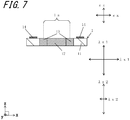
- the third substrate 13 has a quadrangular shape, and, in the plan view, the third substrate 13 extends more than the second substrate 12 in the longitudinal direction of the third substrate 13.
- heat transmitted from the second substrate 12 to the third substrate 13 can be transmitted more smoothly toward the outside of the electronic element mounting substrate 1, and also heat propagating in the vicinity of the corners of the second substrate 12 contacted by the third substrate 13 can be smoothly transmitted, through the third substrate 13, to a predetermined region. This makes it possible to render the electronic element mounting substrate 1 highly reliable.
- the third substrate 13 may be configured so that its ends extend beyond the ends of the second substrate 12 in the longitudinal direction of the third substrate 13, and more specifically, that one of the ends of the third substrate 13 which points in a positive direction along an imaginary y axis or that one of the ends thereof which points in a negative direction along the imaginary y axis extends beyond the corresponding end of the second substrate 12 in the longitudinal direction of the third substrate 13.
- the second substrate 12 exhibits higher thermal conductivity in the thickness direction thereof than in the longitudinal direction of the third substrate 13, whereas the third substrate 13 exhibits higher thermal conductivity in the longitudinal direction thereof than in a direction perpendicular to the longitudinal direction.
- the second substrate 12 and the third substrate 13 includes mutually opposing faces. During the operation of the electronic element 2 mounted on the second substrate 12, even if heat is transmitted through the entire area of the face of the second substrate 12 opposed to the face of the third substrate 13, the heat can be smoothly transmitted along the outer edge of the second substrate 12 in a direction perpendicular to the direction in which the second substrate 12 is disposed adjacent to the third substrate 13.
- the heat propagating in the direction in which the second substrate 12 is disposed adjacent to the third substrate 13 can be smoothly transmitted to a predetermined surrounding region opposed to the second substrate 12, and can be then smoothly transmitted to a predetermined region (e.g. a portion for external heat dissipation). Consequently, the electronic element mounting substrate 1 can become highly reliable.
- the electronic element mounting substrate 1 is capable of proper dissipation of heat from the light-emitting element mounted on the mounting portion 1a of the second substrate 12, ensuring satisfactory light emission from the light-emitting element.
- the first substrate 11 is shaped in a quadrangular frame, and is provided with the through hole 11a for embedding the second substrate 12 and the third substrate 13.
- the second substrate 12 is quadrangular in plan configuration.
- the third substrate 13 is quadrangular in plan configuration.
- the third substrate 13 extends more than the second substrate 12 in the longitudinal direction of the third substrate 13. That is, a length L2 of the third substrate 13 is greater than a length L1 of the second substrate 12 (L2 > L1).
- the first substrate 11, the second substrate 12, and the third substrate 13 are bonded together into a quadrangular composite substrate.
- the first substrate 11 is shaped in a square frame, and the second substrate 12 and the third substrate 13 each have a rectangular shape.
- the resulting composite substrate has a square form.
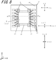
- the length L2 of the third substrate 13 in the longitudinal direction thereof is greater than a length L3 of a region where a plurality of metallic layers 14, etc. are arranged along the longitudinal direction of the third substrate 13 (L2 > L3).
- the heat transmitted from the second substrate 12 to the third substrate 13 is transmitted to the outside region beyond the region of the arrangement of the metallic layers 14, etc. This can facilitate transmission of heat to a predetermined region through the third substrate 13 while restraining heat transmission toward the region of the arrangement of a plurality of the metallic layers 14, etc. Consequently, the electronic element mounting substrate 1 can become highly reliable.
- each area of the third substrate 13 which protrudes in the longitudinal direction thereof protrudes outward beyond corresponding one of the ends of the region where the plurality of metallic layers 14, etc. are arranged near the second substrate 12. This can facilitate transmission of heat to a predetermined region through the third substrate 13 while restraining heat transmission toward the region of the arrangement of a plurality of the metallic layers 14, etc. Consequently, the electronic element mounting substrate 1 can become highly reliable.
- the electronic element mounting substrate 1 according to the second embodiment can be manufactured by a similar method to the method of manufacturing the electronic element mounting substrate 1 according to the preceding embodiment.
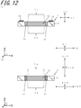
- the electronic element mounting substrate 1 according to the third embodiment of the disclosure differs from the electronic element mounting substrate 1 according to the preceding embodiment in that it includes a second mounting portion 1b for mounting a second electronic element 3, the second mounting portion 1b being located on a second principal face side in the thickness direction, and that, in the plan view, heat conduction of the second substrate 12 is higher in the planar direction thereof than in the thickness direction thereof.
- the third substrate 13 built in the form of a frame is disposed between the second substrate 12 and the third substrate 13.
- the third substrate 13 in frame form surrounds the second substrate 12.
- two third substrates 13 arranged facing each other in an imaginary x-axis direction have a thermal conductivity ⁇ 2
- two other third substrates 13 arranged facing each other in an imaginary y-axis direction have a thermal conductivity ⁇ 3.
- the thermal conductivity ⁇ 3 of the third substrate 13 in the x direction and the thermal conductivity ⁇ 3 thereof in the y direction differ in level from each other.
- the relationship among the thermal conductivities ⁇ 3 of the third substrate 13 in different directions, namely the relationship among ⁇ x3, ⁇ y3, and ⁇ z3 is expressed as: "thermal conductivity ⁇ x3 ⁇ thermal conductivity ⁇ z3 >> thermal conductivity ⁇ y2". That is, in the third substrate 13, the thermal conductivity ⁇ 3 in the x direction corresponding to the planar direction and the thermal conductivity ⁇ 3 in the z direction corresponding to the thickness direction are approximately equal, but the thermal conductivity ⁇ 3 in the y direction corresponding to the planar direction is different.
- the thermal conductivity ⁇ x3 and the thermal conductivity ⁇ z3 of the third substrate 13 are each about 1000 W/m ⁇ K, whereas the thermal conductivity ⁇ y3 of the third substrate 13 is about 4 W/m ⁇ K.
- one of the thermal conductivities ⁇ x3, ⁇ y3, and ⁇ z3 may be omitted for the sake of convenience.
- the second mounting portion 1b for mounting the second electronic element 3 is located on the second principal face side in the thickness direction, and heat conduction of the second substrate 12 is higher in the planar direction than in the thickness direction.
- the third substrate 13 is preferably configured so that the thermal conductivity in the extension direction of the side of the second substrate 12 is greater than the thermal conductivity in a direction perpendicular to the extention direction of the side of the second substrate 12.
- heat transmitted to the outer edge side of the second substrate 12 is smoothly dissipated while undergoing diffusion in the extension direction of the side of the second substrate 12, as well as in the thickness direction of the third substrate 13.
- the third substrate 13 may be shaped in a frame. In this case, in the plan view, the third substrate 13 surrounds the second substrate 12. Moreover, for example, four quadrangular third substrates 13 may be arranged in the form of a frame so as to surround the second substrate 12 in the plan view.
- the electronic element mounting substrate 1 according to the third embodiment can be manufactured by a similar method to the method of manufacturing the electronic element mounting substrate 1 according to the preceding embodiment.
- the electronic element mounting substrate 1 according to the fourth embodiment of the disclosure differs from the electronic element mounting substrate 1 according to the preceding embodiment in that the second substrates 12 and the third substrates 13 are arranged in a staggered format in the planar direction. Two second substrates 12 and two third substrates 13, or a total of four substrates are arranged in a 2- by 2-substrate matrix inside the first substrate 11.
- heat from the electronic element 2 can be distributively transmitted in different directions, namely the direction for the second substrate 12 to exhibit higher thermal conductivity ( ⁇ x1 direction) and the direction for the third substrate 13 to exhibit higher thermal conductivity ( ⁇ y2 direction). This makes it possible to impart high heat-conducting capability and high reliability to the electronic element mounting substrate 1.
- the mounting portion 1a is located so as to straddle the boundary between the second substrate 12 and the third substrate 13.
- heat from the electronic element 2 can be distributively transmitted in different directions, namely the direction for the second substrate 12 to exhibit higher thermal conductivity ( ⁇ x1 direction) and the direction for the third substrate 13 to exhibit higher thermal conductivity ( ⁇ y2 direction). This makes it possible to impart high heat-conducting capability and high reliability to the electronic element mounting substrate 1.
- the electronic element mounting substrate 1 according to the fourth embodiment can be manufactured by a similar method to the method of manufacturing the electronic element mounting substrate 1 according to the preceding embodiment.
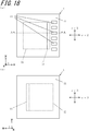
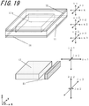
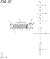
- the electronic element mounting substrate 1 according to the fifth embodiment of the disclosure differs from the electronic element mounting substrate 1 according to the preceding embodiment in that it includes a fourth substrate 15 and a fifth substrate 16.
- the fourth substrate 15 is disposed on the first principal face of the first substrate 11, and includes a seventh principal face (lower surface as viewed in FIGS. 18 to 22 ) opposed to the first principal face, and an eighth principal face (upper surface as viewed in FIGS. 18 to 22 ) located opposite to the seventh principal face.
- the fifth substrate 16 is disposed on the second principal face of the first substrate 11, and includes a ninth principal face (upper surface as viewed in FIGS. 18 to 22 ) opposed to the second principal face, and a tenth principal face (lower surface as viewed in FIGS. 18 to 22 ) located opposite to the ninth principal face.
- the outer surface of the first substrate 11, the outer surface of the fourth substrate 15, the outer surface of the fifth substrate 16, and the inner surface of the through hole 11a of the first substrate 11, which become invisible as viewed in perspective, are indicated by dotted lines.
- the illustrated second substrate 12 and third substrate 13 are each indicated by a dot-shaded area.
- the fourth substrate 15 and the fifth substrate 16 may be made of ceramics such as an aluminum oxide sintered body (alumina ceramics), an aluminum nitride sintered body, a mullite sintered body, and a glass ceramics sintered body.
- the fourth substrate 15 and the fifth substrate 16 may be produced by using the same material and method as those used for the production of the first substrate 11 made of ceramics as described above.
- an aluminum nitride sintered body which excels in thermal conductivity for the fourth substrate 15 and the fifth substrate 16.
- first substrate 11 is made of an aluminum nitride sintered body
- an aluminum nitride sintered body may be used for the fourth substrate 15 and the fifth substrate 16.
- the eighth principal face of the fourth substrate 15 is bonded with the first principal face of the first substrate 11, the third principal face of the second substrate 12, and the fifth principal face of the third substrate 13, via a joining material made of an active brazing filler metal, e.g. a Ti-Cu-Ag alloy or a Ti-Sn-Ag-Cu alloy.
- the ninth principal face of the fifth substrate 16 is bonded with the second principal face of the first substrate 11, the fourth principal face of the second substrate 12, and the sixth principal face of the third substrate 13, via a joining material made of an active brazing filler metal, e.g. a Ti-Cu-Ag alloy or a Ti-Sn-Ag-Cu alloy.
- the joining material which is about 10 ⁇ m thick, is interposed between the fourth substrate 15 and each of the first substrate 11, the second substrate 12, and the third substrate 13, or between the fifth substrate 16 and each of the first substrate 11, the second substrate 12, and the third substrate 13.
- a thermal conductivity ⁇ 2 of the fourth substrate 15 in the x direction and a thermal conductivity ⁇ 2 thereof in the y direction are substantially uniform.
- a thermal conductivity ⁇ 2 of the fourth substrate 15 in the z direction is approximately equal to the thermal conductivity ⁇ 2 in the planar direction, i.e. the x direction and the y direction ( ⁇ x2 ⁇ ⁇ y2 ⁇ ⁇ z2).
- the fourth substrate 15 is constructed of a substrate having a thermal conductivity ⁇ 2 of about 100 to 200 W/m ⁇ K.
- a thermal conductivity ⁇ 3 of the fifth substrate 16 in the x direction and a thermal conductivity ⁇ 3 thereof in the y direction are substantially uniform.
- a thermal conductivity ⁇ 3 of the fifth substrate 16 in the z direction is approximately equal to the thermal conductivity ⁇ 3 in the planar direction, i.e. the x direction and the y direction ( ⁇ x3 ⁇ ⁇ y3 ⁇ ⁇ z3).
- the fifth substrate 16 is constructed of a substrate having a thermal conductivity ⁇ 3 of about 100 to 200 W/m-K.
- one of the thermal conductivities ⁇ x2, ⁇ y2, ⁇ z2, ⁇ x3, ⁇ y3, and ⁇ z3 may be omitted for the sake of convenience.
- a metal material e.g. copper (Cu), copper-tungsten (Cu-W), and copper-molybdenum (Cu-Mo) may be used for the first substrate 11.
- the first substrate 11 is made of copper
- the first substrate 11 is constructed of a substrate having a thermal conductivity ⁇ of about 400 W/m-K.
- a thickness T4 of the fourth substrate 15 is about 50 ⁇ m to 500 ⁇ m.
- the second substrate 12 and the fourth substrate 15 fulfill the relationship in thickness given by: T2 > T4, and also the third substrate 13 and the fourth substrate 15 fulfill the relationship in thickness given by: T3 > T4. This permits satisfactory dissipation of heat from the electronic element 2 to the second substrate 12 and the third substrate 13 through the fourth substrate 15.
- a thickness T5 of the fifth substrate 16 falls in the range of about 50 ⁇ m to 500 ⁇ m.
- the thickness T4 of the fourth substrate 15 and the thickness T5 of the fifth substrate 16 are substantially equal, with an allowable margin between them limited to about 10% (0.90T5 ⁇ T4 ⁇ 1.10T5). This makes it possible to restrain the electronic element mounting substrate 1 against warpage more effectively, and thereby facilitate satisfactory light emission.
- the thickness of the fourth substrate 15 is set at 100 ⁇ m
- the thickness of the fifth substrate 16 is preferably set at 100 ⁇ m (within the range of 90 ⁇ m to 110 ⁇ m).
- the first substrate 11 is shaped in a quadrangular frame, and is provided with the through hole 11a for embedding the second substrate 12 and the third substrate 13.
- the second substrate 12 is quadrangular in plan configuration.
- the third substrate 13 is quadrangular in plan configuration.
- the fourth substrate 15 is quadrangular in plan configuration.
- the fifth substrate 16 is quadrangular in plan configuration.
- the first substrate 11, the second substrate 12, the third substrate 13, the fourth substrate 15, and the fifth substrate 16 are bonded together into a quadrangular composite substrate.
- the first substrate 11 is shaped in a square frame, and the second substrate 12 and the third substrate 13 each have a rectangular shape, and the fourth substrate 15 and the fifth substrate 16 each have a square shape.
- the resulting composite substrate has a square form.
- the fifth substrate 16 may be shaped in a frame.
- the fourth substrate 15 may differ between its thickness T4 in the part located on the center side of the electronic element mounting substrate 1 and its thickness T4 in the part located on the outer periphery side of the electronic element mounting substrate 1. That is, in the plan view, a part of the fourth substrate 15 which overlaps with the second substrate 12 and a part of the fourth substrate 15 which overlaps with the first substrate 11 may differ in thickness from each other.
- the fourth substrate 15 is thicker at the part thereof which overlaps with the second substrate 12 than at the part thereof which overlaps with the first substrate 11. This can facilitate more satisfactory dissipation of heat from the electronic element 2 mounted on the fourth substrate 15 toward the second substrate 12.
- the fifth substrate 16 may differ between its thickness T5 in the part located on the center side of the electronic element mounting substrate 1 and its thickness T5 in the part located on the outer periphery side of the electronic element mounting substrate 1. That is, in the plan view, a part of the fifth substrate 16 which overlaps with the second substrate 12 and a part of the fifth substrate 16 which overlaps with the first substrate 11 may differ in thickness from each other.
- the electronic element mounting substrate 1 according to the fifth embodiment can be manufactured by a similar method to the method of manufacturing the electronic element mounting substrate 1 according to the preceding embodiment.
- each of the electronic element mounting substrates 1 according to the first to fifth embodiments may be made in the form of a quadrangular composite substrate having beveled or chamfered corners.
- the electronic element mounting substrate 1 according to the disclosure may be implemented via a combination of the designs of some of the electronic element mounting substrates 1 according to the first to fifth embodiments. That is, for example, like the electronic element mounting substrate 1 according to the fifth embodiment, each of the electronic element mounting substrate 1 according to the second embodiment, the electronic element mounting substrate 1 according to the third embodiment, and the electronic element mounting substrate 1 according to the fourth embodiment may be provided with the fourth substrate 15 and the fifth substrate 16.
- the fifth substrate 16 may be located between the second substrate 12 and the third substrate 13 at the three sides of the third substrate 16.
- a mounting layer for the electronic element 2 may be disposed on the mounting portion 1a.
- the above-described mounting layer may be produced by using the same material and method as those used for the production of the metallic layer 14.
- the surfaces of the second substrate 12 and the third substrate 13 may be provided with, for example, a metallic plating layer including a Au plating layer located outermost.
Landscapes
- Engineering & Computer Science (AREA)
- Microelectronics & Electronic Packaging (AREA)
- Chemical & Material Sciences (AREA)
- Ceramic Engineering (AREA)
- Inorganic Chemistry (AREA)
- Structure Of Printed Boards (AREA)
- Cooling Or The Like Of Semiconductors Or Solid State Devices (AREA)
- Combinations Of Printed Boards (AREA)
- Physics & Mathematics (AREA)
- Geometry (AREA)
Abstract
Description
- The present invention relates to an electronic element mounting substrate, an electronic device, and an electronic module.
- In the related art, an electronic element mounting substrate includes: an insulating substrate including a first principal face, a second principal face, and side faces; and an electronic element mounting portion and a metallic layer located on each of the first principal face and the second principal face of the insulating substrate. In the electronic element mounting substrate, an electronic element is mounted on the electronic element mounting portion. Thus, an electronic device is constructed (refer to Japanese Unexamined Patent Publication
JP-A 2013-175508 - An electronic element mounting substrate according to the present disclosure includes: a first substrate including a first principal face and a second principal face located opposite to the first principal face; a second substrate located inside the first substrate in a plan view of the electronic element mounting substrate, the second substrate including a third principal face located on a first principal face side in a thickness direction of the electronic element mounting substrate and a fourth principal face located opposite to the third principal face, the second substrate being made of a carbon material; a third substrate located between the first substrate and the second substrate in the plan view of the electronic element mounting substrate, the third substrate including a fifth principal face located on the first principal face side in the thickness direction of the electronic element mounting substrate and a sixth principal face located opposite to the fifth principal face, the third substrate being made of a carbon material; and a first mounting portion for mounting a first electronic element, the first mounting portion being located on the first principal face side in the thickness direction of the electronic element mounting substrate, wherein the second substrate and the third substrate each have a low heat conduction direction in which heat conduction is low and a high heat conduction direction in which heat conduction is high, and the second substrate and the third substrate are arranged so that the low heat conduction directions of the second substrate and the third substrate are perpendicular to each other, and the high heat conduction directions of the second substrate and the third substrate are perpendicular to each other.
- An electronic device according to the disclosure includes: the electronic element mounting substrate mentioned above; and a first electronic element which is mounted on the first mounting portion of the electronic element mounting substrate.
- An electronic module according to the disclosure includes: the electronic device mentioned above; and a module substrate to which the electronic device is connected.
-
-
FIG. 1(a) is a top view showing an electronic element mounting substrate according to a first embodiment, andFIG. 1(b) is a bottom view of the substrate shown inFIG. 1(a) ; -
FIG. 2 is an exploded perspective view showing a first substrate, a second substrate, and a third substrate of the electronic element mounting substrate shown inFIG. 1 in a disassembled state; -
FIG. 3 is a vertical sectional view of the electronic element mounting substrate taken along the line A-A shown inFIG. 1(a) ; -
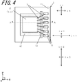
FIG. 4 is a top view showing the electronic element mounting substrate shown inFIG. 1 on which an electronic element is mounted; -
FIG. 5(a) is a top view showing an electronic element mounting substrate according to a second embodiment, andFIG. 5(b) is a bottom view of the substrate shown inFIG. 5(a) ; -
FIG. 6 is an exploded perspective view showing a first substrate, a second substrate, and a third substrate of the electronic element mounting substrate shown inFIG. 5 in a disassembled state; -
FIG. 7 is a vertical sectional view of the electronic element mounting substrate taken along the line A-A shown inFIG. 5(a) ; -
FIG. 8 is a top view showing the electronic element mounting substrate shown inFIG. 5 on which an electronic element is mounted; -
FIG. 9 is a vertical sectional view of the electronic element mounting substrate on which an electronic element is mounted taken along the line A-A shown inFIG. 8 ; -
FIG. 10(a) is a top view showing an electronic element mounting substrate according to a third embodiment, andFIG. 10(b) is a bottom view of the substrate shown inFIG. 10(a) ; -
FIG. 11 is an exploded perspective view showing a first substrate, a second substrate, and a third substrate of the electronic element mounting substrate shown inFIG. 10 in a disassembled state; -
FIG. 12(a) is a vertical sectional view of the electronic element mounting substrate taken along the line A-A shown inFIG. 10(a) , andFIG. 12(b) is a vertical sectional view of the electronic element mounting substrate taken along the line B-B shown inFIG. 10(a) ; -
FIG. 13(a) is a top view showing an electronic element mounting substrate according to a fourth embodiment, andFIG. 13(b) is a bottom view of the substrate shown inFIG. 13(a) ; -
FIG. 14 is an exploded perspective view showing a first substrate, a second substrate, and a third substrate of the electronic element mounting substrate shown inFIG. 13 in a disassembled state; -
FIG. 15(a) is a vertical sectional view of the electronic element mounting substrate taken along the line A-A shown inFIG. 13(a) , andFIG. 15(b) is a vertical sectional view of the electronic element mounting substrate taken along the line B-B shown inFIG. 13(a) ; -
FIG. 16 is a top view showing the electronic element mounting substrate shown inFIG. 13 on which an electronic element is mounted; -
FIG. 17(a) is a vertical sectional view of the electronic element mounting substrate on which the electronic element is mounted taken along the line A-A shown inFIG. 16 , andFIG. 17(b) is a vertical sectional view of the electronic element mounting substrate on which the electronic element is mounted taken along the line B-B shown inFIG. 16 ; -
FIG. 18(a) is a top view showing an electronic element mounting substrate according to a fifth embodiment, andFIG. 18(b) is a bottom view of the substrate shown inFIG. 18(a) ; -
FIG. 19 is an exploded perspective view showing a first substrate, a fourth substrate, a fifth substrate, a second substrate, and a third substrate of the electronic element mounting substrate shown inFIG. 18 in a disassembled state; -
FIG. 20 is a vertical sectional view of the electronic element mounting substrate taken along the line A-A shown inFIG. 18(a) ; -
FIG. 21 is a top view showing the electronic element mounting substrate shown inFIG. 18 on which an electronic element is mounted; and -
FIG. 22 is a vertical sectional view of the electronic device taken along the line A-A shown inFIG. 21 . - Several exemplary embodiments of the disclosure will now be described with reference to the accompanying drawings.
- As illustrated in
FIGS. 1 to 4 , an electronicelement mounting substrate 1 according to a first embodiment of the disclosure includes afirst substrate 11, asecond substrate 12, and athird substrate 13. An electronic device includes the electronicelement mounting substrate 1, an electronic element 2 (which may also be referred to as "firstelectronic element 2") mounted on a mounting portion 1a (which may also be referred to as "first mounting portion 1a") of the electronicelement mounting substrate 1, and a wiring substrate in which the electronicelement mounting substrate 1 is installed. For example, the electronic device is connected via a joining material to a connection pad disposed on a module substrate constituting an electronic module. - The electronic
element mounting substrate 1 according to this embodiment includes: thefirst substrate 11 including a first principal face and a second principal face located opposite to the first principal face; thesecond substrate 12 located inside thefirst substrate 11 in the plan view, thesecond substrate 12 including a third principal face located on the first principal face side in the thickness direction and a fourth principal face located opposite to the third principal face, thesecond substrate 12 being made of a carbon material; thethird substrate 13 located between thefirst substrate 11 and thesecond substrate 12 in the plan view, thethird substrate 13 including a fifth principal face located on the first principal face side in the thickness direction and a sixth principal face located opposite to the fifth principal face, thethird substrate 13 being made of a carbon material; and the mounting portion 1a for mounting an electronic element the mounting portion 1a being located on the first principal face. Thesecond substrate 12 and thethird substrate 13 each have a low heat conduction direction in which heat conduction is low and a high heat conduction direction in which heat conduction is high. Thesecond substrate 12 and thethird substrate 13 are arranged so that the low heat conduction directions of thesecond substrate 12 and thethird substrate 13 are perpendicular to each other, and also the high heat conduction directions of the second substrate and the third substrate are perpendicular to each other. InFIGS. 1 to 4 , theelectronic element 2 is shown as mounted on an xy plane in an imaginary xyz space. InFIGS. 1 to 4 , an upward direction conforms to a positive direction along an imaginary z axis. In the following description, the terms "upper" and "lower" are used as a matter of convenience and are not intended to be limiting of the oriented positions of the electronicelement mounting substrate 1, etc. in a vertical direction in terms of actual usage. - In
FIG. 2 , in the illustratedfirst substrate 11, the outer surface of thefirst substrate 11 and the inner surface of a through hole 11a of thefirst substrate 11, which become invisible as viewed in perspective, are indicated by dotted lines. InFIGS. 1 ,2 , and4 , the illustratedsecond substrate 12 andthird substrate 13 are each indicated by a dot-shaded area. - The
first substrate 11 includes the first principal face (upper surface as viewed inFIGS. 1 to 4 ) and the second principal face (lower surface as viewed inFIGS. 1 to 4 ). The first principal face and the second principal face are located opposite to each other. Thefirst substrate 11, including a single or a plurality of insulating layers, is shaped in a quadrangular plate including two pairs of opposite sides (four sides in total) positioned in relation to each of the first principal face and the second principal face in the plan view. Thefirst substrate 11 is provided with the through hole 11a formed so as to pass through between the first principal face and the second principal face thereof. The through hole 11a is polygonal, e.g. quadrangular, or circular in plan configuration. Thefirst substrate 11 serves also as a support for supporting thesecond substrate 12, thethird substrate 13, and theelectronic element 2. - For example, the
first substrate 11 may be made of ceramics such as an aluminum oxide sintered body (alumina ceramics), an aluminum nitride sintered body, a mullite sintered body, and a glass ceramics sintered body. For example, in the case where an aluminum nitride sintered body is used for thefirst substrate 11, a way to produce thefirst substrate 11 including a single or a plurality of insulating layers is as follows. A slurry is prepared first by admixing suitable organic binder, solvent, etc. in raw material powder such as aluminum nitride (AlN), erbium oxide (Er2O3), yttrium oxide (Y2O3), etc. The resulting slurry is shaped into a sheet by using heretofore known means such as a doctor blade method or a calender roll method, thereby forming a ceramic green sheet. On an as needed basis, a plurality of ceramic green sheets are stacked into a laminate. The ceramic green sheet or the laminate is fired at a high temperature (about 1800°C). - The
second substrate 12 includes the third principal face (upper surface as viewed inFIGS. 1 to 4 ) and the fourth principal face (lower surface as viewed inFIGS. 1 to 4 ). The third principal face and the fourth principal face are located opposite to each other. - The
third substrate 13 includes the fifth principal face (upper surface as viewed inFIGS. 1 to 4 ) and the sixth principal face (lower surface as viewed inFIGS. 1 to 4 ). The fifth principal face and the sixth principal face are located opposite to each other. - As illustrated in
FIGS. 1 to 4 , thesecond substrate 12 and thethird substrate 13 are embedded in thefirst substrate 11. Thesecond substrate 12 and thethird substrate 13 are disposed adjacent to each other in the plan view. That is, as illustrated inFIGS. 1 to 4 , thethird substrate 13 is located between thefirst substrate 11 and thesecond substrate 12 in the plan view. - For example, the
second substrate 12 and thethird substrate 13 are each made of a carbon material in the form of a graphene laminate structure containing six-membered rings joined together by covalent bonds, in which lamination planes are bound together by van der Waals' forces. - A
metallic layer 14 is disposed on the first principal face of thefirst substrate 11. Themetallic layer 14 is used as a connection portion for a connectingmember 3 such as a bonding wire, and serves to electrically connect theelectronic element 2 and a connection pad of a module substrate. - The
metallic layer 14 includes a thin-film layer and a plating layer. For example, the thin-film layer includes a metallic adherent layer and a barrier layer. The metallic adherent layer constituting the thin-film layer is formed on the first principal face of thefirst substrate 11. Examples of the material for the metallic adherent layer include tantalum nitride, a nickel-chromium material, a nickel-chromium-silicon material, a tungsten-silicon material, a molybdenum-silicon material, tungsten, molybdenum, titanium, and chromium. The metallic adherent layer is deposited on the first principal face of thefirst substrate 11 or an eighth principal face of afourth substrate 15 by using a thin-film forming technique such as vapor deposition, ion plating, or sputtering. For example, in the case where vacuum vapor deposition is adopted, a way to form the metallic adherent layer is as follows. Thefirst substrate 11 or thefourth substrate 15 is set in a film-forming chamber of a vacuum evaporator, and a metal piece for forming the metallic adherent layer is placed at an evaporation source within the film-forming chamber. After that, with the interior of the film-forming chamber maintained under vacuum (under a pressure of 10-2 Pa or below), the metal piece placed at the evaporation source is evaporated under heat, ensuring that the molecules of the described evaporated metal piece are deposited onto thefirst substrate 11, thereby forming a layer of a thin metallic film for forming the metallic adherent layer. Thefirst substrate 11 provided with the thin metallic film layer is subjected to a resist pattern-forming process using photolithography, and then an excess of the thin metallic film layer is removed by etching. Thus, the metallic adherent layer is obtained. A barrier layer is deposited on an upper surface of the metallic adherent layer. The barrier layer exhibits good adherability and wettability to the metallic adherent layer and the plating layer, and thus serves to join the metallic adherent layer with the plating layer firmly, as well as to prevent mutual diffusion of the metallic adherent layer and the plating layer. For example, the barrier layer is made of a nickel-chromium material, platinum, palladium, nickel, or cobalt. The barrier layer is deposited on the surface of the metallic adherent layer by using a thin-film forming technique such as vapor deposition, ion plating, or sputtering. - Preferably a thickness of the metallic adherent layer is about 0.01 µm to 0.5 µm. The thickness of less than 0.01 µm often results in difficulties in firm adhesion of the metallic adherent layer onto the
first substrate 11. The thickness of more than 0.5 µm often results in separation of the metallic adherent layer due to an internal stress developed in the metallic adherent layer-forming process. Moreover, preferably a thickness of the barrier layer is about 0.05 µm to 1 µm. The thickness of less than 0.05 µm often results in occurrence of defects such as pinholes, which may impair barrier layer's performance. The thickness of more than 1 µm often results in accidental separation of the barrier layer due to an internal stress developed in the barrier layer-forming process. - The plating layer is deposited on the exposed surface of the thin-film layer by using electrolytic plating or electroless plating. The plating layer is made of metal which is highly resistant to corrosion and affords high connectability to the connecting member, e.g. nickel, copper, gold, or silver. For example, the exposed surface is deposited successively with a nickel plating layer measuring about 0.5 µm to 5 µm in thickness and a gold plating layer measuring about 0.1 µm to 3 µm in thickness. This can retard corrosion of the
metallic layer 14 effectively, and also can strengthen the connection between themetallic layer 14 and the connectingmember 3. - Moreover, a metallic layer. such as copper (Cu) or gold (Au) may be placed on the barrier layer in the interest of successful formation of the plating layer. The above-described metallic layer is formed in a similar manner to that for forming the thin-film layer.
- It is preferred to use an aluminum nitride sintered body which excels in thermal conductivity for the
first substrate 1. The joining together of thefirst substrate 11 and thesecond substrate 12 is accomplished by bonding the outer surface of thesecond substrate 12 to the inner surface of the through hole 11a of thefirst substrate 11 via a joining material made of an active brazing filler metal, e.g. a Ti-Cu-Ag alloy or a Ti-Sn-Ag-Cu alloy. The joining together of thefirst substrate 11 and thethird substrate 13 is accomplished by bonding the outer surface of thethird substrate 13 to the inner surface of the through hole 11a of thefirst substrate 11 via a joining material made of an active brazing filler metal, e.g. a Ti-Cu-Ag alloy or a Ti-Sn-Ag-Cu alloy. The joining material, which is about 10 µm thick, is interposed between thefirst substrate 11 and thesecond substrate 12, or between thefirst substrate 11 and thethird substrate 13. - In the plan view, the
first substrate 11 is shaped in a quadrangular frame, and is provided with the through hole 11a for embedding thesecond substrate 12 and thethird substrate 13. Thesecond substrate 12 is quadrangular in plan configuration. Thethird substrate 13 is quadrangular in plan configuration. Thefirst substrate 11, thesecond substrate 12, and thethird substrate 13 are bonded together into a quadrangular composite substrate. As used herein the term "quadrangular configuration" means the shape of a quadrilateral such as a square and a rectangle. In the plan view, thefirst substrate 11 is shaped in a square frame, and, thesecond substrate 12 and thethird substrate 13 each have a rectangular shape. Thus, the resulting composite substrate has a square form. - For example, a thickness T1 of the
first substrate 11 T1 is about 100 µm to 2000 µm, and a thickness T2 of thesecond substrate 12 is about 100 µm to 2000 µm. For example, a thickness T3 of thethird substrate 13 is about 100 µm to 2000 µm. That is, the thickness T1 of thefirst substrate 11 and the thickness T2 of thesecond substrate 12 are substantially equal (0.9T1 ≤ T2 ≤ 1.1T1). Also, the thickness T1 of thefirst substrate 11 and the thickness T3 of thethird substrate 13 are substantially equal (0.9T1 ≤ T3 ≤ 1.1T1). - Following the production of the composite substrate including the
first substrate 11, thesecond substrate 12, and thethird substrate 13 joined together via the joining material, themetallic layer 14 is formed on the first principal face of thefirst substrate 11. Thus, the electronicelement mounting substrate 1 is constructed. - In the planar direction of the
first substrate 11, a thermal conductivity κ of thefirst substrate 11 in an x direction and a thermal conductivity κ thereof in a y direction are substantially uniform. Moreover, in the thickness direction of thefirst substrate 11, a thermal conductivity κ of thefirst substrate 11 in a z direction is approximately equal to the thermal conductivity κ in the planar direction, i.e. the x direction and the y direction (κx ≈ κy ≈ κz). For example, in the case where an aluminum nitride sintered body is used for thefirst substrate 11, thefirst substrate 11 is constructed of a substrate having a thermal conductivity κ of about 100 to 200 W/m-K. - In the planar direction of the
second substrate 12, a thermal conductivity λ1 of thesecond substrate 12 in the x direction and a thermal conductivity λ1 thereof in the y direction differ in level from each other. That is, in thesecond substrate 12, the thermal conductivity λ in the x direction corresponding to the planar direction and the thermal conductivity λ in the z direction corresponding to the thickness direction are approximately equal, but the thermal conductivity λ in the y direction corresponding to the planar direction is different. The relationship among the thermal conductivities λ1 of thesecond substrate 12 in different directions, namely the relationship among λx1, λy1, and λz1 is expressed as: "thermal conductivity λx1 ≈ thermal conductivity λz1 >> thermal conductivity λy1". For example, the thermal conductivity λx1 and the thermal conductivity λz1 of thesecond substrate 12 are each about 1000 W/m-K, whereas the thermal conductivity λy1 of thesecond substrate 12 is about 4 W/m·K. - In the planar direction of the
third substrate 13, a thermal conductivity λ2 of thethird substrate 13 in the x direction and a thermal conductivity λ2 thereof in the y direction differ in level from each other. That is, in thethird substrate 13, the thermal conductivity λ in the y direction corresponding to the planar direction and the thermal conductivity λ in the z direction corresponding to the thickness direction are approximately equal, but the thermal conductivity λ in the x direction corresponding to the planar direction is different. The relationship among the thermal conductivities λ2 of thethird substrate 13 in different directions, namely the relationship among λx2, λy2, and λz2 is expressed as: "thermal conductivity λy2 ≈ thermal conductivity λz2 >> thermal conductivity λx2". For example, the thermal conductivity λy2 and the thermal conductivity λz2 of thethird substrate 13 are each about 1000 W/m·K, whereas the thermal conductivity λx1 of thethird substrate 13 is about 4 W/m·K. That is, the direction for thesecond substrate 12 to exhibit a higher (lower) thermal conductivity λ1 differs from the direction for thethird substrate 13 to exhibit a higher (lower) thermal conductivity λ2. In some drawings for this embodiment, as well as in some drawings for embodiments that will hereinafter be described, one of the thermal conductivities κx, κy, κz, λx1, λy1, λz1, λx2, λy2, and λz2 may be omitted for the sake of convenience. - The electronic device can be produced by mounting the
electronic element 2 on the mounting portion 1a of thesecond substrate 12 of the electronicelement mounting substrate 1. It is also satisfactory to produce the electronic device by installing the electronicelement mounting substrate 1 on which theelectronic element 2 is mounted, in a wiring substrate or electronic element mounting package. Examples of theelectronic element 2 mounted on the electronicelement mounting substrate 1 include light-emitting elements such as LD (Laser Diode) and LED (Light Emitting Diode) and light-receiving elements such as PD (Photo Diode). For example, theelectronic element 2 is fixedly disposed on the mounting portion 1a of thesecond substrate 12 via a joining material such as a Au-Sn material. After that, an electrode of theelectronic element 2 is electrically connected to themetallic layer 14 via the connectingmember 3 such as a bonding wire. Thus, the mounting of theelectronic element 2 on the electronicelement mounting substrate 1 is accomplished. If using a wiring substrate or electronic element mounting package in which the electronicelement mounting substrate 1 is installed, the wiring substrate or electronic element mounting package may be, like thefirst substrate 11, constructed of an insulating base body made of ceramics or the like including a wiring conductor on a surface thereof. Moreover, if using a wiring substrate or electronic element mounting package in which the electronicelement mounting substrate 1 is installed, themetallic layer 14 of the electronicelement mounting substrate 1 is electrically connected to the wiring conductor of the wiring substrate or electronic element mounting package. - The electronic
element mounting substrate 1 according to this embodiment includes: thefirst substrate 11 including the first principal face and the second principal face located opposite to the first principal face; thesecond substrate 12 located inside thefirst substrate 11 in the plan view, thesecond substrate 12 including the third principal face located on the first principal face side in the thickness direction and the fourth principal face located opposite to the third principal face, thesecond substrate 12 being made of a carbon material; thethird substrate 13 located between thefirst substrate 11 and thesecond substrate 12 in the plan view, thethird substrate 13 including the fifth principal face located on the first principal face side in the thickness direction and the sixth principal face located opposite to the fifth principal face,third substrate 13 being made of a carbon material; and the mounting portion 1a for mounting theelectronic element 2, the mounting portion 1a being located on the first principal face side in the thickness direction. Thesecond substrate 12 and thethird substrate 13 each have the low heat conduction direction and the high heat conduction direction. Thesecond substrate 12 and thethird substrate 13 are arranged so that the low heat conduction directions of thesecond substrate 12 and thethird substrate 13 are perpendicular to each other (λy1 direction ⊥ λx2 direction) and also the high heat conduction directions of thesecond substrate 12 and thethird substrate 13 are perpendicular to each other (λx1 direction ⊥ λy2 direction). With this arrangement, during the operation of theelectronic element 2 mounted on the mounting portion 1a, in the plan view, heat from theelectronic element 2 is distributively transmitted in different directions, namely the direction for thesecond substrate 12 to exhibit higher thermal conductivity (λx1 direction) and the direction for thethird substrate 13 to exhibit higher thermal conductivity (λy2 direction). This makes it possible to impart high heat-conducting capability and high reliability to the electronicelement mounting substrate 1. - Moreover, the
third substrate 13 has a quadrangular shape, and, in the plan view, heat conduction of thesecond substrate 12 is higher in a direction perpendicular to the longitudinal direction of thethird substrate 13 than in the longitudinal direction of thethird substrate 13, and heat conduction of thethird substrate 13 is higher in the longitudinal direction thereof than in a direction perpendicular to the longitudinal direction. This can facilitate, during the operation of theelectronic element 2 mounted on thesecond substrate 12, transmission of heat to the third substrate while restraining heat transmission to a region opposed to the side of thesecond substrate 12, and also restraining heat transmission in a direction perpendicular to the direction in which thesecond substrate 12 is disposed adjacent to thethird substrate 13. The heat transmitted to thethird substrate 13 side can be smoothly transmitted along the outer edge of thesecond substrate 12 in the direction perpendicular to the direction in which thesecond substrate 12 is disposed adjacent to thethird substrate 13. Thus, in the plan view, the heat propagating in the direction in which thesecond substrate 12 is disposed adjacent to thethird substrate 13 can be smoothly transmitted to a predetermined surrounding region opposed to thesecond substrate 12, and can be then smoothly transmitted to a predetermined region (e.g. a portion for external heat dissipation). Consequently, the electronicelement mounting substrate 1 can become highly reliable. - Moreover, as illustrated in
FIGS. 5 to 9 which will hereafter be referred to, preferably, in the plan view, thethird substrates 13 are arranged with thesecond substrate 12 in between. In this case, during the operation of theelectronic element 2 mounted on thesecond substrate 12 and thethird substrate 13, heat liberated by theelectronic element 2 on thethird substrate 13 can be smoothly transmitted in a direction perpendicular to the direction in which thethird substrates 13 are arranged with thesecond substrate 12 in between rather than in the direction in which the two opposed sides of theelectronic element 2 are located with thesecond substrate 12 in between. This makes it possible to restrain heat against propagation from the outer edge of theelectronic element 2 situated on thethird substrate 13 to the central area of theelectronic element 2, and thereby operate theelectronic element 2 effectively for long periods with little deterioration in performance. - The
second substrate 12 exhibits higher thermal conductivity in the direction of its thickness than in the longitudinal direction of thethird substrate 13, whereas thethird substrate 13 exhibits higher thermal conductivity in the longitudinal direction thereof than in a direction perpendicular to the longitudinal direction. Thesecond substrate 12 and thethird substrate 13 include mutually opposing faces. During the operation of theelectronic element 2 mounted on thesecond substrate 12, even if heat is transmitted through the entire area of the face of thesecond substrate 12 opposed to the face of thethird substrate 13, the heat can be smoothly transmitted along the outer edge of thesecond substrate 12 in a direction perpendicular to the direction in which thesecond substrate 12 is disposed adjacent to thethird substrate 13. Thus, in the plan view, the heat propagating in the direction in which thesecond substrate 12 is disposed adjacent to thethird substrate 13 can be smoothly transmitted to a predetermined surrounding region opposed to thesecond substrate 12, and can be then smoothly transmitted to a predetermined region (e.g. a portion for external heat dissipation). Consequently, the electronicelement mounting substrate 1 can become highly reliable. - Moreover, in the case where a light-emitting element is used as the
electronic element 2, the electronicelement mounting substrate 1 is capable of proper dissipation of heat from the light-emitting element mounted on the mounting portion 1a located on the first principal face side, ensuring satisfactory light emission from the light-emitting element. - The electronic device according to this embodiment includes the electronic
element mounting substrate 1 mentioned above and theelectronic element 2 mounted on the mounting portion 1a of the electronicelement mounting substrate 1. Thus constructed, the electronic device can remain reliable for long periods. - The electronic device according to this embodiment is connected, at the
metallic layer 14 of the electronicelement mounting substrate 1 thereof, to the connection pad of the module substrate via a joining material such as solder, thereby constituting the electronic module. Thus, theelectronic element 2 and the connection pad of the module substrate are electrically connected to each other. - Moreover, in the case where the electronic device includes a wiring substrate or electronic element housing package in which the electronic
element mounting substrate 1 is installed, the electronic device is connected, at the wiring conductor of the wiring substrate or electronic element housing package thereof, to the connection pad of the module substrate via a joining material such as solder, thereby constituting the electronic module. Thus, theelectronic element 2 and the connection pad of the module substrate are electrically connected to each other. - The electronic module according to this embodiment includes the electronic device mentioned above and the module substrate to which the electronic device is connected. Thus constructed, the electronic module can remain reliable for long periods.
- While the
metallic layer 14 disposed on the first principal face of thefirst substrate 11 is, as exemplified, formed by using a thin-film method, themetallic layer 14 may be formed by using heretofore known co-firing or post-firing . - The following describes an electronic device according to a second embodiment of the disclosure with reference to
FIGS. 5 to 9 andFIGS. 1 to 4 as well. - In the electronic
element mounting substrate 1 according to the second embodiment of the disclosure, in the plan view, thethird substrate 13 extends more than thesecond substrate 12 in the longitudinal direction of thethird substrate 13. This design holds true for the embodiment shown inFIGS. 1 to 4 . - In
FIG. 6 , in the illustratedfirst substrate 1, the outer surface of thefirst substrate 11 and the inner surface of the through hole 11a of thefirst substrate 11, which become invisible as viewed in perspective, are indicated by dotted lines. InFIGS. 5 ,6 , and8 , the illustratedsecond substrate 12 andthird substrate 13 are each indicated by a dot-shaded area. - Moreover, the
third substrate 13 has a quadrangular shape, and, in the plan view, thethird substrate 13 extends more than thesecond substrate 12 in the longitudinal direction of thethird substrate 13. In this case, heat transmitted from thesecond substrate 12 to thethird substrate 13 can be transmitted more smoothly toward the outside of the electronicelement mounting substrate 1, and also heat propagating in the vicinity of the corners of thesecond substrate 12 contacted by thethird substrate 13 can be smoothly transmitted, through thethird substrate 13, to a predetermined region. This makes it possible to render the electronicelement mounting substrate 1 highly reliable. Note that thethird substrate 13 may be configured so that its ends extend beyond the ends of thesecond substrate 12 in the longitudinal direction of thethird substrate 13, and more specifically, that one of the ends of thethird substrate 13 which points in a positive direction along an imaginary y axis or that one of the ends thereof which points in a negative direction along the imaginary y axis extends beyond the corresponding end of thesecond substrate 12 in the longitudinal direction of thethird substrate 13. - The
second substrate 12 exhibits higher thermal conductivity in the thickness direction thereof than in the longitudinal direction of thethird substrate 13, whereas thethird substrate 13 exhibits higher thermal conductivity in the longitudinal direction thereof than in a direction perpendicular to the longitudinal direction. Thesecond substrate 12 and thethird substrate 13 includes mutually opposing faces. During the operation of theelectronic element 2 mounted on thesecond substrate 12, even if heat is transmitted through the entire area of the face of thesecond substrate 12 opposed to the face of thethird substrate 13, the heat can be smoothly transmitted along the outer edge of thesecond substrate 12 in a direction perpendicular to the direction in which thesecond substrate 12 is disposed adjacent to thethird substrate 13. Thus, in the plan view, the heat propagating in the direction in which thesecond substrate 12 is disposed adjacent to thethird substrate 13 can be smoothly transmitted to a predetermined surrounding region opposed to thesecond substrate 12, and can be then smoothly transmitted to a predetermined region (e.g. a portion for external heat dissipation). Consequently, the electronicelement mounting substrate 1 can become highly reliable. - Moreover, in the case where a light-emitting element is used as the
electronic element 2, the electronicelement mounting substrate 1 is capable of proper dissipation of heat from the light-emitting element mounted on the mounting portion 1a of thesecond substrate 12, ensuring satisfactory light emission from the light-emitting element. - In the plan view, the
first substrate 11 is shaped in a quadrangular frame, and is provided with the through hole 11a for embedding thesecond substrate 12 and thethird substrate 13. Thesecond substrate 12 is quadrangular in plan configuration. Thethird substrate 13 is quadrangular in plan configuration. Thethird substrate 13 extends more than thesecond substrate 12 in the longitudinal direction of thethird substrate 13. That is, a length L2 of thethird substrate 13 is greater than a length L1 of the second substrate 12 (L2 > L1).
Thefirst substrate 11, thesecond substrate 12, and thethird substrate 13 are bonded together into a quadrangular composite substrate. In the plan view, thefirst substrate 11 is shaped in a square frame, and thesecond substrate 12 and thethird substrate 13 each have a rectangular shape. Thus, the resulting composite substrate has a square form. - Moreover, preferably, the length L2 of the
third substrate 13 in the longitudinal direction thereof is greater than a length L3 of a region where a plurality ofmetallic layers 14, etc. are arranged along the longitudinal direction of the third substrate 13 (L2 > L3). In this case, the heat transmitted from thesecond substrate 12 to thethird substrate 13 is transmitted to the outside region beyond the region of the arrangement of themetallic layers 14, etc. This can facilitate transmission of heat to a predetermined region through thethird substrate 13 while restraining heat transmission toward the region of the arrangement of a plurality of themetallic layers 14, etc. Consequently, the electronicelement mounting substrate 1 can become highly reliable. - Moreover, preferably, each area of the
third substrate 13 which protrudes in the longitudinal direction thereof protrudes outward beyond corresponding one of the ends of the region where the plurality ofmetallic layers 14, etc. are arranged near thesecond substrate 12. This can facilitate transmission of heat to a predetermined region through thethird substrate 13 while restraining heat transmission toward the region of the arrangement of a plurality of themetallic layers 14, etc. Consequently, the electronicelement mounting substrate 1 can become highly reliable. - Otherwise, the electronic
element mounting substrate 1 according to the second embodiment can be manufactured by a similar method to the method of manufacturing the electronicelement mounting substrate 1 according to the preceding embodiment. - The following describes an electronic device according to a third embodiment of the disclosure with reference to
FIGS. 10 to 12 . - The electronic
element mounting substrate 1 according to the third embodiment of the disclosure differs from the electronicelement mounting substrate 1 according to the preceding embodiment in that it includes a second mounting portion 1b for mounting a secondelectronic element 3, the second mounting portion 1b being located on a second principal face side in the thickness direction, and that, in the plan view, heat conduction of thesecond substrate 12 is higher in the planar direction thereof than in the thickness direction thereof. - In the electronic
element mounting substrate 1 according to the third embodiment, in the plan view, thethird substrate 13 built in the form of a frame is disposed between thesecond substrate 12 and thethird substrate 13. Thethird substrate 13 in frame form surrounds thesecond substrate 12. - In the electronic
element mounting substrate 1 according to the third embodiment, twothird substrates 13 arranged facing each other in an imaginary x-axis direction (indicated by light shaded areas inFIGS. 10 and11 ) have a thermal conductivity λ2, whereas two otherthird substrates 13 arranged facing each other in an imaginary y-axis direction (indicated by dark shaded areas inFIGS. 10 and11 ) have a thermal conductivity λ3. There are differences in the direction for thesecond substrate 12 to exhibit a higher (lower) thermal conductivity λ, the direction for thethird substrate 13 to exhibit a higher (lower) thermal conductivity λ2, and the direction for the otherthird substrate 13 to exhibit a higher (lower) thermal conductivity λ3. - In the planar direction of the
third substrate 13, the thermal conductivity λ3 of thethird substrate 13 in the x direction and the thermal conductivity λ3 thereof in the y direction differ in level from each other. The relationship among the thermal conductivities λ3 of thethird substrate 13 in different directions, namely the relationship among λx3, λy3, and λz3 is expressed as: "thermal conductivity λx3 ≈ thermal conductivity λz3 >> thermal conductivity λy2". That is, in thethird substrate 13, the thermal conductivity λ3 in the x direction corresponding to the planar direction and the thermal conductivity λ3 in the z direction corresponding to the thickness direction are approximately equal, but the thermal conductivity λ3 in the y direction corresponding to the planar direction is different. For example, the thermal conductivity λx3 and the thermal conductivity λz3 of thethird substrate 13 are each about 1000 W/m·K, whereas the thermal conductivity λy3 of thethird substrate 13 is about 4 W/m·K. In some drawings for this embodiment, as well as in some drawings for embodiments that will hereinafter be described, one of the thermal conductivities λx3, λy3, and λz3 may be omitted for the sake of convenience. - In this construction, the second mounting portion 1b for mounting the second
electronic element 3 is located on the second principal face side in the thickness direction, and heat conduction of thesecond substrate 12 is higher in the planar direction than in the thickness direction. Thus, during the operation of the firstelectronic element 2 mounted on the first mounting portion 1a and the secondelectronic element 3 mounted on the second mounting portion 1b, heat liberated by the firstelectronic element 2 and heat liberated by the secondelectronic element 3 are each transmitted smoothly in the planar direction from corresponding one of the first mounting portion 1a and the second mounting portion 1b located opposite each other toward the outer periphery of corresponding one of the first mounting portion 1a and the second mounting portion 1b. This makes it possible to reduce accumulation of heat at each of the first mounting portion 1a and the second mounting portion 1b, and thereby prevent impairment of the operational capability of the firstelectronic element 2 mounted on the first mounting portion 1a and the secondelectronic element 3 mounted on the second mounting portion 1b, ensuring good performance of the firstelectronic element 2 and the secondelectronic element 3. - Moreover, the
third substrate 13 is preferably configured so that the thermal conductivity in the extension direction of the side of thesecond substrate 12 is greater than the thermal conductivity in a direction perpendicular to the extention direction of the side of thesecond substrate 12. In this case, heat transmitted to the outer edge side of thesecond substrate 12 is smoothly dissipated while undergoing diffusion in the extension direction of the side of thesecond substrate 12, as well as in the thickness direction of thethird substrate 13. Thus, during the operation of the firstelectronic element 2 mounted on the first mounting portion 1a and the secondelectronic element 3 mounted on the second mounting portion 1b, heat can be properly released to the outside, in consequence whereof there results no impairment of the operational capability of the firstelectronic element 2 mounted on the first mounting portion 1a and the secondelectronic element 3 mounted on the second mounting portion 1b. This can ensure good performance of the firstelectronic element 2 and the secondelectronic element 3. Thethird substrate 13 may be shaped in a frame. In this case, in the plan view, thethird substrate 13 surrounds thesecond substrate 12. Moreover, for example, four quadrangularthird substrates 13 may be arranged in the form of a frame so as to surround thesecond substrate 12 in the plan view. - Otherwise, the electronic
element mounting substrate 1 according to the third embodiment can be manufactured by a similar method to the method of manufacturing the electronicelement mounting substrate 1 according to the preceding embodiment. - The following describes an electronic device according to a fourth embodiment of the disclosure with reference to
FIGS. 13 to 17 . - The electronic
element mounting substrate 1 according to the fourth embodiment of the disclosure differs from the electronicelement mounting substrate 1 according to the preceding embodiment in that thesecond substrates 12 and thethird substrates 13 are arranged in a staggered format in the planar direction. Twosecond substrates 12 and twothird substrates 13, or a total of four substrates are arranged in a 2- by 2-substrate matrix inside thefirst substrate 11. - With the staggered arrangement of the second and
third substrates electronic element 2 mounted on the mounting portion 1a, in the plan view, heat from theelectronic element 2 can be distributively transmitted in different directions, namely the direction for thesecond substrate 12 to exhibit higher thermal conductivity (λx1 direction) and the direction for thethird substrate 13 to exhibit higher thermal conductivity (λy2 direction). This makes it possible to impart high heat-conducting capability and high reliability to the electronicelement mounting substrate 1. - Moreover, in the plan view, the mounting portion 1a is located so as to straddle the boundary between the
second substrate 12 and thethird substrate 13. In this case, during the operation of theelectronic element 2 mounted on the mounting portion 1a, in the plan view, heat from theelectronic element 2 can be distributively transmitted in different directions, namely the direction for thesecond substrate 12 to exhibit higher thermal conductivity (λx1 direction) and the direction for thethird substrate 13 to exhibit higher thermal conductivity (λy2 direction). This makes it possible to impart high heat-conducting capability and high reliability to the electronicelement mounting substrate 1. - Otherwise, the electronic
element mounting substrate 1 according to the fourth embodiment can be manufactured by a similar method to the method of manufacturing the electronicelement mounting substrate 1 according to the preceding embodiment. - The following describes an electronic device according to a fifth embodiment of the disclosure with reference to
FIGS. 18 to 22 . - The electronic
element mounting substrate 1 according to the fifth embodiment of the disclosure differs from the electronicelement mounting substrate 1 according to the preceding embodiment in that it includes afourth substrate 15 and afifth substrate 16. Thefourth substrate 15 is disposed on the first principal face of thefirst substrate 11, and includes a seventh principal face (lower surface as viewed inFIGS. 18 to 22 ) opposed to the first principal face, and an eighth principal face (upper surface as viewed inFIGS. 18 to 22 ) located opposite to the seventh principal face. Thefifth substrate 16 is disposed on the second principal face of thefirst substrate 11, and includes a ninth principal face (upper surface as viewed inFIGS. 18 to 22 ) opposed to the second principal face, and a tenth principal face (lower surface as viewed inFIGS. 18 to 22 ) located opposite to the ninth principal face. - In
FIG. 19 , in the illustratedfirst substrate 11,fourth substrate 15, andfifth substrate 16, the outer surface of thefirst substrate 11, the outer surface of thefourth substrate 15, the outer surface of thefifth substrate 16, and the inner surface of the through hole 11a of thefirst substrate 11, which become invisible as viewed in perspective, are indicated by dotted lines. InFIG. 19 , the illustratedsecond substrate 12 andthird substrate 13 are each indicated by a dot-shaded area. - For example, the
fourth substrate 15 and thefifth substrate 16 may be made of ceramics such as an aluminum oxide sintered body (alumina ceramics), an aluminum nitride sintered body, a mullite sintered body, and a glass ceramics sintered body. Thefourth substrate 15 and thefifth substrate 16 may be produced by using the same material and method as those used for the production of thefirst substrate 11 made of ceramics as described above. - It is preferred to use an aluminum nitride sintered body which excels in thermal conductivity for the
fourth substrate 15 and thefifth substrate 16. In the case where thefirst substrate 11 is made of an aluminum nitride sintered body, an aluminum nitride sintered body may be used for thefourth substrate 15 and thefifth substrate 16. The eighth principal face of thefourth substrate 15 is bonded with the first principal face of thefirst substrate 11, the third principal face of thesecond substrate 12, and the fifth principal face of thethird substrate 13, via a joining material made of an active brazing filler metal, e.g. a Ti-Cu-Ag alloy or a Ti-Sn-Ag-Cu alloy. The ninth principal face of thefifth substrate 16 is bonded with the second principal face of thefirst substrate 11, the fourth principal face of thesecond substrate 12, and the sixth principal face of thethird substrate 13, via a joining material made of an active brazing filler metal, e.g. a Ti-Cu-Ag alloy or a Ti-Sn-Ag-Cu alloy. The joining material, which is about 10 µm thick, is interposed between thefourth substrate 15 and each of thefirst substrate 11, thesecond substrate 12, and thethird substrate 13, or between thefifth substrate 16 and each of thefirst substrate 11, thesecond substrate 12, and thethird substrate 13. - In the planar direction of the
fourth substrate 15, a thermal conductivity κ2 of thefourth substrate 15 in the x direction and a thermal conductivity κ2 thereof in the y direction are substantially uniform. Moreover, in the thickness direction of thefourth substrate 15, a thermal conductivity κ2 of thefourth substrate 15 in the z direction is approximately equal to the thermal conductivity κ2 in the planar direction, i.e. the x direction and the y direction (κx2 ≈ κy2 ≈ κz2). For example, where sintered aluminum nitride is used for thefourth substrate 15, thefourth substrate 15 is constructed of a substrate having a thermal conductivity κ2 of about 100 to 200 W/m·K. - In the planar direction of the
fifth substrate 16, a thermal conductivity κ3 of thefifth substrate 16 in the x direction and a thermal conductivity κ3 thereof in the y direction are substantially uniform. Moreover, in the thickness direction of thefifth substrate 16, a thermal conductivity κ3 of thefifth substrate 16 in the z direction is approximately equal to the thermal conductivity κ3 in the planar direction, i.e. the x direction and the y direction (κx3 ≈ κy3 ≈ κz3). For example, in the case where an aluminum nitride sintered body is used for thefifth substrate 16, thefifth substrate 16 is constructed of a substrate having a thermal conductivity κ3 of about 100 to 200 W/m-K. In some drawings for this embodiment, one of the thermal conductivities κx2, κy2, κz2, κx3, κy3, and κz3 may be omitted for the sake of convenience. - Moreover, in the electronic
element mounting substrate 1 according to the fifth embodiment, a metal material, e.g. copper (Cu), copper-tungsten (Cu-W), and copper-molybdenum (Cu-Mo) may be used for thefirst substrate 11. For example, where thefirst substrate 11 is made of copper, thefirst substrate 11 is constructed of a substrate having a thermal conductivity κ of about 400 W/m-K. - For example, a thickness T4 of the
fourth substrate 15 is about 50 µm to 500 µm. Preferably, thesecond substrate 12 and thefourth substrate 15 fulfill the relationship in thickness given by: T2 > T4, and also thethird substrate 13 and thefourth substrate 15 fulfill the relationship in thickness given by: T3 > T4. This permits satisfactory dissipation of heat from theelectronic element 2 to thesecond substrate 12 and thethird substrate 13 through thefourth substrate 15. - Moreover, a thickness T5 of the
fifth substrate 16, like the thickness T1 of thefirst substrate 11, falls in the range of about 50 µm to 500 µm. Preferably, the thickness T4 of thefourth substrate 15 and the thickness T5 of thefifth substrate 16 are substantially equal, with an allowable margin between them limited to about 10% (0.90T5 ≤ T4 ≤ 1.10T5). This makes it possible to restrain the electronicelement mounting substrate 1 against warpage more effectively, and thereby facilitate satisfactory light emission. For example, in the case where the thickness of thefourth substrate 15 is set at 100 µm, the thickness of thefifth substrate 16 is preferably set at 100 µm (within the range of 90 µm to 110 µm). - In the plan view, the
first substrate 11 is shaped in a quadrangular frame, and is provided with the through hole 11a for embedding thesecond substrate 12 and thethird substrate 13. Thesecond substrate 12 is quadrangular in plan configuration. Thethird substrate 13 is quadrangular in plan configuration. Thefourth substrate 15 is quadrangular in plan configuration. Thefifth substrate 16 is quadrangular in plan configuration. Thefirst substrate 11, thesecond substrate 12, thethird substrate 13, thefourth substrate 15, and thefifth substrate 16 are bonded together into a quadrangular composite substrate. In the plan view, thefirst substrate 11 is shaped in a square frame, and thesecond substrate 12 and thethird substrate 13 each have a rectangular shape, and thefourth substrate 15 and thefifth substrate 16 each have a square shape. Thus, the resulting composite substrate has a square form. - Moreover, in the electronic
element mounting substrate 1 according to the fifth embodiment, thefifth substrate 16 may be shaped in a frame. - Moreover, the
fourth substrate 15 may differ between its thickness T4 in the part located on the center side of the electronicelement mounting substrate 1 and its thickness T4 in the part located on the outer periphery side of the electronicelement mounting substrate 1. That is, in the plan view, a part of thefourth substrate 15 which overlaps with thesecond substrate 12 and a part of thefourth substrate 15 which overlaps with thefirst substrate 11 may differ in thickness from each other. Preferably, thefourth substrate 15 is thicker at the part thereof which overlaps with thesecond substrate 12 than at the part thereof which overlaps with thefirst substrate 11. This can facilitate more satisfactory dissipation of heat from theelectronic element 2 mounted on thefourth substrate 15 toward thesecond substrate 12. - Also, the
fifth substrate 16 may differ between its thickness T5 in the part located on the center side of the electronicelement mounting substrate 1 and its thickness T5 in the part located on the outer periphery side of the electronicelement mounting substrate 1. That is, in the plan view, a part of thefifth substrate 16 which overlaps with thesecond substrate 12 and a part of thefifth substrate 16 which overlaps with thefirst substrate 11 may differ in thickness from each other. - Otherwise, the electronic
element mounting substrate 1 according to the fifth embodiment can be manufactured by a similar method to the method of manufacturing the electronicelement mounting substrate 1 according to the preceding embodiment. - The disclosure is not limited to the embodiments described heretofore, and thus various changes and modifications may be made therein. For example, each of the electronic
element mounting substrates 1 according to the first to fifth embodiments may be made in the form of a quadrangular composite substrate having beveled or chamfered corners. - Moreover, the electronic
element mounting substrate 1 according to the disclosure may be implemented via a combination of the designs of some of the electronicelement mounting substrates 1 according to the first to fifth embodiments. That is, for example, like the electronicelement mounting substrate 1 according to the fifth embodiment, each of the electronicelement mounting substrate 1 according to the second embodiment, the electronicelement mounting substrate 1 according to the third embodiment, and the electronicelement mounting substrate 1 according to the fourth embodiment may be provided with thefourth substrate 15 and thefifth substrate 16. - Moreover, in the electronic
element mounting substrates 1 according to the second to fifth embodiments, thefifth substrate 16 may be located between thesecond substrate 12 and thethird substrate 13 at the three sides of thethird substrate 16. - Moreover, a mounting layer for the
electronic element 2 may be disposed on the mounting portion 1a. The above-described mounting layer may be produced by using the same material and method as those used for the production of themetallic layer 14. - Moreover, the surfaces of the
second substrate 12 and thethird substrate 13 may be provided with, for example, a metallic plating layer including a Au plating layer located outermost.
Claims (13)
- An electronic element mounting substrate, comprising:a first substrate comprising a first principal face and a second principal face located opposite to the first principal face;a second substrate located inside the first substrate in a plan view of the electronic element mounting substrate, the second substrate comprising a third principal face located on a first principal face side in a thickness direction of the electronic element mounting substrate and a fourth principal face located opposite to the third principal face, the second substrate being made of a carbon material;a third substrate located between the first substrate and the second substrate in the plan view of the electronic element mounting substrate, the third substrate comprising a fifth principal face located on the first principal face side in the thickness direction of the electronic element mounting substrate and a sixth principal face located opposite to the fifth principal face, the third substrate being made of a carbon material; anda first mounting portion for mounting a first electronic element, the first mounting portion being located on the first principal face side in the thickness direction of the electronic element mounting substrate,the second substrate and the third substrate each having a low heat conduction direction in which heat conduction is low and a high heat conduction direction in which heat conduction is high,the second substrate and the third substrate being arranged so that the low heat conduction directions of the second substrate and the third substrate are perpendicular to each other, and the high heat conduction directions of the second substrate and the third substrate are perpendicular to each other.
- The electronic element mounting substrate according to claim 1,
wherein the third substrate has a quadrangular shape, and
in the plan view of the electronic element mounting substrate, heat conduction of the second substrate is higher in a direction perpendicular to a longitudinal direction of the third substrate than in a longitudinal direction of the third substrate, and heat conduction of the third substrate is higher in the longitudinal direction thereof than in a direction perpendicular to the longitudinal direction thereof. - The electronic element mounting substrate according to claim 2,
wherein, in the plan view of the electronic element mounting substrate, the third substrates are arranged with the second substrate in between. - The electronic element mounting substrate according to claim 2 or 3,
wherein, in the plan view of the electronic element mounting substrate, the third substrate extends more than the second substrate in the longitudinal direction of the third substrate. - The electronic element mounting substrate according to claim 1, further comprising:a second mounting portion for mounting a second electronic element, the second mounting portion being located on a second principal face side in the thickness direction of the electronic element mounting substrate,wherein, in the plan view of the electronic element mounting substrate, heat conduction of the second substrate is higher in a planar direction thereof than in a thickness direction thereof.
- The electronic element mounting substrate according to claim 5,
wherein the third substrate is configured so that a thermal conductivity in an extension direction of a side of the second substrate is greater than a thermal conductivity in a direction perpendicular to the extension direction of the side of the second substrate. - The electronic element mounting substrate according to claim 1,
wherein the second substrates and the third substrates are arranged in a staggered format in a planar direction of the electronic element mounting substrate. - The electronic element mounting substrate according to claim 7,
wherein, in the plan view of the electronic element mounting substrate, the first mounting portion is located so as to straddle a boundary between the second substrate and the third substrate. - The electronic element mounting substrate according to any one of claims 1 to 8, further comprising:a fourth substrate disposed on the first principal face, the fourth substrate comprising a seventh principal face opposed to the first principal face, and an eighth principal face located opposite to the seventh principal face; anda fifth substrate disposed on the second principal face, the fifth substrate comprising a ninth principal face opposed to the second principal face, and a tenth principal face located opposite to the ninth principal face.
- An electronic device, comprising:the electronic element mounting substrate according to any one of claims 1 to 9; anda first electronic element which is mounted on the first mounting portion of the electronic element mounting substrate.
- An electronic device, comprising:the electronic element mounting substrate according to claim 5 or 6; anda second electronic element which is mounted on the second mounting portion of the electronic element mounting substrate.
- The electronic device according to claim 10 or 11, comprising:a wiring substrate or electronic element housing package in which the electronic element mounting substrate is installed.
- An electronic module, comprising:the electronic device according to any one of claims 10 to 12; anda module substrate to which the electronic device is connected.
Applications Claiming Priority (5)
| Application Number | Priority Date | Filing Date | Title |
|---|---|---|---|
| JP2018122143 | 2018-06-27 | ||
| JP2018122144 | 2018-06-27 | ||
| JP2018141501 | 2018-07-27 | ||
| JP2018141503 | 2018-07-27 | ||
| PCT/JP2019/025658 WO2020004567A1 (en) | 2018-06-27 | 2019-06-27 | Electronic element mounting substrate, electronic device, and electronic module |
Publications (2)
| Publication Number | Publication Date |
|---|---|
| EP3817042A1 true EP3817042A1 (en) | 2021-05-05 |
| EP3817042A4 EP3817042A4 (en) | 2022-04-13 |
Family
ID=68986645
Family Applications (1)
| Application Number | Title | Priority Date | Filing Date |
|---|---|---|---|
| EP19826497.0A Withdrawn EP3817042A4 (en) | 2018-06-27 | 2019-06-27 | ELECTRONIC ELEMENT MOUNTING SUBSTRATE, ELECTRONIC DEVICE AND ELECTRONIC MODULE |
Country Status (5)
| Country | Link |
|---|---|
| US (1) | US11521912B2 (en) |
| EP (1) | EP3817042A4 (en) |
| JP (1) | JP7055870B2 (en) |
| CN (1) | CN112313794A (en) |
| WO (1) | WO2020004567A1 (en) |
Families Citing this family (5)
| Publication number | Priority date | Publication date | Assignee | Title |
|---|---|---|---|---|
| EP3817041B1 (en) * | 2018-06-26 | 2023-08-16 | Kyocera Corporation | Electronic element mounting substrate, electronic device, and electronic module |
| JP7549984B2 (en) * | 2020-07-06 | 2024-09-12 | Tdk株式会社 | Stacked electrode, strain-resistant film with electrode, and pressure sensor |
| JP2022110267A (en) * | 2021-01-18 | 2022-07-29 | セイコーエプソン株式会社 | HEAT CONDUCTIVE STRUCTURE AND METHOD FOR MANUFACTURING HEAT CONDUCTIVE STRUCTURE |
| JP7629756B2 (en) | 2021-03-03 | 2025-02-14 | Tdk株式会社 | Stacked electrode, strain-resistant film with electrode, and pressure sensor |
| CN118043635A (en) * | 2021-10-07 | 2024-05-14 | Tdk株式会社 | Laminated electrode, strain resistance film with electrode, and pressure sensor |
Family Cites Families (28)
| Publication number | Priority date | Publication date | Assignee | Title |
|---|---|---|---|---|
| JP2000150743A (en) * | 1998-11-11 | 2000-05-30 | Furukawa Electric Co Ltd:The | Semiconductor device substrate and method of manufacturing the same |
| JP2005347616A (en) * | 2004-06-04 | 2005-12-15 | Fujitsu Ltd | HEAT SPREADER, ELECTRONIC DEVICE, AND HEAT SPREADER MANUFACTURING METHOD |
| JP2007311770A (en) * | 2006-04-17 | 2007-11-29 | Mitsubishi Electric Corp | Semiconductor device |
| JP2008124326A (en) * | 2006-11-14 | 2008-05-29 | Shimane Pref Gov | Heat conduction path plate, electronic component substrate, and electronic component housing |
| GB0700917D0 (en) * | 2007-01-17 | 2007-02-28 | Queen Mary & Westfield College | Structures with improved properties |
| US7763973B1 (en) * | 2007-04-05 | 2010-07-27 | Hewlett-Packard Development Company, L.P. | Integrated heat sink for a microchip |
| JP2008263126A (en) * | 2007-04-13 | 2008-10-30 | Oki Data Corp | Semiconductor device, method for manufacturing semiconductor device, LED head, and image forming apparatus |
| JP5612471B2 (en) * | 2007-09-07 | 2014-10-22 | スペシャルティ ミネラルズ (ミシガン) インコーポレーテツド | Layered heat spreader and manufacturing method thereof |
| US8085531B2 (en) * | 2009-07-14 | 2011-12-27 | Specialty Minerals (Michigan) Inc. | Anisotropic thermal conduction element and manufacturing method |
| US20110127562A1 (en) * | 2009-07-23 | 2011-06-02 | Chien-Min Sung | Electronic Substrate Having Low Current Leakage and High Thermal Conductivity and Associated Methods |
| JP2011124456A (en) * | 2009-12-12 | 2011-06-23 | Molex Inc | Cooling device and electronic apparatus |
| JP2011159662A (en) * | 2010-01-29 | 2011-08-18 | Toyota Central R&D Labs Inc | Semiconductor device |
| JP2011199202A (en) | 2010-03-23 | 2011-10-06 | Toyota Central R&D Labs Inc | Heat spreading member, radiating member, and cooling device |
| JP2011258755A (en) * | 2010-06-09 | 2011-12-22 | Denso Corp | Heat spreader and cooling device for heating element |
| JP5537673B2 (en) * | 2010-11-29 | 2014-07-02 | 京セラ株式会社 | Electronic component mounting package and electronic device using the same |
| JP5316602B2 (en) * | 2010-12-16 | 2013-10-16 | 株式会社日本自動車部品総合研究所 | Heat diffusion member joining structure, heating element cooling structure, and heat diffusion member joining method |
| JP5621698B2 (en) * | 2011-04-08 | 2014-11-12 | 株式会社日本自動車部品総合研究所 | Heating element module and manufacturing method thereof |
| JP5944690B2 (en) | 2012-02-23 | 2016-07-05 | 京セラ株式会社 | Wiring board manufacturing method |
| JP6271867B2 (en) * | 2012-07-31 | 2018-01-31 | 京セラ株式会社 | Electronic component mounting board |
| JP5784261B2 (en) * | 2013-02-20 | 2015-09-24 | 三菱電機株式会社 | Cooling device and power module with cooling device using the same |
| US9433077B2 (en) * | 2014-02-14 | 2016-08-30 | International Business Machines Corporation | Substrate device and electric circuit arrangement having first substrate section perpendicular to second substrate section |
| JP6380037B2 (en) | 2014-11-19 | 2018-08-29 | 株式会社デンソー | Semiconductor device and electronic component using the same |
| TW201626520A (en) * | 2014-12-26 | 2016-07-16 | 琳得科股份有限公司 | Thermal conductivity followed by sheet, method of manufacturing the same, and electronic device using the same |
| JP6404739B2 (en) * | 2015-02-12 | 2018-10-17 | 株式会社豊田中央研究所 | Semiconductor module |
| US20170083061A1 (en) * | 2015-09-23 | 2017-03-23 | Microsoft Technology Licensing, Llc | Hybrid thermal solution for electronic devices |
| JP6605973B2 (en) * | 2016-01-28 | 2019-11-13 | 京セラ株式会社 | Electronic component mounting package, electronic device and electronic module |
| JP6767204B2 (en) * | 2016-08-25 | 2020-10-14 | 京セラ株式会社 | Boards for mounting electronic components, electronic devices and electronic modules |
| KR102565119B1 (en) * | 2016-08-25 | 2023-08-08 | 삼성전기주식회사 | Electronic component embedded substrate and manufacturing method threrof |
-
2019
- 2019-06-27 JP JP2020527647A patent/JP7055870B2/en active Active
- 2019-06-27 US US17/254,887 patent/US11521912B2/en active Active
- 2019-06-27 CN CN201980042334.6A patent/CN112313794A/en active Pending
- 2019-06-27 EP EP19826497.0A patent/EP3817042A4/en not_active Withdrawn
- 2019-06-27 WO PCT/JP2019/025658 patent/WO2020004567A1/en not_active Ceased
Also Published As
| Publication number | Publication date |
|---|---|
| US20210210408A1 (en) | 2021-07-08 |
| EP3817042A4 (en) | 2022-04-13 |
| CN112313794A (en) | 2021-02-02 |
| JPWO2020004567A1 (en) | 2021-07-08 |
| US11521912B2 (en) | 2022-12-06 |
| WO2020004567A1 (en) | 2020-01-02 |
| JP7055870B2 (en) | 2022-04-18 |
Similar Documents
| Publication | Publication Date | Title |
|---|---|---|
| US11521912B2 (en) | Electronic element mounting substrate, electronic device, and electronic module | |
| US20230232536A1 (en) | Electronic mounting substrate and electronic device | |
| US20240203818A1 (en) | Electronic element mounting substrate, electronic device, and electronic module for improving and obtaining long-term reliability | |
| US11114365B2 (en) | Electronic element mounting substrate, electronic device, and electronic module | |
| EP3780080A1 (en) | Electronic element mounting substrate, electronic device, and electronic module | |
| EP3806587B1 (en) | Electronic element mounting substrate, electronic device, and electronic module | |
| EP3817041B1 (en) | Electronic element mounting substrate, electronic device, and electronic module | |
| CN111656515B (en) | Electronic component mounting substrate, electronic device, and electronic module | |
| JP7084134B2 (en) | Electronic device | |
| US20230123973A1 (en) | Electronic component mounting substrate and electronic device | |
| KR20220119695A (en) | Packages and electronic devices for mounting electronic components |
Legal Events
| Date | Code | Title | Description |
|---|---|---|---|
| STAA | Information on the status of an ep patent application or granted ep patent |
Free format text: STATUS: THE INTERNATIONAL PUBLICATION HAS BEEN MADE |
|
| PUAI | Public reference made under article 153(3) epc to a published international application that has entered the european phase |
Free format text: ORIGINAL CODE: 0009012 |
|
| STAA | Information on the status of an ep patent application or granted ep patent |
Free format text: STATUS: REQUEST FOR EXAMINATION WAS MADE |
|
| 17P | Request for examination filed |
Effective date: 20201222 |
|
| AK | Designated contracting states |
Kind code of ref document: A1 Designated state(s): AL AT BE BG CH CY CZ DE DK EE ES FI FR GB GR HR HU IE IS IT LI LT LU LV MC MK MT NL NO PL PT RO RS SE SI SK SM TR |
|
| DAV | Request for validation of the european patent (deleted) | ||
| DAX | Request for extension of the european patent (deleted) | ||
| A4 | Supplementary search report drawn up and despatched |
Effective date: 20220315 |
|
| RIC1 | Information provided on ipc code assigned before grant |
Ipc: H05K 1/03 20060101ALI20220309BHEP Ipc: H01L 23/538 20060101ALI20220309BHEP Ipc: H01L 23/373 20060101ALI20220309BHEP Ipc: H01L 23/367 20060101ALI20220309BHEP Ipc: H01L 23/15 20060101ALI20220309BHEP Ipc: H01L 23/13 20060101ALI20220309BHEP Ipc: H05K 1/14 20060101ALI20220309BHEP Ipc: H05K 1/02 20060101ALI20220309BHEP Ipc: H01L 23/36 20060101ALI20220309BHEP Ipc: H01L 23/12 20060101AFI20220309BHEP |
|
| P01 | Opt-out of the competence of the unified patent court (upc) registered |
Effective date: 20230508 |
|
| RIC1 | Information provided on ipc code assigned before grant |
Ipc: H01L 23/00 20060101ALI20240731BHEP Ipc: H01L 23/36 20060101ALI20240731BHEP Ipc: H05K 1/02 20060101ALI20240731BHEP Ipc: H05K 1/14 20060101ALI20240731BHEP Ipc: H01L 23/13 20060101ALI20240731BHEP Ipc: H01L 23/15 20060101ALI20240731BHEP Ipc: H01L 23/367 20060101ALI20240731BHEP Ipc: H01L 23/373 20060101ALI20240731BHEP Ipc: H01L 23/538 20060101ALI20240731BHEP Ipc: H05K 1/03 20060101ALI20240731BHEP Ipc: H01L 23/12 20060101AFI20240731BHEP |
|
| GRAP | Despatch of communication of intention to grant a patent |
Free format text: ORIGINAL CODE: EPIDOSNIGR1 |
|
| STAA | Information on the status of an ep patent application or granted ep patent |
Free format text: STATUS: GRANT OF PATENT IS INTENDED |
|
| INTG | Intention to grant announced |
Effective date: 20241002 |
|
| STAA | Information on the status of an ep patent application or granted ep patent |
Free format text: STATUS: THE APPLICATION IS DEEMED TO BE WITHDRAWN |
|
| 18D | Application deemed to be withdrawn |
Effective date: 20250204 |