EP3817033A2 - Semiconductor package and fabrication method thereof - Google Patents
Semiconductor package and fabrication method thereof Download PDFInfo
- Publication number
- EP3817033A2 EP3817033A2 EP20204309.7A EP20204309A EP3817033A2 EP 3817033 A2 EP3817033 A2 EP 3817033A2 EP 20204309 A EP20204309 A EP 20204309A EP 3817033 A2 EP3817033 A2 EP 3817033A2
- Authority
- EP
- European Patent Office
- Prior art keywords
- lead terminals
- step cut
- molding compound
- attach pad
- die
- Prior art date
- Legal status (The legal status is an assumption and is not a legal conclusion. Google has not performed a legal analysis and makes no representation as to the accuracy of the status listed.)
- Granted
Links
Images






Classifications
-
- H—ELECTRICITY
- H10—SEMICONDUCTOR DEVICES; ELECTRIC SOLID-STATE DEVICES NOT OTHERWISE PROVIDED FOR
- H10W—GENERIC PACKAGES, INTERCONNECTIONS, CONNECTORS OR OTHER CONSTRUCTIONAL DETAILS OF DEVICES COVERED BY CLASS H10
- H10W70/00—Package substrates; Interposers; Redistribution layers [RDL]
- H10W70/40—Leadframes
- H10W70/411—Chip-supporting parts, e.g. die pads
-
- H—ELECTRICITY
- H10—SEMICONDUCTOR DEVICES; ELECTRIC SOLID-STATE DEVICES NOT OTHERWISE PROVIDED FOR
- H10W—GENERIC PACKAGES, INTERCONNECTIONS, CONNECTORS OR OTHER CONSTRUCTIONAL DETAILS OF DEVICES COVERED BY CLASS H10
- H10W70/00—Package substrates; Interposers; Redistribution layers [RDL]
- H10W70/40—Leadframes
- H10W70/421—Shapes or dispositions
-
- H—ELECTRICITY
- H10—SEMICONDUCTOR DEVICES; ELECTRIC SOLID-STATE DEVICES NOT OTHERWISE PROVIDED FOR
- H10W—GENERIC PACKAGES, INTERCONNECTIONS, CONNECTORS OR OTHER CONSTRUCTIONAL DETAILS OF DEVICES COVERED BY CLASS H10
- H10W70/00—Package substrates; Interposers; Redistribution layers [RDL]
- H10W70/40—Leadframes
- H10W70/411—Chip-supporting parts, e.g. die pads
- H10W70/415—Leadframe inner leads serving as die pads
-
- H—ELECTRICITY
- H10—SEMICONDUCTOR DEVICES; ELECTRIC SOLID-STATE DEVICES NOT OTHERWISE PROVIDED FOR
- H10P—GENERIC PROCESSES OR APPARATUS FOR THE MANUFACTURE OR TREATMENT OF DEVICES COVERED BY CLASS H10
- H10P54/00—Cutting or separating of wafers, substrates or parts of devices
-
- H—ELECTRICITY
- H10—SEMICONDUCTOR DEVICES; ELECTRIC SOLID-STATE DEVICES NOT OTHERWISE PROVIDED FOR
- H10W—GENERIC PACKAGES, INTERCONNECTIONS, CONNECTORS OR OTHER CONSTRUCTIONAL DETAILS OF DEVICES COVERED BY CLASS H10
- H10W70/00—Package substrates; Interposers; Redistribution layers [RDL]
- H10W70/01—Manufacture or treatment
- H10W70/04—Manufacture or treatment of leadframes
- H10W70/041—Connecting or disconnecting interconnections to or from leadframes, e.g. connecting bond wires or bumps
-
- H—ELECTRICITY
- H10—SEMICONDUCTOR DEVICES; ELECTRIC SOLID-STATE DEVICES NOT OTHERWISE PROVIDED FOR
- H10W—GENERIC PACKAGES, INTERCONNECTIONS, CONNECTORS OR OTHER CONSTRUCTIONAL DETAILS OF DEVICES COVERED BY CLASS H10
- H10W70/00—Package substrates; Interposers; Redistribution layers [RDL]
- H10W70/01—Manufacture or treatment
- H10W70/04—Manufacture or treatment of leadframes
- H10W70/048—Mechanical treatments, e.g. punching, cutting, deforming or cold welding
-
- H—ELECTRICITY
- H10—SEMICONDUCTOR DEVICES; ELECTRIC SOLID-STATE DEVICES NOT OTHERWISE PROVIDED FOR
- H10W—GENERIC PACKAGES, INTERCONNECTIONS, CONNECTORS OR OTHER CONSTRUCTIONAL DETAILS OF DEVICES COVERED BY CLASS H10
- H10W70/00—Package substrates; Interposers; Redistribution layers [RDL]
- H10W70/40—Leadframes
- H10W70/421—Shapes or dispositions
- H10W70/424—Cross-sectional shapes
-
- H—ELECTRICITY
- H10—SEMICONDUCTOR DEVICES; ELECTRIC SOLID-STATE DEVICES NOT OTHERWISE PROVIDED FOR
- H10W—GENERIC PACKAGES, INTERCONNECTIONS, CONNECTORS OR OTHER CONSTRUCTIONAL DETAILS OF DEVICES COVERED BY CLASS H10
- H10W70/00—Package substrates; Interposers; Redistribution layers [RDL]
- H10W70/40—Leadframes
- H10W70/421—Shapes or dispositions
- H10W70/442—Shapes or dispositions of multiple leadframes in a single chip
-
- H—ELECTRICITY
- H10—SEMICONDUCTOR DEVICES; ELECTRIC SOLID-STATE DEVICES NOT OTHERWISE PROVIDED FOR
- H10W—GENERIC PACKAGES, INTERCONNECTIONS, CONNECTORS OR OTHER CONSTRUCTIONAL DETAILS OF DEVICES COVERED BY CLASS H10
- H10W70/00—Package substrates; Interposers; Redistribution layers [RDL]
- H10W70/40—Leadframes
- H10W70/464—Additional interconnections in combination with leadframes
- H10W70/465—Bumps or wires
-
- H—ELECTRICITY
- H10—SEMICONDUCTOR DEVICES; ELECTRIC SOLID-STATE DEVICES NOT OTHERWISE PROVIDED FOR
- H10W—GENERIC PACKAGES, INTERCONNECTIONS, CONNECTORS OR OTHER CONSTRUCTIONAL DETAILS OF DEVICES COVERED BY CLASS H10
- H10W74/00—Encapsulations, e.g. protective coatings
- H10W74/01—Manufacture or treatment
-
- H—ELECTRICITY
- H10—SEMICONDUCTOR DEVICES; ELECTRIC SOLID-STATE DEVICES NOT OTHERWISE PROVIDED FOR
- H10W—GENERIC PACKAGES, INTERCONNECTIONS, CONNECTORS OR OTHER CONSTRUCTIONAL DETAILS OF DEVICES COVERED BY CLASS H10
- H10W74/00—Encapsulations, e.g. protective coatings
- H10W74/01—Manufacture or treatment
- H10W74/014—Manufacture or treatment using batch processing
-
- H—ELECTRICITY
- H10—SEMICONDUCTOR DEVICES; ELECTRIC SOLID-STATE DEVICES NOT OTHERWISE PROVIDED FOR
- H10W—GENERIC PACKAGES, INTERCONNECTIONS, CONNECTORS OR OTHER CONSTRUCTIONAL DETAILS OF DEVICES COVERED BY CLASS H10
- H10W74/00—Encapsulations, e.g. protective coatings
- H10W74/10—Encapsulations, e.g. protective coatings characterised by their shape or disposition
-
- H—ELECTRICITY
- H10—SEMICONDUCTOR DEVICES; ELECTRIC SOLID-STATE DEVICES NOT OTHERWISE PROVIDED FOR
- H10W—GENERIC PACKAGES, INTERCONNECTIONS, CONNECTORS OR OTHER CONSTRUCTIONAL DETAILS OF DEVICES COVERED BY CLASS H10
- H10W74/00—Encapsulations, e.g. protective coatings
- H10W74/10—Encapsulations, e.g. protective coatings characterised by their shape or disposition
- H10W74/111—Encapsulations, e.g. protective coatings characterised by their shape or disposition the semiconductor body being completely enclosed
-
- H—ELECTRICITY
- H10—SEMICONDUCTOR DEVICES; ELECTRIC SOLID-STATE DEVICES NOT OTHERWISE PROVIDED FOR
- H10W—GENERIC PACKAGES, INTERCONNECTIONS, CONNECTORS OR OTHER CONSTRUCTIONAL DETAILS OF DEVICES COVERED BY CLASS H10
- H10W90/00—Package configurations
-
- H—ELECTRICITY
- H10—SEMICONDUCTOR DEVICES; ELECTRIC SOLID-STATE DEVICES NOT OTHERWISE PROVIDED FOR
- H10W—GENERIC PACKAGES, INTERCONNECTIONS, CONNECTORS OR OTHER CONSTRUCTIONAL DETAILS OF DEVICES COVERED BY CLASS H10
- H10W90/00—Package configurations
- H10W90/811—Multiple chips on leadframes
-
- H—ELECTRICITY
- H10—SEMICONDUCTOR DEVICES; ELECTRIC SOLID-STATE DEVICES NOT OTHERWISE PROVIDED FOR
- H10W—GENERIC PACKAGES, INTERCONNECTIONS, CONNECTORS OR OTHER CONSTRUCTIONAL DETAILS OF DEVICES COVERED BY CLASS H10
- H10W72/00—Interconnections or connectors in packages
- H10W72/01—Manufacture or treatment
- H10W72/0198—Manufacture or treatment batch processes
-
- H—ELECTRICITY
- H10—SEMICONDUCTOR DEVICES; ELECTRIC SOLID-STATE DEVICES NOT OTHERWISE PROVIDED FOR
- H10W—GENERIC PACKAGES, INTERCONNECTIONS, CONNECTORS OR OTHER CONSTRUCTIONAL DETAILS OF DEVICES COVERED BY CLASS H10
- H10W72/00—Interconnections or connectors in packages
- H10W72/851—Dispositions of multiple connectors or interconnections
- H10W72/874—On different surfaces
- H10W72/884—Die-attach connectors and bond wires
-
- H—ELECTRICITY
- H10—SEMICONDUCTOR DEVICES; ELECTRIC SOLID-STATE DEVICES NOT OTHERWISE PROVIDED FOR
- H10W—GENERIC PACKAGES, INTERCONNECTIONS, CONNECTORS OR OTHER CONSTRUCTIONAL DETAILS OF DEVICES COVERED BY CLASS H10
- H10W74/00—Encapsulations, e.g. protective coatings
-
- H—ELECTRICITY
- H10—SEMICONDUCTOR DEVICES; ELECTRIC SOLID-STATE DEVICES NOT OTHERWISE PROVIDED FOR
- H10W—GENERIC PACKAGES, INTERCONNECTIONS, CONNECTORS OR OTHER CONSTRUCTIONAL DETAILS OF DEVICES COVERED BY CLASS H10
- H10W90/00—Package configurations
- H10W90/701—Package configurations characterised by the relative positions of pads or connectors relative to package parts
- H10W90/731—Package configurations characterised by the relative positions of pads or connectors relative to package parts of die-attach connectors
- H10W90/736—Package configurations characterised by the relative positions of pads or connectors relative to package parts of die-attach connectors between a chip and a stacked lead frame, conducting package substrate or heat sink
-
- H—ELECTRICITY
- H10—SEMICONDUCTOR DEVICES; ELECTRIC SOLID-STATE DEVICES NOT OTHERWISE PROVIDED FOR
- H10W—GENERIC PACKAGES, INTERCONNECTIONS, CONNECTORS OR OTHER CONSTRUCTIONAL DETAILS OF DEVICES COVERED BY CLASS H10
- H10W90/00—Package configurations
- H10W90/701—Package configurations characterised by the relative positions of pads or connectors relative to package parts
- H10W90/751—Package configurations characterised by the relative positions of pads or connectors relative to package parts of bond wires
- H10W90/756—Package configurations characterised by the relative positions of pads or connectors relative to package parts of bond wires between a chip and a stacked lead frame, conducting package substrate or heat sink
Definitions
- This invention relates generally to a semiconductor package, and in particular to an improved leadframe chip package secure to physical probing or hardware hacking.
- CMOS complementary metal-oxide-semiconductor
- QFN quad flat no-lead
- a semiconductor package according to the invention is defined in independent claim 1
- a printed circuit board assembly according to the invention is defined in claim 6
- a method for fabricating a semiconductor package according to the invention is defined in independent claim 10.
- the dependent claims define preferred embodiments thereof.
- a semiconductor package includes a die attach pad; a plurality of lead terminals disposed around the die attach pad; a semiconductor die mounted on the die attach pad; a molding compound encapsulating the plurality of lead terminals, the semiconductor die, and the die attach pad; and a step cut sawn into the molding compound along a perimeter of a bottom surface of the semiconductor package.
- the step cut penetrates through an entire thickness of each of the plurality of lead terminals, whereby each of the plurality of lead terminals has at least an exposed outer end at the step cut.
- the semiconductor die comprises a plurality of input/output (I/O) pads disposed along a perimeter of the semiconductor die, and wherein the plurality of I/O pads of the semiconductor die is electrically connected to the lead terminals by bond wires.
- I/O input/output
- the semiconductor package has a thickness greater than 0.4 mm.
- the step cut has a height greater than the thickness of each of the plurality of lead terminals and a width of about 0.2-0.4 mm.
- a bottom surface of the die attach pad is exposed from the bottom surface of the semiconductor package.
- a remaining portion of the molding compound masks a side surface of the lead terminals.
- a printed circuit board assembly includes a printed circuit board comprising a chip-mounting face; and a semiconductor package mounted on the chip-mounting face.
- the semiconductor package has a rectangular outline, a top surface, a bottom surface, and four sidewalls between the top surface and the bottom surface.
- the semiconductor package includes a die attach pad; a plurality of lead terminals disposed around the die attach pad; a semiconductor die mounted on the die attach pad; a molding compound encapsulating the plurality of lead terminals, the semiconductor die, and the die attach pad; and a step cut sawn into the molding compound along a perimeter of a bottom surface of the semiconductor package.
- the step cut penetrates through an entire thickness of each of the plurality of lead terminals, whereby each of the plurality of lead terminals has at least an exposed outer end at the step cut.
- the semiconductor package may include the preferred features described above.
- a solder fillet is provided on the exposed outer end at the step cut.
- the solder fillet does not protrude beyond the four sidewalls of the semiconductor package.
- the solder fillet is in direct contact with the exposed outer end and has a half-spherical profile or a curved outer surface.
- the exposed outer end and the solder fillet are shaded by the molding compound at the step cut.
- a remaining portion of the molding compound masks a side surface of the lead terminals.
- a method for fabricating a semiconductor package is provided.
- a leadframe strip populated with a plurality of leadframes is provided.
- Each of the plurality of leadframes comprises a die attach pad supported in a central region and lead terminals disposed around the die attach pad.
- a semiconductor die is mounted on the die attach pad.
- the semiconductor die is electrically coupling with the lead terminals.
- the lead terminals, the semiconductor die, and the die attach pad are encapsulated with a molding compound.
- a step cut is sawn into the molding compound along a perimeter around the lead terminals using a step cut saw width.
- a sawing process is performed to saw through the molding compound along the step cut using saw width, wherein the step cut saw width is wider than the saw width.
- the semiconductor die comprises a plurality of input/output (I/O) pads disposed along a perimeter of the semiconductor die, and wherein the plurality of I/O pads of the semiconductor die is electrically connected to the lead terminals by bond wires.
- I/O input/output
- the leadframes comprise half-etched regions between the lead terminals.
- the lead terminals are connected by connecting portions, and wherein the half-etched regions are disposed under the connecting portions.
- the molding compound within the half-etched regions is removed, and the connecting portions are removed when sawing the step cut into the molding compound.
- the step cut saw width is approximately 0.9 mm and the saw width is approximately 0.2-0.4 mm.
- a package can be attached to a printed circuit board (PCB) by, for example, soldering it to the PCB.
- PCB printed circuit board
- the attachment of the packages (i.e. packaged integrated circuit) to PCBs produces printed circuit board assemblies (PCBAs), which can be used as motherboards in computers, portable devices such as mobile phone, tablets, notebooks, etc.
- a leadframe strip is populated with a plurality of leadframes.
- a semiconductor die or microelectronic device may be mounted on each leadframe and encapsulated with a molding compound.
- Leadframes are separated during singulation of the strip to create individual semiconductor packages.
- One type of the semiconductor packages is a flat-pack no-lead package where each terminal is exposed at a bottom and at a side of the package.
- the sawing process during singulation of the strip typically results in lead terminals that have at least some exposed base metal on a cut end, or flank, of each lead terminal.
- the aforesaid cut end is vertically flush with a sidewall surface of the package or the sidewall surface of a molding compound.
- quad flat no-lead or small outline no-lead package indicates that the leads do not have cantilevered leads, but flat leads, which are typically arrayed along the periphery of the packaged device.
- the metal of the leads may be connected by solder material to the metal of respective contact pads of an external part.
- QFN packages typically use a copper leadframe for the die assembly and PCB interconnection.
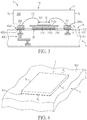
- FIG. 1 is a schematic, cross-sectional diagram showing an exemplary leadframe chip package 1 in accordance with an embodiment of the invention.
- FIG. 2 is a perspective view of the flipped leadframe chip package 1 of FIG. 1 .
- the leadframe chip package 1 such as a QFN package may comprise a plurality of lead terminals (or pins) 200 disposed around a die attach pad 210 that is supported in a central region of the leadframe chip package 1.
- the leadframe chip package 1 may have a rectangular outline.
- the leadframe chip package 1 may have a top surface 1a, a bottom surface 1b, and four sidewalls S 1 -S 4 between the top surface 1a and the bottom surface 1b.
- the first sidewall S 1 is opposite to the third sidewall S 3 and the second sidewall S 2 is opposite to the fourth sidewall S 4 .
- a ground ring 220 may be disposed between the plurality of lead terminals 200 and the die attach pad 210. It is to be understood that the number of lead terminals and dimension of the leadframe chip package are for illustration purposes only.
- At least one semiconductor die 10 is mounted on a top surface 210a of the die attach pad 210.
- the semiconductor die 10 comprises a plurality of input/output (I/O) pads 101 disposed along the perimeter of the semiconductor die 10.
- the I/O pads 101 of the semiconductor die 10 may be electrically connected to the lead terminals 200 by bond wires 131.
- the plurality of lead terminals 200, the semiconductor die 10, the bond wires 131, and the die attach pad 210 are encapsulated by a molding compound 300 comprising, for example, epoxy resin and filler.
- the at least one semiconductor die 10 may be installed within the package in a flip-chip manner.
- a step cut ST is sawn into the molding compound 300 along the perimeter of the bottom surface 1b of the leadframe chip package 1.
- the step cut ST may penetrate through an entire thickness of each of the plurality of lead terminals 200. Therefore, each of the plurality of lead terminals 200 has at least an exposed outer end 200a, or flank, at the step cut ST.
- the exposed outer ends 200a are retracted and shaded at the step cut ST and therefore do not present on the four sidewalls S 1 -S 4 of the leadframe chip package 1.
- the leadframe chip package 1 may have a thickness t that is greater than 0.4mm.
- the leadframe chip package 1 may have a thickness t of about 1.0-2.0 mm, for example, 1.4 mm.
- the step cut ST may have a height h of about 0.1-0.3 mm, for example, 0.2 mm, and a width d of about 0.2-0.4 mm, for example, 0.3 mm, but is not limited thereto.
- the height h of the step cut ST may be greater than a thickness of the plurality of lead terminals 200.
- a bottom surface 210b of the die attach pad 210 may be exposed from the bottom surface 1b of the leadframe chip package 1 and may be connected to a ground plane and/or heat-dissipating plugs (not shown) in a printed circuit board (PCB).
- the ground ring 220 is half-etched from the bottom surface 1b and is not exposed from the bottom surface 1b of the leadframe chip package 1.
- FIG. 3 is a schematic, cross-sectional diagram showing an exemplary printed circuit board assembly (PCBA) in accordance with one embodiment of the invention.
- FIG. 4 is a perspective partial view of the PCBA in FIG. 3 .
- PCBA printed circuit board assembly
- the PCBA 5 comprises the leadframe chip package 1 as set forth in FIG. 1 and FIG. 2 , and a printed circuit board 4.
- the leadframe chip package 1 is soldered to the printed circuit board 4.
- the printed circuit board 4 may be a laminated board made of insulating material layers 410 and layers of metal traces 420 such as copper traces separated by the insulating material layers 410.
- the metal traces 420 may function to establish electrical connections between devices mounted on the printed circuit board 4, conduct heat, or provide a ground.
- bonding pads 420p are provided and solder openings 412a are formed in a solder mask 412 to define soldering regions on the bonding pads 420p, respectively.
- solder paste SP can be applied to the surface of the bonding pads 420p within the defined regions.
- the solder paste SP can be applied onto the printed circuit board 4 by stencil printing methods, but not limited thereto.
- the leadframe chip package 1 can be positioned on the printed circuit board 4, and the PCBA 5 can be placed into an oven and heated. The heating cause the solder to melt, leading to wetting and wicking.
- the solder mask 412 on the printed circuit board 4 can control the solder paste SP during heating.
- the solder mask 412 is placed on the printed circuit board 4, and solder paste SP is applied to areas of the printed circuit board 4 to which the leadframe chip package 1 is to be attached that are not protected by the solder mask 412.
- a solder fillet F may be observed on the exposed outer end 200a at the step cut ST.
- the solder fillet F does not protrude beyond the four sidewalls S 1 -S 4 .
- the solder fillet F is in direct contact with the exposed outer end 200a.
- the solder fillet F wicking up to the exposed outer end 200a may have a half-spherical profile or a curved outer surface, but is not limited thereto.
- the exposed outer end 200a and the solder fillet F are shaded by the molding compound 300 at the step cut ST. It is to be understood that in some embodiments the solder fillet F may not be observed on the exposed outer end 200a depending upon the design of the PCB.
- FIG. 2 is a continuous ring-shaped region recessed into the molding compound 300 along the perimeter of the bottom surface 1b of the leadframe chip package 1, it is understood that in some cases the step cut ST may be a discontinuous region depending upon the design requirements.
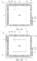
- FIG. 5A to FIG. 5F are bottom views of the leadframe chip packages according to various embodiments of the invention, wherein like layers, regions, or elements are designated by like numeral numbers or labels.
- the step cut ST is a continuous ring-shaped region recessed into the molding compound 300 along the perimeter of the bottom surface 1b of the leadframe chip package 1.
- the cut ends 200a of the lead terminals 200 are not exposed on the sidewalls S 1 -S 4 .
- the step cut ST is a C-shaped region sawn into the molding compound 300 along the perimeter of the bottom surface 1b of the leadframe chip package 1 and is formed only under the three sidewalls S 2 -S 4 .
- the lead terminals 201 have cut ends 201a exposed from the sidewall S 1 .
- the step cut ST is a discontinuous ring-shaped region sawn into the molding compound 300 along the perimeter of the bottom surface 1b of the leadframe chip package 1.
- the lead terminals 201 have cut ends 201a exposed from the sidewall S 1 .
- the lead terminals 201 may have a length that is different from that of the lead terminals 200.
- the leadframe chip package 1 comprises L-shaped step cut ST 1 and step cut ST 2 sawn into the molding compound 300 along the perimeter of the bottom surface 1b of the leadframe chip package 1.
- the lead terminals 201 have cut ends 201a exposed from the sidewalls S 1 and S 3 .
- the lead terminals 201 may have a length that is different from that of the lead terminals 200.
- the leadframe chip package 1 comprises step cut ST only adjacent to the sidewall S 4 .
- the lead terminals 201 have cut ends 201a exposed from the sidewalls S 1 , S 3 and S 2 .
- the leadframe chip package 1 comprises step cut ST 1 adjacent to the sidewall S 4 and step cut ST 2 adjacent to the sidewall S 2 .
- the lead terminals 201 have cut ends 201a exposed from the sidewalls S 1 and S 3 .
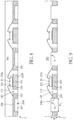
- FIG. 6 to FIG. 10 are schematic, cross-sectional diagrams showing a method for fabricating the leadframe chip package 1 in FIG. 1 and FIG. 2 according to an embodiment of the invention, wherein like layers, regions, or elements are designated by like numeral numbers or labels.
- a leadframe strip (or carrier) 2 populated with a plurality of leadframes 20 is provided.
- the leadframe strip 2 may be composed of a metal sheet or metal layer, for example, a copper layer.
- Each of the plurality of leadframes 20 comprises a die attach pad 210 supported in a central region and lead terminals 200 disposed around the die attach pad 210.
- the die attach pad 210 may be supported by four tie-bars extending at the four corners and a gap GP may be formed between the die attach pad 210 and the lead terminals 200.
- the leadframes 20 may comprise half-etched regions 200r between the lead terminals 200.
- the half-etched regions 200r are disposed under connecting portions 206.
- a semiconductor die 10 is mounted on a top surface 210a of the die attach pad 210.
- the semiconductor die 10 may be secured to the top surface 210a of the die attach pad 210 by using an adhesive layer 110, but is not limited thereto.
- the semiconductor die 10 comprises a plurality of I/O pads 101 disposed along the perimeter of the semiconductor die 10.
- the I/O pads 101 of the semiconductor die 10 may be electrically connected to the lead terminals 200 by bond wires 131.
- the plurality of lead terminals 200, the semiconductor die 10, the bond wires 131, and the die attach pad 210 are encapsulated by a molding compound 300.
- the molding compound 300 may comprise, for example, epoxy resin and filler, but not limited thereto.
- a bottom surface 210b of the die attach pad 210 may be exposed.
- the half-etched regions 200r and the gap GP may be filled with the molding compound 300.
- a step cut ST is sawn into the molding compound 300 along the perimeter around the lead terminals 200.
- the molding compound 300 within the half-etched regions 200r is removed.
- the connecting portions 206 are removed.
- the step cut ST may be formed by using a step cut saw width W 1 .
- the step cut saw width W 1 may be approximately 0.9 mm, but not limited thereto.
- the step cut ST may have a height h of about 0.1-0.3 mm, for example, 0.2 mm.
- the height h of the step cut ST may be greater than a thickness of the plurality of lead terminals 200.
- each of the lead terminals 200 has an exposed outer end 200a, or flank, at the step cut ST.
- a sawing process is performed to saw through the molding compound 300 along the step cut ST.
- the sawing process may be performed using a saw width W 2 less than the step cut saw width W 1 .
- the saw width W 2 is approximately 0.2-0.4 mm, for example, 0.3 mm.
- FIG. 11 to FIG. 15 are schematic, cross-sectional diagrams showing a method for fabricating a leadframe chip package according to another embodiment of the invention, wherein like layers, regions, or elements are designated by like numeral numbers or labels.
- a leadframe strip 2 populated with a plurality of leadframes 20 is provided.
- Each of the plurality of leadframes 20 comprises a die attach pad 210 supported in a central region and lead terminals 200 disposed around the die attach pad 210.
- the die attach pad 210 may be supported by four tie-bars extending at the four corners and a gap GP may be formed between the die attach pad 210 and the lead terminals 200.
- the leadframes 20 may comprise half-etched regions 200r between the lead terminals 200.
- the half-etched regions 200r are disposed under connecting portions 206.
- a semiconductor die 10 is mounted on a top surface 210a of the die attach pad 210.
- the semiconductor die 10 may be secured to the top surface 210a of the die attach pad 210 by using an adhesive layer 110, but is not limited thereto.
- the semiconductor die 10 comprises a plurality of I/O pads 101 disposed along the perimeter of the semiconductor die 10.
- the I/O pads 101 of the semiconductor die 10 may be electrically connected to the lead terminals 200 by bond wires 131.
- the plurality of lead terminals 200, the semiconductor die 10, the bond wires 131, and the die attach pad 210 are encapsulated by a molding compound 300.
- the molding compound 300 may comprise, for example, epoxy resin and filler, but not limited thereto.
- a bottom surface 210b of the die attach pad 210 may be exposed.
- the half-etched regions 200r and the gap GP may be filled with the molding compound 300.
- a step cut ST is sawn into the molding compound 300 along the perimeter around the lead terminals 200.
- the step cut ST may be formed by using a step cut saw width W 3 .
- the step cut saw width W 3 may be smaller than 0.9 mm, but not limited thereto.
- the step cut ST may have a height h of about 0.1-0.3 mm, for example, 0.2 mm.
- the height h of the step cut ST may be greater than a thickness of the plurality of lead terminals 200.
- the molding compound 300 within the half-etched regions 200r is not completely removed. The remaining portion 306 of the molding compound 300 within the half-etched regions 200r masks the side surface of the lead terminals 200.
- the connecting portions 206 are cut through, thereby exposing the end surfaces 206a above the remaining portion 306 of the molding compound 300 within the half-etched regions 200r.
- a sawing process is performed to saw through the molding compound 300 along the step cut ST.
- the sawing process may be performed using a saw width W 2 less than the step cut saw width W 3 .
Landscapes
- Lead Frames For Integrated Circuits (AREA)
- Structures Or Materials For Encapsulating Or Coating Semiconductor Devices Or Solid State Devices (AREA)
Abstract
Description
- This application claims priority from
U.S. provisional application No. 62/930,092 filed on November 4, 2019 - This invention relates generally to a semiconductor package, and in particular to an improved leadframe chip package secure to physical probing or hardware hacking.
- Many integrated circuits are used to store sensitive or confidential information such as personal or financial information. The technology for reverse engineering an integrated circuit (IC) has progressed to the point where the state of individual circuits can be read off of an operating microcircuit. For example, a leadframe chip package such as a quad flat no-lead (QFN) package typically has pins (or perimeter lands) located on the edge of the package and is susceptible to physical probing or hardware hacking.
- Protection of integrated circuits from such intrusions, which may allow access to the sensitive or confidential information, is becoming increasingly important. Therefore, there is a constant need in this industry to provide an improved leadframe chip package capable of reducing the ability of a hacker to physically probe an IC package with such perimeter lands.
- It is one object of the invention to provide an improved leadframe chip package with shaded lead terminals. A semiconductor package according to the invention is defined in
independent claim 1, a printed circuit board assembly according to the invention is defined in claim 6, and a method for fabricating a semiconductor package according to the invention is defined inindependent claim 10. The dependent claims define preferred embodiments thereof. - According to one aspect of the invention, a semiconductor package includes a die attach pad; a plurality of lead terminals disposed around the die attach pad; a semiconductor die mounted on the die attach pad; a molding compound encapsulating the plurality of lead terminals, the semiconductor die, and the die attach pad; and a step cut sawn into the molding compound along a perimeter of a bottom surface of the semiconductor package. The step cut penetrates through an entire thickness of each of the plurality of lead terminals, whereby each of the plurality of lead terminals has at least an exposed outer end at the step cut.
- Preferably, the semiconductor die comprises a plurality of input/output (I/O) pads disposed along a perimeter of the semiconductor die, and wherein the plurality of I/O pads of the semiconductor die is electrically connected to the lead terminals by bond wires.
- Preferably, the semiconductor package has a thickness greater than 0.4 mm.
- Preferably, the step cut has a height greater than the thickness of each of the plurality of lead terminals and a width of about 0.2-0.4 mm.
- Preferably, a bottom surface of the die attach pad is exposed from the bottom surface of the semiconductor package.
- Preferably, a remaining portion of the molding compound masks a side surface of the lead terminals.
- According to another aspect of the invention, a printed circuit board assembly includes a printed circuit board comprising a chip-mounting face; and a semiconductor package mounted on the chip-mounting face. The semiconductor package has a rectangular outline, a top surface, a bottom surface, and four sidewalls between the top surface and the bottom surface.
- The semiconductor package includes a die attach pad; a plurality of lead terminals disposed around the die attach pad; a semiconductor die mounted on the die attach pad; a molding compound encapsulating the plurality of lead terminals, the semiconductor die, and the die attach pad; and a step cut sawn into the molding compound along a perimeter of a bottom surface of the semiconductor package. The step cut penetrates through an entire thickness of each of the plurality of lead terminals, whereby each of the plurality of lead terminals has at least an exposed outer end at the step cut. The semiconductor package may include the preferred features described above.
- Preferably, a solder fillet is provided on the exposed outer end at the step cut.
- Preferably, the solder fillet does not protrude beyond the four sidewalls of the semiconductor package.
- Preferably, the solder fillet is in direct contact with the exposed outer end and has a half-spherical profile or a curved outer surface.
- Preferably, the exposed outer end and the solder fillet are shaded by the molding compound at the step cut.
- Preferably, a remaining portion of the molding compound masks a side surface of the lead terminals.
- According to another aspect of the invention, a method for fabricating a semiconductor package is provided. A leadframe strip populated with a plurality of leadframes is provided. Each of the plurality of leadframes comprises a die attach pad supported in a central region and lead terminals disposed around the die attach pad. A semiconductor die is mounted on the die attach pad. The semiconductor die is electrically coupling with the lead terminals. The lead terminals, the semiconductor die, and the die attach pad are encapsulated with a molding compound. A step cut is sawn into the molding compound along a perimeter around the lead terminals using a step cut saw width. A sawing process is performed to saw through the molding compound along the step cut using saw width, wherein the step cut saw width is wider than the saw width.
- According to some embodiments, the semiconductor die comprises a plurality of input/output (I/O) pads disposed along a perimeter of the semiconductor die, and wherein the plurality of I/O pads of the semiconductor die is electrically connected to the lead terminals by bond wires.
- Preferably, the leadframes comprise half-etched regions between the lead terminals.
- Preferably, the lead terminals are connected by connecting portions, and wherein the half-etched regions are disposed under the connecting portions.
- Preferably, the molding compound within the half-etched regions is removed, and the connecting portions are removed when sawing the step cut into the molding compound.
- Preferably, the step cut saw width is approximately 0.9 mm and the saw width is approximately 0.2-0.4 mm.
- These and other objectives of the present invention will no doubt become obvious to those of ordinary skill in the art after reading the following detailed description of the preferred embodiment that is illustrated in the various figures and drawings.
- The accompanying drawings are included to provide a further understanding of the invention and are incorporated in and constitute a part of this specification. The drawings illustrate embodiments of the invention and, together with the description, serve to explain the principles of the invention. In the drawings:
-
FIG. 1 is a schematic, cross-sectional diagram showing an exemplary leadframe chip package in accordance with an embodiment of the invention; -
FIG. 2 is a perspective view of the flipped leadframe chip package ofFIG. 1 ; -
FIG. 3 is a schematic, cross-sectional diagram showing an exemplary printed circuit board assembly (PCBA) in accordance with one embodiment of the invention; -
FIG. 4 is a perspective partial view of the PCBA inFIG. 3 ; -
FIG. 5A to FIG. 5F are bottom views of the leadframe chip packages according to various embodiments of the invention; -
FIG. 6 to FIG. 10 are schematic, cross-sectional diagrams showing a method for fabricating the leadframe chip package inFIG. 1 and FIG. 2 according to an embodiment of the invention; and -
FIG. 11 to FIG. 15 are schematic, cross-sectional diagrams showing a method for fabricating a leadframe chip package according to another embodiment of the invention. - In the following detailed description of embodiments of the invention, reference is made to the accompanying drawings, which form a part hereof, and in which is shown by way of illustration specific preferred embodiments in which the disclosure may be practiced.
- These embodiments are described in sufficient detail to enable those skilled in the art to practice them, and it is to be understood that other embodiments may be utilized and that mechanical, chemical, electrical, and procedural changes may be made without departing from the spirit and scope of the present disclosure. The following detailed description is, therefore, not to be taken in a limiting sense, and the scope of embodiments of the present invention is defined only by the appended claims.
- It will be understood that when an element or layer is referred to as being "on", "connected to" or "coupled to" another element or layer, it can be directly on, connected or coupled to the other element or layer or intervening elements or layers may be present. In contrast, when an element is referred to as being "directly on," "directly connected to" or "directly coupled to" another element or layer, there are no intervening elements or layers present. Like numbers refer to like elements throughout. As used herein, the term "and/or" includes any and all combinations of one or more of the associated listed items.
- There are various leadframe-based surface mount components, such as quad flat no-lead (QFN) package, advanced QFN (aQFN) package, low-profile quad flat package (LQFP) or the like. A package can be attached to a printed circuit board (PCB) by, for example, soldering it to the PCB. The attachment of the packages (i.e. packaged integrated circuit) to PCBs produces printed circuit board assemblies (PCBAs), which can be used as motherboards in computers, portable devices such as mobile phone, tablets, notebooks, etc.
- Generally, a leadframe strip is populated with a plurality of leadframes. A semiconductor die or microelectronic device may be mounted on each leadframe and encapsulated with a molding compound. Leadframes are separated during singulation of the strip to create individual semiconductor packages. One type of the semiconductor packages is a flat-pack no-lead package where each terminal is exposed at a bottom and at a side of the package. Typically, the sawing process during singulation of the strip typically results in lead terminals that have at least some exposed base metal on a cut end, or flank, of each lead terminal. Typically, the aforesaid cut end is vertically flush with a sidewall surface of the package or the sidewall surface of a molding compound.
- The term of quad flat no-lead or small outline no-lead package indicates that the leads do not have cantilevered leads, but flat leads, which are typically arrayed along the periphery of the packaged device. The metal of the leads may be connected by solder material to the metal of respective contact pads of an external part. QFN packages typically use a copper leadframe for the die assembly and PCB interconnection.
- Please refer to
FIG. 1 and FIG. 2. FIG. 1 is a schematic, cross-sectional diagram showing an exemplaryleadframe chip package 1 in accordance with an embodiment of the invention.FIG. 2 is a perspective view of the flippedleadframe chip package 1 ofFIG. 1 . As shown inFIG. 1 and FIG. 2 , theleadframe chip package 1 such as a QFN package may comprise a plurality of lead terminals (or pins) 200 disposed around a die attachpad 210 that is supported in a central region of theleadframe chip package 1. Theleadframe chip package 1 may have a rectangular outline. Theleadframe chip package 1 may have a top surface 1a, abottom surface 1b, and four sidewalls S1-S4 between the top surface 1a and thebottom surface 1b. The first sidewall S1 is opposite to the third sidewall S3 and the second sidewall S2 is opposite to the fourth sidewall S4. Optionally, aground ring 220 may be disposed between the plurality oflead terminals 200 and the die attachpad 210. It is to be understood that the number of lead terminals and dimension of the leadframe chip package are for illustration purposes only. - Preferably, at least one semiconductor die 10 is mounted on a
top surface 210a of the die attachpad 210. The semiconductor die 10 comprises a plurality of input/output (I/O)pads 101 disposed along the perimeter of the semiconductor die 10. Preferably, for example, the I/O pads 101 of the semiconductor die 10 may be electrically connected to thelead terminals 200 bybond wires 131. The plurality oflead terminals 200, the semiconductor die 10, thebond wires 131, and the die attachpad 210 are encapsulated by amolding compound 300 comprising, for example, epoxy resin and filler. In some embodiments, the at least one semiconductor die 10 may be installed within the package in a flip-chip manner. - Preferably, a step cut ST is sawn into the
molding compound 300 along the perimeter of thebottom surface 1b of theleadframe chip package 1. The step cut ST may penetrate through an entire thickness of each of the plurality oflead terminals 200. Therefore, each of the plurality oflead terminals 200 has at least an exposedouter end 200a, or flank, at the step cut ST. The exposedouter ends 200a are retracted and shaded at the step cut ST and therefore do not present on the four sidewalls S1-S4 of theleadframe chip package 1. - Preferably, the
leadframe chip package 1 may have a thickness t that is greater than 0.4mm. Alternatively preferably, theleadframe chip package 1 may have a thickness t of about 1.0-2.0 mm, for example, 1.4 mm.Preferably, the step cut ST may have a height h of about 0.1-0.3 mm, for example, 0.2 mm, and a width d of about 0.2-0.4 mm, for example, 0.3 mm, but is not limited thereto. Preferably, the height h of the step cut ST may be greater than a thickness of the plurality oflead terminals 200. - Preferably, a
bottom surface 210b of the die attachpad 210 may be exposed from thebottom surface 1b of theleadframe chip package 1 and may be connected to a ground plane and/or heat-dissipating plugs (not shown) in a printed circuit board (PCB). Preferably, theground ring 220 is half-etched from thebottom surface 1b and is not exposed from thebottom surface 1b of theleadframe chip package 1. - Please briefly to
FIG. 3 and FIG. 4. FIG. 3 is a schematic, cross-sectional diagram showing an exemplary printed circuit board assembly (PCBA) in accordance with one embodiment of the invention.FIG. 4 is a perspective partial view of the PCBA inFIG. 3 . - As shown in
FIG. 3 , thePCBA 5 comprises theleadframe chip package 1 as set forth inFIG. 1 and FIG. 2 , and a printed circuit board 4. Theleadframe chip package 1 is soldered to the printed circuit board 4. Preferably, the printed circuit board 4 may be a laminated board made of insulating material layers 410 and layers of metal traces 420 such as copper traces separated by the insulating material layers 410. The metal traces 420 may function to establish electrical connections between devices mounted on the printed circuit board 4, conduct heat, or provide a ground. On a chip-mountingface 4a of the printed circuit board 4,bonding pads 420p are provided andsolder openings 412a are formed in asolder mask 412 to define soldering regions on thebonding pads 420p, respectively. - To solder the
leadframe chip package 1 to the printed circuit board 4, solder paste SP can be applied to the surface of thebonding pads 420p within the defined regions. The solder paste SP can be applied onto the printed circuit board 4 by stencil printing methods, but not limited thereto. After the application of solder paste SP, theleadframe chip package 1 can be positioned on the printed circuit board 4, and thePCBA 5 can be placed into an oven and heated. The heating cause the solder to melt, leading to wetting and wicking. Thesolder mask 412 on the printed circuit board 4 can control the solder paste SP during heating. Thesolder mask 412 is placed on the printed circuit board 4, and solder paste SP is applied to areas of the printed circuit board 4 to which theleadframe chip package 1 is to be attached that are not protected by thesolder mask 412. - Preferably, a solder fillet F may be observed on the exposed
outer end 200a at the step cut ST. Preferably, the solder fillet F does not protrude beyond the four sidewalls S1-S4. Preferably, the solder fillet F is in direct contact with the exposedouter end 200a. Preferably, the solder fillet F wicking up to the exposedouter end 200a may have a half-spherical profile or a curved outer surface, but is not limited thereto. As can be discerned fromFIG. 4 , the exposedouter end 200a and the solder fillet F are shaded by themolding compound 300 at the step cut ST. It is to be understood that in some embodiments the solder fillet F may not be observed on the exposedouter end 200a depending upon the design of the PCB. - Although the step cut ST shown in
FIG. 2 is a continuous ring-shaped region recessed into themolding compound 300 along the perimeter of thebottom surface 1b of theleadframe chip package 1, it is understood that in some cases the step cut ST may be a discontinuous region depending upon the design requirements.FIG. 5A to FIG. 5F are bottom views of the leadframe chip packages according to various embodiments of the invention, wherein like layers, regions, or elements are designated by like numeral numbers or labels. - As shown in
FIG. 5A , the step cut ST is a continuous ring-shaped region recessed into themolding compound 300 along the perimeter of thebottom surface 1b of theleadframe chip package 1. The cut ends 200a of thelead terminals 200 are not exposed on the sidewalls S1-S4. - As shown in
FIG. 5B , the step cut ST is a C-shaped region sawn into themolding compound 300 along the perimeter of thebottom surface 1b of theleadframe chip package 1 and is formed only under the three sidewalls S2-S4. Thelead terminals 201 have cutends 201a exposed from the sidewall S1. - As shown in
FIG. 5C , the step cut ST is a discontinuous ring-shaped region sawn into themolding compound 300 along the perimeter of thebottom surface 1b of theleadframe chip package 1. At the discontinuity, thelead terminals 201 have cutends 201a exposed from the sidewall S1. Thelead terminals 201 may have a length that is different from that of thelead terminals 200. - As shown in
FIG. 5D , theleadframe chip package 1 comprises L-shaped step cut ST1 and step cut ST2 sawn into themolding compound 300 along the perimeter of thebottom surface 1b of theleadframe chip package 1. At the discontinuity, thelead terminals 201 have cutends 201a exposed from the sidewalls S1 and S3. Thelead terminals 201 may have a length that is different from that of thelead terminals 200. - As shown in
FIG. 5E , theleadframe chip package 1 comprises step cut ST only adjacent to the sidewall S4. Thelead terminals 201 have cutends 201a exposed from the sidewalls S1, S3 and S2. - As shown in
FIG. 5F , theleadframe chip package 1 comprises step cut ST1 adjacent to the sidewall S4 and step cut ST2 adjacent to the sidewall S2. Thelead terminals 201 have cutends 201a exposed from the sidewalls S1 and S3. -
FIG. 6 to FIG. 10 are schematic, cross-sectional diagrams showing a method for fabricating theleadframe chip package 1 inFIG. 1 and FIG. 2 according to an embodiment of the invention, wherein like layers, regions, or elements are designated by like numeral numbers or labels. - As shown in
FIG. 6 , a leadframe strip (or carrier) 2 populated with a plurality ofleadframes 20 is provided. Preferably, theleadframe strip 2 may be composed of a metal sheet or metal layer, for example, a copper layer. Each of the plurality ofleadframes 20 comprises a die attachpad 210 supported in a central region andlead terminals 200 disposed around the die attachpad 210. Although not shown in the figures, it is understood that the die attachpad 210 may be supported by four tie-bars extending at the four corners and a gap GP may be formed between the die attachpad 210 and thelead terminals 200. Preferably, theleadframes 20 may comprise half-etchedregions 200r between thelead terminals 200. Preferably, the half-etchedregions 200r are disposed under connectingportions 206. - As shown in
FIG. 7 , asemiconductor die 10 is mounted on atop surface 210a of the die attachpad 210. For example, the semiconductor die 10 may be secured to thetop surface 210a of the die attachpad 210 by using anadhesive layer 110, but is not limited thereto. The semiconductor die 10 comprises a plurality of I/O pads 101 disposed along the perimeter of the semiconductor die 10. Preferably, for example, the I/O pads 101 of the semiconductor die 10 may be electrically connected to thelead terminals 200 bybond wires 131. - As shown in
FIG. 8 , the plurality oflead terminals 200, the semiconductor die 10, thebond wires 131, and the die attachpad 210 are encapsulated by amolding compound 300. Preferably, themolding compound 300 may comprise, for example, epoxy resin and filler, but not limited thereto. Preferably, abottom surface 210b of the die attachpad 210 may be exposed. Preferably, the half-etchedregions 200r and the gap GP may be filled with themolding compound 300. - As shown in
FIG. 9 , a step cut ST is sawn into themolding compound 300 along the perimeter around thelead terminals 200. Preferably, themolding compound 300 within the half-etchedregions 200r is removed. Preferably, the connectingportions 206 are removed. The step cut ST may be formed by using a step cut saw width W1. Preferably, the step cut saw width W1 may be approximately 0.9 mm, but not limited thereto. Preferably, the step cut ST may have a height h of about 0.1-0.3 mm, for example, 0.2 mm. Preferably, the height h of the step cut ST may be greater than a thickness of the plurality oflead terminals 200. Preferably, after the step cut ST is formed, each of thelead terminals 200 has an exposedouter end 200a, or flank, at the step cut ST. - As shown in
FIG. 10 , subsequently, a sawing process is performed to saw through themolding compound 300 along the step cut ST. Preferably, the sawing process may be performed using a saw width W2 less than the step cut saw width W1. Preferably, the saw width W2 is approximately 0.2-0.4 mm, for example, 0.3 mm. -
FIG. 11 to FIG. 15 are schematic, cross-sectional diagrams showing a method for fabricating a leadframe chip package according to another embodiment of the invention, wherein like layers, regions, or elements are designated by like numeral numbers or labels. - As shown in
FIG. 11 , aleadframe strip 2 populated with a plurality ofleadframes 20 is provided. Each of the plurality ofleadframes 20 comprises a die attachpad 210 supported in a central region andlead terminals 200 disposed around the die attachpad 210. Although not shown in the figures, it is understood that the die attachpad 210 may be supported by four tie-bars extending at the four corners and a gap GP may be formed between the die attachpad 210 and thelead terminals 200. Preferably, theleadframes 20 may comprise half-etchedregions 200r between thelead terminals 200. Preferably, the half-etchedregions 200r are disposed under connectingportions 206. - As shown in
FIG. 12 , asemiconductor die 10 is mounted on atop surface 210a of the die attachpad 210. For example, the semiconductor die 10 may be secured to thetop surface 210a of the die attachpad 210 by using anadhesive layer 110, but is not limited thereto. The semiconductor die 10 comprises a plurality of I/O pads 101 disposed along the perimeter of the semiconductor die 10. Preferably, for example, the I/O pads 101 of the semiconductor die 10 may be electrically connected to thelead terminals 200 bybond wires 131. - As shown in
FIG. 13 , the plurality oflead terminals 200, the semiconductor die 10, thebond wires 131, and the die attachpad 210 are encapsulated by amolding compound 300. Preferably, themolding compound 300 may comprise, for example, epoxy resin and filler, but not limited thereto. Preferably, abottom surface 210b of the die attachpad 210 may be exposed. Preferably, the half-etchedregions 200r and the gap GP may be filled with themolding compound 300. - As shown in
FIG. 14 , a step cut ST is sawn into themolding compound 300 along the perimeter around thelead terminals 200. The step cut ST may be formed by using a step cut saw width W3. Preferably, the step cut saw width W3 may be smaller than 0.9 mm, but not limited thereto. Preferably, the step cut ST may have a height h of about 0.1-0.3 mm, for example, 0.2 mm. Preferably, the height h of the step cut ST may be greater than a thickness of the plurality oflead terminals 200. Preferably, themolding compound 300 within the half-etchedregions 200r is not completely removed. The remainingportion 306 of themolding compound 300 within the half-etchedregions 200r masks the side surface of thelead terminals 200. Preferably, the connectingportions 206 are cut through, thereby exposing theend surfaces 206a above the remainingportion 306 of themolding compound 300 within the half-etchedregions 200r. - As shown in
FIG. 15 , subsequently, a sawing process is performed to saw through themolding compound 300 along the step cut ST. Preferably, the sawing process may be performed using a saw width W2 less than the step cut saw width W3. - Those skilled in the art will readily observe that numerous modifications and alterations of the device and method may be made while retaining the teachings of the invention. Accordingly, the above disclosure should be construed as limited only by the metes and bounds of the appended claims.
Claims (15)
- A semiconductor package (1), comprising:a die attach pad (210);a plurality of lead terminals (200) disposed around the die attach pad (210);a semiconductor die (10) mounted on the die attach pad (210);a molding compound (300) encapsulating the plurality of lead terminals (200), the semiconductor die (10), and the die attach pad (210); anda step cut (ST) sawn into the molding compound (300) along a perimeter of a bottom surface (1b) of the semiconductor package (1), wherein the step cut penetrates through an entire thickness of each of the plurality of lead terminals (200), whereby each of the plurality of lead terminals (200) has at least an exposed outer end (200a) at the step cut (ST).
- The semiconductor package according to claim 1, wherein the semiconductor die (10) comprises a plurality of input/output, in the following also referred to as I/O, pads (101) disposed along a perimeter of the semiconductor die (10), and wherein the plurality of I/O pads (101) of the semiconductor die (10) is electrically connected to the lead terminals (200) by bond wires (131).
- The semiconductor package according to claim 1 or 2, wherein the semiconductor package (1) has a thickness greater than 0.4 mm; and/or
wherein the step cut (ST) has a height (h) greater than the thickness of each of the plurality of lead terminals (200), and a width (d) of about 0.2-0.4 mm. - The semiconductor package according to any one of claims 1 to 3, wherein a bottom surface (210b) of the die attach pad (210) is exposed from the bottom surface (1b) of the semiconductor package (10).
- The semiconductor package according to any one of claims 1 to 4, wherein a remaining portion of the molding compound (300) masks a side surface of the lead terminals (200).
- A printed circuit board assembly (5), comprising:
a printed circuit board (4) comprising a chip-mounting face (4a); and
a semiconductor package (1) according to any one of claims 1 to 5 mounted on the chip-mounting face (4a), wherein the semiconductor package (1) has a rectangular outline, a top surface (1a), the bottom surface (1b), and four sidewalls (S1-S4) between the top surface (1a) and the bottom surface (1b). - The printed circuit board assembly according to claim 6, wherein a solder fillet (F) is provided on the exposed outer end (200a) at the step cut (ST); and/orwherein the solder fillet (F) does not protrude beyond the four sidewalls (S1-S4) of the semiconductor package (1); and/orwherein the solder fillet (F) is in direct contact with the exposed outer end (200a) and has a half-spherical profile or a curved outer surface.
- The printed circuit board assembly according to claim 7, wherein the exposed outer end (200a) and the solder fillet (F) are shaded by the molding compound (300) at the step cut (ST).
- The printed circuit board assembly according to claim 7 or 8, wherein a remaining portion of the molding compound (300) masks a side surface of the lead terminals (200).
- A method for fabricating a semiconductor package (1), comprising:providing a leadframe strip (2) populated with a plurality of leadframes (20), wherein each of the plurality of leadframes (20) comprises a die attach pad (210) supported in a central region and lead terminals (200) disposed around the die attach pad (210);mounting a semiconductor die (10) on the die attach pad (210);electrically coupling the semiconductor die (10) with the lead terminals (200);encapsulating the lead terminals (200), the semiconductor die (10), and the die attach pad (210) with a molding compound (300);sawing a step cut (ST) into the molding compound (300) along a perimeter around the lead terminals (200) using a step cut saw width; andperforming a sawing process to saw through the molding compound (300) along the step cut (ST) using a saw width, wherein the step cut saw width is wider than the saw width.
- The method according to claim 10, wherein the semiconductor die (10) comprises a plurality of input/output, in the following also referred to as I/O, pads (101) disposed along a perimeter of the semiconductor die (10), and wherein the plurality of I/O pads (101) of the semiconductor die (10) is electrically connected to the lead terminals (200) by bond wires (131).
- The method according to claim 10 or 11, wherein the leadframes (20) comprise half-etched regions (200r) between the lead terminals (200).
- The method according to claim 12, wherein the lead terminals (200) are connected by connecting portions (206), and wherein the half-etched regions (200r) are disposed under the connecting portions (206).
- The method according to claim 13, wherein the molding compound (300) within the half-etched regions (200r) is removed, and the connecting portions (206) are removed when sawing the step cut (ST) into the molding compound (300).
- The method according to any one of claims 10 to 14, wherein the step cut saw width is approximately 0.9 mm and the saw width is approximately 0.2-0.4 mm.
Applications Claiming Priority (2)
| Application Number | Priority Date | Filing Date | Title |
|---|---|---|---|
| US201962930092P | 2019-11-04 | 2019-11-04 | |
| US17/070,885 US11562948B2 (en) | 2019-11-04 | 2020-10-14 | Semiconductor package having step cut sawn into molding compound along perimeter of the semiconductor package |
Publications (3)
| Publication Number | Publication Date |
|---|---|
| EP3817033A2 true EP3817033A2 (en) | 2021-05-05 |
| EP3817033A3 EP3817033A3 (en) | 2021-05-12 |
| EP3817033B1 EP3817033B1 (en) | 2024-09-18 |
Family
ID=73039815
Family Applications (1)
| Application Number | Title | Priority Date | Filing Date |
|---|---|---|---|
| EP20204309.7A Active EP3817033B1 (en) | 2019-11-04 | 2020-10-28 | Semiconductor package and fabrication method thereof |
Country Status (4)
| Country | Link |
|---|---|
| US (2) | US11562948B2 (en) |
| EP (1) | EP3817033B1 (en) |
| CN (1) | CN112786580A (en) |
| TW (1) | TWI794670B (en) |
Families Citing this family (5)
| Publication number | Priority date | Publication date | Assignee | Title |
|---|---|---|---|---|
| US12354918B2 (en) * | 2021-09-30 | 2025-07-08 | Texas Instruments Incorporated | Package geometries to enable visual inspection of solder fillets |
| US20230411265A1 (en) * | 2022-06-21 | 2023-12-21 | Texas Instruments Incorporated | Split semiconductor package |
| CN117936533A (en) * | 2022-07-19 | 2024-04-26 | 王永明 | Chip and screen integrated device |
| CN117238781B (en) * | 2023-11-16 | 2024-02-23 | 江苏芯德半导体科技有限公司 | Wafer-level ultrathin four-side pin-free chip packaging method and chip packaging structure |
| TWI890408B (en) * | 2024-04-12 | 2025-07-11 | 強茂股份有限公司 | Side wettable package with probe mark and method for making the same |
Family Cites Families (13)
| Publication number | Priority date | Publication date | Assignee | Title |
|---|---|---|---|---|
| US6872599B1 (en) | 2002-12-10 | 2005-03-29 | National Semiconductor Corporation | Enhanced solder joint strength and ease of inspection of leadless leadframe package (LLP) |
| JP4159348B2 (en) | 2002-12-20 | 2008-10-01 | 三洋電機株式会社 | Circuit device manufacturing method |
| JP2006165411A (en) | 2004-12-10 | 2006-06-22 | New Japan Radio Co Ltd | Semiconductor device and manufacturing method thereof |
| US7943431B2 (en) * | 2005-12-02 | 2011-05-17 | Unisem (Mauritius) Holdings Limited | Leadless semiconductor package and method of manufacture |
| US7898067B2 (en) * | 2008-10-31 | 2011-03-01 | Fairchild Semiconductor Corporaton | Pre-molded, clip-bonded multi-die semiconductor package |
| US8841758B2 (en) * | 2012-06-29 | 2014-09-23 | Freescale Semiconductor, Inc. | Semiconductor device package and method of manufacture |
| US9257306B2 (en) | 2013-04-18 | 2016-02-09 | Dai Nippon Printing Co., Ltd. | Lead frame, method for manufacturing lead frame, semiconductor device, and method for manufacturing semiconductor device |
| TWI587548B (en) | 2015-09-07 | 2017-06-11 | 隆達電子股份有限公司 | LED package |
| JP6685112B2 (en) | 2015-11-18 | 2020-04-22 | 株式会社三井ハイテック | Lead frame, lead frame package, and manufacturing method thereof |
| US10366948B2 (en) | 2016-03-17 | 2019-07-30 | Rohm Co., Ltd. | Semiconductor device and method for manufacturing the same |
| JP6761738B2 (en) | 2016-11-15 | 2020-09-30 | 新光電気工業株式会社 | Lead frame and its manufacturing method, manufacturing method of electronic component equipment |
| US10658277B2 (en) | 2017-08-08 | 2020-05-19 | UTAC Headquarters Pte. Ltd. | Semiconductor package with a heat spreader and method of manufacturing thereof |
| CN107946259A (en) | 2017-12-21 | 2018-04-20 | 苏州迈瑞微电子有限公司 | A kind of QFN encapsulating structures and its manufacture method |
-
2020
- 2020-10-14 US US17/070,885 patent/US11562948B2/en active Active
- 2020-10-28 EP EP20204309.7A patent/EP3817033B1/en active Active
- 2020-10-29 CN CN202011182569.6A patent/CN112786580A/en active Pending
- 2020-10-30 TW TW109137748A patent/TWI794670B/en active
-
2022
- 2022-12-20 US US18/084,577 patent/US12205869B2/en active Active
Also Published As
| Publication number | Publication date |
|---|---|
| US20230123668A1 (en) | 2023-04-20 |
| EP3817033B1 (en) | 2024-09-18 |
| CN112786580A (en) | 2021-05-11 |
| US11562948B2 (en) | 2023-01-24 |
| TWI794670B (en) | 2023-03-01 |
| US12205869B2 (en) | 2025-01-21 |
| TW202119577A (en) | 2021-05-16 |
| EP3817033A3 (en) | 2021-05-12 |
| US20210134707A1 (en) | 2021-05-06 |
Similar Documents
| Publication | Publication Date | Title |
|---|---|---|
| US12205869B2 (en) | Method for forming a semiconductor package | |
| JP3032964B2 (en) | Ball grid array semiconductor package and manufacturing method | |
| KR100237328B1 (en) | Structure of semiconductor package and manufacturing method | |
| US6683795B1 (en) | Shield cap and semiconductor package including shield cap | |
| US10943885B2 (en) | Method for making semiconductor device with sidewall recess and related devices | |
| US11869831B2 (en) | Semiconductor package with improved board level reliability | |
| KR100473261B1 (en) | Semiconductor device | |
| US20070085199A1 (en) | Integrated circuit package system using etched leadframe | |
| KR101440933B1 (en) | Integrated circuit package system employing bump technology | |
| US20110068445A1 (en) | Chip package and process thereof | |
| EP0623954B1 (en) | Molded plastic packaging of electronic devices | |
| KR20070034438A (en) | Method of making a stacked die package | |
| CN107946259A (en) | A kind of QFN encapsulating structures and its manufacture method | |
| US20070166884A1 (en) | Circuit board and package structure thereof | |
| US20150041182A1 (en) | Package substrate and chip package using the same | |
| US11233003B2 (en) | Surface mount semiconductor device with a plurality of lead frames | |
| CN116646261A (en) | System-in-package method and package structure with double-sided plastic packaging | |
| JPH10154768A (en) | Semiconductor device and manufacturing method thereof | |
| US8399967B2 (en) | Package structure | |
| JPH07249707A (en) | Semiconductor package | |
| JPH10242362A (en) | Lead frame, semiconductor device, and method of manufacturing semiconductor device | |
| JP2952286B2 (en) | Bare chipless dress package | |
| KR970001889B1 (en) | Lead frame and manufacturing method of semiconductor device having the lead frame | |
| KR100600366B1 (en) | Semiconductor package and manufacturing method thereof | |
| JPH06163760A (en) | Electronic-component mounting board provided with heat-dissipating slug |
Legal Events
| Date | Code | Title | Description |
|---|---|---|---|
| PUAI | Public reference made under article 153(3) epc to a published international application that has entered the european phase |
Free format text: ORIGINAL CODE: 0009012 |
|
| STAA | Information on the status of an ep patent application or granted ep patent |
Free format text: STATUS: THE APPLICATION HAS BEEN PUBLISHED |
|
| PUAL | Search report despatched |
Free format text: ORIGINAL CODE: 0009013 |
|
| AK | Designated contracting states |
Kind code of ref document: A2 Designated state(s): AL AT BE BG CH CY CZ DE DK EE ES FI FR GB GR HR HU IE IS IT LI LT LU LV MC MK MT NL NO PL PT RO RS SE SI SK SM TR |
|
| AK | Designated contracting states |
Kind code of ref document: A3 Designated state(s): AL AT BE BG CH CY CZ DE DK EE ES FI FR GB GR HR HU IE IS IT LI LT LU LV MC MK MT NL NO PL PT RO RS SE SI SK SM TR |
|
| RIC1 | Information provided on ipc code assigned before grant |
Ipc: H01L 21/56 20060101ALI20210407BHEP Ipc: H01L 21/48 20060101AFI20210407BHEP Ipc: H01L 23/31 20060101ALI20210407BHEP Ipc: H01L 23/495 20060101ALI20210407BHEP |
|
| STAA | Information on the status of an ep patent application or granted ep patent |
Free format text: STATUS: REQUEST FOR EXAMINATION WAS MADE |
|
| 17P | Request for examination filed |
Effective date: 20211110 |
|
| RBV | Designated contracting states (corrected) |
Designated state(s): AL AT BE BG CH CY CZ DE DK EE ES FI FR GB GR HR HU IE IS IT LI LT LU LV MC MK MT NL NO PL PT RO RS SE SI SK SM TR |
|
| STAA | Information on the status of an ep patent application or granted ep patent |
Free format text: STATUS: EXAMINATION IS IN PROGRESS |
|
| 17Q | First examination report despatched |
Effective date: 20220803 |
|
| P01 | Opt-out of the competence of the unified patent court (upc) registered |
Effective date: 20230607 |
|
| GRAP | Despatch of communication of intention to grant a patent |
Free format text: ORIGINAL CODE: EPIDOSNIGR1 |
|
| STAA | Information on the status of an ep patent application or granted ep patent |
Free format text: STATUS: GRANT OF PATENT IS INTENDED |
|
| INTG | Intention to grant announced |
Effective date: 20240417 |
|
| GRAS | Grant fee paid |
Free format text: ORIGINAL CODE: EPIDOSNIGR3 |
|
| GRAA | (expected) grant |
Free format text: ORIGINAL CODE: 0009210 |
|
| STAA | Information on the status of an ep patent application or granted ep patent |
Free format text: STATUS: THE PATENT HAS BEEN GRANTED |
|
| AK | Designated contracting states |
Kind code of ref document: B1 Designated state(s): AL AT BE BG CH CY CZ DE DK EE ES FI FR GB GR HR HU IE IS IT LI LT LU LV MC MK MT NL NO PL PT RO RS SE SI SK SM TR |
|
| REG | Reference to a national code |
Ref country code: GB Ref legal event code: FG4D |
|
| REG | Reference to a national code |
Ref country code: CH Ref legal event code: EP |
|
| REG | Reference to a national code |
Ref country code: IE Ref legal event code: FG4D |
|
| REG | Reference to a national code |
Ref country code: DE Ref legal event code: R096 Ref document number: 602020037839 Country of ref document: DE |
|
| REG | Reference to a national code |
Ref country code: LT Ref legal event code: MG9D |
|
| PG25 | Lapsed in a contracting state [announced via postgrant information from national office to epo] |
Ref country code: NO Free format text: LAPSE BECAUSE OF FAILURE TO SUBMIT A TRANSLATION OF THE DESCRIPTION OR TO PAY THE FEE WITHIN THE PRESCRIBED TIME-LIMIT Effective date: 20241218 |
|
| PG25 | Lapsed in a contracting state [announced via postgrant information from national office to epo] |
Ref country code: GR Free format text: LAPSE BECAUSE OF FAILURE TO SUBMIT A TRANSLATION OF THE DESCRIPTION OR TO PAY THE FEE WITHIN THE PRESCRIBED TIME-LIMIT Effective date: 20241219 Ref country code: FI Free format text: LAPSE BECAUSE OF FAILURE TO SUBMIT A TRANSLATION OF THE DESCRIPTION OR TO PAY THE FEE WITHIN THE PRESCRIBED TIME-LIMIT Effective date: 20240918 |
|
| PG25 | Lapsed in a contracting state [announced via postgrant information from national office to epo] |
Ref country code: BG Free format text: LAPSE BECAUSE OF FAILURE TO SUBMIT A TRANSLATION OF THE DESCRIPTION OR TO PAY THE FEE WITHIN THE PRESCRIBED TIME-LIMIT Effective date: 20240918 |
|
| PG25 | Lapsed in a contracting state [announced via postgrant information from national office to epo] |
Ref country code: LV Free format text: LAPSE BECAUSE OF FAILURE TO SUBMIT A TRANSLATION OF THE DESCRIPTION OR TO PAY THE FEE WITHIN THE PRESCRIBED TIME-LIMIT Effective date: 20240918 |
|
| PG25 | Lapsed in a contracting state [announced via postgrant information from national office to epo] |
Ref country code: HR Free format text: LAPSE BECAUSE OF FAILURE TO SUBMIT A TRANSLATION OF THE DESCRIPTION OR TO PAY THE FEE WITHIN THE PRESCRIBED TIME-LIMIT Effective date: 20240918 |
|
| REG | Reference to a national code |
Ref country code: NL Ref legal event code: MP Effective date: 20240918 |
|
| PG25 | Lapsed in a contracting state [announced via postgrant information from national office to epo] |
Ref country code: RS Free format text: LAPSE BECAUSE OF FAILURE TO SUBMIT A TRANSLATION OF THE DESCRIPTION OR TO PAY THE FEE WITHIN THE PRESCRIBED TIME-LIMIT Effective date: 20241218 |
|
| PG25 | Lapsed in a contracting state [announced via postgrant information from national office to epo] |
Ref country code: RS Free format text: LAPSE BECAUSE OF FAILURE TO SUBMIT A TRANSLATION OF THE DESCRIPTION OR TO PAY THE FEE WITHIN THE PRESCRIBED TIME-LIMIT Effective date: 20241218 Ref country code: NO Free format text: LAPSE BECAUSE OF FAILURE TO SUBMIT A TRANSLATION OF THE DESCRIPTION OR TO PAY THE FEE WITHIN THE PRESCRIBED TIME-LIMIT Effective date: 20241218 Ref country code: LV Free format text: LAPSE BECAUSE OF FAILURE TO SUBMIT A TRANSLATION OF THE DESCRIPTION OR TO PAY THE FEE WITHIN THE PRESCRIBED TIME-LIMIT Effective date: 20240918 Ref country code: HR Free format text: LAPSE BECAUSE OF FAILURE TO SUBMIT A TRANSLATION OF THE DESCRIPTION OR TO PAY THE FEE WITHIN THE PRESCRIBED TIME-LIMIT Effective date: 20240918 Ref country code: GR Free format text: LAPSE BECAUSE OF FAILURE TO SUBMIT A TRANSLATION OF THE DESCRIPTION OR TO PAY THE FEE WITHIN THE PRESCRIBED TIME-LIMIT Effective date: 20241219 Ref country code: FI Free format text: LAPSE BECAUSE OF FAILURE TO SUBMIT A TRANSLATION OF THE DESCRIPTION OR TO PAY THE FEE WITHIN THE PRESCRIBED TIME-LIMIT Effective date: 20240918 Ref country code: BG Free format text: LAPSE BECAUSE OF FAILURE TO SUBMIT A TRANSLATION OF THE DESCRIPTION OR TO PAY THE FEE WITHIN THE PRESCRIBED TIME-LIMIT Effective date: 20240918 |
|
| REG | Reference to a national code |
Ref country code: AT Ref legal event code: MK05 Ref document number: 1725433 Country of ref document: AT Kind code of ref document: T Effective date: 20240918 |
|
| PG25 | Lapsed in a contracting state [announced via postgrant information from national office to epo] |
Ref country code: NL Free format text: LAPSE BECAUSE OF FAILURE TO SUBMIT A TRANSLATION OF THE DESCRIPTION OR TO PAY THE FEE WITHIN THE PRESCRIBED TIME-LIMIT Effective date: 20240918 |
|
| PG25 | Lapsed in a contracting state [announced via postgrant information from national office to epo] |
Ref country code: IS Free format text: LAPSE BECAUSE OF FAILURE TO SUBMIT A TRANSLATION OF THE DESCRIPTION OR TO PAY THE FEE WITHIN THE PRESCRIBED TIME-LIMIT Effective date: 20250118 Ref country code: PT Free format text: LAPSE BECAUSE OF FAILURE TO SUBMIT A TRANSLATION OF THE DESCRIPTION OR TO PAY THE FEE WITHIN THE PRESCRIBED TIME-LIMIT Effective date: 20250120 |
|
| PG25 | Lapsed in a contracting state [announced via postgrant information from national office to epo] |
Ref country code: RO Free format text: LAPSE BECAUSE OF FAILURE TO SUBMIT A TRANSLATION OF THE DESCRIPTION OR TO PAY THE FEE WITHIN THE PRESCRIBED TIME-LIMIT Effective date: 20240918 Ref country code: SM Free format text: LAPSE BECAUSE OF FAILURE TO SUBMIT A TRANSLATION OF THE DESCRIPTION OR TO PAY THE FEE WITHIN THE PRESCRIBED TIME-LIMIT Effective date: 20240918 |
|
| PG25 | Lapsed in a contracting state [announced via postgrant information from national office to epo] |
Ref country code: ES Free format text: LAPSE BECAUSE OF FAILURE TO SUBMIT A TRANSLATION OF THE DESCRIPTION OR TO PAY THE FEE WITHIN THE PRESCRIBED TIME-LIMIT Effective date: 20240918 |
|
| PG25 | Lapsed in a contracting state [announced via postgrant information from national office to epo] |
Ref country code: EE Free format text: LAPSE BECAUSE OF FAILURE TO SUBMIT A TRANSLATION OF THE DESCRIPTION OR TO PAY THE FEE WITHIN THE PRESCRIBED TIME-LIMIT Effective date: 20240918 Ref country code: AT Free format text: LAPSE BECAUSE OF FAILURE TO SUBMIT A TRANSLATION OF THE DESCRIPTION OR TO PAY THE FEE WITHIN THE PRESCRIBED TIME-LIMIT Effective date: 20240918 |
|
| PG25 | Lapsed in a contracting state [announced via postgrant information from national office to epo] |
Ref country code: CZ Free format text: LAPSE BECAUSE OF FAILURE TO SUBMIT A TRANSLATION OF THE DESCRIPTION OR TO PAY THE FEE WITHIN THE PRESCRIBED TIME-LIMIT Effective date: 20240918 Ref country code: PL Free format text: LAPSE BECAUSE OF FAILURE TO SUBMIT A TRANSLATION OF THE DESCRIPTION OR TO PAY THE FEE WITHIN THE PRESCRIBED TIME-LIMIT Effective date: 20240918 |
|
| PG25 | Lapsed in a contracting state [announced via postgrant information from national office to epo] |
Ref country code: SK Free format text: LAPSE BECAUSE OF FAILURE TO SUBMIT A TRANSLATION OF THE DESCRIPTION OR TO PAY THE FEE WITHIN THE PRESCRIBED TIME-LIMIT Effective date: 20240918 Ref country code: IT Free format text: LAPSE BECAUSE OF FAILURE TO SUBMIT A TRANSLATION OF THE DESCRIPTION OR TO PAY THE FEE WITHIN THE PRESCRIBED TIME-LIMIT Effective date: 20240918 |
|
| REG | Reference to a national code |
Ref country code: CH Ref legal event code: PL |
|
| REG | Reference to a national code |
Ref country code: DE Ref legal event code: R097 Ref document number: 602020037839 Country of ref document: DE |
|
| PG25 | Lapsed in a contracting state [announced via postgrant information from national office to epo] |
Ref country code: MC Free format text: LAPSE BECAUSE OF FAILURE TO SUBMIT A TRANSLATION OF THE DESCRIPTION OR TO PAY THE FEE WITHIN THE PRESCRIBED TIME-LIMIT Effective date: 20240918 |
|
| PG25 | Lapsed in a contracting state [announced via postgrant information from national office to epo] |
Ref country code: DK Free format text: LAPSE BECAUSE OF FAILURE TO SUBMIT A TRANSLATION OF THE DESCRIPTION OR TO PAY THE FEE WITHIN THE PRESCRIBED TIME-LIMIT Effective date: 20240918 |
|
| PG25 | Lapsed in a contracting state [announced via postgrant information from national office to epo] |
Ref country code: LU Free format text: LAPSE BECAUSE OF NON-PAYMENT OF DUE FEES Effective date: 20241028 Ref country code: BE Free format text: LAPSE BECAUSE OF NON-PAYMENT OF DUE FEES Effective date: 20241031 |
|
| PG25 | Lapsed in a contracting state [announced via postgrant information from national office to epo] |
Ref country code: CH Free format text: LAPSE BECAUSE OF NON-PAYMENT OF DUE FEES Effective date: 20241031 |
|
| PLBE | No opposition filed within time limit |
Free format text: ORIGINAL CODE: 0009261 |
|
| STAA | Information on the status of an ep patent application or granted ep patent |
Free format text: STATUS: NO OPPOSITION FILED WITHIN TIME LIMIT |
|
| REG | Reference to a national code |
Ref country code: BE Ref legal event code: MM Effective date: 20241031 |
|
| 26N | No opposition filed |
Effective date: 20250619 |
|
| PG25 | Lapsed in a contracting state [announced via postgrant information from national office to epo] |
Ref country code: SE Free format text: LAPSE BECAUSE OF FAILURE TO SUBMIT A TRANSLATION OF THE DESCRIPTION OR TO PAY THE FEE WITHIN THE PRESCRIBED TIME-LIMIT Effective date: 20240918 |
|
| PGFP | Annual fee paid to national office [announced via postgrant information from national office to epo] |
Ref country code: GB Payment date: 20250904 Year of fee payment: 6 |
|
| PGFP | Annual fee paid to national office [announced via postgrant information from national office to epo] |
Ref country code: FR Payment date: 20250908 Year of fee payment: 6 |
|
| PG25 | Lapsed in a contracting state [announced via postgrant information from national office to epo] |
Ref country code: IE Free format text: LAPSE BECAUSE OF NON-PAYMENT OF DUE FEES Effective date: 20241028 |
|
| REG | Reference to a national code |
Ref country code: DE Ref legal event code: R079 Ref document number: 602020037839 Country of ref document: DE Free format text: PREVIOUS MAIN CLASS: H01L0021480000 Ipc: H10W0076010000 |
|
| PGFP | Annual fee paid to national office [announced via postgrant information from national office to epo] |
Ref country code: DE Payment date: 20250902 Year of fee payment: 6 |
|
| PG25 | Lapsed in a contracting state [announced via postgrant information from national office to epo] |
Ref country code: HU Free format text: LAPSE BECAUSE OF FAILURE TO SUBMIT A TRANSLATION OF THE DESCRIPTION OR TO PAY THE FEE WITHIN THE PRESCRIBED TIME-LIMIT; INVALID AB INITIO Effective date: 20201028 |
|
| PG25 | Lapsed in a contracting state [announced via postgrant information from national office to epo] |
Ref country code: CY Free format text: LAPSE BECAUSE OF FAILURE TO SUBMIT A TRANSLATION OF THE DESCRIPTION OR TO PAY THE FEE WITHIN THE PRESCRIBED TIME-LIMIT; INVALID AB INITIO Effective date: 20201028 |