EP3816807A1 - Serial communication apparatus and serial communication method - Google Patents
Serial communication apparatus and serial communication method Download PDFInfo
- Publication number
- EP3816807A1 EP3816807A1 EP19826970.6A EP19826970A EP3816807A1 EP 3816807 A1 EP3816807 A1 EP 3816807A1 EP 19826970 A EP19826970 A EP 19826970A EP 3816807 A1 EP3816807 A1 EP 3816807A1
- Authority
- EP
- European Patent Office
- Prior art keywords
- radio frequency
- circuit
- data
- sipi
- valid
- Prior art date
- Legal status (The legal status is an assumption and is not a legal conclusion. Google has not performed a legal analysis and makes no representation as to the accuracy of the status listed.)
- Pending
Links
Images


Classifications
-
- G—PHYSICS
- G06—COMPUTING; CALCULATING OR COUNTING
- G06F—ELECTRIC DIGITAL DATA PROCESSING
- G06F13/00—Interconnection of, or transfer of information or other signals between, memories, input/output devices or central processing units
- G06F13/38—Information transfer, e.g. on bus
- G06F13/382—Information transfer, e.g. on bus using universal interface adapter
- G06F13/385—Information transfer, e.g. on bus using universal interface adapter for adaptation of a particular data processing system to different peripheral devices
-
- G—PHYSICS
- G06—COMPUTING; CALCULATING OR COUNTING
- G06F—ELECTRIC DIGITAL DATA PROCESSING
- G06F13/00—Interconnection of, or transfer of information or other signals between, memories, input/output devices or central processing units
- G06F13/38—Information transfer, e.g. on bus
- G06F13/42—Bus transfer protocol, e.g. handshake; Synchronisation
- G06F13/4282—Bus transfer protocol, e.g. handshake; Synchronisation on a serial bus, e.g. I2C bus, SPI bus
- G06F13/4291—Bus transfer protocol, e.g. handshake; Synchronisation on a serial bus, e.g. I2C bus, SPI bus using a clocked protocol
-
- G—PHYSICS
- G06—COMPUTING; CALCULATING OR COUNTING
- G06F—ELECTRIC DIGITAL DATA PROCESSING
- G06F1/00—Details not covered by groups G06F3/00 - G06F13/00 and G06F21/00
- G06F1/04—Generating or distributing clock signals or signals derived directly therefrom
- G06F1/06—Clock generators producing several clock signals
-
- H—ELECTRICITY
- H04—ELECTRIC COMMUNICATION TECHNIQUE
- H04B—TRANSMISSION
- H04B1/00—Details of transmission systems, not covered by a single one of groups H04B3/00 - H04B13/00; Details of transmission systems not characterised by the medium used for transmission
- H04B1/38—Transceivers, i.e. devices in which transmitter and receiver form a structural unit and in which at least one part is used for functions of transmitting and receiving
- H04B1/40—Circuits
Definitions
- the present invention relates to a serial communication apparatus and a corresponding serial communication method.
- a radio frequency front end As applications in which a radio frequency front end (RF front end) is adopted becomes increasingly complex, a number of required chips such as power amplifiers, radio frequency switches, low-noise power amplifiers, and filters increases accordingly. In this case, a state of each chip of a radio frequency front-end module in an actual application needs to be switched through a respective control signal.
- a general purpose input output (GPIO) interface is commonly adopted in the prior art to control changes in the states of the chip through a combination of states of a high level "1" and a low level "0".
- MIPI mobile industry processor interface
- the primary technical problem to be resolved in the present invention is to provide a serial communication apparatus.
- Another technical problem to be resolved in the present invention is to provide a serial communication method.
- Still another technical problem to be resolved in the present invention is to provide a semiconductor device including the above serial communication apparatus.
- the present invention adopts the following technical solutions.
- a serial communication apparatus including a radio frequency front-end module and radio frequency devices, where a first input interface and a second input interface of the radio frequency front-end module are respectively connected to output interfaces of a main control module, and when a first output interface of the radio frequency front-end module is connected to a first input interface of at least one of the radio frequency devices via a first signal bus, a second output interface of the radio frequency front-end module is connected to a second input interface of the at least one of the radio frequency devices via a second signal bus.
- a serial communication apparatus including a radio frequency front-end module and radio frequency devices, where a first input interface and a second input interface of the radio frequency front-end module are respectively connected to output interfaces of a main control module, at least one first output interface of the radio frequency front-end module is connected to a first input interface of at least one of the radio frequency devices via a first signal bus, and at least one second output interface of the radio frequency front-end module is connected to a second input interface of the at least one of the radio frequency devices via a second signal bus.
- a serial communication apparatus including a radio frequency front-end module and radio frequency devices, where a first input interface and a second input interface of the radio frequency front-end module are respectively connected to output interfaces of a main control module, a first output interface of the radio frequency front-end module is connected to a first input interface of a first one of the radio frequency devices via a first signal bus, a second output interface of the radio frequency front-end module is connected to a second input interface of the first one of the radio frequency devices via a second signal bus, and starting from the first one of the radio frequency devices, the radio frequency devices are successively connected via the first signal bus and the second signal bus respectively.
- the radio frequency front-end module includes a first detection circuit, a first clock generation circuit, and a transmission circuit, where a first input interface and a second input interface of the first detection circuit are respectively connected to the output interfaces of the main control module, the first detection circuit is connected to an input interface of the first clock generation circuit via one or more clock enable buses, an output interface of the first clock generation circuit is connected to a first input interface of the transmission circuit, and an output interface of the first detection circuit is connected to a second input interface of the transmission circuit.
- the first input interface and the second input interface include but are not limited to MIPI interfaces or GIPO interfaces.
- the radio frequency front-end module further includes a first power-on reset circuit, where the first power-on reset circuit is connected to the transmission circuit.
- the radio frequency device when valid SIPI data received by each of the radio frequency devices contains a clock signal, the radio frequency device includes a second power-on reset circuit and a receiving circuit, where the second power-on reset circuit is connected to the receiving circuit, and when a first input interface of the receiving circuit is connected to a first output interface of a transmission circuit via the first signal bus, a second input interface of the receiving circuit is connected to a second output interface of the transmission circuit via the second signal bus, or the second input interface of the receiving circuit is connected to a corresponding second output interface of the transmission circuit via the second signal bus.
- the radio frequency device when valid SIPI data received by each of the radio frequency devices contains a clock signal, the radio frequency device includes a second power-on reset circuit and a receiving circuit, where the second power-on reset circuit is connected to the receiving circuit, a first input interface of the receiving circuit is connected to a corresponding first output interface of a transmission circuit via the first signal bus, and a second input interface of the receiving circuit is connected to a corresponding second output interface of the transmission circuit via the second signal bus.
- the radio frequency device when valid SIPI data received by each of the radio frequency devices contains a clock signal, the radio frequency device includes a second power-on reset circuit and a receiving circuit, where the second power-on reset circuit is connected to the receiving circuit, a first input interface of the receiving circuit of the first one of the radio frequency devices is connected to a first output interface of a transmission circuit via the first signal bus, a second input interface of the receiving circuit of the first one of the radio frequency devices is connected to a second output interface of the transmission circuit via the second signal bus, and starting from the first one of the radio frequency devices, the receiving circuits of the radio frequency devices are successively connected via the first signal bus and the second signal bus respectively.
- a number of second output interfaces of the transmission circuit and a number of receiving circuits of each of the radio frequency devices are adjusted according to a bit width of the valid SIPI data required by each of the radio frequency devices.
- the radio frequency device when valid SIPI data received by each of the radio frequency devices does not contain a clock signal, the radio frequency device includes a second power-on reset circuit, a receiving circuit, and a second clock generation circuit, where the second power-on reset circuit is connected to the receiving circuit, an output interface of the receiving circuit is connected to an input interface of the second clock generation circuit via one or more clock enable buses, an output interface of the second clock generation circuit is connected to an input interface of the receiving circuit, and when a first input interface of the receiving circuit is connected to a first output interface of a transmission circuit via the first signal bus, a second input interface of the receiving circuit is connected to a second output interface of the transmission circuit via the second signal bus, or the second input interface of the receiving circuit is connected to a corresponding second output interface of the transmission circuit via the second signal bus.
- the radio frequency device when valid SIPI data received by each of the radio frequency devices does not contain a clock signal, the radio frequency device includes a second power-on reset circuit, a receiving circuit, and a second clock generation circuit, where the second power-on reset circuit is connected to the receiving circuit, an output interface of the receiving circuit is connected to an input interface of the second clock generation circuit via one or more clock enable buses, an output interface of the second clock generation circuit is connected to an input interface of the receiving circuit, a first input interface of the receiving circuit is connected to a corresponding first output interface of a transmission circuit via the first signal bus, and a second input interface of the receiving circuit is connected to a corresponding second output interface of the transmission circuit via the second signal bus.
- the radio frequency device when valid SIPI data received by each of the radio frequency devices does not contain a clock signal, the radio frequency device includes a second power-on reset circuit, a receiving circuit, and a second clock generation circuit, where the second power-on reset circuit is connected to the receiving circuit, an output interface of the receiving circuit is connected to an input interface of the second clock generation circuit via one or more clock enable buses, an output interface of the second clock generation circuit is connected to an input interface of the receiving circuit, a first input interface of the receiving circuit of the first one of the radio frequency devices is connected to a first output interface of a transmission circuit via the first signal bus, a second input interface of the receiving circuit of the first one of the radio frequency devices is connected to a second output interface of the transmission circuit via the second signal bus, and starting from the first one of the radio frequency device, the receiving circuits of the radio frequency devices are successively connected via the first signal bus and the second signal bus respectively.
- a number of first output interfaces and second output interfaces of the transmission circuit and a number of receiving circuits of each of the radio frequency devices are adjusted according to a bit width of the valid SIPI data required by each of the radio frequency devices.
- a number of second output interfaces of the transmission circuit and a number of receiving circuits of each of the radio frequency devices are adjusted according to a bit width of the valid SIPI data required by each of the radio frequency devices.
- the receiving circuit includes a second detection circuit configured to extract the valid SIPI data received by the receiving circuit through sampling and decode and configure the valid SIPI data.
- a serial communication method including the steps of:
- a semiconductor device is provided, where the semiconductor device includes the above serial communication apparatus.
- the serial communication apparatus detects and extracts valid SIPI data required by each of the radio frequency devices via the radio frequency front-end module, and transmits the valid SIPI data to each of the radio frequency devices quickly and efficiently in a parallel or cascaded serial manner, which not only satisfies requirements for convenient and fast unidirectional communication between and inside various chips of the radio frequency front-end module, but also reduces communication complexity and increases transmission efficiency.
- a serial communication apparatus provided in the present invention is configured to transmit, to chips of a radio frequency front-end radio frequency module, control information matching the chips, or to satisfy requirements for convenient and fast unidirectional communication between and inside the chips of the radio frequency front-end module.
- the inventor refers to the serial communication apparatus as a scalable intra peripheral interface (SIPI).
- SIPI is used to directly refer to the serial communication apparatus provided in the present invention.
- the SIPI includes a radio frequency front-end module 10 and radio frequency devices 20.
- a first input interface and a second input interface of the radio frequency front-end module 10 are respectively connected to an output interface of a main control module (which may be connected via an existing signal bus).
- a first output interface of the radio frequency front-end module 10 is connected to a first input interface of the at least one of the radio frequency devices 20 via a first signal bus SA
- a second output interface of the radio frequency front-end module 10 is connected to a second input interface of the at least one of the radio frequency devices 20 via a second signal bus SB.
- at least one second output interface of the radio frequency front-end module 10 is connected to a second input interface of the at least one of the radio frequency devices 20 via a second signal bus SB.
- At least one first input interface of the radio frequency front-end module 10 may be connected to the first input interface of the at least one of the radio frequency devices 20 via the first signal bus SA, and at least one second output interface of the radio frequency front-end module 10 is connected to the second input interface of the at least one of the radio frequency devices 20 via the second signal bus SB.
- a connection relationship between the first input interface and the second input interface of the radio frequency front-end module 10 is the same as above, and therefore details are not described herein again.
- the radio frequency front-end module 10 receives a system clock signal SCLK and a system data signal SDATA transmitted by the main control module, and determines whether latest valid SIPI data (valid control information matching each of the radio frequency devices 20) for each of the radio frequency devices 20 is present; enables generation of a first clock signal in the presence of the latest valid SIPI data for each of the radio frequency devices 20, or otherwise receives the system clock signal SCLK and the system data signal SDATA again; and extracts the valid SIPI data according to the first clock signal through sampling, and transmits the valid SIPI data to each of the radio frequency devices 20 in parallel according to a preset rule, to implement decoding and configuration of the valid SIPI data (configuration of various functions, such as current/voltage adjustment), so that the radio frequency devices 20 update the valid SIPI data synchronously in real time.
- a first output interface of the radio frequency front-end module 10 may be connected to a first input interface of a first one of the radio frequency device 20 via the first signal bus SA, a second output interface of the radio frequency front-end module 10 is connected to a second input interface of the first radio frequency device 20 via the second signal bus SB, and starting from the first one of the radio frequency device 20, the radio frequency devices 20 are successively connected via the first signal bus SA and the second signal bus SB respectively (that is, adjacent radio frequency devices 20 are connected via the first signal bus SA and the second signal bus SB).
- a connection relationship between the first input interface and the second input interface of the radio frequency front-end module 10 is the same as above, and therefore details are not described herein again.
- the radio frequency front-end module 10 receives a system clock signal SCLK and a system data signal SDATA transmitted by the main control module, and determines whether the latest valid SIPI data (valid control information matching each of the radio frequency devices 20) for each of the radio frequency devices 20 is present; enables generation of a first clock signal in the presence of the latest valid SIPI data for each of the radio frequency devices 20, or otherwise receives the system clock signal SCLK and the system data signal SDATA again; and extracts the valid SIPI data according to the first clock signal through sampling, and transmits the valid SIPI data to the radio frequency devices 20 one by one (in a cascaded serial manner) according to a preset rule, to implement decoding and configuration of the valid SIPI data (configuration of various functions, such as current/voltage adjustment), so that the radio frequency devices 20 successively update the valid SIPI data synchronously in real time.
- a structure and a principle of the SIPI are described in detail below with reference to FIG. 5 to FIG. 13 by way of example that the radio frequency front-end module 10 transmits the latest valid SIP data to each of the radio frequency devices 20 in a parallel mode.
- a method for implementing unidirectional transmission of the valid SIPI data in a cascaded serial mode is easily obtained according to the method for implementing unidirectional transmission of the valid SIPI data in the parallel mode.
- a structure of a radio frequency front-end module 10 and radio frequency devices 20 of the SIPI in the cascaded serial mode is the same as a structure of a radio frequency front-end module 10 and radio frequency devices 20 of the SIPI in the parallel mode, and therefore details are not described herein again.
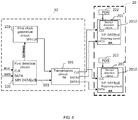
- the radio frequency front-end module 10 may include a first detection circuit 100, a first clock generation circuit 102, and a transmission circuit (a transmission circuit TX) 101.
- a first input interface and a second input interface of the first detection circuit 100 are respectively connected to output interfaces of a main control module (which are connected via an existing signal bus), and the first detection circuit 100 is connected to an input interface of the first clock generation circuit 102 via one or more clock enable buses.
- An output interface of the first clock generation circuit 102 is connected to a first input interface of the transmission circuit 101 (which are connected via an existing signal bus).
- An output interface of the first detection circuit 100 is connected to a second input interface of the transmission circuit 101.
- the main control module may be any main control chip, baseband chip, or the like with a control function.
- the first input interface and the second input interface of the first detection circuit 100 may be any serial communication apparatus, for example, an MIPI interface or a GIPO interface, as long as the interfaces can receive the system clock signal SCLK and the system data signal SDATA transmitted by the main control module.
- the system clock signal SCLK and the system data signal SDATA transmitted by the main control module is received, to determine whether the latest valid SIPI data (the valid control information matching each of the radio frequency devices 20) for each of radio frequency devices 20 is present.
- a first clock generation circuit 102 is controlled to generate a first clock signal (an SIPI clock signal) with a specific frequency for a transmission circuit 101 by enabling a clock signal and disabling the clock signal via a clock enable bus, and the latest valid SIPI data DATA_S is transmitted to the transmission circuit 101, so that the transmission circuit 101 extracts the valid SIPI data according to the first clock signal through sampling and then transmits the valid SIPI data to the radio frequency devices 20 according to a preset rule.
- the preset rule may be encoding, sorting, intercepting, encrypting the valid SIPI data, or the like.
- a first power-on reset (POR) circuit (not shown in the figure) may be disposed in the radio frequency front-end module 10.
- the first power-on reset circuit is connected to the transmission circuit 101 for generating a reset signal to reset the transmission circuit 101, so that the transmission circuit 101 can receive the valid SIPI data DATA_S after being reset.
- each of the radio frequency devices 20 include a second power-on reset (POR) circuit 202 and a receiving circuit (a receiving circuit RX) 201.
- the second power-on reset circuit 202 is connected to the receiving circuit 201 for generating a reset signal to reset the receiving circuit 201, so that the receiving circuit 201 can receive the valid SIPI data after being reset.
- first input interfaces of receiving circuit 201s in all of the radio frequency devices 20 are respectively connected to a first output interface of the transmission circuit 101 via the first signal bus SA
- second input interfaces of the receiving circuits 201 in all of the radio frequency devices 20 may be respectively connected to a second output interface of the transmission circuit 101 via the second signal bus SB.
- the second input interfaces of the receiving circuits 201 in all of the radio frequency devices 20 may be connected to a corresponding second output interface of the transmission circuit 101 via the second signal bus SB.
- the first input interfaces of the receiving circuits 201 in all of the radio frequency devices 20 are connected to a corresponding first output interface of the transmission circuit 101 via the first signal bus SA
- the second input interfaces of the receiving circuit 201s in all of the radio frequency devices 20 may be respectively connected to the corresponding second output interface of the transmission circuit 101 via the second signal bus SB.
- the receiving circuit 201 includes a second detection circuit 2010 configured to extract the valid SIPI data received by the receiving circuit 201 through sampling, to decode and configure (configuration of various functions) of the valid SIPI data, so that the radio frequency devices 20 can update the valid SIPI data synchronously in real time.
- a second detection circuit 2010 configured to extract the valid SIPI data received by the receiving circuit 201 through sampling, to decode and configure (configuration of various functions) of the valid SIPI data, so that the radio frequency devices 20 can update the valid SIPI data synchronously in real time.
- each of the radio frequency devices 20 include a second power-on reset (POR) circuit 202, a receiving circuit (a receiving circuit RX) 201, and a second clock generation circuit 203.
- the second power-on reset circuit 202 is connected to the receiving circuit 201 and has the same function as above, and therefore details are not described herein again.
- An output interface of the receiving circuit 201 is connected to an input interface of the second clock generation circuit 203 via one or more clock enable buses, and an output interface of the second clock generation circuit 203 is connected to an input interface of the receiving circuit 201 (which are connected via an existing signal bus).
- the receiving circuit 201 controls the second clock generation circuit 203 to generate a second clock signal CLK_i with a specific frequency by enabling and disabling the clock signal via the clock enable bus, and transmits the second clock signal to the receiving circuit 201.
- first input interfaces of receiving circuit 201s in all of the radio frequency devices 20 are respectively connected to the first output interface of the transmission circuit 101 via the first signal bus SA
- second input interfaces of receiving circuits 201 in all of the radio frequency devices 20 may be respectively connected to the second output interface of the transmission circuit 101 via the second signal bus SB.
- the second input interfaces of the receiving circuits 201 in all of the radio frequency devices 20 may be respectively connected to the corresponding second output interface of the transmission circuit 101 via the second signal bus SB.
- the receiving circuit 201 includes a second detection circuit 2010 configured to extract according to the second clock signal CLK_i through sampling, the valid SIPI data received by the receiving circuit 201, to decode and configure (configuration of various functions) of the valid SIPI data.
- the radio frequency device may be a power amplifier chip/module, a radio frequency switch, a radio frequency chip/module, or the like.
- the radio frequency front-end module 10 may include a first detection circuit 100, a first clock generation circuit 102, and a transmission circuit (a transmission circuit TX) 101.
- the radio frequency device 20 includes a second power-on reset (POR) circuit 202 and a receiving circuit (an SIPI receiving circuit RX) 201.
- the receiving circuit 201 includes a second detection circuit 2010.
- a first input interface and a second input interface of the first detection circuit 100 adopt MIPI interfaces.
- a connection relationship between parts of the SIPI provided in this embodiment is as follows.
- a first input interface CLOCK and a second input interface DATA of the first detection circuit 100 are respectively connected to the output interface of the main control module (which are connected via an existing signal bus).
- the first detection circuit 100 is connected to a corresponding input interface of the first clock generation circuit 102 via a clock enable bus CLK_ENABLE and a clock enable bus CLK_DISABLE, an output interface of the first clock generation circuit 102 is connected to a first input interface of the transmission circuit 101 via a signal bus 104, and an output interface of the first detection circuit 100 is connected to a second input interface of the transmission circuit 101 via a signal bus 103.
- a first output interface CLK of the transmission circuit 101 is connected to a first input interface CLK of the receiving circuit 201 via the first signal bus SA, a second output interface DATA of the transmission circuit 101 is connected to a second input interface DATA of the receiving circuit 201 via the second signal bus SB, and the receiving circuit 201 is connected to the second power-on reset circuit 202.
- the second power-on reset circuit 202 generates a reset signal to reset the receiving circuit 201, so that the reset receiving circuit 201 is to receive the valid SIPI data.
- a system clock signal SCLK and a system data signal SDATA transmitted by the main control module are received, and the received system clock signal SCLK and system data signal SDATA are detected and decoded in real time, and it may be determined whether the latest valid SIPI data (the valid control information matching each of the radio frequency devices 20) for the radio frequency device 20 exits through address information pre-stored in the first detection circuit 100 matching the radio frequency device 20.
- the clock signal is enabled and the clock signal is disabled respectively through the clock enable bus CLK_ENABLE and the clock enable bus CLK_DISABLE to control the first clock generation circuit 102 to generate a first clock signal (an SIPI clock signal) with a specific frequency for the transmission circuit 101, and the latest valid SIPI data DATA_S is transmitted to the transmission circuit 101, so that the transmission circuit 101 extracts the valid SIPI data according to the first clock signal through sampling and then transmits the valid SIPI data to the receiving circuit 201 through encoding, sorting, interception, encryption, or the like.
- the valid SIPI data received by the receiving circuit 201 includes a clock signal and a data signal.
- the first signal bus SA may be a clock bus for transmitting the clock signal
- the second signal bus SB may be a data bus for transmitting the data signal.
- valid SIPI data is extracted through sampling by the second detection circuit 2010 from the clock signal and the data signal received by the receiving circuit 201, and the valid SIPI data is decoded and configured (configuration of various functions), so that the radio frequency device 20 updates the valid SIPI data synchronously in real time.
- the second detection circuit 2010 may further determine whether the received clock signal and data signal match the current radio frequency device.
- the valid SIPI data required by the radio frequency device 20 may be split into a plurality of pieces of data, and the plurality of pieces of valid SIPI data are respectively received through a plurality of receiving circuits 201.
- a number of second output interfaces DATA of the transmission circuit 101 and a number of receiving circuits 201 are correspondingly increased.
- a plurality of second output interfaces DATA of the transmission circuit 101 are connected to corresponding second input interfaces DATA of the receiving circuits 201 via corresponding second signal buses SB, so that the plurality of pieces of valid SIPI data (the plurality of pieces of split valid SIPI data) are correspondingly transmitted to the plurality of receiving circuits 201 of the radio frequency device 20 efficiently and quickly via the plurality of second output interfaces DATA of the transmission circuit 101.
- the corresponding valid SIPI data is extracted through sampling by second detection circuits 2010 of the receiving circuits 201, and the extracted valid SIPI data is decoded and configured (configuration of various functions), thus enabling each of the radio frequency devices 20 to update the valid SIPI data synchronously in real time.
- each of the receiving circuits 201 needs to be connected to the second power-on reset circuit 202.
- the second power-on reset circuit 202 generates a reset signal to reset each of the receiving circuits 201, so that the reset receiving circuit 201 is to receive valid SIPI data.
- the number of second output interfaces of the transmission circuit 101 and the number of receiving circuits are respectively increased to two, that is, the second output interfaces of the transmission circuit 1011 are a second output interface DATA0 and a second output interface DATA1, and the receiving circuits are a receiving circuit 201' and a receiving circuit 201".
- the second output interface DATA0 is connected to a second input interface DATA of the receiving circuit 201' via the second signal bus SB
- the second output interface DATA1 is connected to a second input interface DATA of the receiving circuit 201" via the second signal bus SB.
- the first output interface CLK of the transmission circuit 101 is connected to first input interfaces CLK of the receiving circuit 201' and the receiving circuit 201" via the first signal bus SA.
- the second power-on reset circuit 202 generates reset signals to respectively reset the receiving circuit 201' and the receiving circuit 201", so that the reset receiving circuit 201' and the receiving circuit 201" are to receive valid SIPI data.
- the system clock signal SCLK and the system data signal SDATA transmitted by the main control module is received, and the received system clock signal SCLK and system data signal SDATA are detected and decoded in real time, and it may be determined whether the latest valid SIPI data DATA[x:0] for the radio frequency device 20 is present through address information pre-stored in the first detection circuit 100 matching the radio frequency device 20.
- the clock signal may be enabled and the clock signal may be disabled correspondingly through the clock enable bus CLK_ENABLE to control the first clock generation circuit 102 to generate a first clock signal (an SIPI clock signal) with a specific frequency for the transmission circuit 101, and the latest valid SIPI data DATA[x:0] is transmitted to the transmission circuit 101, so that the transmission circuit 101 extracts the valid SIPI data DATA[x:y] and the valid SIPI data DATA[y:0] according to the first clock signal through sampling, and then correspondingly transmits the valid SIPI data DATA[x:y] and the valid SIPI data DATA[y:0] to the receiving circuit 201' and the receiving circuit 201" through encoding, sorting, interception, encryption, or the like.
- the corresponding valid SIPI data is extracted through sampling by the second detection circuits 2010 of the receiving circuits, to decode and configure the extracted valid SIPI data (configuration of various functions), so that the
- the valid SIPI data may be sent to each of the radio frequency devices 20 through the first output interface and the second output interface of the transmission circuit 101.
- the first input interfaces of the receiving circuits 201 in all of the radio frequency devices 20 are respectively connected to the first output interface of the transmission circuit 101 via the first signal bus SA
- the second input interfaces of the receiving circuits 201 in all of the radio frequency devices 20 may be respectively connected to the second output interface of the transmission circuit 101 via the second signal bus SB.
- the second power-on reset circuit 202 generates reset signals to respectively reset the receiving circuits 201, so that the reset receiving circuits 201 are to receive the valid SIPI data.
- the system clock signal SCLK and the system data signal SDATA transmitted by the main control module are received, and the received system clock signal SCLK and system data signal SDATA are detected and decoded in real time, and it may be determined whether the latest valid SIPI data DATA[x:0] for the radio frequency device 20 is present through address information pre-stored in the first detection circuit 100 matching the radio frequency device 20.
- the clock signal is enabled and the clock signal is disabled correspondingly through the clock enable bus CLK_ENABLE to control the first clock generation circuit 102 to generate a first clock signal (an SIPI clock signal) with a specific frequency for the transmission circuit 101, and the latest valid SIPI data DATA[x:0] is transmitted to the transmission circuit 101, so that the transmission circuit 101 extracts the valid SIPI data DATA[x:0] according to the first clock signal through sampling, and then correspondingly transmits the valid SIPI data DATA[x:0] to the receiving circuits 201 through encoding, sorting, interception, encryption, or the like.
- the corresponding valid SIPI data DATA[x:0] is extracted through sampling by the second detection circuits 2010 of the receiving circuits, to decode and configure the extracted valid SIPI data[x:0] (configuration of various functions), so that the radio frequency device 20 updates the valid SIPI data synchronously in real time, which greatly simplifies complexity of serial communication apparatuses of all of the radio frequency devices 20 (the first input interfaces and the second input interfaces of all of the radio frequency devices).
- the valid SIPI data required by all of the radio frequency devices 20 may be randomly distributed in entire valid SIPI data in series.
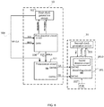
- the radio frequency front-end module 10 may include a first detection circuit 100, a first clock generation circuit 102, and a transmission circuit (an SIPI transmission circuit TX) 101.
- the radio frequency device 20 includes a second power-on reset (POR) circuit 202, a receiving circuit (an SIPI receiving circuit RX) 201, and a second clock generation circuit 203.
- the receiving circuit 201 includes a second detection circuit 2010.
- a first input interface and a second input interface of the first detection circuit 100 adopt MIPI interfaces.
- a connection relationship between parts of the SIPI provided in this embodiment is as follows.
- a first input interface CLOCK and a second input interface DATA of the first detection circuit 100 are correspondingly connected to the output interface of the main control module (which are connected via an existing signal bus).
- the first detection circuit 100 is connected to a corresponding input interface of the first clock generation circuit 102 via a clock enable bus CLK_ENABLE and a clock enable bus CLK_DISABLE, an output interface of the first clock generation circuit 102 is connected to a first input interface of the transmission circuit 101 via the signal bus 104, and an output interface of the first detection circuit 100 is connected to a second input interface of the transmission circuit 101 via the signal bus 103.
- a first output interface DATA0 of the transmission circuit 101 is connected to a first input interface DATA0 of the receiving circuit 201 via the first signal bus SA, a second output interface DATA1 of the transmission circuit 101 is connected to a second input interface DATA1 of the receiving circuit 201 via the second signal bus SB, and the receiving circuit 201 is connected to the second power-on reset circuit 202.
- the second power-on reset circuit 202 generates a reset signal to reset the receiving circuit 201, so that the reset receiving circuit 201 is to receive the valid SIPI data.
- a system clock signal SCLK and a system data signal SDATA transmitted by the main control module are received, and the received system clock signal SCLK and system data signal SDATA are detected and decoded in real time, and it may be determined whether latest valid SIPI data (valid control information matching each of the radio frequency devices 20) for the radio frequency device 20 exits through address information pre-stored in the first detection circuit 100 matching the radio frequency device 20.
- the first clock generation circuit 102 is controlled to generate a first clock signal (an SIPI clock signal) with a specific frequency for the transmission circuit 101 by enabling the clock signal and disabling the clock signal correspondingly through the clock enable bus CLK_ENABLE and the clock enable bus CLK_DISABLE, and the latest valid SIPI data DATA_S is transmitted to the transmission circuit 101, so that the transmission circuit 101 extracts the valid SIPI data according to the first clock signal through sampling and then transmits the valid SIPI data to the receiving circuit 201 through encoding, sorting, interception, encryption, or the like.
- the valid SIPI data received by the receiving circuit 201 includes only a data signal.
- the first signal bus SA may be a first data bus for transmitting the data signal
- the second signal bus SB may be a second data bus also for transmitting the data signal.
- the valid SIPI data can be sampled from the data signal transmitted via the first data bus and the data signal transmitted via the second data bus.
- the receiving circuit 201 may control, according to the received data frame header signal or data frame tail signal of the valid SIPI data, the second clock generation circuit 203 to generate a second clock signal CLK_i (an SIPI clock signal) with a specific frequency for the receiving circuit 201 by enabling the clock signal and disabling the clock signal correspondingly through the clock enable bus CLK_ENABLE and the clock enable bus CLK_DISABLE, so that the second detection circuit 2010 extracts the valid SIPI data according to the second clock signal through sampling, and then decodes and configures the valid SIPI data (configuration of various functions), thus enabling the radio frequency device 20 to update the valid SIPI data synchronously in real time.
- the second detection circuit 2010 may further determine whether the received data signal matches the current radio frequency device.
- the data frame header signal and the data frame tail signal are respectively used to determine positions of a start bit and a stop bit of the valid SIPI data.
- the second power-on reset circuit 202 generates reset signals to respectively reset the receiving circuits 201, so that the reset receiving circuits 201 are to receive valid SIPI data.
- a system clock signal SCLK and a system data signal SDATA transmitted by the main control module are received, and the received system clock signal SCLK and system data signal SDATA are detected and decoded in real time, and it may be determined whether latest valid SIPI data DATA[x:0] for the radio frequency device 20 is present through address information pre-stored in the first detection circuit 100 matching the radio frequency device 20.
- the first clock generation circuit 102 is controlled to generate a first clock signal (an SIPI clock signal) with a specific frequency for the transmission circuit 101 by enabling the clock signal and disabling the clock signal correspondingly through the clock enable bus CLK_ENABLE, and the latest valid SIPI data DATA[x:0] is transmitted to the transmission circuit 101, so that the transmission circuit 101 extracts the valid SIPI data DATA[x:0] according to the first clock signal through sampling and then transmits the valid SIPI data to DATA[x:0] to the receiving circuits 201 via two sets of data buses (a first data bus DATA0A and a second data bus DATA1A, and a first data bus DATA0B and a second data bus DATA1B) respectively through encoding, sorting, interception, encryption, or the like.
- a first clock signal an SIPI clock signal
- Each of the receiving circuits 201 may control, according to a received data frame header signal or data frame tail signal of the valid SIPI data, the second clock generation circuit 203 to generate a second clock signal CLK_i (an SIPI clock signal) with a specific frequency for the receiving circuit 201 by enabling the clock signal and disabling the clock signal correspondingly through the clock enable bus CLK_ENABLE and the clock enable bus CLK_DISABLE, so that the second detection circuit 2010 extracts the valid SIPI data according to the second clock signal through sampling, and then decodes and configures the valid SIPI data (configuration of various functions), thus enabling each of the radio frequency devices 20 to update the valid SIPI data synchronously in real time. In this case, use efficiency and transmission efficiency of the valid SIPI data may be higher, and more valid control information is transmitted.
- CLK_i an SIPI clock signal
- the transmission circuit 101 may adopt a unified dual output interface (a first output interface and a second output interface). For example, as shown in FIG. 10 , assuming that all valid SIPI data required by all of radio frequency devices 20 is data[x:0], the second power-on reset circuit 202 generates reset signals to respectively reset the receiving circuits 201, so that the reset receiving circuits 201 are to receive the valid SIPI data.
- the system clock signal SCLK and the system data signal SDATA transmitted by the main control module is received, and the received system clock signal SCLK and system data signal SDATA are detected and decoded in real time, and it may be determined whether the latest valid SIPI data DATA[x:0] for the radio frequency device 20 is present through address information pre-stored in the first detection circuit 100 matching the radio frequency device 20.
- the first clock generation circuit 102 is controlled to generate a first clock signal (an SIPI clock signal) with a specific frequency for the transmission circuit 101 by enabling the clock signal and disabling the clock signal correspondingly through the clock enable bus CLK_ENABLE, and the latest valid SIPI data DATA[x:0] is transmitted to the transmission circuit 101, so that the transmission circuit 101 extracts the valid SIPI data DATA[x:0] according to the first clock signal through sampling and then transmits the valid SIPI data to DATA[x:0] to the receiving circuits 201 via a first output interface DATA0 and a second output interface DATA1 respectively through encoding, sorting, interception, encryption, or the like.
- a first clock signal an SIPI clock signal
- Each of the receiving circuits 201 may control, according to a received data frame header signal or data frame tail signal of the valid SIPI data, the second clock generation circuit 203 to generate a second clock signal CLK_i (an SIPI clock signal) with a specific frequency for the receiving circuit 201 by enabling the clock signal and disabling the clock signal correspondingly through the clock enable bus CLK_ENABLE and the clock enable bus CLK_DISABLE, so that the second detection circuit 2010 extracts the valid SIPI data according to the second clock signal through sampling, and then decodes and configures the valid SIPI data (configuration of various functions), thus enabling each of the radio frequency devices 20 to update the valid SIPI data synchronously in real time.
- CLK_i an SIPI clock signal
- the valid SIPI data required by the radio frequency device 20 may be split into a plurality of pieces of data, and the plurality of pieces of valid SIPI data are respectively received through a plurality of receiving circuits 201.
- a number of first output interfaces DATA0 and second output interfaces DATA1 of the transmission circuit 101 and a number of receiving circuits 201 are correspondingly increased.
- a plurality of first output interfaces DATA0 of the transmission circuit 101 are connected to corresponding first input interfaces DATA0 of the receiving circuits 201 via corresponding first signal buses SA, and a plurality of second output interfaces DATA1 of the transmission circuit 101 are connected to corresponding second input interfaces DATA1 of the receiving circuits 201 via corresponding second signal buses SB, so that a plurality of pieces of valid SIPI data (a plurality of pieces of split valid SIPI data) is correspondingly transmitted to the plurality of receiving circuits 201 of the radio frequency device 20 efficiently and quickly via the plurality of first output interfaces DATA0 and second output interfaces DATA1 of the transmission circuit 101.
- Each of the receiving circuits 201 may control, according to a received data frame header signal or data frame tail signal of the valid SIPI data, the second clock generation circuit 203 to generate a second clock signal CLK_i (an SIPI clock signal) with a specific frequency for the receiving circuit 201 by enabling the clock signal and disabling the clock signal correspondingly through the clock enable bus CLK_ENABLE and the clock enable bus CLK_DISABLE, so that the second detection circuit 2010 extracts the valid SIPI data according to the second clock signal through sampling, and then decodes and configures the valid SIPI data (configuration of various functions), thus enabling each of the radio frequency devices 20 to update the valid SIPI data synchronously in real time.
- CLK_i an SIPI clock signal
- each of the receiving circuits 201 needs to be connected to the second power-on reset circuit 202.
- the second power-on reset circuit 202 generates a reset signal to reset each of the receiving circuits 201, so that the reset receiving circuit 201 is to receive valid SIPI data.
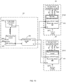
- the radio frequency front-end module 10 may include a first detection circuit 100, a first clock generation circuit 102, and a transmission circuit (a transmission circuit TX) 101.
- the radio frequency device 20 includes a second power-on reset (POR) circuit 202, a receiving circuit (an SIPI receiving circuit RX) 201, and a second clock generation circuit 203.
- the receiving circuit 201 includes a second detection circuit 2010.
- a first input interface and a second input interface of the first detection circuit 100 adopt MIPI interfaces.
- a connection relationship between parts of the SIPI provided in this embodiment is as follows.
- a first input interface CLOCK and a second input interface DATA of the first detection circuit 100 are correspondingly connected to the output interface of the main control module (which are connected via an existing signal bus).
- the first detection circuit 100 is connected to a corresponding input interface of the first clock generation circuit 102 via the clock enable bus CLK_ENABLE and the clock enable bus CLK_DISABLE, an output interface of the first clock generation circuit 102 is connected to a first input interface of the transmission circuit 101 via the signal bus 104, and an output interface of the first detection circuit 100 is connected to a second input interface of the transmission circuit 101 via the signal bus 103.
- a first output interface DATA of the transmission circuit 101 is connected to a first input interface DATA of the receiving circuit 201 via the first signal bus SA, a second output interface SE of the transmission circuit 101 is connected to a second input interface SE of the receiving circuit 201 via the second signal bus SB, and the receiving circuit 201 is connected to the second power-on reset circuit 202.
- the second power-on reset circuit 202 generates a reset signal to reset the receiving circuit 201, so that the reset receiving circuit 201 is to receive the valid SIPI data.
- a system clock signal SCLK and a system data signal SDATA transmitted by the main control module are received, and the received system clock signal SCLK and system data signal SDATA are detected and decoded in real time, and it may be determined whether latest valid SIPI data (valid control information matching each of the radio frequency devices 20) for the radio frequency device 20 is present through address information pre-stored in the first detection circuit 100 matching the radio frequency device 20.
- the first clock generation circuit 102 is controlled to generate a first clock signal (an SIPI clock signal) with a specific frequency for the transmission circuit 101 by enabling the clock signal and disabling the clock signal correspondingly through the clock enable bus CLK_ENABLE and the clock enable bus CLK_DISABLE, and the latest valid SIPI data DATA_S is transmitted to the transmission circuit 101, so that the transmission circuit 101 extracts the valid SIPI data according to the first clock signal through sampling and then transmits the valid SIPI data to the receiving circuit 201 through encoding, sorting, interception, encryption, or the like.
- the valid SIPI data received by the receiving circuit 201 includes a data signal and an enable signal.
- the first signal bus SA may be a data bus for transmitting the data signal
- the second signal bus SB may be an enable bus for transmitting the enable signal.
- the valid SIPI data can be sampled from the data signal transmitted via the data bus and the enable signal transmitted via the enable bus.
- the receiving circuit 201 may control, according to the received data frame header signal or data frame tail signal of the valid SIPI data, the second clock generation circuit 203 to generate a second clock signal CLK_i (an SIPI clock signal) with a specific frequency for the receiving circuit 201 by enabling the clock signal and disabling the clock signal correspondingly through the clock enable bus CLK_ENABLE and the clock enable bus CLK_DISABLE, so that the second detection circuit 2010 extracts the valid SIPI data according to the second clock signal through sampling, and then decodes and configures the valid SIPI data (configuration of various functions), thus enabling the radio frequency device 20 to update the valid SIPI data synchronously in real time.
- the second detection circuit 2010 may further determine whether the received data signal matches the current radio frequency device.
- the data frame header signal and the data frame tail signal are respectively used to determine positions of a start bit and a stop bit of the valid SIPI data.
- the valid SIPI data required by the radio frequency device 20 may be split into a plurality of pieces of data, and the plurality of pieces of valid SIPI data are respectively received through a plurality of receiving circuits 201.
- a number of second output interfaces SE of the transmission circuit 101 and a number of receiving circuits 201 are correspondingly increased.
- a plurality of second output interfaces SE of the transmission circuit 101 are connected to corresponding second input interfaces SE of the receiving circuits 201 via corresponding second signal buses SB, so that a plurality of pieces of valid SIPI data (a plurality of pieces of split valid SIPI data) can be respectively transmitted to the plurality of receiving circuits 201 of the radio frequency devices 20 efficiently and quickly via a plurality of second output interfaces SE of the transmission circuit 101.
- Each of the receiving circuits 201 may control, according to a received data frame header signal or data frame tail signal of the valid SIPI data, the second clock generation circuit 203 to generate a second clock signal CLK_i (an SIPI clock signal) with a specific frequency for the receiving circuit 201 by respectively enabling the clock signal and disabling the clock signal through the clock enable bus CLK_ENABLE and the clock enable bus CLK_DISABLE, so that the second detection circuit 2010 extracts the valid SIPI data according to the second clock signal through sampling and then decodes and configures the valid SIPI data (configuration of various functions), thus enabling the radio frequency device 20 to update the valid SIPI data synchronously in real time.
- CLK_i an SIPI clock signal
- each of the receiving circuits 201 needs to be connected to the second power-on reset circuit 202.
- the second power-on reset circuit 202 generates a reset signal to reset each of the receiving circuits 201, so that the reset receiving circuit 201 is to receive valid SIPI data.
- a number of the second output interfaces of the transmission circuit 101 and a number of the receiving circuits are respectively increased to two, that is, the second output interfaces of the transmission circuit 1011 are a second output interface SE0 and a second output interface SE1, and the receiving circuits are a receiving circuit 201' and a receiving circuit 201".
- the second output interface SE0 is connected to the second input interface SE0 of the receiving circuit 201' via the second signal bus SB
- the second output interface SE1 is connected to the second input interface SE1 of the receiving circuit 201" via the second signal bus SB
- the first output interface DATA of the transmission circuit 101 is connected to first input interfaces DATA of the receiving circuit 201' and the receiving circuit 201" via the first signal bus SA.
- the second power-on reset circuit 202 generates reset signals to respectively reset the receiving circuit 201' and the receiving circuit 201", so that the reset receiving circuit 201' and the receiving circuit 201" are to receive valid SIPI data.
- the system clock signal SCLK and the system data signal SDATA transmitted by the main control module is received, and the received system clock signal SCLK and system data signal SDATA are detected and decoded in real time, and it may be determined whether the latest valid SIPI data DATA[x:0] for the radio frequency device 20 is present through address information pre-stored in the first detection circuit 100 matching the radio frequency device 20.
- the first clock generation circuit 102 is controlled to generate a first clock signal (an SIPI clock signal) with a specific frequency for the transmission circuit 101 by enabling the clock signal and disabling the clock signal correspondingly through the clock enable bus CLK_ENABLE, and the latest valid SIPI data DATA[x:0] is transmitted to the transmission circuit 101, so that the transmission circuit 101 extracts the valid SIPI data DATA[x:y] and the valid SIPI data DATA[y:0] according to the first clock signal through sampling and then transmits the valid SIPI data to DATA[x:y] and the valid SIPI data DATA[y:0] to the receiving circuit 201' and the receiving circuit 201" respectively through encoding, sorting, interception, encryption, or the like.
- a first clock signal an SIPI clock signal
- the receiving circuit 201' and the receiving circuit 201" may control, according to a received data frame header signal or data frame tail signal of the valid SIPI data, the second clock generation circuit 203 to generate a second clock signal CLK_i (an SIPI clock signal) with a specific frequency for the receiving circuit 201' and the receiving circuit 201" by enabling the clock signal and disabling the clock signal correspondingly through the clock enable bus CLK_ENABLE and the clock enable bus CLK_DISABLE, so that the second detection circuit 2010 extracts the valid SIPI data according to the second clock signal through sampling, and then decodes and configures the valid SIPI data (configuration of various functions), thus enabling the radio frequency device 20 to update the valid SIPI data synchronously in real time.
- CLK_i an SIPI clock signal
- the transmission circuit 101 may adopt a unified dual output interface (a first output interface DATA and a second output interface SE).
- a first output interface DATA and a second output interface SE For example, as shown in FIG. 13 , assuming that all valid SIPI data required by all of radio frequency devices 20 is DATA[x:0], the second power-on reset circuit 202 generates reset signals to respectively reset the receiving circuits 201, so that the reset receiving circuits 201 are to receive the valid SIPI data.
- a system clock signal SCLK and a system data signal SDATA transmitted by the main control module are received, and the received system clock signal SCLK and system data signal SDATA are detected and decoded in real time, and it may be determined whether latest valid SIPI data DATA[x:0] for the radio frequency device 20 is present through address information pre-stored in the first detection circuit 100 matching the radio frequency device 20.
- the first clock generation circuit 102 is controlled to generate a first clock signal (an SIPI clock signal) with a specific frequency for the transmission circuit 101 by enabling the clock signal and disabling the clock signal correspondingly through the clock enable bus CLK_ENABLE, and the latest valid SIPI data DATA[x:0] is transmitted to the transmission circuit 101, so that the transmission circuit 101 extracts the valid SIPI data DATA[x:0] according to the first clock signal through sampling and then transmits the valid SIPI data to DATA[x:0] to the receiving circuits 201 via the first output interface DATA and the second output interface SE respectively through encoding, sorting, interception, encryption, or the like.
- a first clock signal an SIPI clock signal
- Each of the receiving circuits 201 may control, according to a received data frame header signal or data frame tail signal of the valid SIPI data, the second clock generation circuit 203 to generate a second clock signal CLK_i (an SIPI clock signal) with a specific frequency for the receiving circuit 201 by enabling the clock signal and disabling the clock signal respectively through the clock enable bus CLK_ENABLE and the clock enable bus CLK_DISABLE, so that the second detection circuit 2010 extracts the valid SIPI data according to the second clock signal through sampling, and then decodes and configures the valid SIPI data (configuration of various functions), thus enabling the radio frequency devices 20 to update the valid SIPI data synchronously in real time.
- CLK_i an SIPI clock signal
- the serial communication apparatus detects and extracts valid SIPI data required by each of the radio frequency devices via the radio frequency front-end module, and transmits the valid SIPI data to each of the radio frequency devices quickly and efficiently in a parallel or cascaded serial manner, which not only satisfies requirements for convenient and fast unidirectional communication between and inside various chips of the radio frequency front-end module, but also reduces communication complexity and increases transmission efficiency.
- the present invention further provides a serial communication method. As shown in FIG. 14 , the serial communication method includes the following steps.
- Step S1 A radio frequency front-end module determines whether latest valid SIPI data is present in a system clock signal and a system data signal.
- Step S2 Enable generation of a first clock signal in the presence of the latest valid SIPI data; or otherwise receive the system clock signal and the system data signal again.
- Step S3 The radio frequency front-end module samples and extracts valid SIPI data from the first clock signal, and transmits the valid SIPI data to each of radio frequency devices in parallel or in series according to a preset rule.
- Step S4 Decode and configure the valid SIPI data if the valid SIPI data received by each of the radio frequency devices contains a clock signal; or otherwise enable generation of a second clock signal, and extract the valid SIPI data from the second clock signal through sampling for decoding and configuration.
- the serial communication apparatus provided in the present invention may be used in a semiconductor device (for example, a radio frequency chip or a radio frequency module) for transmitting, to the semiconductor device, control information matching the semiconductor device or satisfy requirements for convenient and fast unidirectional communication between and inside the semiconductor devices.
- a semiconductor device for example, a radio frequency chip or a radio frequency module
- control information matching the semiconductor device or satisfy requirements for convenient and fast unidirectional communication between and inside the semiconductor devices.
Abstract
Description
- The present invention relates to a serial communication apparatus and a corresponding serial communication method.
- As applications in which a radio frequency front end (RF front end) is adopted becomes increasingly complex, a number of required chips such as power amplifiers, radio frequency switches, low-noise power amplifiers, and filters increases accordingly. In this case, a state of each chip of a radio frequency front-end module in an actual application needs to be switched through a respective control signal. For a chip that does not have too many states, a general purpose input output (GPIO) interface is commonly adopted in the prior art to control changes in the states of the chip through a combination of states of a high level "1" and a low level "0".
- However, as the complexity and functions of applications in which radio frequency front ends are adopted increase, each chip also has more and more functions, and it is impractical to further increase a number of GPIO control signal lines. Therefore, mobile industry processor interface (MIPI) interfaces have come into being in the field of mobile phones. However, with costs increasing with each passing day, adopting the MIPI interfaces for communication between chips within a radio frequency front-end module results in an increased complexity of the chips, thus reducing efficiency of internal communication.
- In view of disadvantages of the prior art, the primary technical problem to be resolved in the present invention is to provide a serial communication apparatus.
- Another technical problem to be resolved in the present invention is to provide a serial communication method.
- Still another technical problem to be resolved in the present invention is to provide a semiconductor device including the above serial communication apparatus.
- In order to achieve the objective, the present invention adopts the following technical solutions.
- According to a first aspect of embodiments of the present invention, a serial communication apparatus is provided, including a radio frequency front-end module and radio frequency devices, where a first input interface and a second input interface of the radio frequency front-end module are respectively connected to output interfaces of a main control module, and when a first output interface of the radio frequency front-end module is connected to a first input interface of at least one of the radio frequency devices via a first signal bus, a second output interface of the radio frequency front-end module is connected to a second input interface of the at least one of the radio frequency devices via a second signal bus.
- According to a second aspect of embodiments of the present invention, a serial communication apparatus is provided, including a radio frequency front-end module and radio frequency devices, where a first input interface and a second input interface of the radio frequency front-end module are respectively connected to output interfaces of a main control module, at least one first output interface of the radio frequency front-end module is connected to a first input interface of at least one of the radio frequency devices via a first signal bus, and at least one second output interface of the radio frequency front-end module is connected to a second input interface of the at least one of the radio frequency devices via a second signal bus.
- According to a third aspect of embodiments of the present invention, a serial communication apparatus is provided, including a radio frequency front-end module and radio frequency devices, where a first input interface and a second input interface of the radio frequency front-end module are respectively connected to output interfaces of a main control module, a first output interface of the radio frequency front-end module is connected to a first input interface of a first one of the radio frequency devices via a first signal bus, a second output interface of the radio frequency front-end module is connected to a second input interface of the first one of the radio frequency devices via a second signal bus, and starting from the first one of the radio frequency devices, the radio frequency devices are successively connected via the first signal bus and the second signal bus respectively.
- Preferably, the radio frequency front-end module includes a first detection circuit, a first clock generation circuit, and a transmission circuit, where a first input interface and a second input interface of the first detection circuit are respectively connected to the output interfaces of the main control module, the first detection circuit is connected to an input interface of the first clock generation circuit via one or more clock enable buses, an output interface of the first clock generation circuit is connected to a first input interface of the transmission circuit, and an output interface of the first detection circuit is connected to a second input interface of the transmission circuit.
- Preferably, the first input interface and the second input interface include but are not limited to MIPI interfaces or GIPO interfaces.
- Preferably, the radio frequency front-end module further includes a first power-on reset circuit, where the first power-on reset circuit is connected to the transmission circuit.
- Preferably, when valid SIPI data received by each of the radio frequency devices contains a clock signal, the radio frequency device includes a second power-on reset circuit and a receiving circuit, where the second power-on reset circuit is connected to the receiving circuit, and when a first input interface of the receiving circuit is connected to a first output interface of a transmission circuit via the first signal bus, a second input interface of the receiving circuit is connected to a second output interface of the transmission circuit via the second signal bus, or the second input interface of the receiving circuit is connected to a corresponding second output interface of the transmission circuit via the second signal bus.
- Preferably, when valid SIPI data received by each of the radio frequency devices contains a clock signal, the radio frequency device includes a second power-on reset circuit and a receiving circuit, where the second power-on reset circuit is connected to the receiving circuit, a first input interface of the receiving circuit is connected to a corresponding first output interface of a transmission circuit via the first signal bus, and a second input interface of the receiving circuit is connected to a corresponding second output interface of the transmission circuit via the second signal bus.
- Preferably, when valid SIPI data received by each of the radio frequency devices contains a clock signal, the radio frequency device includes a second power-on reset circuit and a receiving circuit, where the second power-on reset circuit is connected to the receiving circuit, a first input interface of the receiving circuit of the first one of the radio frequency devices is connected to a first output interface of a transmission circuit via the first signal bus, a second input interface of the receiving circuit of the first one of the radio frequency devices is connected to a second output interface of the transmission circuit via the second signal bus, and starting from the first one of the radio frequency devices, the receiving circuits of the radio frequency devices are successively connected via the first signal bus and the second signal bus respectively.
- Preferably, a number of second output interfaces of the transmission circuit and a number of receiving circuits of each of the radio frequency devices are adjusted according to a bit width of the valid SIPI data required by each of the radio frequency devices.
- Preferably, when valid SIPI data received by each of the radio frequency devices does not contain a clock signal, the radio frequency device includes a second power-on reset circuit, a receiving circuit, and a second clock generation circuit, where the second power-on reset circuit is connected to the receiving circuit, an output interface of the receiving circuit is connected to an input interface of the second clock generation circuit via one or more clock enable buses, an output interface of the second clock generation circuit is connected to an input interface of the receiving circuit, and when a first input interface of the receiving circuit is connected to a first output interface of a transmission circuit via the first signal bus, a second input interface of the receiving circuit is connected to a second output interface of the transmission circuit via the second signal bus, or the second input interface of the receiving circuit is connected to a corresponding second output interface of the transmission circuit via the second signal bus.
- Preferably, when valid SIPI data received by each of the radio frequency devices does not contain a clock signal, the radio frequency device includes a second power-on reset circuit, a receiving circuit, and a second clock generation circuit, where the second power-on reset circuit is connected to the receiving circuit, an output interface of the receiving circuit is connected to an input interface of the second clock generation circuit via one or more clock enable buses, an output interface of the second clock generation circuit is connected to an input interface of the receiving circuit, a first input interface of the receiving circuit is connected to a corresponding first output interface of a transmission circuit via the first signal bus, and a second input interface of the receiving circuit is connected to a corresponding second output interface of the transmission circuit via the second signal bus.
- Preferably, when valid SIPI data received by each of the radio frequency devices does not contain a clock signal, the radio frequency device includes a second power-on reset circuit, a receiving circuit, and a second clock generation circuit, where the second power-on reset circuit is connected to the receiving circuit, an output interface of the receiving circuit is connected to an input interface of the second clock generation circuit via one or more clock enable buses, an output interface of the second clock generation circuit is connected to an input interface of the receiving circuit, a first input interface of the receiving circuit of the first one of the radio frequency devices is connected to a first output interface of a transmission circuit via the first signal bus, a second input interface of the receiving circuit of the first one of the radio frequency devices is connected to a second output interface of the transmission circuit via the second signal bus, and starting from the first one of the radio frequency device, the receiving circuits of the radio frequency devices are successively connected via the first signal bus and the second signal bus respectively.
- Preferably, a number of first output interfaces and second output interfaces of the transmission circuit and a number of receiving circuits of each of the radio frequency devices are adjusted according to a bit width of the valid SIPI data required by each of the radio frequency devices.
- Preferably, a number of second output interfaces of the transmission circuit and a number of receiving circuits of each of the radio frequency devices are adjusted according to a bit width of the valid SIPI data required by each of the radio frequency devices.
- Preferably, the receiving circuit includes a second detection circuit configured to extract the valid SIPI data received by the receiving circuit through sampling and decode and configure the valid SIPI data.
- According to a fourth aspect of the embodiments of the present invention, a serial communication method is provided, including the steps of:
- determining, by a radio frequency front-end module, whether latest valid SIPI data is present in a system clock signal and a system data signal received;
- enabling generation of a first clock signal in the presence of the latest valid SIPI data; or otherwise receiving the system clock signal and the system data signal again;
- extracting, by the radio frequency front-end module, the valid SIPI data from the first clock signal, and transmitting the valid SIPI data to each of radio frequency devices in parallel or in series according to a preset rule; and
- decoding and configuring the valid SIPI data if the valid SIPI data received by each of the radio frequency devices contains a clock signal; or otherwise enabling generation of a second clock signal, and extracting the valid SIPI data from the second clock signal for decoding and configuration.
- According to a fifth aspect of the embodiments of the present invention, a semiconductor device is provided, where the semiconductor device includes the above serial communication apparatus.
- The serial communication apparatus provided in the present invention detects and extracts valid SIPI data required by each of the radio frequency devices via the radio frequency front-end module, and transmits the valid SIPI data to each of the radio frequency devices quickly and efficiently in a parallel or cascaded serial manner, which not only satisfies requirements for convenient and fast unidirectional communication between and inside various chips of the radio frequency front-end module, but also reduces communication complexity and increases transmission efficiency.
-
-
FIG. 1 is a schematic circuit diagram 1 of a serial communication apparatus according to the present invention; -
FIG. 2 is a schematic circuit diagram 2 of a serial communication apparatus according to the present invention; -
FIG. 3 is a schematic circuit diagram 3 of a serial communication apparatus according to the present invention; -
FIG. 4 is a schematic circuit diagram 4 of a serial communication apparatus according to the present invention; -
FIG. 5 is a schematic circuit diagram 1 of a serial communication apparatus according toEmbodiment 1 of the present invention; -
FIG. 6 is a schematic circuit diagram 2 of a serial communication apparatus according toEmbodiment 1 of the present invention; -
FIG. 7 is a schematic circuit diagram 3 of a serial communication apparatus according toEmbodiment 1 of the present invention; -
FIG. 8 is a schematic circuit diagram 1 of a serial communication apparatus according toEmbodiment 2 of the present invention; -
FIG. 9 is a schematic circuit diagram 2 of a serial communication apparatus according toEmbodiment 2 of the present invention; -
FIG. 10 is a schematic circuit diagram 3 of a serial communication apparatus according toEmbodiment 2 of the present invention; -
FIG. 11 is a schematic circuit diagram 1 of a serial communication apparatus according to Embodiment 3 of the present invention; -
FIG. 12 is a schematic circuit diagram 2 of a serial communication apparatus according to Embodiment 3 of the present invention; -
FIG. 13 is a schematic circuit diagram 3 of a serial communication apparatus according to Embodiment 3 of the present invention; -
FIG. 14 is a flowchart of a serial communication method according to the present invention. - Technical contents of the present invention are further described in detail below with reference to the accompanying drawings and specific embodiments.
- A serial communication apparatus provided in the present invention is configured to transmit, to chips of a radio frequency front-end radio frequency module, control information matching the chips, or to satisfy requirements for convenient and fast unidirectional communication between and inside the chips of the radio frequency front-end module. For convenience of description, the inventor refers to the serial communication apparatus as a scalable intra peripheral interface (SIPI). In embodiments of the present invention, the SIPI is used to directly refer to the serial communication apparatus provided in the present invention.
- As shown in
FIG. 1 and FIG. 2 , the SIPI includes a radio frequency front-end module 10 andradio frequency devices 20. A first input interface and a second input interface of the radio frequency front-end module 10 are respectively connected to an output interface of a main control module (which may be connected via an existing signal bus). When a first output interface of the radio frequency front-end module 10 is connected to a first input interface of the at least one of theradio frequency devices 20 via a first signal bus SA, a second output interface of the radio frequency front-end module 10 is connected to a second input interface of the at least one of theradio frequency devices 20 via a second signal bus SB. Alternatively, at least one second output interface of the radio frequency front-end module 10 is connected to a second input interface of the at least one of theradio frequency devices 20 via a second signal bus SB. - As shown in
FIG. 3 , in the SIPI, alternatively, at least one first input interface of the radio frequency front-end module 10 may be connected to the first input interface of the at least one of theradio frequency devices 20 via the first signal bus SA, and at least one second output interface of the radio frequency front-end module 10 is connected to the second input interface of the at least one of theradio frequency devices 20 via the second signal bus SB. A connection relationship between the first input interface and the second input interface of the radio frequency front-end module 10 is the same as above, and therefore details are not described herein again. - The radio frequency front-
end module 10 receives a system clock signal SCLK and a system data signal SDATA transmitted by the main control module, and determines whether latest valid SIPI data (valid control information matching each of the radio frequency devices 20) for each of theradio frequency devices 20 is present; enables generation of a first clock signal in the presence of the latest valid SIPI data for each of theradio frequency devices 20, or otherwise receives the system clock signal SCLK and the system data signal SDATA again; and extracts the valid SIPI data according to the first clock signal through sampling, and transmits the valid SIPI data to each of theradio frequency devices 20 in parallel according to a preset rule, to implement decoding and configuration of the valid SIPI data (configuration of various functions, such as current/voltage adjustment), so that theradio frequency devices 20 update the valid SIPI data synchronously in real time. - As shown in
FIG. 4 , in the SIPI, alternatively, a first output interface of the radio frequency front-end module 10 may be connected to a first input interface of a first one of theradio frequency device 20 via the first signal bus SA, a second output interface of the radio frequency front-end module 10 is connected to a second input interface of the firstradio frequency device 20 via the second signal bus SB, and starting from the first one of theradio frequency device 20, theradio frequency devices 20 are successively connected via the first signal bus SA and the second signal bus SB respectively (that is, adjacentradio frequency devices 20 are connected via the first signal bus SA and the second signal bus SB). A connection relationship between the first input interface and the second input interface of the radio frequency front-end module 10 is the same as above, and therefore details are not described herein again. - The radio frequency front-
end module 10 receives a system clock signal SCLK and a system data signal SDATA transmitted by the main control module, and determines whether the latest valid SIPI data (valid control information matching each of the radio frequency devices 20) for each of theradio frequency devices 20 is present; enables generation of a first clock signal in the presence of the latest valid SIPI data for each of theradio frequency devices 20, or otherwise receives the system clock signal SCLK and the system data signal SDATA again; and extracts the valid SIPI data according to the first clock signal through sampling, and transmits the valid SIPI data to theradio frequency devices 20 one by one (in a cascaded serial manner) according to a preset rule, to implement decoding and configuration of the valid SIPI data (configuration of various functions, such as current/voltage adjustment), so that theradio frequency devices 20 successively update the valid SIPI data synchronously in real time. - A structure and a principle of the SIPI are described in detail below with reference to
FIG. 5 to FIG. 13 by way of example that the radio frequency front-end module 10 transmits the latest valid SIP data to each of theradio frequency devices 20 in a parallel mode. A method for implementing unidirectional transmission of the valid SIPI data in a cascaded serial mode is easily obtained according to the method for implementing unidirectional transmission of the valid SIPI data in the parallel mode. In addition, a structure of a radio frequency front-end module 10 andradio frequency devices 20 of the SIPI in the cascaded serial mode is the same as a structure of a radio frequency front-end module 10 andradio frequency devices 20 of the SIPI in the parallel mode, and therefore details are not described herein again. - As shown in
FIG. 5 to FIG. 13 , in the SIPI, the radio frequency front-end module 10 may include afirst detection circuit 100, a firstclock generation circuit 102, and a transmission circuit (a transmission circuit TX) 101. A first input interface and a second input interface of thefirst detection circuit 100 are respectively connected to output interfaces of a main control module (which are connected via an existing signal bus), and thefirst detection circuit 100 is connected to an input interface of the firstclock generation circuit 102 via one or more clock enable buses. An output interface of the firstclock generation circuit 102 is connected to a first input interface of the transmission circuit 101 (which are connected via an existing signal bus). An output interface of thefirst detection circuit 100 is connected to a second input interface of thetransmission circuit 101. The main control module may be any main control chip, baseband chip, or the like with a control function. The first input interface and the second input interface of the first detection circuit 100 (that is, the first input interface and the second input interface of the radio frequency front-end module 10) may be any serial communication apparatus, for example, an MIPI interface or a GIPO interface, as long as the interfaces can receive the system clock signal SCLK and the system data signal SDATA transmitted by the main control module. - By means of the
first detection circuit 100, the system clock signal SCLK and the system data signal SDATA transmitted by the main control module is received, to determine whether the latest valid SIPI data (the valid control information matching each of the radio frequency devices 20) for each ofradio frequency devices 20 is present. In the presence of the latest valid SIPI data DATA_S for each of theradio frequency devices 20, a firstclock generation circuit 102 is controlled to generate a first clock signal (an SIPI clock signal) with a specific frequency for atransmission circuit 101 by enabling a clock signal and disabling the clock signal via a clock enable bus, and the latest valid SIPI data DATA_S is transmitted to thetransmission circuit 101, so that thetransmission circuit 101 extracts the valid SIPI data according to the first clock signal through sampling and then transmits the valid SIPI data to theradio frequency devices 20 according to a preset rule. The preset rule may be encoding, sorting, intercepting, encrypting the valid SIPI data, or the like. - In order to determine whether the
transmission circuit 101 of the radio frequency front-end module 10 is in a steady state to ensure accuracy of valid SIPI data DATA_S received by thetransmission circuit 101 each time, a first power-on reset (POR) circuit (not shown in the figure) may be disposed in the radio frequency front-end module 10. The first power-on reset circuit is connected to thetransmission circuit 101 for generating a reset signal to reset thetransmission circuit 101, so that thetransmission circuit 101 can receive the valid SIPI data DATA_S after being reset. - When the valid SIPI data received by the
radio frequency devices 20 contains a clock signal, each of theradio frequency devices 20 include a second power-on reset (POR)circuit 202 and a receiving circuit (a receiving circuit RX) 201. The second power-onreset circuit 202 is connected to the receivingcircuit 201 for generating a reset signal to reset the receivingcircuit 201, so that the receivingcircuit 201 can receive the valid SIPI data after being reset. When first input interfaces of receiving circuit 201s in all of theradio frequency devices 20 are respectively connected to a first output interface of thetransmission circuit 101 via the first signal bus SA, second input interfaces of the receivingcircuits 201 in all of theradio frequency devices 20 may be respectively connected to a second output interface of thetransmission circuit 101 via the second signal bus SB. Alternatively, the second input interfaces of the receivingcircuits 201 in all of theradio frequency devices 20 may be connected to a corresponding second output interface of thetransmission circuit 101 via the second signal bus SB. When the first input interfaces of the receivingcircuits 201 in all of theradio frequency devices 20 are connected to a corresponding first output interface of thetransmission circuit 101 via the first signal bus SA, the second input interfaces of the receiving circuit 201s in all of theradio frequency devices 20 may be respectively connected to the corresponding second output interface of thetransmission circuit 101 via the second signal bus SB. The receivingcircuit 201 includes asecond detection circuit 2010 configured to extract the valid SIPI data received by the receivingcircuit 201 through sampling, to decode and configure (configuration of various functions) of the valid SIPI data, so that theradio frequency devices 20 can update the valid SIPI data synchronously in real time. - When the valid SIPI data received by the
radio frequency devices 20 does not contain a clock signal, each of theradio frequency devices 20 include a second power-on reset (POR)circuit 202, a receiving circuit (a receiving circuit RX) 201, and a secondclock generation circuit 203. The second power-onreset circuit 202 is connected to the receivingcircuit 201 and has the same function as above, and therefore details are not described herein again. An output interface of the receivingcircuit 201 is connected to an input interface of the secondclock generation circuit 203 via one or more clock enable buses, and an output interface of the secondclock generation circuit 203 is connected to an input interface of the receiving circuit 201 (which are connected via an existing signal bus). After receiving the valid SIPI data, the receivingcircuit 201 controls the secondclock generation circuit 203 to generate a second clock signal CLK_i with a specific frequency by enabling and disabling the clock signal via the clock enable bus, and transmits the second clock signal to the receivingcircuit 201. When first input interfaces of receiving circuit 201s in all of theradio frequency devices 20 are respectively connected to the first output interface of thetransmission circuit 101 via the first signal bus SA, second input interfaces of receivingcircuits 201 in all of theradio frequency devices 20 may be respectively connected to the second output interface of thetransmission circuit 101 via the second signal bus SB. Alternatively, the second input interfaces of the receivingcircuits 201 in all of theradio frequency devices 20 may be respectively connected to the corresponding second output interface of thetransmission circuit 101 via the second signal bus SB. When the first input interfaces of the receivingcircuits 201 in all of theradio frequency devices 20 are respectively connected to the corresponding first output interface of thetransmission circuit 101 via the first signal bus SA, the second input interfaces of the receivingcircuits 201 in all of theradio frequency devices 20 may be respectively connected to the corresponding second output interface of thetransmission circuit 101 via the second signal bus SB. The receivingcircuit 201 includes asecond detection circuit 2010 configured to extract according to the second clock signal CLK_i through sampling, the valid SIPI data received by the receivingcircuit 201, to decode and configure (configuration of various functions) of the valid SIPI data. The radio frequency device may be a power amplifier chip/module, a radio frequency switch, a radio frequency chip/module, or the like. - The structure and the principle of the above SIPI are described in detail below with reference to
FIG. 5 to FIG. 16 , using situations in which theradio frequency device 20 including respectively one and two radio frequency devices as examples. - As shown in
FIG. 5 , in the SIPI provided in this embodiment, the radio frequency front-end module 10 may include afirst detection circuit 100, a firstclock generation circuit 102, and a transmission circuit (a transmission circuit TX) 101. Theradio frequency device 20 includes a second power-on reset (POR)circuit 202 and a receiving circuit (an SIPI receiving circuit RX) 201. The receivingcircuit 201 includes asecond detection circuit 2010. For example, a first input interface and a second input interface of thefirst detection circuit 100 adopt MIPI interfaces. A connection relationship between parts of the SIPI provided in this embodiment is as follows. A first input interface CLOCK and a second input interface DATA of thefirst detection circuit 100 are respectively connected to the output interface of the main control module (which are connected via an existing signal bus). Thefirst detection circuit 100 is connected to a corresponding input interface of the firstclock generation circuit 102 via a clock enable bus CLK_ENABLE and a clock enable bus CLK_DISABLE, an output interface of the firstclock generation circuit 102 is connected to a first input interface of thetransmission circuit 101 via asignal bus 104, and an output interface of thefirst detection circuit 100 is connected to a second input interface of thetransmission circuit 101 via asignal bus 103. A first output interface CLK of thetransmission circuit 101 is connected to a first input interface CLK of the receivingcircuit 201 via the first signal bus SA, a second output interface DATA of thetransmission circuit 101 is connected to a second input interface DATA of the receivingcircuit 201 via the second signal bus SB, and the receivingcircuit 201 is connected to the second power-onreset circuit 202. - The second power-on
reset circuit 202 generates a reset signal to reset the receivingcircuit 201, so that thereset receiving circuit 201 is to receive the valid SIPI data. In this case, by means of thefirst detection circuit 100, a system clock signal SCLK and a system data signal SDATA transmitted by the main control module are received, and the received system clock signal SCLK and system data signal SDATA are detected and decoded in real time, and it may be determined whether the latest valid SIPI data (the valid control information matching each of the radio frequency devices 20) for theradio frequency device 20 exits through address information pre-stored in thefirst detection circuit 100 matching theradio frequency device 20. In the presence of the latest valid SIPI data DATA_S for theradio frequency device 20, the clock signal is enabled and the clock signal is disabled respectively through the clock enable bus CLK_ENABLE and the clock enable bus CLK_DISABLE to control the firstclock generation circuit 102 to generate a first clock signal (an SIPI clock signal) with a specific frequency for thetransmission circuit 101, and the latest valid SIPI data DATA_S is transmitted to thetransmission circuit 101, so that thetransmission circuit 101 extracts the valid SIPI data according to the first clock signal through sampling and then transmits the valid SIPI data to the receivingcircuit 201 through encoding, sorting, interception, encryption, or the like. The valid SIPI data received by the receivingcircuit 201 includes a clock signal and a data signal. Therefore, the first signal bus SA may be a clock bus for transmitting the clock signal, and the second signal bus SB may be a data bus for transmitting the data signal. In addition, valid SIPI data is extracted through sampling by thesecond detection circuit 2010 from the clock signal and the data signal received by the receivingcircuit 201, and the valid SIPI data is decoded and configured (configuration of various functions), so that theradio frequency device 20 updates the valid SIPI data synchronously in real time. Thesecond detection circuit 2010 may further determine whether the received clock signal and data signal match the current radio frequency device. - When a bit width of valid SIPI data required by the
radio frequency device 20 in this embodiment is relatively large, the valid SIPI data required by theradio frequency device 20 may be split into a plurality of pieces of data, and the plurality of pieces of valid SIPI data are respectively received through a plurality of receivingcircuits 201. In other words, a number of second output interfaces DATA of thetransmission circuit 101 and a number of receivingcircuits 201 are correspondingly increased. A plurality of second output interfaces DATA of thetransmission circuit 101 are connected to corresponding second input interfaces DATA of the receivingcircuits 201 via corresponding second signal buses SB, so that the plurality of pieces of valid SIPI data (the plurality of pieces of split valid SIPI data) are correspondingly transmitted to the plurality of receivingcircuits 201 of theradio frequency device 20 efficiently and quickly via the plurality of second output interfaces DATA of thetransmission circuit 101. The corresponding valid SIPI data is extracted through sampling bysecond detection circuits 2010 of the receivingcircuits 201, and the extracted valid SIPI data is decoded and configured (configuration of various functions), thus enabling each of theradio frequency devices 20 to update the valid SIPI data synchronously in real time. It is to be emphasized that each of the receivingcircuits 201 needs to be connected to the second power-onreset circuit 202. The second power-onreset circuit 202 generates a reset signal to reset each of the receivingcircuits 201, so that thereset receiving circuit 201 is to receive valid SIPI data. - For example, as shown in
FIG. 6 , assuming that valid SIPI data DATA[x:0] required by theradio frequency device 20 is split into valid SIPI data DATA[x:y] and valid SIPI data DATA[y:0], the number of second output interfaces of thetransmission circuit 101 and the number of receiving circuits are respectively increased to two, that is, the second output interfaces of the transmission circuit 1011 are a second output interface DATA0 and a second output interface DATA1, and the receiving circuits are a receiving circuit 201' and a receivingcircuit 201". The second output interface DATA0 is connected to a second input interface DATA of the receiving circuit 201' via the second signal bus SB, and the second output interface DATA1 is connected to a second input interface DATA of the receivingcircuit 201" via the second signal bus SB. The first output interface CLK of thetransmission circuit 101 is connected to first input interfaces CLK of the receiving circuit 201' and the receivingcircuit 201" via the first signal bus SA. - The second power-on
reset circuit 202 generates reset signals to respectively reset the receiving circuit 201' and the receivingcircuit 201", so that the reset receiving circuit 201' and the receivingcircuit 201" are to receive valid SIPI data. In this case, by means of thefirst detection circuit 100, the system clock signal SCLK and the system data signal SDATA transmitted by the main control module is received, and the received system clock signal SCLK and system data signal SDATA are detected and decoded in real time, and it may be determined whether the latest valid SIPI data DATA[x:0] for theradio frequency device 20 is present through address information pre-stored in thefirst detection circuit 100 matching theradio frequency device 20. In the presence of the latest valid SIPI data DATA[x:0] for theradio frequency device 20, the clock signal may be enabled and the clock signal may be disabled correspondingly through the clock enable bus CLK_ENABLE to control the firstclock generation circuit 102 to generate a first clock signal (an SIPI clock signal) with a specific frequency for thetransmission circuit 101, and the latest valid SIPI data DATA[x:0] is transmitted to thetransmission circuit 101, so that thetransmission circuit 101 extracts the valid SIPI data DATA[x:y] and the valid SIPI data DATA[y:0] according to the first clock signal through sampling, and then correspondingly transmits the valid SIPI data DATA[x:y] and the valid SIPI data DATA[y:0] to the receiving circuit 201' and the receivingcircuit 201" through encoding, sorting, interception, encryption, or the like. The corresponding valid SIPI data is extracted through sampling by thesecond detection circuits 2010 of the receiving circuits, to decode and configure the extracted valid SIPI data (configuration of various functions), so that theradio frequency device 20 updates the valid SIPI data synchronously in real time. - When the bit width of the valid SIPI data required by the
radio frequency device 20 in this embodiment is not large, the valid SIPI data may be sent to each of theradio frequency devices 20 through the first output interface and the second output interface of thetransmission circuit 101. In other words, the first input interfaces of the receivingcircuits 201 in all of theradio frequency devices 20 are respectively connected to the first output interface of thetransmission circuit 101 via the first signal bus SA, and the second input interfaces of the receivingcircuits 201 in all of theradio frequency devices 20 may be respectively connected to the second output interface of thetransmission circuit 101 via the second signal bus SB. - For example, as shown in
FIG. 7 , assuming that all valid SIPI data required by all ofradio frequency devices 20 is DATA[x:0], the second power-onreset circuit 202 generates reset signals to respectively reset the receivingcircuits 201, so that thereset receiving circuits 201 are to receive the valid SIPI data. In this case, by means of thefirst detection circuit 100, the system clock signal SCLK and the system data signal SDATA transmitted by the main control module are received, and the received system clock signal SCLK and system data signal SDATA are detected and decoded in real time, and it may be determined whether the latest valid SIPI data DATA[x:0] for theradio frequency device 20 is present through address information pre-stored in thefirst detection circuit 100 matching theradio frequency device 20. In the presence of the latest valid SIPI data DATA[x:0] for theradio frequency device 20, the clock signal is enabled and the clock signal is disabled correspondingly through the clock enable bus CLK_ENABLE to control the firstclock generation circuit 102 to generate a first clock signal (an SIPI clock signal) with a specific frequency for thetransmission circuit 101, and the latest valid SIPI data DATA[x:0] is transmitted to thetransmission circuit 101, so that thetransmission circuit 101 extracts the valid SIPI data DATA[x:0] according to the first clock signal through sampling, and then correspondingly transmits the valid SIPI data DATA[x:0] to the receivingcircuits 201 through encoding, sorting, interception, encryption, or the like. The corresponding valid SIPI data DATA[x:0] is extracted through sampling by thesecond detection circuits 2010 of the receiving circuits, to decode and configure the extracted valid SIPI data[x:0] (configuration of various functions), so that theradio frequency device 20 updates the valid SIPI data synchronously in real time, which greatly simplifies complexity of serial communication apparatuses of all of the radio frequency devices 20 (the first input interfaces and the second input interfaces of all of the radio frequency devices). The valid SIPI data required by all of theradio frequency devices 20 may be randomly distributed in entire valid SIPI data in series. - As shown in
FIG. 8 , in the SIPI provided in this embodiment, the radio frequency front-end module 10 may include afirst detection circuit 100, a firstclock generation circuit 102, and a transmission circuit (an SIPI transmission circuit TX) 101. Theradio frequency device 20 includes a second power-on reset (POR)circuit 202, a receiving circuit (an SIPI receiving circuit RX) 201, and a secondclock generation circuit 203. The receivingcircuit 201 includes asecond detection circuit 2010. For example, a first input interface and a second input interface of thefirst detection circuit 100 adopt MIPI interfaces. A connection relationship between parts of the SIPI provided in this embodiment is as follows. A first input interface CLOCK and a second input interface DATA of thefirst detection circuit 100 are correspondingly connected to the output interface of the main control module (which are connected via an existing signal bus). Thefirst detection circuit 100 is connected to a corresponding input interface of the firstclock generation circuit 102 via a clock enable bus CLK_ENABLE and a clock enable bus CLK_DISABLE, an output interface of the firstclock generation circuit 102 is connected to a first input interface of thetransmission circuit 101 via thesignal bus 104, and an output interface of thefirst detection circuit 100 is connected to a second input interface of thetransmission circuit 101 via thesignal bus 103. A first output interface DATA0 of thetransmission circuit 101 is connected to a first input interface DATA0 of the receivingcircuit 201 via the first signal bus SA, a second output interface DATA1 of thetransmission circuit 101 is connected to a second input interface DATA1 of the receivingcircuit 201 via the second signal bus SB, and the receivingcircuit 201 is connected to the second power-onreset circuit 202. - The second power-on
reset circuit 202 generates a reset signal to reset the receivingcircuit 201, so that thereset receiving circuit 201 is to receive the valid SIPI data. In this case, by means of thefirst detection circuit 100, a system clock signal SCLK and a system data signal SDATA transmitted by the main control module are received, and the received system clock signal SCLK and system data signal SDATA are detected and decoded in real time, and it may be determined whether latest valid SIPI data (valid control information matching each of the radio frequency devices 20) for theradio frequency device 20 exits through address information pre-stored in thefirst detection circuit 100 matching theradio frequency device 20. In the presence of the latest valid SIPI data DATA_S for theradio frequency device 20, the firstclock generation circuit 102 is controlled to generate a first clock signal (an SIPI clock signal) with a specific frequency for thetransmission circuit 101 by enabling the clock signal and disabling the clock signal correspondingly through the clock enable bus CLK_ENABLE and the clock enable bus CLK_DISABLE, and the latest valid SIPI data DATA_S is transmitted to thetransmission circuit 101, so that thetransmission circuit 101 extracts the valid SIPI data according to the first clock signal through sampling and then transmits the valid SIPI data to the receivingcircuit 201 through encoding, sorting, interception, encryption, or the like. The valid SIPI data received by the receivingcircuit 201 includes only a data signal. Therefore, the first signal bus SA may be a first data bus for transmitting the data signal, and the second signal bus SB may be a second data bus also for transmitting the data signal. In addition, the valid SIPI data can be sampled from the data signal transmitted via the first data bus and the data signal transmitted via the second data bus. Since the valid SIPI data includes a data frame header signal, a data signal, and a data frame tail signal, the receivingcircuit 201 may control, according to the received data frame header signal or data frame tail signal of the valid SIPI data, the secondclock generation circuit 203 to generate a second clock signal CLK_i (an SIPI clock signal) with a specific frequency for the receivingcircuit 201 by enabling the clock signal and disabling the clock signal correspondingly through the clock enable bus CLK_ENABLE and the clock enable bus CLK_DISABLE, so that thesecond detection circuit 2010 extracts the valid SIPI data according to the second clock signal through sampling, and then decodes and configures the valid SIPI data (configuration of various functions), thus enabling theradio frequency device 20 to update the valid SIPI data synchronously in real time. Thesecond detection circuit 2010 may further determine whether the received data signal matches the current radio frequency device. The data frame header signal and the data frame tail signal are respectively used to determine positions of a start bit and a stop bit of the valid SIPI data. - As shown in
FIG. 9 , assuming that all of the valid SIPI data required by all of theradio frequency devices 20 is data[x:0], the second power-onreset circuit 202 generates reset signals to respectively reset the receivingcircuits 201, so that thereset receiving circuits 201 are to receive valid SIPI data. In this case, by means of thefirst detection circuit 100, a system clock signal SCLK and a system data signal SDATA transmitted by the main control module are received, and the received system clock signal SCLK and system data signal SDATA are detected and decoded in real time, and it may be determined whether latest valid SIPI data DATA[x:0] for theradio frequency device 20 is present through address information pre-stored in thefirst detection circuit 100 matching theradio frequency device 20. In the presence of the latest valid SIPI data DATA[x:0] for theradio frequency device 20, the firstclock generation circuit 102 is controlled to generate a first clock signal (an SIPI clock signal) with a specific frequency for thetransmission circuit 101 by enabling the clock signal and disabling the clock signal correspondingly through the clock enable bus CLK_ENABLE, and the latest valid SIPI data DATA[x:0] is transmitted to thetransmission circuit 101, so that thetransmission circuit 101 extracts the valid SIPI data DATA[x:0] according to the first clock signal through sampling and then transmits the valid SIPI data to DATA[x:0] to the receivingcircuits 201 via two sets of data buses (a first data bus DATA0A and a second data bus DATA1A, and a first data bus DATA0B and a second data bus DATA1B) respectively through encoding, sorting, interception, encryption, or the like. Each of the receivingcircuits 201 may control, according to a received data frame header signal or data frame tail signal of the valid SIPI data, the secondclock generation circuit 203 to generate a second clock signal CLK_i (an SIPI clock signal) with a specific frequency for the receivingcircuit 201 by enabling the clock signal and disabling the clock signal correspondingly through the clock enable bus CLK_ENABLE and the clock enable bus CLK_DISABLE, so that thesecond detection circuit 2010 extracts the valid SIPI data according to the second clock signal through sampling, and then decodes and configures the valid SIPI data (configuration of various functions), thus enabling each of theradio frequency devices 20 to update the valid SIPI data synchronously in real time. In this case, use efficiency and transmission efficiency of the valid SIPI data may be higher, and more valid control information is transmitted. - In addition, in order to simplify complexity of the communication between the radio frequency front-
end module 10 and theradio frequency devices 20 and to transmit more valid SIPI data to the radio frequency devices at higher transmission efficiency, thetransmission circuit 101 may adopt a unified dual output interface (a first output interface and a second output interface). For example, as shown inFIG. 10 , assuming that all valid SIPI data required by all ofradio frequency devices 20 is data[x:0], the second power-onreset circuit 202 generates reset signals to respectively reset the receivingcircuits 201, so that thereset receiving circuits 201 are to receive the valid SIPI data. In this case, by means of thefirst detection circuit 100, the system clock signal SCLK and the system data signal SDATA transmitted by the main control module is received, and the received system clock signal SCLK and system data signal SDATA are detected and decoded in real time, and it may be determined whether the latest valid SIPI data DATA[x:0] for theradio frequency device 20 is present through address information pre-stored in thefirst detection circuit 100 matching theradio frequency device 20. In the presence of the latest valid SIPI data DATA[x:0] for theradio frequency device 20, the firstclock generation circuit 102 is controlled to generate a first clock signal (an SIPI clock signal) with a specific frequency for thetransmission circuit 101 by enabling the clock signal and disabling the clock signal correspondingly through the clock enable bus CLK_ENABLE, and the latest valid SIPI data DATA[x:0] is transmitted to thetransmission circuit 101, so that thetransmission circuit 101 extracts the valid SIPI data DATA[x:0] according to the first clock signal through sampling and then transmits the valid SIPI data to DATA[x:0] to the receivingcircuits 201 via a first output interface DATA0 and a second output interface DATA1 respectively through encoding, sorting, interception, encryption, or the like. Each of the receivingcircuits 201 may control, according to a received data frame header signal or data frame tail signal of the valid SIPI data, the secondclock generation circuit 203 to generate a second clock signal CLK_i (an SIPI clock signal) with a specific frequency for the receivingcircuit 201 by enabling the clock signal and disabling the clock signal correspondingly through the clock enable bus CLK_ENABLE and the clock enable bus CLK_DISABLE, so that thesecond detection circuit 2010 extracts the valid SIPI data according to the second clock signal through sampling, and then decodes and configures the valid SIPI data (configuration of various functions), thus enabling each of theradio frequency devices 20 to update the valid SIPI data synchronously in real time. - When a bit width of valid SIPI data required by the
radio frequency device 20 in this embodiment is relatively large, the valid SIPI data required by theradio frequency device 20 may be split into a plurality of pieces of data, and the plurality of pieces of valid SIPI data are respectively received through a plurality of receivingcircuits 201. In other words, a number of first output interfaces DATA0 and second output interfaces DATA1 of thetransmission circuit 101 and a number of receivingcircuits 201 are correspondingly increased. A plurality of first output interfaces DATA0 of thetransmission circuit 101 are connected to corresponding first input interfaces DATA0 of the receivingcircuits 201 via corresponding first signal buses SA, and a plurality of second output interfaces DATA1 of thetransmission circuit 101 are connected to corresponding second input interfaces DATA1 of the receivingcircuits 201 via corresponding second signal buses SB, so that a plurality of pieces of valid SIPI data (a plurality of pieces of split valid SIPI data) is correspondingly transmitted to the plurality of receivingcircuits 201 of theradio frequency device 20 efficiently and quickly via the plurality of first output interfaces DATA0 and second output interfaces DATA1 of thetransmission circuit 101. Each of the receivingcircuits 201 may control, according to a received data frame header signal or data frame tail signal of the valid SIPI data, the secondclock generation circuit 203 to generate a second clock signal CLK_i (an SIPI clock signal) with a specific frequency for the receivingcircuit 201 by enabling the clock signal and disabling the clock signal correspondingly through the clock enable bus CLK_ENABLE and the clock enable bus CLK_DISABLE, so that thesecond detection circuit 2010 extracts the valid SIPI data according to the second clock signal through sampling, and then decodes and configures the valid SIPI data (configuration of various functions), thus enabling each of theradio frequency devices 20 to update the valid SIPI data synchronously in real time. It is to be emphasized that each of the receivingcircuits 201 needs to be connected to the second power-onreset circuit 202. The second power-onreset circuit 202 generates a reset signal to reset each of the receivingcircuits 201, so that thereset receiving circuit 201 is to receive valid SIPI data. - As shown in
FIG. 11 , in the SIPI provided in this embodiment, the radio frequency front-end module 10 may include afirst detection circuit 100, a firstclock generation circuit 102, and a transmission circuit (a transmission circuit TX) 101. Theradio frequency device 20 includes a second power-on reset (POR)circuit 202, a receiving circuit (an SIPI receiving circuit RX) 201, and a secondclock generation circuit 203. The receivingcircuit 201 includes asecond detection circuit 2010. For example, a first input interface and a second input interface of thefirst detection circuit 100 adopt MIPI interfaces. A connection relationship between parts of the SIPI provided in this embodiment is as follows. A first input interface CLOCK and a second input interface DATA of thefirst detection circuit 100 are correspondingly connected to the output interface of the main control module (which are connected via an existing signal bus). Thefirst detection circuit 100 is connected to a corresponding input interface of the firstclock generation circuit 102 via the clock enable bus CLK_ENABLE and the clock enable bus CLK_DISABLE, an output interface of the firstclock generation circuit 102 is connected to a first input interface of thetransmission circuit 101 via thesignal bus 104, and an output interface of thefirst detection circuit 100 is connected to a second input interface of thetransmission circuit 101 via thesignal bus 103. A first output interface DATA of thetransmission circuit 101 is connected to a first input interface DATA of the receivingcircuit 201 via the first signal bus SA, a second output interface SE of thetransmission circuit 101 is connected to a second input interface SE of the receivingcircuit 201 via the second signal bus SB, and the receivingcircuit 201 is connected to the second power-onreset circuit 202. - The second power-on
reset circuit 202 generates a reset signal to reset the receivingcircuit 201, so that thereset receiving circuit 201 is to receive the valid SIPI data. In this case, by means of thefirst detection circuit 100, a system clock signal SCLK and a system data signal SDATA transmitted by the main control module are received, and the received system clock signal SCLK and system data signal SDATA are detected and decoded in real time, and it may be determined whether latest valid SIPI data (valid control information matching each of the radio frequency devices 20) for theradio frequency device 20 is present through address information pre-stored in thefirst detection circuit 100 matching theradio frequency device 20. In the presence of the latest valid SIPI data DATA_S for theradio frequency device 20, the firstclock generation circuit 102 is controlled to generate a first clock signal (an SIPI clock signal) with a specific frequency for thetransmission circuit 101 by enabling the clock signal and disabling the clock signal correspondingly through the clock enable bus CLK_ENABLE and the clock enable bus CLK_DISABLE, and the latest valid SIPI data DATA_S is transmitted to thetransmission circuit 101, so that thetransmission circuit 101 extracts the valid SIPI data according to the first clock signal through sampling and then transmits the valid SIPI data to the receivingcircuit 201 through encoding, sorting, interception, encryption, or the like. The valid SIPI data received by the receivingcircuit 201 includes a data signal and an enable signal. Therefore, the first signal bus SA may be a data bus for transmitting the data signal, and the second signal bus SB may be an enable bus for transmitting the enable signal. In addition, the valid SIPI data can be sampled from the data signal transmitted via the data bus and the enable signal transmitted via the enable bus. Since the valid SIPI data includes a data frame header signal, a data signal, and a data frame tail signal, the receivingcircuit 201 may control, according to the received data frame header signal or data frame tail signal of the valid SIPI data, the secondclock generation circuit 203 to generate a second clock signal CLK_i (an SIPI clock signal) with a specific frequency for the receivingcircuit 201 by enabling the clock signal and disabling the clock signal correspondingly through the clock enable bus CLK_ENABLE and the clock enable bus CLK_DISABLE, so that thesecond detection circuit 2010 extracts the valid SIPI data according to the second clock signal through sampling, and then decodes and configures the valid SIPI data (configuration of various functions), thus enabling theradio frequency device 20 to update the valid SIPI data synchronously in real time. Thesecond detection circuit 2010 may further determine whether the received data signal matches the current radio frequency device. The data frame header signal and the data frame tail signal are respectively used to determine positions of a start bit and a stop bit of the valid SIPI data. - When a bit width of valid SIPI data required by the
radio frequency device 20 in this embodiment is relatively large, the valid SIPI data required by theradio frequency device 20 may be split into a plurality of pieces of data, and the plurality of pieces of valid SIPI data are respectively received through a plurality of receivingcircuits 201. In other words, a number of second output interfaces SE of thetransmission circuit 101 and a number of receivingcircuits 201 are correspondingly increased. A plurality of second output interfaces SE of thetransmission circuit 101 are connected to corresponding second input interfaces SE of the receivingcircuits 201 via corresponding second signal buses SB, so that a plurality of pieces of valid SIPI data (a plurality of pieces of split valid SIPI data) can be respectively transmitted to the plurality of receivingcircuits 201 of theradio frequency devices 20 efficiently and quickly via a plurality of second output interfaces SE of thetransmission circuit 101. Each of the receivingcircuits 201 may control, according to a received data frame header signal or data frame tail signal of the valid SIPI data, the secondclock generation circuit 203 to generate a second clock signal CLK_i (an SIPI clock signal) with a specific frequency for the receivingcircuit 201 by respectively enabling the clock signal and disabling the clock signal through the clock enable bus CLK_ENABLE and the clock enable bus CLK_DISABLE, so that thesecond detection circuit 2010 extracts the valid SIPI data according to the second clock signal through sampling and then decodes and configures the valid SIPI data (configuration of various functions), thus enabling theradio frequency device 20 to update the valid SIPI data synchronously in real time. It is to be emphasized that each of the receivingcircuits 201 needs to be connected to the second power-onreset circuit 202. The second power-onreset circuit 202 generates a reset signal to reset each of the receivingcircuits 201, so that thereset receiving circuit 201 is to receive valid SIPI data. - For example, as shown in
FIG. 12 , assuming that valid SIPI data DATA[x:0] required by theradio frequency device 20 is split into valid SIPI data DATA[x:y] and valid SIPI data DATA[y:0], a number of the second output interfaces of thetransmission circuit 101 and a number of the receiving circuits are respectively increased to two, that is, the second output interfaces of the transmission circuit 1011 are a second output interface SE0 and a second output interface SE1, and the receiving circuits are a receiving circuit 201' and a receivingcircuit 201". The second output interface SE0 is connected to the second input interface SE0 of the receiving circuit 201' via the second signal bus SB, the second output interface SE1 is connected to the second input interface SE1 of the receivingcircuit 201" via the second signal bus SB, and the first output interface DATA of thetransmission circuit 101 is connected to first input interfaces DATA of the receiving circuit 201' and the receivingcircuit 201" via the first signal bus SA. - The second power-on
reset circuit 202 generates reset signals to respectively reset the receiving circuit 201' and the receivingcircuit 201", so that the reset receiving circuit 201' and the receivingcircuit 201" are to receive valid SIPI data. In this case, by means of thefirst detection circuit 100, the system clock signal SCLK and the system data signal SDATA transmitted by the main control module is received, and the received system clock signal SCLK and system data signal SDATA are detected and decoded in real time, and it may be determined whether the latest valid SIPI data DATA[x:0] for theradio frequency device 20 is present through address information pre-stored in thefirst detection circuit 100 matching theradio frequency device 20. In the presence of the latest valid SIPI data DATA[x:0] for theradio frequency device 20, the firstclock generation circuit 102 is controlled to generate a first clock signal (an SIPI clock signal) with a specific frequency for thetransmission circuit 101 by enabling the clock signal and disabling the clock signal correspondingly through the clock enable bus CLK_ENABLE, and the latest valid SIPI data DATA[x:0] is transmitted to thetransmission circuit 101, so that thetransmission circuit 101 extracts the valid SIPI data DATA[x:y] and the valid SIPI data DATA[y:0] according to the first clock signal through sampling and then transmits the valid SIPI data to DATA[x:y] and the valid SIPI data DATA[y:0] to the receiving circuit 201' and the receivingcircuit 201" respectively through encoding, sorting, interception, encryption, or the like. The receiving circuit 201' and the receivingcircuit 201" may control, according to a received data frame header signal or data frame tail signal of the valid SIPI data, the secondclock generation circuit 203 to generate a second clock signal CLK_i (an SIPI clock signal) with a specific frequency for the receiving circuit 201' and the receivingcircuit 201" by enabling the clock signal and disabling the clock signal correspondingly through the clock enable bus CLK_ENABLE and the clock enable bus CLK_DISABLE, so that thesecond detection circuit 2010 extracts the valid SIPI data according to the second clock signal through sampling, and then decodes and configures the valid SIPI data (configuration of various functions), thus enabling theradio frequency device 20 to update the valid SIPI data synchronously in real time. - In addition, in order to simplify complexity of the communication between the radio frequency front-
end module 10 and theradio frequency devices 20 and to transmit more valid SIPI data to the radio frequency devices at higher transmission efficiency, thetransmission circuit 101 may adopt a unified dual output interface (a first output interface DATA and a second output interface SE). For example, as shown inFIG. 13 , assuming that all valid SIPI data required by all ofradio frequency devices 20 is DATA[x:0], the second power-onreset circuit 202 generates reset signals to respectively reset the receivingcircuits 201, so that thereset receiving circuits 201 are to receive the valid SIPI data. In this case, by means of thefirst detection circuit 100, a system clock signal SCLK and a system data signal SDATA transmitted by the main control module are received, and the received system clock signal SCLK and system data signal SDATA are detected and decoded in real time, and it may be determined whether latest valid SIPI data DATA[x:0] for theradio frequency device 20 is present through address information pre-stored in thefirst detection circuit 100 matching theradio frequency device 20. In the presence of the latest valid SIPI data DATA[x:0] for theradio frequency device 20, the firstclock generation circuit 102 is controlled to generate a first clock signal (an SIPI clock signal) with a specific frequency for thetransmission circuit 101 by enabling the clock signal and disabling the clock signal correspondingly through the clock enable bus CLK_ENABLE, and the latest valid SIPI data DATA[x:0] is transmitted to thetransmission circuit 101, so that thetransmission circuit 101 extracts the valid SIPI data DATA[x:0] according to the first clock signal through sampling and then transmits the valid SIPI data to DATA[x:0] to the receivingcircuits 201 via the first output interface DATA and the second output interface SE respectively through encoding, sorting, interception, encryption, or the like. Each of the receivingcircuits 201 may control, according to a received data frame header signal or data frame tail signal of the valid SIPI data, the secondclock generation circuit 203 to generate a second clock signal CLK_i (an SIPI clock signal) with a specific frequency for the receivingcircuit 201 by enabling the clock signal and disabling the clock signal respectively through the clock enable bus CLK_ENABLE and the clock enable bus CLK_DISABLE, so that thesecond detection circuit 2010 extracts the valid SIPI data according to the second clock signal through sampling, and then decodes and configures the valid SIPI data (configuration of various functions), thus enabling theradio frequency devices 20 to update the valid SIPI data synchronously in real time. - The serial communication apparatus provided in the present invention detects and extracts valid SIPI data required by each of the radio frequency devices via the radio frequency front-end module, and transmits the valid SIPI data to each of the radio frequency devices quickly and efficiently in a parallel or cascaded serial manner, which not only satisfies requirements for convenient and fast unidirectional communication between and inside various chips of the radio frequency front-end module, but also reduces communication complexity and increases transmission efficiency.
- Based on the serial communication apparatus provided in the above embodiments, the present invention further provides a serial communication method. As shown in
FIG. 14 , the serial communication method includes the following steps. - Step S1: A radio frequency front-end module determines whether latest valid SIPI data is present in a system clock signal and a system data signal.
- Step S2: Enable generation of a first clock signal in the presence of the latest valid SIPI data; or otherwise receive the system clock signal and the system data signal again.
- Step S3: The radio frequency front-end module samples and extracts valid SIPI data from the first clock signal, and transmits the valid SIPI data to each of radio frequency devices in parallel or in series according to a preset rule.
- Step S4: Decode and configure the valid SIPI data if the valid SIPI data received by each of the radio frequency devices contains a clock signal; or otherwise enable generation of a second clock signal, and extract the valid SIPI data from the second clock signal through sampling for decoding and configuration.
- The structures of the radio frequency front-end module and the radio frequency device mentioned in the serial communication method and the serial communication method have been described in detail in the above embodiments, and details are not described herein again.
- The serial communication apparatus provided in the present invention may be used in a semiconductor device (for example, a radio frequency chip or a radio frequency module) for transmitting, to the semiconductor device, control information matching the semiconductor device or satisfy requirements for convenient and fast unidirectional communication between and inside the semiconductor devices. A specific structure of the semiconductor device is not described in detail herein again.
- The serial communication apparatus and the serial communication method provided in the present invention are described in detail above. For those of ordinary skill in the art, any obvious change made to the present invention without departing from the essence of the invention shall fall within the protection scope of the patent right of the present invention.
Claims (18)
- A serial communication apparatus, comprising a radio frequency front-end module and radio frequency devices, wherein a first input interface and a second input interface of the radio frequency front-end module are respectively connected to output interfaces of a main control module, and when a first output interface of the radio frequency front-end module is connected to a first input interface of at least one of the radio frequency devices via a first signal bus, a second output interface of the radio frequency front-end module is connected to a second input interface of the at least one of the radio frequency devices via a second signal bus.
- A serial communication apparatus, comprising a radio frequency front-end module and radio frequency devices, wherein a first input interface and a second input interface of the radio frequency front-end module are respectively connected to output interfaces of a main control module, at least one first output interface of the radio frequency front-end module is connected to a first input interface of at least one of the radio frequency devices via a first signal bus, and at least one second output interface of the radio frequency front-end module is connected to a second input interface of the at least one of the radio frequency devices via a second signal bus.
- A serial communication apparatus, comprising a radio frequency front-end module and radio frequency devices, wherein a first input interface and a second input interface of the radio frequency front-end module are respectively connected to output interfaces of a main control module, a first output interface of the radio frequency front-end module is connected to a first input interface of a first one of the radio frequency devices via a first signal bus, a second output interface of the radio frequency front-end module is connected to a second input interface of the first one of the radio frequency devices via a second signal bus, and starting from the first one of the radio frequency devices, the radio frequency devices are successively connected via the first signal bus and the second signal bus respectively.
- The serial communication apparatus according to any of claims 1-3, wherein
the radio frequency front-end module comprises a first detection circuit, a first clock generation circuit, and a transmission circuit, wherein a first input interface and a second input interface of the first detection circuit are respectively connected to the output interfaces of the main control module, the first detection circuit is connected to an input interface of the first clock generation circuit via one or more clock enable buses, an output interface of the first clock generation circuit is connected to a first input interface of the transmission circuit, and an output interface of the first detection circuit is connected to a second input interface of the transmission circuit. - The serial communication apparatus according to claim 4, wherein
the first input interface and the second input interface comprise but are not limited to MIPI interfaces or GIPO interfaces. - The serial communication apparatus according to claim 4, wherein
the radio frequency front-end module further comprises a first power-on reset circuit, wherein the first power-on reset circuit is connected to the transmission circuit. - The serial communication apparatus according to claim 1, wherein
when valid SIPI data received by each of the radio frequency devices contains a clock signal, the radio frequency device comprises a second power-on reset circuit and a receiving circuit, wherein the second power-on reset circuit is connected to the receiving circuit, and when a first input interface of the receiving circuit is connected to a first output interface of a transmission circuit via the first signal bus, a second input interface of the receiving circuit is connected to a second output interface of the transmission circuit via the second signal bus, or the second input interface of the receiving circuit is connected to a corresponding second output interface of the transmission circuit via the second signal bus. - The serial communication apparatus according to claim 2, wherein
when valid SIPI data received by each of the radio frequency devices contains a clock signal, the radio frequency device comprises a second power-on reset circuit and a receiving circuit, wherein the second power-on reset circuit is connected to the receiving circuit, a first input interface of the receiving circuit is connected to a corresponding first output interface of a transmission circuit via the first signal bus, and a second input interface of the receiving circuit is connected to a corresponding second output interface of the transmission circuit via the second signal bus. - The serial communication apparatus according to claim 3, wherein
when valid SIPI data received by each of the radio frequency devices contains a clock signal, the radio frequency device comprises a second power-on reset circuit and a receiving circuit, wherein the second power-on reset circuit is connected to the receiving circuit, a first input interface of the receiving circuit of the first one of the radio frequency devices is connected to a first output interface of a transmission circuit via the first signal bus, a second input interface of the receiving circuit of the first one of the radio frequency devices is connected to a second output interface of the transmission circuit via the second signal bus, and starting from the first one of the radio frequency devices, the receiving circuits of the radio frequency devices are successively connected via the first signal bus and the second signal bus respectively. - The serial communication apparatus according to any of claims 7 to 9, wherein
a number of second output interfaces of the transmission circuit and a number of receiving circuits of each of the radio frequency devices are adjusted according to a bit width of the valid SIPI data required by each of the radio frequency devices. - The serial communication apparatus according to claim 1, wherein
when valid SIPI data received by each of the radio frequency devices does not contain a clock signal, the radio frequency device comprises a second power-on reset circuit, a receiving circuit, and a second clock generation circuit, wherein the second power-on reset circuit is connected to the receiving circuit, an output interface of the receiving circuit is connected to an input interface of the second clock generation circuit via one or more clock enable buses, an output interface of the second clock generation circuit is connected to an input interface of the receiving circuit, and when a first input interface of the receiving circuit is connected to a first output interface of a transmission circuit via the first signal bus, a second input interface of the receiving circuit is connected to a second output interface of the transmission circuit via the second signal bus, or the second input interface of the receiving circuit is connected to a corresponding second output interface of the transmission circuit via the second signal bus. - The serial communication apparatus according to claim 2, wherein
when valid SIPI data received by each of the radio frequency devices does not contain a clock signal, the radio frequency device comprises a second power-on reset circuit, a receiving circuit, and a second clock generation circuit, wherein the second power-on reset circuit is connected to the receiving circuit, an output interface of the receiving circuit is connected to an input interface of the second clock generation circuit via one or more clock enable buses, an output interface of the second clock generation circuit is connected to an input interface of the receiving circuit, a first input interface of the receiving circuit is connected to a corresponding first output interface of a transmission circuit via the first signal bus, and a second input interface of the receiving circuit is connected to a corresponding second output interface of the transmission circuit via the second signal bus. - The serial communication apparatus according to claim 3, wherein
when valid SIPI data received by each of the radio frequency devices does not contain a clock signal, the radio frequency device comprises a second power-on reset circuit, a receiving circuit, and a second clock generation circuit, wherein the second power-on reset circuit is connected to the receiving circuit, an output interface of the receiving circuit is connected to an input interface of the second clock generation circuit via one or more clock enable buses, an output interface of the second clock generation circuit is connected to an input interface of the receiving circuit, a first input interface of the receiving circuit of the first one of the radio frequency devices is connected to a first output interface of a transmission circuit via the first signal bus, a second input interface of the receiving circuit of the first one of the radio frequency devices is connected to a second output interface of the transmission circuit via the second signal bus, and starting from the first one of the radio frequency device, the receiving circuits of the radio frequency devices are successively connected via the first signal bus and the second signal bus respectively. - The serial communication apparatus according to any of claims 11 to 13, wherein
a number of first output interfaces and second output interfaces of the transmission circuit and a number of receiving circuits of each of the radio frequency devices are adjusted according to a bit width of the valid SIPI data required by each of the radio frequency devices. - The serial communication apparatus according to any of claims 11 to 13, wherein
a number of second output interfaces of the transmission circuit and a number of receiving circuits of each of the radio frequency devices are adjusted according to a bit width of the valid SIPI data required by each of the radio frequency devices. - The serial communication apparatus according to claim 10 or 15, wherein
the receiving circuit comprises a second detection circuit configured to extract the valid SIPI data received by the receiving circuit through sampling and decode and configure the valid SIPI data. - A serial communication method, comprising the steps of:determining, by a radio frequency front-end module, whether latest valid SIPI data is present in a system clock signal and a system data signal received;enabling generation of a first clock signal in the presence of the latest valid SIPI data; or otherwise receive the system clock signal and the system data signal again;extracting, by the radio frequency front-end module, the valid SIPI data from the first clock signal, and transmitting the valid SIPI data to each of radio frequency devices in parallel or in series according to a preset rule; anddecoding and configuring the valid SIPI data if the valid SIPI data received by each of the radio frequency devices contains a clock signal; or otherwise enabling generation of a second clock signal, and extracting the valid SIPI data from the second clock signal for decoding and configuration.
- A semiconductor device, comprising the serial communication apparatus according to any of claims 1 to 16.
Applications Claiming Priority (2)
| Application Number | Priority Date | Filing Date | Title |
|---|---|---|---|
| CN201810703855.9A CN109032980B (en) | 2018-06-30 | 2018-06-30 | Serial communication device and serial communication method |
| PCT/CN2019/093618 WO2020001598A1 (en) | 2018-06-30 | 2019-06-28 | Serial communication apparatus and serial communication method |
Publications (2)
| Publication Number | Publication Date |
|---|---|
| EP3816807A1 true EP3816807A1 (en) | 2021-05-05 |
| EP3816807A4 EP3816807A4 (en) | 2021-09-15 |
Family
ID=65522201
Family Applications (1)
| Application Number | Title | Priority Date | Filing Date |
|---|---|---|---|
| EP19826970.6A Pending EP3816807A4 (en) | 2018-06-30 | 2019-06-28 | Serial communication apparatus and serial communication method |
Country Status (4)
| Country | Link |
|---|---|
| US (1) | US11442888B2 (en) |
| EP (1) | EP3816807A4 (en) |
| CN (1) | CN109032980B (en) |
| WO (1) | WO2020001598A1 (en) |
Families Citing this family (4)
| Publication number | Priority date | Publication date | Assignee | Title |
|---|---|---|---|---|
| CN109032980B (en) * | 2018-06-30 | 2023-12-26 | 唯捷创芯(天津)电子技术股份有限公司 | Serial communication device and serial communication method |
| US11223575B2 (en) * | 2019-12-23 | 2022-01-11 | Advanced Micro Devices, Inc. | Re-purposing byte enables as clock enables for power savings |
| CN111143897B (en) * | 2019-12-24 | 2023-11-17 | 海光信息技术股份有限公司 | Data security processing device, system and processing method |
| CN116015333B (en) * | 2022-12-30 | 2024-04-16 | 广州慧智微电子股份有限公司 | Radio frequency front-end chip, serial communication method, device and storage medium |
Family Cites Families (11)
| Publication number | Priority date | Publication date | Assignee | Title |
|---|---|---|---|---|
| US8667317B1 (en) * | 2009-09-17 | 2014-03-04 | Rf Micro Devices, Inc. | Circuitry including an RF front end circuit |
| US8775714B2 (en) * | 2012-01-30 | 2014-07-08 | Infineon Technologies Ag | System and method for a bus interface |
| US9059779B2 (en) * | 2012-11-27 | 2015-06-16 | Aviacomm Inc. | Serial digital interface between an RF transceiver and a baseband chip |
| CN104348510A (en) * | 2013-08-08 | 2015-02-11 | 中兴通讯股份有限公司 | Control information transceiving device and method |
| US10248612B2 (en) * | 2015-09-30 | 2019-04-02 | Skyworks Solutions, Inc. | Internal serial interface |
| US10042798B2 (en) * | 2015-12-30 | 2018-08-07 | Mediatek Singapore Pte. Ltd. | System comprising a master device and a slave device having multiple integrated circuit die, wireless communication unit and method therefor |
| US10210130B2 (en) * | 2016-11-01 | 2019-02-19 | Psemi Corporation | Serial-bus interface for multi-die module |
| CN107819483B (en) * | 2017-11-02 | 2019-03-19 | 京信通信系统(中国)有限公司 | Signal transmitting apparatus and its test equipment, repeater communication equipment |
| CN107733457B (en) * | 2017-11-14 | 2023-05-30 | 上海坤锐电子科技有限公司 | Radio frequency front-end chip and radio frequency signal processing method |
| US10705557B2 (en) * | 2018-03-30 | 2020-07-07 | Qualcomm Incorporated | On-chip clock generator calibration |
| CN109032980B (en) * | 2018-06-30 | 2023-12-26 | 唯捷创芯(天津)电子技术股份有限公司 | Serial communication device and serial communication method |
-
2018
- 2018-06-30 CN CN201810703855.9A patent/CN109032980B/en active Active
-
2019
- 2019-06-28 WO PCT/CN2019/093618 patent/WO2020001598A1/en unknown
- 2019-06-28 EP EP19826970.6A patent/EP3816807A4/en active Pending
-
2020
- 2020-12-30 US US17/138,530 patent/US11442888B2/en active Active
Also Published As
| Publication number | Publication date |
|---|---|
| CN109032980B (en) | 2023-12-26 |
| US20210117366A1 (en) | 2021-04-22 |
| WO2020001598A1 (en) | 2020-01-02 |
| US11442888B2 (en) | 2022-09-13 |
| CN109032980A (en) | 2018-12-18 |
| EP3816807A4 (en) | 2021-09-15 |
Similar Documents
| Publication | Publication Date | Title |
|---|---|---|
| EP3816807A1 (en) | Serial communication apparatus and serial communication method | |
| EP3944510A1 (en) | Radio frequency front end circuit and mobile terminal | |
| US10963418B2 (en) | Low noise serial interfaces with gated clock | |
| AU2020250111B2 (en) | Radio frequency front-end circuit and mobile terminal | |
| US10020555B2 (en) | Reconfigurable 1:N wilkinson combiner and switch | |
| JP2007166619A (en) | Mobile communication terminal having rfid function | |
| US20110150137A1 (en) | Architecture of multi-power mode serial interface | |
| US20140115205A1 (en) | Secure Digital Card Capable of Transmitting Data Over Wireless Network | |
| EP4235501A3 (en) | Power management | |
| US10776306B2 (en) | Serial port communication mode conversion method, system, and circuit | |
| CN106933762B (en) | Internal serial interface | |
| TWI681652B (en) | Interface circuit, signal transmission system and signal transmission method thereof | |
| CA2845231A1 (en) | Interface system for multiple protocols | |
| US20210250064A1 (en) | Communication device and method for operating the same | |
| CN210428430U (en) | SPI communication control circuit and SPI chip | |
| US20160259745A1 (en) | High frequency apparatus and method for controlling high frequency apparatus | |
| CN107733457B (en) | Radio frequency front-end chip and radio frequency signal processing method | |
| CN103634019A (en) | Radio-frequency front end and communication device | |
| JP6394859B2 (en) | Serial communication circuit and serial communication device | |
| WO2020213679A1 (en) | Transmission system, antenna, control device, and transmission method | |
| CN207369020U (en) | A kind of radio frequency front end chip | |
| WO2018076682A1 (en) | Parallel interface time sequence control method and apparatus | |
| JP5630493B2 (en) | Front-end device | |
| KR100233248B1 (en) | Apparatus for filtering and method for controlling the filt er in the multi-band width communication system | |
| CN117707028A (en) | Radio frequency mode control circuit, radio frequency control chip and radio frequency chip |
Legal Events
| Date | Code | Title | Description |
|---|---|---|---|
| STAA | Information on the status of an ep patent application or granted ep patent |
Free format text: STATUS: THE INTERNATIONAL PUBLICATION HAS BEEN MADE |
|
| PUAI | Public reference made under article 153(3) epc to a published international application that has entered the european phase |
Free format text: ORIGINAL CODE: 0009012 |
|
| STAA | Information on the status of an ep patent application or granted ep patent |
Free format text: STATUS: REQUEST FOR EXAMINATION WAS MADE |
|
| 17P | Request for examination filed |
Effective date: 20210129 |
|
| AK | Designated contracting states |
Kind code of ref document: A1 Designated state(s): AL AT BE BG CH CY CZ DE DK EE ES FI FR GB GR HR HU IE IS IT LI LT LU LV MC MK MT NL NO PL PT RO RS SE SI SK SM TR |
|
| REG | Reference to a national code |
Ref country code: DE Ref legal event code: R079 Free format text: PREVIOUS MAIN CLASS: G06F0013380000 Ipc: G06F0013420000 |
|
| A4 | Supplementary search report drawn up and despatched |
Effective date: 20210813 |
|
| RIC1 | Information provided on ipc code assigned before grant |
Ipc: G06F 13/42 20060101AFI20210809BHEP |
|
| DAV | Request for validation of the european patent (deleted) | ||
| DAX | Request for extension of the european patent (deleted) | ||
| STAA | Information on the status of an ep patent application or granted ep patent |
Free format text: STATUS: EXAMINATION IS IN PROGRESS |
|
| 17Q | First examination report despatched |
Effective date: 20230220 |