EP3816720B1 - Electrochromic device manufacturing method - Google Patents
Electrochromic device manufacturing method Download PDFInfo
- Publication number
- EP3816720B1 EP3816720B1 EP20191620.2A EP20191620A EP3816720B1 EP 3816720 B1 EP3816720 B1 EP 3816720B1 EP 20191620 A EP20191620 A EP 20191620A EP 3816720 B1 EP3816720 B1 EP 3816720B1
- Authority
- EP
- European Patent Office
- Prior art keywords
- layer
- electrode layer
- electrochromic
- glass panel
- charge storage
- Prior art date
- Legal status (The legal status is an assumption and is not a legal conclusion. Google has not performed a legal analysis and makes no representation as to the accuracy of the status listed.)
- Active
Links
Images






Classifications
-
- G—PHYSICS
- G02—OPTICS
- G02F—OPTICAL DEVICES OR ARRANGEMENTS FOR THE CONTROL OF LIGHT BY MODIFICATION OF THE OPTICAL PROPERTIES OF THE MEDIA OF THE ELEMENTS INVOLVED THEREIN; NON-LINEAR OPTICS; FREQUENCY-CHANGING OF LIGHT; OPTICAL LOGIC ELEMENTS; OPTICAL ANALOGUE/DIGITAL CONVERTERS
- G02F1/00—Devices or arrangements for the control of the intensity, colour, phase, polarisation or direction of light arriving from an independent light source, e.g. switching, gating or modulating; Non-linear optics
- G02F1/01—Devices or arrangements for the control of the intensity, colour, phase, polarisation or direction of light arriving from an independent light source, e.g. switching, gating or modulating; Non-linear optics for the control of the intensity, phase, polarisation or colour
- G02F1/15—Devices or arrangements for the control of the intensity, colour, phase, polarisation or direction of light arriving from an independent light source, e.g. switching, gating or modulating; Non-linear optics for the control of the intensity, phase, polarisation or colour based on an electrochromic effect
-
- G—PHYSICS
- G02—OPTICS
- G02F—OPTICAL DEVICES OR ARRANGEMENTS FOR THE CONTROL OF LIGHT BY MODIFICATION OF THE OPTICAL PROPERTIES OF THE MEDIA OF THE ELEMENTS INVOLVED THEREIN; NON-LINEAR OPTICS; FREQUENCY-CHANGING OF LIGHT; OPTICAL LOGIC ELEMENTS; OPTICAL ANALOGUE/DIGITAL CONVERTERS
- G02F1/00—Devices or arrangements for the control of the intensity, colour, phase, polarisation or direction of light arriving from an independent light source, e.g. switching, gating or modulating; Non-linear optics
- G02F1/01—Devices or arrangements for the control of the intensity, colour, phase, polarisation or direction of light arriving from an independent light source, e.g. switching, gating or modulating; Non-linear optics for the control of the intensity, phase, polarisation or colour
- G02F1/15—Devices or arrangements for the control of the intensity, colour, phase, polarisation or direction of light arriving from an independent light source, e.g. switching, gating or modulating; Non-linear optics for the control of the intensity, phase, polarisation or colour based on an electrochromic effect
- G02F1/1514—Devices or arrangements for the control of the intensity, colour, phase, polarisation or direction of light arriving from an independent light source, e.g. switching, gating or modulating; Non-linear optics for the control of the intensity, phase, polarisation or colour based on an electrochromic effect characterised by the electrochromic material, e.g. by the electrodeposited material
- G02F1/1523—Devices or arrangements for the control of the intensity, colour, phase, polarisation or direction of light arriving from an independent light source, e.g. switching, gating or modulating; Non-linear optics for the control of the intensity, phase, polarisation or colour based on an electrochromic effect characterised by the electrochromic material, e.g. by the electrodeposited material comprising inorganic material
- G02F1/1525—Devices or arrangements for the control of the intensity, colour, phase, polarisation or direction of light arriving from an independent light source, e.g. switching, gating or modulating; Non-linear optics for the control of the intensity, phase, polarisation or colour based on an electrochromic effect characterised by the electrochromic material, e.g. by the electrodeposited material comprising inorganic material characterised by a particular ion transporting layer, e.g. electrolyte
-
- G—PHYSICS
- G02—OPTICS
- G02F—OPTICAL DEVICES OR ARRANGEMENTS FOR THE CONTROL OF LIGHT BY MODIFICATION OF THE OPTICAL PROPERTIES OF THE MEDIA OF THE ELEMENTS INVOLVED THEREIN; NON-LINEAR OPTICS; FREQUENCY-CHANGING OF LIGHT; OPTICAL LOGIC ELEMENTS; OPTICAL ANALOGUE/DIGITAL CONVERTERS
- G02F1/00—Devices or arrangements for the control of the intensity, colour, phase, polarisation or direction of light arriving from an independent light source, e.g. switching, gating or modulating; Non-linear optics
- G02F1/01—Devices or arrangements for the control of the intensity, colour, phase, polarisation or direction of light arriving from an independent light source, e.g. switching, gating or modulating; Non-linear optics for the control of the intensity, phase, polarisation or colour
- G02F1/15—Devices or arrangements for the control of the intensity, colour, phase, polarisation or direction of light arriving from an independent light source, e.g. switching, gating or modulating; Non-linear optics for the control of the intensity, phase, polarisation or colour based on an electrochromic effect
- G02F1/153—Constructional details
- G02F1/155—Electrodes
-
- G—PHYSICS
- G02—OPTICS
- G02F—OPTICAL DEVICES OR ARRANGEMENTS FOR THE CONTROL OF LIGHT BY MODIFICATION OF THE OPTICAL PROPERTIES OF THE MEDIA OF THE ELEMENTS INVOLVED THEREIN; NON-LINEAR OPTICS; FREQUENCY-CHANGING OF LIGHT; OPTICAL LOGIC ELEMENTS; OPTICAL ANALOGUE/DIGITAL CONVERTERS
- G02F1/00—Devices or arrangements for the control of the intensity, colour, phase, polarisation or direction of light arriving from an independent light source, e.g. switching, gating or modulating; Non-linear optics
- G02F1/01—Devices or arrangements for the control of the intensity, colour, phase, polarisation or direction of light arriving from an independent light source, e.g. switching, gating or modulating; Non-linear optics for the control of the intensity, phase, polarisation or colour
- G02F1/15—Devices or arrangements for the control of the intensity, colour, phase, polarisation or direction of light arriving from an independent light source, e.g. switching, gating or modulating; Non-linear optics for the control of the intensity, phase, polarisation or colour based on an electrochromic effect
- G02F1/153—Constructional details
- G02F1/157—Structural association of cells with optical devices, e.g. reflectors or illuminating devices
-
- G—PHYSICS
- G02—OPTICS
- G02F—OPTICAL DEVICES OR ARRANGEMENTS FOR THE CONTROL OF LIGHT BY MODIFICATION OF THE OPTICAL PROPERTIES OF THE MEDIA OF THE ELEMENTS INVOLVED THEREIN; NON-LINEAR OPTICS; FREQUENCY-CHANGING OF LIGHT; OPTICAL LOGIC ELEMENTS; OPTICAL ANALOGUE/DIGITAL CONVERTERS
- G02F1/00—Devices or arrangements for the control of the intensity, colour, phase, polarisation or direction of light arriving from an independent light source, e.g. switching, gating or modulating; Non-linear optics
- G02F1/01—Devices or arrangements for the control of the intensity, colour, phase, polarisation or direction of light arriving from an independent light source, e.g. switching, gating or modulating; Non-linear optics for the control of the intensity, phase, polarisation or colour
- G02F1/15—Devices or arrangements for the control of the intensity, colour, phase, polarisation or direction of light arriving from an independent light source, e.g. switching, gating or modulating; Non-linear optics for the control of the intensity, phase, polarisation or colour based on an electrochromic effect
- G02F1/153—Constructional details
- G02F1/161—Gaskets; Spacers; Sealing of cells; Filling or closing of cells
-
- G—PHYSICS
- G02—OPTICS
- G02F—OPTICAL DEVICES OR ARRANGEMENTS FOR THE CONTROL OF LIGHT BY MODIFICATION OF THE OPTICAL PROPERTIES OF THE MEDIA OF THE ELEMENTS INVOLVED THEREIN; NON-LINEAR OPTICS; FREQUENCY-CHANGING OF LIGHT; OPTICAL LOGIC ELEMENTS; OPTICAL ANALOGUE/DIGITAL CONVERTERS
- G02F2201/00—Constructional arrangements not provided for in groups G02F1/00 - G02F7/00
- G02F2201/34—Constructional arrangements not provided for in groups G02F1/00 - G02F7/00 reflector
- G02F2201/346—Constructional arrangements not provided for in groups G02F1/00 - G02F7/00 reflector distributed (Bragg) reflector
Definitions
- This application relates generally to technical field of electronics, and more specifically, to electrochromic devices with reflective structures.
- Electrochromic materials can change their optical characteristics, such as transmittance, reflectance, absorptance or emittance under electrical current or voltage, and thus have numerous applications in scenarios that require devices that have adjustable optical properties (e.g., dimmable devices).
- dimmable mirrors and dimmable windows that are made of electrochromic materials have been ubiquitously used in various places, including vehicles, airplanes, and buildings, to provide better adaption for different lighting conditions.
- US2003/137712 discloses an electrochromic device with variable reflective and transmission properties.
- US2007/097483 discloses an electrochromic device with a reflection layer on top of the substrate.
- KR20170125573 discloses an electrochromic device with a transparent conductive layer and a reflective conductive layer.
- KR20190071996 discloses an electrochromic device, wherein the electrolyte is injected between an ion storage layer and an electrochromic layer.
- JP2011164256 discloses an electrochromic device, wherein the electrolyte is vacuum injected.
- JPH11282023A discloses a method of injecting an electrolyte using a vacuum.
- an electrochromic device manufacturing method according to claim 1.
- the electrochromic device manufacturing method includes: providing a top electrode layer, forming a charge storage layer on the top electrode layer, providing a bottom electrode layer, forming an electrochromic layer on the bottom electrode layer, and forming an electrolyte layer sandwiched by the charge storage layer and the electrochromic layer, comprising steps of: fixing the top electrode layer to the bottom electrode layer, the charge storage layer and the electrochromic layer located between the top electrode layer and the bottom electrode layer and separated by a space; providing edge seals at edges areas of the electrochromic layer and the charge storage layer to seal the space; providing one or more spacers within the space to maintain a predetermined distance between the electrochromic layer and the charge storage layer; and thereafter, vacuuming the space and filling it with an electrolyte liquid by vacuum suction through an opening formed in the edge seal, which opening is sealed after the filling process is completed.
- the electrochromic layer, the electrolyte layer, and the charge storage layer are sandwiched by the top electrode layer and the bottom electrode layer.
- the bottom electrode layer and the top electrode layer may each have a sheet resistance in a range of 0.01 ⁇ /sq to 200 ⁇ /sq.
- the aforementioned method may further include: forming a top glass panel, a bottom glass panel and a reflective layer.
- the bottom electrode layer, the electrochromic layer, the electrolyte layer, the charge storage layer, and the top electrode layer may be sandwiched by the top glass panel and the bottom glass panel.
- the reflecting layer may be located on a side of the top glass panel contacting the top glass panel, or on a side of the bottom glass panel contacting the bottom glass panel.
- the reflective layer may be a metallic layer made of Ag, Al, Cr, or Au.
- the reflective layer may be a Bragg mirror comprising a plurality of dielectric layers.
- one of the bottom electrode layer and the top electrode layer may be a reflective conductive layer, and the other of the bottom electrode layer and the top electrode layer may be a transparent conductive layer.
- the aforementioned method may further include: forming a top glass panel and a bottom glass panel.
- the bottom electrode layer, the electrochromic layer, the electrolyte layer, the charge storage layer, and the top electrode layer may be sandwiched by the top glass panel and the bottom glass panel.
- one of the top electrode layer and the bottom electrode layer may be a reflective layer for reflecting light, while the other may be a transparent layer.
- These devices have a simplified structure due to the removal of a dedicated reflective layer, which may also result in simplified manufacturing process since the process of pasting a reflective film in the electrochromic device is no longer necessary.
- FIG. 1 is a schematic diagram of an electrochromic device helpful to understand the inventive concept.
- the electrochromic device 100 may include an electrochromic layer 102, an electrolyte layer 103 on the electrochromic layer 102, and a charge storage layer 104 on the electrolyte layer 103.
- the electrochromic device 100 may further include a first substrate 101 beneath the electrochromic layer 102, and a second substrate 105 on the charge storage layer 104. That is, the electrochromic layer 102, the solid electrolyte layer 103, and the charge storage layer 104 may be sandwiched by the first substrate 101 and the second substrate 105.
- the first substrate 101 and the second substrate 105 may be made of conductive materials and may work as a bottom electrode layer and a top electrode layer of the electrochromic device 100, respectively.
- the first substrate 101 may be termed the bottom electrode layer 101
- the second substrate 105 may be termed the top electrode layer 105 in the rest of the application.
- a voltage may be applied between the bottom electrode layer 101 and the top electrode layer 105, and a transmittance of the electrochromic device may change in response to the voltage applied between the bottom electrode layer 101 and the top electrode layer 105.
- the bottom electrode layer 101 and the top electrode layer 105 may each comprise polyethylene terephthalate (PET) and indium tin oxide (ITO), and may each have a sheet resistance in a range of 0.01 ⁇ /sq to 200 ⁇ /sq.
- PET polyethylene terephthalate
- ITO indium tin oxide
- the transmittance of the electrochromic film may range from 0.01% to 99%.
- one of the bottom electrode layer 101 and the top electrode layer 105 may be a reflective conductive layer, and the other of the bottom electrode layer 101 and the top electrode layer 105 may be a transparent conductive layer.
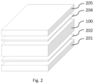
- FIG. 2 is a three-dimensional exploded structural diagram illustrating an electrochromic device helpful to understand the inventive concept.
- the electrochromic device of FIG. 2 may include the electrochromic device 100 of FIG. 1 , and may further include a bottom glass panel 201 and a top glass panel 205.
- the electrochromic device 100 of FIG. 1 may be sandwiched by the bottom glass panel 201 and the top glass panel 205. That is, the bottom electrode layer, the electrochromic layer, the electrolyte layer, the charge storage layer, and the top electrode layer may be sandwiched by the bottom glass panel 201 and the top glass panel 205.
- the bottom glass panel 201 and the top glass panel 205 may be adhered to the electrochromic device 100 of FIG. 1 through adhesive layers 202/204.
- the adhesive layers 202/204 may be any optically clear adhesive (OCA), PVB, EVA, SentryGlas, etc.
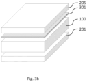
- FIGS. 3a and 3b are three-dimensional exploded structural diagrams illustrating electrochromic devices helpful to understand the inventive concept.
- the electrochromic device may include the electrochromic device of FIG. 2 (the adhesive layers 202/204 are omitted in FIGS. 3a and 3b ), and additionally include a reflective layer 301.
- the reflective layer 301 may be located either on a upper side of the top glass 205 panel contacting the top glass panel 205 (as shown in FIG. 3a ), or on a bottom side of the top glass panel 205 contacting the top glass panel 205 (as shown in FIG. 3b ).
- the reflective layer 301 may also be located on a side (either an upper side or a bottom side) of the bottom glass panel 201 contacting the bottom glass panel 201. Specific locations of the reflective layer 301 may be determined based on actual requirements and are not limited herein.
- the reflective layer 301 may be made of one or more metallic materials including, but not limited to, silver (Ag), aluminum (Al), chromium (Cr), gold (Au), other suitable metallic material, or any combination thereof.
- the reflective layer 301 may be a Bragg mirror comprising a plurality of dielectric layers.
- a dedicated reflective layer 301 is provided to reflect light.
- the reflective layer 301 may be removed and one of the bottom electrode layer and the top electrode layer may work as the reflective layer to reflect light.
- FIGS. 4a and 4b are schematic diagrams of electrochromic devices helpful to understand the inventive concept.
- the electrochromic device 410 may include a bottom electrode layer 101, an electrochromic layer 102 on the bottom electrode layer 101, a solid electrolyte layer 103 on the electrochromic layer 102, a charge storage layer 104 on the electrolyte layer 103, and a top electrode layer 105.
- the characteristics and the relative positional relationship of these component layers may be the same as those disclosed in the aforementioned implementations and thus will not be repeated herein.
- the bottom electrode layer 101 may be a reflective conductive layer that reflects incoming light
- the top electrode layer 105 may be a transparent conductive layer that allows incoming light to pass through.
- incoming light (indicated by a solid arrow line in FIG. 4a ) to the electrochromic device 410 may go through the top electrode layer 105 and be reflected by the bottom electrode layer 101 (a reflected light is indicated by a dash arrow line in FIG. 4a ).
- the solid state electrochromic device 410 may further include a bottom glass panel 401 beneath the bottom electrode layer 101, and a top glass panel 405 on the top electrode layer 105.
- the bottom and the top glass panels may provide support to the electrochromic device 410 to meet rigidness and toughness requirements of different applications.
- the bottom electrode layer 101 is a reflective layer and the top electrode layer 105 is a transparent layer.
- This inventive concept is not limited herein.
- the bottom electrode layer 101 may be a transparent conductive layer and the top electrode layer 105 may be a reflective conductive layer, as shown in FIG. 4b .
- the electrochromic device 420 of FIG. 4b may have the same structure as the electrochromic device 410 of FIG. 4a , except that the top electrode layer 105 is a reflective conductive layer, and the bottom electrode layer 101 is a transparent conductive layer.
- incoming light indicated by a solid arrow light in FIG.
- the electrochromic device 410 may go through the bottom electrode layer 101 and be reflected by the top electrode layer 105 (a reflected light is indicated by a dash arrow line in FIG. 4b ).
- the electrochromic device may comprise two states, a bright state and a dimming state, which may have different reflectivity properties.
- one of the electrode layers of the electrochromic device may work as a reflect layer to reflect incoming light.
- a separated reflective film may be omitted, which simplifies the structure of the electrochromic device and the manufacturing process thereof.
- FIG. 5 is a flowchart illustrating an electrochromic device manufacturing method helpful to understand the inventive concept but not falling under the claims. Referring to FIG. 5 , the manufacturing method may include the following steps S510 through S570.
- a bottom substrate may be provided, and an electrochromic layer may be formed on the bottom substrate.
- a top substrate may be provided, and a charge storage layer may be formed on the top substrate.
- the bottom substrate and the top substrate may be rigid substrates and may be made of materials including, but not limited to, glass/ITO.
- the bottom substrate and the top substrate may be flexible substrates and may be made of materials including, but not limited to, PET/ITO.
- the bottom substrate and the top substrate may be made of conductive materials and may work as a bottom electrode layer and a top electrode layer of the electrochromic device, respectively, and may each have a sheet resistance in a range of 0.01 S2/sq to 200 ⁇ /sq.
- a reflective layer may be formed on a side of one of the bottom substrate and the top substrate.
- the reflective layer may be made of one or more metallic materials including, but not limited to, silver (Ag), aluminum (Al), chromium (Cr), gold (Au), other suitable metallic material, or any combination thereof, which is not limited in this inventive concept.
- the electrochromic layer, the charge storage layer, and the electrolyte layer may be formed by deposition, coating, or any other suitable methods that are known to persons or ordinary skills in the art.
- the electrochromic layer and the electrolyte layer may be sequentially deposited on the bottom substrate using a wet process, such as spin-coating, ink-jetting, slot-die coating, dip-coating, gravure-coating, spray-coating, blade-coating, screen printing, mayer bar coating, relief printing, etc.
- the charge storage layer may be deposited on the top substrate using a wet process, such as spin-coating, ink-jetting, slot-die coating, dip-coating, gravure-coating, spray-coating, blade-coating, screen printing, mayer bar coating, relief printing, etc.
- a wet process such as spin-coating, ink-jetting, slot-die coating, dip-coating, gravure-coating, spray-coating, blade-coating, screen printing, mayer bar coating, relief printing, etc.
- step S550 the electrolyte layer on the electrochromic layer may be laminated with the charge storage layer (along with the top substrate). After step S550, the electrochromic layer, the electrolyte layer, and the charge storage layer are sandwiched by the bottom substrate and the top substrate.
- the electrolyte layer may be cured.
- the electrolyte layer may be cured by UV exposure, heat, pressure, or other suitable methods, and this inventive concept is not limited in this regard.
- the electrochromic layer, the electrolyte layer, and the charge storage layer may form the electrochromic device.
- a transmittance of the electrochromic device may range from 0.1% to 99%.
- the electrolyte layer may be deposited on the electrochromic layer, and then maybe laminated by the charge storage layer (along with the top substrate).
- This inventive concept is not limited herein.
- the electrolyte layer may be deposited on the charge storage layer on the top substrate, and then be laminated by the electrochromic layer (along with the bottom substrate).
- a top glass panel and a bottom glass panel may further be provided.
- the top and the bottom glass panels may sandwich the electrochromic device to provide support to meet rigidness and toughness requirements of different applications. Specific characteristics of component layers may be the same as those described in the aforementioned implementations, and thus will not be repeated herein.
- the electrochromic device may be switched between two states, a bright state and a dimming state, which have different reflectivity properties as further described in FIG. 8 .
- the reflective layer may be located on a side of the top glass panel or a side of bottom glass panel.
- the electrochromic layer may not necessarily include a separated reflective layer.
- one of the bottom substrate and the top substrate may be a reflective layer while the other of the bottom substrate and the top substrate being a transparent layer. Relevant parts of above descriptions may be referred to for details, which is not repeatedly described herein.
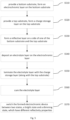
- FIG. 6 is a flowchart illustrating an electrochromic device manufacturing method in accordance with one embodiment of the inventive concept as claimed.
- the electrochromic device manufacturing method may include the following steps S610 through S670.
- Step S610 and step S620 may be the same with step S510 and step S520, respectively, of the aforementioned method described by reference to Fig.S. Relevant parts of the above description may be referred to for details of these steps, which are not repeatedly described herein.
- step S630 the bottom substrate (along with the electrochromic layer formed on it) is fixed to the top substrate (along with the charge storage layer formed on it), so that a space is formed between the electrochromic layer and the charge storage layer.
- the bottom substrate may be fixed to the top substrate by, for example, gluing the bottom substrate to the top substrate. Other methods that can fix the bottom substrate to the top substrate are contemplated, and this inventive concept is not limited herein.
- a distance d between the electrochromic layer and the charge storage layer may be predetermined. In embodiments pursuant to the claimed invention, one or more spacers is provided to maintain the distance between the electrochromic layer and the charge storage layer. A specific value of the distance may be chosen according to actual requirements, for example, of a specific application, and is not limited herein.
- An opening is formed at the edge for a subsequent filling-in process.
- step S650 the opening is sealed after the filling-in process.
- the electrolyte liquid in the space may be cured to form an electrolyte layer.
- the electrolyte liquid in the space may be cured by UV exposure, heat, pressure, or other suitable methods, and this inventive concept is not limited in this regard.
- step S670 the electrochromic device may be switched between two states, a bright state and a dimming state, which may have different reflectivity properties, as will be further described in FIG. 8 .
- FIG. 7 is a diagram illustrating a vacuum-suction process in accordance with one embodiment of the claimed inventive concept.
- the vacuum-suction process is implemented in step 640 of FIG. 6 .
- the vacuum-suction process includes the following steps. First, after the space 710 is created between the electrochromic layer 702 and the charge storage layer 704, edge seals 707 are added at edge areas of the electrochromic layer 702 and the charge storage layer 704 to seal the space 710. In embodiments pursuant to the claimed invention, one or more spacers 708 are provided to maintain a distance between the electrochromic layer 702 and the charge storage layer 704. Second, the space 710 is vacuumed.
- Vacuuming methods that are well known to persons of ordinary skills in the arts may be used to vacuum the space 710, which is not limited herein.
- electrochromic solution 720 is sucked trough the opening formed in step S630 into the vacuumed space 710 to fill the space 710, so that an electrolyte layer between the electrochromic layer 702 and the charge storage layer 704 is formed.
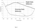
- Fig. 8 is a diagram illustrating two distinct modes or states in accordance with the electrochromic device described with respect to FIGS. 1 , 2 , 3a , 3b , 4a , and 4b
- the two distinct modes or states of the electrochromic device may comprise a bright state and a dimming state between which the electrochromic device may switch.
- the bright state and the dimming state have different reflective properties at specific wavelengths.
- the electrochromic device in the bright state may have a higher transparency for wavelengths between about 380nm and 780 nm compared to the electrochromic device in the dimming state.
- the manufacturing method may further include forming a top glass panel and a bottom glass panel that sandwich the electrochromic device. This step may be the same as that described in aforementioned embodiments. Relevant parts in those embodiments may be referred to for details, which will not be repeated herein.
- the manufacturing method may further include forming a reflective layer.
- the reflective layer may be located on a side of the top glass panel or a side of bottom glass panel.
- the electrochromic layer may not necessarily include a separate reflective layer.
- one of the bottom substrate and the top substrate may be a reflective layer while the other of the bottom substrate and the top substrate may be a transparent layer. Relevant parts of above descriptions may be referred to for details, which will not be repeated herein.
- one of the top electrode layer and the bottom electrode layer may be a reflective layer for reflecting light, while the other may be a transparent layer.
- These devices have a simplified structure due to the removal of a separate reflective layer. Since the process of pasting a reflective film in the electrochromic device is no longer necessary, the manufacturing process may be simplified. Additionally, in a disclosed manufacturing method, a vacuum-suction process is used to form the electrolyte layer, which may further improve the efficiency of the manufacturing process.
Landscapes
- Physics & Mathematics (AREA)
- Nonlinear Science (AREA)
- General Physics & Mathematics (AREA)
- Optics & Photonics (AREA)
- Chemical & Material Sciences (AREA)
- Chemical Kinetics & Catalysis (AREA)
- Electrochemistry (AREA)
- Inorganic Chemistry (AREA)
- Electrochromic Elements, Electrophoresis, Or Variable Reflection Or Absorption Elements (AREA)
Description
- This application relates generally to technical field of electronics, and more specifically, to electrochromic devices with reflective structures.
- Electrochromic materials can change their optical characteristics, such as transmittance, reflectance, absorptance or emittance under electrical current or voltage, and thus have numerous applications in scenarios that require devices that have adjustable optical properties (e.g., dimmable devices). For example, dimmable mirrors and dimmable windows that are made of electrochromic materials have been ubiquitously used in various places, including vehicles, airplanes, and buildings, to provide better adaption for different lighting conditions.
- The manufacturing of dimmable devices with electrochromic materials, however, remains a challenging task due to complicated processes to deal with various component layers and issues related to sealing and diffusion of electrochromic materials during the manufacturing process. Therefore, an efficient and reliable manufacturing process is desirable.
US2003/137712 discloses an electrochromic device with variable reflective and transmission properties.
US2007/097483 discloses an electrochromic device with a reflection layer on top of the substrate.KR20170125573
KR20190071996
JP2011164256 JPH11282023A - In a first aspect of the present invention, there is provided an electrochromic device manufacturing method according to
claim 1. - The electrochromic device manufacturing method includes: providing a top electrode layer, forming a charge storage layer on the top electrode layer, providing a bottom electrode layer, forming an electrochromic layer on the bottom electrode layer, and forming an electrolyte layer sandwiched by the charge storage layer and the electrochromic layer, comprising steps of: fixing the top electrode layer to the bottom electrode layer, the charge storage layer and the electrochromic layer located between the top electrode layer and the bottom electrode layer and separated by a space; providing edge seals at edges areas of the electrochromic layer and the charge storage layer to seal the space; providing one or more spacers within the space to maintain a predetermined distance between the electrochromic layer and the charge storage layer; and thereafter, vacuuming the space and filling it with an electrolyte liquid by vacuum suction through an opening formed in the edge seal, which opening is sealed after the filling process is completed. The electrochromic layer, the electrolyte layer, and the charge storage layer are sandwiched by the top electrode layer and the bottom electrode layer. A transmittance of the electrochromic device changes in response to a voltage applied between the bottom electrode layer and the top electrode layer.
- In some examples, in the aforementioned method, the bottom electrode layer and the top electrode layer may each have a sheet resistance in a range of 0.01Ω/sq to 200Ω/sq.
- In some examples, the aforementioned method may further include: forming a top glass panel, a bottom glass panel and a reflective layer. The bottom electrode layer, the electrochromic layer, the electrolyte layer, the charge storage layer, and the top electrode layer may be sandwiched by the top glass panel and the bottom glass panel. The reflecting layer may be located on a side of the top glass panel contacting the top glass panel, or on a side of the bottom glass panel contacting the bottom glass panel.
- In some examples, in the aforementioned method, the reflective layer may be a metallic layer made of Ag, Al, Cr, or Au.
- In some examples, in the aforementioned method, the reflective layer may be a Bragg mirror comprising a plurality of dielectric layers.
- In some examples, in the aforementioned method, one of the bottom electrode layer and the top electrode layer may be a reflective conductive layer, and the other of the bottom electrode layer and the top electrode layer may be a transparent conductive layer.
- In some examples, the aforementioned method may further include: forming a top glass panel and a bottom glass panel. The bottom electrode layer, the electrochromic layer, the electrolyte layer, the charge storage layer, and the top electrode layer may be sandwiched by the top glass panel and the bottom glass panel.
- In some exemplary electrochromic devices, one of the top electrode layer and the bottom electrode layer may be a reflective layer for reflecting light, while the other may be a transparent layer. These devices have a simplified structure due to the removal of a dedicated reflective layer, which may also result in simplified manufacturing process since the process of pasting a reflective film in the electrochromic device is no longer necessary.
- Preferred and non-limiting embodiments of this inventive concept may be more readily understood by referring to the accompanying drawings. The accompanying drawings, which are incorporated in and constitute a part of the description, illustrate embodiments in accordance with this inventive concept and, together with the description, serve to explain the disclosed inventive concept. It is apparent that these drawings present only some embodiments of the inventive concept and persons of ordinary skill in the art may obtain drawings of other embodiments from them without creative effort.
-
FIG. 1 . is a schematic diagram of an electrochromic device helpful to understand the inventive concept of the claimed electrochromic device manufacturing method. -
FIG. 2 . is a three-dimensional exploded structural diagram illustrating an electrochromic device helpful to understand the inventive concept of the claimed electrochromic device manufacturing method. -
FIGS. 3a and3b are three-dimensional exploded structural diagrams illustrating electrochromic devices helpful to understand the inventive concept of the claimed electrochromic device manufacturing method. -
FIGS. 4a and4b are schematic diagrams of electrochromic devices helpful to understand the inventive concept of the claimed electrochromic device manufacturing method. -
FIG. 5 is a flowchart illustrating an electrochromic device manufacturing method which is however not covered by the claims. -
FIG. 6 is a flowchart illustrating an electrochromic device manufacturing method in accordance with one embodiment of the inventive concept as claimed. -
FIG. 7 is a diagram illustrating a vacuum-suction filling process in accordance with one embodiment of the inventive concept as claimed. -
FIG. 8 is a diagram illustrating two distinct modes or states in accordance with the electrochromic devices described with respect toFIGS. 1 ,2 ,3a ,3b ,4a , and4b . -
FIG. 1 . is a schematic diagram of an electrochromic device helpful to understand the inventive concept. Referring toFIG. 1 , theelectrochromic device 100 may include anelectrochromic layer 102, anelectrolyte layer 103 on theelectrochromic layer 102, and acharge storage layer 104 on theelectrolyte layer 103. In some implementations, theelectrochromic device 100 may further include afirst substrate 101 beneath theelectrochromic layer 102, and asecond substrate 105 on thecharge storage layer 104. That is, theelectrochromic layer 102, thesolid electrolyte layer 103, and thecharge storage layer 104 may be sandwiched by thefirst substrate 101 and thesecond substrate 105. - The
first substrate 101 and thesecond substrate 105 may be made of conductive materials and may work as a bottom electrode layer and a top electrode layer of theelectrochromic device 100, respectively. Thus, thefirst substrate 101 may be termed thebottom electrode layer 101, and thesecond substrate 105 may be termed thetop electrode layer 105 in the rest of the application. A voltage may be applied between thebottom electrode layer 101 and thetop electrode layer 105, and a transmittance of the electrochromic device may change in response to the voltage applied between thebottom electrode layer 101 and thetop electrode layer 105. - In some implementations, , the
bottom electrode layer 101 and thetop electrode layer 105 may each comprise polyethylene terephthalate (PET) and indium tin oxide (ITO), and may each have a sheet resistance in a range of 0.01Ω/sq to 200Ω/sq. - In some implementations, , depending on the voltage applied between the
bottom electrode layer 101 and thetop electrode layer 105, the transmittance of the electrochromic film may range from 0.01% to 99%. - In some implementations, one of the
bottom electrode layer 101 and thetop electrode layer 105 may be a reflective conductive layer, and the other of thebottom electrode layer 101 and thetop electrode layer 105 may be a transparent conductive layer. - The
electrochromic device 100 may comprise two states, a bright state and a dimming state, which may have different reflectivity properties. -
FIG. 2 . is a three-dimensional exploded structural diagram illustrating an electrochromic device helpful to understand the inventive concept. Referring toFIG. 2 , the electrochromic device ofFIG. 2 may include theelectrochromic device 100 ofFIG. 1 , and may further include abottom glass panel 201 and atop glass panel 205. Theelectrochromic device 100 ofFIG. 1 may be sandwiched by thebottom glass panel 201 and thetop glass panel 205. That is, the bottom electrode layer, the electrochromic layer, the electrolyte layer, the charge storage layer, and the top electrode layer may be sandwiched by thebottom glass panel 201 and thetop glass panel 205. Thebottom glass panel 201 and thetop glass panel 205 may be adhered to theelectrochromic device 100 ofFIG. 1 throughadhesive layers 202/204. In one example, theadhesive layers 202/204 may be any optically clear adhesive (OCA), PVB, EVA, SentryGlas, etc. -
FIGS. 3a and3b are three-dimensional exploded structural diagrams illustrating electrochromic devices helpful to understand the inventive concept. Referring toFIGS. 3a and3b , the electrochromic device may include the electrochromic device ofFIG. 2 (theadhesive layers 202/204 are omitted inFIGS. 3a and3b ), and additionally include areflective layer 301. Thereflective layer 301 may be located either on a upper side of thetop glass 205 panel contacting the top glass panel 205 (as shown inFIG. 3a ), or on a bottom side of thetop glass panel 205 contacting the top glass panel 205 (as shown inFIG. 3b ). Alternatively, thereflective layer 301 may also be located on a side (either an upper side or a bottom side) of thebottom glass panel 201 contacting thebottom glass panel 201. Specific locations of thereflective layer 301 may be determined based on actual requirements and are not limited herein. - In some implementations, the
reflective layer 301 may be made of one or more metallic materials including, but not limited to, silver (Ag), aluminum (Al), chromium (Cr), gold (Au), other suitable metallic material, or any combination thereof. In some implementations, thereflective layer 301 may be a Bragg mirror comprising a plurality of dielectric layers. When an electrochromic device includes a dedicated reflective layer as shown, for example, inFIGS. 3a and3b , both the bottom electrode layer and the top electrode layer will be a transparent conductive layer. - In the implementations shown in
FIGS. 3a and3b , a dedicatedreflective layer 301 is provided to reflect light. In some embodiments, thereflective layer 301 may be removed and one of the bottom electrode layer and the top electrode layer may work as the reflective layer to reflect light. These implementations will be described below with reference toFIGS. 4a and4b . -
FIGS. 4a and4b are schematic diagrams of electrochromic devices helpful to understand the inventive concept. As shown inFIG. 4a , theelectrochromic device 410 may include abottom electrode layer 101, anelectrochromic layer 102 on thebottom electrode layer 101, asolid electrolyte layer 103 on theelectrochromic layer 102, acharge storage layer 104 on theelectrolyte layer 103, and atop electrode layer 105. The characteristics and the relative positional relationship of these component layers may be the same as those disclosed in the aforementioned implementations and thus will not be repeated herein. - As shown in
FIG. 4a , in theelectrochromic device 410, thebottom electrode layer 101 may be a reflective conductive layer that reflects incoming light, and thetop electrode layer 105 may be a transparent conductive layer that allows incoming light to pass through. Thus incoming light (indicated by a solid arrow line inFIG. 4a ) to theelectrochromic device 410 may go through thetop electrode layer 105 and be reflected by the bottom electrode layer 101 (a reflected light is indicated by a dash arrow line inFIG. 4a ). - In some implementations, the solid state
electrochromic device 410 may further include abottom glass panel 401 beneath thebottom electrode layer 101, and atop glass panel 405 on thetop electrode layer 105. The bottom and the top glass panels may provide support to theelectrochromic device 410 to meet rigidness and toughness requirements of different applications. - In the electrochromic device shown in
FIG. 4a , thebottom electrode layer 101 is a reflective layer and thetop electrode layer 105 is a transparent layer. This inventive concept, however, is not limited herein. In some implementations, thebottom electrode layer 101 may be a transparent conductive layer and thetop electrode layer 105 may be a reflective conductive layer, as shown inFIG. 4b . Theelectrochromic device 420 ofFIG. 4b may have the same structure as theelectrochromic device 410 ofFIG. 4a , except that thetop electrode layer 105 is a reflective conductive layer, and thebottom electrode layer 101 is a transparent conductive layer. Thus, as shown inFIG. 4b , incoming light (indicated by a solid arrow light inFIG. 4b ) to theelectrochromic device 410 may go through thebottom electrode layer 101 and be reflected by the top electrode layer 105 (a reflected light is indicated by a dash arrow line inFIG. 4b ). The electrochromic device may comprise two states, a bright state and a dimming state, which may have different reflectivity properties. - In the implementations of
FIGS. 4a and4b , rather than providing a separated reflective layer to reflect light, one of the electrode layers of the electrochromic device may work as a reflect layer to reflect incoming light. Thus, a separated reflective film may be omitted, which simplifies the structure of the electrochromic device and the manufacturing process thereof. - The claimed inventive concept provides an electrochromic device manufacturing methods.
FIG. 5 is a flowchart illustrating an electrochromic device manufacturing method helpful to understand the inventive concept but not falling under the claims. Referring toFIG. 5 , the manufacturing method may include the following steps S510 through S570. - In step S510, a bottom substrate may be provided, and an electrochromic layer may be formed on the bottom substrate.
- In step S520, a top substrate may be provided, and a charge storage layer may be formed on the top substrate.
- In some implementations, , the bottom substrate and the top substrate may be rigid substrates and may be made of materials including, but not limited to, glass/ITO. In some implementations, the bottom substrate and the top substrate may be flexible substrates and may be made of materials including, but not limited to, PET/ITO. The bottom substrate and the top substrate may be made of conductive materials and may work as a bottom electrode layer and a top electrode layer of the electrochromic device, respectively, and may each have a sheet resistance in a range of 0.01 S2/sq to 200Ω/sq.
- In step S530, a reflective layer may be formed on a side of one of the bottom substrate and the top substrate. The reflective layer may be made of one or more metallic materials including, but not limited to, silver (Ag), aluminum (Al), chromium (Cr), gold (Au), other suitable metallic material, or any combination thereof, which is not limited in this inventive concept.
- In step S540, an electrolyte layer may be deposited on the electrochromic layer on the electrochromic layer the bottom substrate.
- In steps S510 through S540, the electrochromic layer, the charge storage layer, and the electrolyte layer may be formed by deposition, coating, or any other suitable methods that are known to persons or ordinary skills in the art. For example, the electrochromic layer and the electrolyte layer may be sequentially deposited on the bottom substrate using a wet process, such as spin-coating, ink-jetting, slot-die coating, dip-coating, gravure-coating, spray-coating, blade-coating, screen printing, mayer bar coating, relief printing, etc. The charge storage layer may be deposited on the top substrate using a wet process, such as spin-coating, ink-jetting, slot-die coating, dip-coating, gravure-coating, spray-coating, blade-coating, screen printing, mayer bar coating, relief printing, etc. Specific methods that may be used to form the electrochromic layer, the charge storage layer, and the electrolyte layer are not limited in this inventive concept.
- In step S550, the electrolyte layer on the electrochromic layer may be laminated with the charge storage layer (along with the top substrate). After step S550, the electrochromic layer, the electrolyte layer, and the charge storage layer are sandwiched by the bottom substrate and the top substrate.
- In step S560, the electrolyte layer may be cured. The electrolyte layer may be cured by UV exposure, heat, pressure, or other suitable methods, and this inventive concept is not limited in this regard. The electrochromic layer, the electrolyte layer, and the charge storage layer may form the electrochromic device. Depending on a voltage applied between the bottom substrate and the top substrate, a transmittance of the electrochromic device may range from 0.1% to 99%.
- In the aforementioned implementation, after the electrochromic layer has been formed on the bottom substrate and the charge storage layer has been formed on the top substrate, the electrolyte layer may be deposited on the electrochromic layer, and then maybe laminated by the charge storage layer (along with the top substrate). This inventive concept is not limited herein. In one example, the electrolyte layer may be deposited on the charge storage layer on the top substrate, and then be laminated by the electrochromic layer (along with the bottom substrate).
- After
Step 560, a top glass panel and a bottom glass panel may further be provided. The top and the bottom glass panels may sandwich the electrochromic device to provide support to meet rigidness and toughness requirements of different applications. Specific characteristics of component layers may be the same as those described in the aforementioned implementations, and thus will not be repeated herein. Instep 570, the electrochromic device may be switched between two states, a bright state and a dimming state, which have different reflectivity properties as further described inFIG. 8 . - In some implementations, the reflective layer may be located on a side of the top glass panel or a side of bottom glass panel. Alternatively, the electrochromic layer may not necessarily include a separated reflective layer. Instead, one of the bottom substrate and the top substrate may be a reflective layer while the other of the bottom substrate and the top substrate being a transparent layer. Relevant parts of above descriptions may be referred to for details, which is not repeatedly described herein.
-
FIG. 6 is a flowchart illustrating an electrochromic device manufacturing method in accordance with one embodiment of the inventive concept as claimed. Referring toFIG. 6 , the electrochromic device manufacturing method may include the following steps S610 through S670. - Step S610 and step S620 may be the same with step S510 and step S520, respectively, of the aforementioned method described by reference to Fig.S. Relevant parts of the above description may be referred to for details of these steps, which are not repeatedly described herein.
- In step S630, the bottom substrate (along with the electrochromic layer formed on it) is fixed to the top substrate (along with the charge storage layer formed on it), so that a space is formed between the electrochromic layer and the charge storage layer. The bottom substrate may be fixed to the top substrate by, for example, gluing the bottom substrate to the top substrate. Other methods that can fix the bottom substrate to the top substrate are contemplated, and this inventive concept is not limited herein. A distance d between the electrochromic layer and the charge storage layer may be predetermined. In embodiments pursuant to the claimed invention, one or more spacers is provided to maintain the distance between the electrochromic layer and the charge storage layer. A specific value of the distance may be chosen according to actual requirements, for example, of a specific application, and is not limited herein. An opening is formed at the edge for a subsequent filling-in process.
- In step S640, the space between the electrochromic layer and the charge storage layer is filled with electrolyte liquid by a vacuum-suction process which is described in
FIG. 7 . - In step S650, the opening is sealed after the filling-in process.
- In step S660, the electrolyte liquid in the space may be cured to form an electrolyte layer. The electrolyte liquid in the space may be cured by UV exposure, heat, pressure, or other suitable methods, and this inventive concept is not limited in this regard.
- In step S670, the electrochromic device may be switched between two states, a bright state and a dimming state, which may have different reflectivity properties, as will be further described in
FIG. 8 . -
FIG. 7 is a diagram illustrating a vacuum-suction process in accordance with one embodiment of the claimed inventive concept. The vacuum-suction process is implemented instep 640 ofFIG. 6 . Referring toFIG. 7 , the vacuum-suction process includes the following steps. First, after thespace 710 is created between theelectrochromic layer 702 and thecharge storage layer 704, edge seals 707 are added at edge areas of theelectrochromic layer 702 and thecharge storage layer 704 to seal thespace 710. In embodiments pursuant to the claimed invention, one ormore spacers 708 are provided to maintain a distance between theelectrochromic layer 702 and thecharge storage layer 704. Second, thespace 710 is vacuumed. Vacuuming methods that are well known to persons of ordinary skills in the arts may be used to vacuum thespace 710, which is not limited herein. Third,electrochromic solution 720 is sucked trough the opening formed in step S630 into the vacuumedspace 710 to fill thespace 710, so that an electrolyte layer between theelectrochromic layer 702 and thecharge storage layer 704 is formed. -
Fig. 8 is a diagram illustrating two distinct modes or states in accordance with the electrochromic device described with respect toFIGS. 1 ,2 ,3a ,3b ,4a , and4b InFIG. 8 , the two distinct modes or states of the electrochromic device may comprise a bright state and a dimming state between which the electrochromic device may switch. The bright state and the dimming state have different reflective properties at specific wavelengths. In some examples, the electrochromic device in the bright state may have a higher transparency for wavelengths between about 380nm and 780 nm compared to the electrochromic device in the dimming state. - In some embodiments, the manufacturing method may further include forming a top glass panel and a bottom glass panel that sandwich the electrochromic device. This step may be the same as that described in aforementioned embodiments. Relevant parts in those embodiments may be referred to for details, which will not be repeated herein.
- In some embodiments, the manufacturing method may further include forming a reflective layer. The reflective layer may be located on a side of the top glass panel or a side of bottom glass panel. Alternatively, the electrochromic layer may not necessarily include a separate reflective layer. In that case, one of the bottom substrate and the top substrate may be a reflective layer while the other of the bottom substrate and the top substrate may be a transparent layer. Relevant parts of above descriptions may be referred to for details, which will not be repeated herein.
- In the manufacturing methods herein disclosed, one of the top electrode layer and the bottom electrode layer may be a reflective layer for reflecting light, while the other may be a transparent layer. These devices have a simplified structure due to the removal of a separate reflective layer. Since the process of pasting a reflective film in the electrochromic device is no longer necessary, the manufacturing process may be simplified. Additionally, in a disclosed manufacturing method, a vacuum-suction process is used to form the electrolyte layer, which may further improve the efficiency of the manufacturing process.
- While examples and features of disclosed principles are described herein, modifications, adaptations, and other implementations are possible. Also, the words "comprising," "having," "containing," and "including," and other similar forms are intended to be equivalent in meaning and be open ended in that an item or items following any one of these words is not meant to be an exhaustive listing of such item or items, or meant to be limited to only the listed item or items. It must also be noted that as used herein and in the appended claims, the singular forms "a," "an," and "the" include plural references unless the context clearly dictates otherwise.
- The embodiments illustrated herein are described in sufficient detail to enable those skilled in the art to practice the teachings disclosed. Other embodiments may be used and derived therefrom, such that structural and logical substitutions and changes may be made without departing from the scope of the appended claims. The detailed description, therefore, is not to be taken in a limiting sense, and the scope of various embodiments is defined by the appended claims.
Claims (8)
- An electrochromic device manufacturing method, comprising:providing (S620) a top electrode layer (105);forming a charge storage layer (104; 704) on the top electrode layer;providing (S610) a bottom electrode layer (101);forming an electrochromic layer (102; 702) on the bottom electrode layer; andforming an electrolyte layer (103) sandwiched by the charge storage layer and the electrochromic layer, comprising the steps of:fixing (S630) the top electrode layer to the bottom electrode layer, the charge storage layer and the electrochromic layer located between the top electrode layer and the bottom electrode layer and separated by a space (710);providing edge seals at edge areas of the electrochromic layer and the charge storage layer to seal the space;providing one or more spacers (708) within the space to maintain a predetermined distance between the electrochromic layer and the charge storage layer; andthereafter, vacuuming the space and filling (S640) the vacuumed space with an electrolyte liquid by vacuum suction through an opening formed in the edge seal (707); sealing (S650) the opening after the filling process;wherein the electrochromic layer, the electrolyte layer, and the charge storage layer are sandwiched by the top electrode layer and the bottom electrode layer, and wherein the electrochromic device obtained by said manufacturing method is configured to change its transmittance in response to a voltage applied between the bottom electrode layer and the top electrode layer.
- The method of claim 1, wherein the bottom electrode layer and the top electrode layer each have a sheet resistance in a range of 0.01Ω/sq to 200Ω/sq.
- The method of claim 1, wherein the step of forming a charge storage layer on the top electrode layer comprises:depositing the charge storage layer on the top electrode layer using a wet process,and wherein the forming an electrochromic layer on the bottom electrode layer comprises:
depositing the electrochromic layer on the bottom electrode layer using a wet process. - The method of claim 1, further comprising:forming a top glass panel (205; 405) and a bottom glass panel (201; 401), wherein the bottom electrode layer, the electrochromic layer, the electrolyte layer, the charge storage layer, and the top electrode layer are sandwiched by the top glass panel and the bottom glass panel; andforming a reflective layer (301) on a side of the top glass panel contacting the top glass panel, or on a side of the bottom glass panel contacting the bottom glass panel.
- The method of claim 1, wherein the reflective layer is a metallic layer made of Ag, Al, Cr, or Au, or a Bragg mirror comprising a plurality of dielectric layers.
- The method of claim 1, wherein one of the bottom electrode layer and the top electrode layer is a reflective conductive layer, and the other of the bottom electrode layer and the top electrode layer is a transparent conductive layer.
- The method of claim 6, further comprising:
forming a top glass panel (205; 405) and a bottom glass panel (201; 401), wherein the bottom electrode layer, the electrochromic layer, the electrolyte layer, the charge storage layer, and the top electrode layer are sandwiched by the top glass panel and the bottom glass panel. - The method of claim 1, further comprising:
curing (S660) the electrolyte liquid by UV exposure, heat or pressure.
Applications Claiming Priority (1)
| Application Number | Priority Date | Filing Date | Title |
|---|---|---|---|
| US16/666,686 US11300845B2 (en) | 2019-10-29 | 2019-10-29 | Applications of electrochromic devices with reflective structure |
Publications (2)
| Publication Number | Publication Date |
|---|---|
| EP3816720A1 EP3816720A1 (en) | 2021-05-05 |
| EP3816720B1 true EP3816720B1 (en) | 2024-07-17 |
Family
ID=72147921
Family Applications (1)
| Application Number | Title | Priority Date | Filing Date |
|---|---|---|---|
| EP20191620.2A Active EP3816720B1 (en) | 2019-10-29 | 2020-08-18 | Electrochromic device manufacturing method |
Country Status (4)
| Country | Link |
|---|---|
| US (3) | US11300845B2 (en) |
| EP (1) | EP3816720B1 (en) |
| CN (1) | CN112817188A (en) |
| ES (1) | ES2987158T3 (en) |
Families Citing this family (1)
| Publication number | Priority date | Publication date | Assignee | Title |
|---|---|---|---|---|
| CN115291450B (en) * | 2022-08-19 | 2024-06-21 | 中国科学院苏州纳米技术与纳米仿生研究所 | Method for printing electrolyte layer, electrochromic device and preparation method thereof |
Citations (1)
| Publication number | Priority date | Publication date | Assignee | Title |
|---|---|---|---|---|
| JPH11282023A (en) * | 1998-03-30 | 1999-10-15 | Nippon Mitsubishi Oil Corp | Method for manufacturing electrochromic device |
Family Cites Families (20)
| Publication number | Priority date | Publication date | Assignee | Title |
|---|---|---|---|---|
| US5138013A (en) * | 1990-12-17 | 1992-08-11 | Ford Motor Company | Epoxy curable ion-conducting electrolyte useful in electrochromic devices |
| US6366017B1 (en) * | 1999-07-14 | 2002-04-02 | Agilent Technologies, Inc/ | Organic light emitting diodes with distributed bragg reflector |
| US6515787B1 (en) | 2000-03-07 | 2003-02-04 | Eclipse Energy Systems, Inc. | Electrochromic layer |
| WO2006052067A1 (en) * | 2004-11-11 | 2006-05-18 | Lg Chem, Ltd. | Electrochromic mirror or window displaying information |
| KR100870613B1 (en) | 2005-11-02 | 2008-11-25 | 주식회사 엘지화학 | Electrode Structure of Electrochromic Device |
| CA2764751C (en) * | 2009-06-11 | 2018-01-09 | Switch Materials Inc. | Variable transmittance optical filter and uses thereof |
| JP2011164256A (en) | 2010-02-08 | 2011-08-25 | Konica Minolta Holdings Inc | Electrochemical display element |
| US20140340729A1 (en) * | 2011-09-16 | 2014-11-20 | National Institute Of Advanced Industrial Science And Technology | Reflective dimming electrochromic element with non-water based hydrogen ion conductive electrolyte layer inserted therein, and dimming element using the same |
| KR20140041117A (en) * | 2012-09-27 | 2014-04-04 | 엘지이노텍 주식회사 | Electrochromic mirror and manufacturing method thereof |
| KR102063776B1 (en) * | 2012-12-17 | 2020-01-09 | 엘지이노텍 주식회사 | Electrochromic display device and manufacturing method thereof |
| US10061177B2 (en) * | 2014-07-23 | 2018-08-28 | Kinestral Technologies, Inc. | Process for preparing multi-layer electrochromic stacks |
| JP6617293B2 (en) * | 2014-08-07 | 2019-12-11 | パナソニックIpマネジメント株式会社 | Display device |
| US20160147125A1 (en) * | 2014-11-24 | 2016-05-26 | Freescale Semiconductor, Inc. | Electronic devices wth transparent conducting electrodes, and methods of manufacture thereof |
| US20170097551A1 (en) * | 2015-10-02 | 2017-04-06 | Heliotrope Technologies, Inc. | Electrochromic device containing distributed bragg reflector configured to selectively reflect uv radiation |
| KR101801668B1 (en) | 2016-05-04 | 2017-11-28 | 립하이 주식회사 | Electrochromic apparatus |
| CN108474990B (en) * | 2016-03-07 | 2021-05-07 | 力海科技股份有限公司 | Electrochromic device |
| KR102118358B1 (en) * | 2017-09-18 | 2020-06-04 | 주식회사 엘지화학 | Method for preparing an electrochromic device |
| KR101979307B1 (en) * | 2017-09-27 | 2019-05-16 | 고려대학교 산학협력단 | Reflector electrode for micro light emitting devices, micro light emitting devices having reflector electrode and manufacturing method thereof |
| KR102022784B1 (en) | 2017-12-15 | 2019-09-18 | 한양대학교 에리카산학협력단 | Electrochromic device and fabricating method of the same, and electrolyte of the same |
| CN114895498B (en) * | 2018-09-13 | 2024-04-16 | 深圳市光羿科技有限公司 | Preparation method of solid-state electrochromic device, solid-state electrolyte and application thereof |
-
2019
- 2019-10-29 US US16/666,686 patent/US11300845B2/en active Active
-
2020
- 2020-08-18 EP EP20191620.2A patent/EP3816720B1/en active Active
- 2020-08-18 ES ES20191620T patent/ES2987158T3/en active Active
- 2020-09-21 CN CN202010997679.1A patent/CN112817188A/en active Pending
-
2022
- 2022-03-14 US US17/694,061 patent/US11914261B2/en active Active
-
2024
- 2024-01-05 US US18/405,306 patent/US12554171B2/en active Active
Patent Citations (1)
| Publication number | Priority date | Publication date | Assignee | Title |
|---|---|---|---|---|
| JPH11282023A (en) * | 1998-03-30 | 1999-10-15 | Nippon Mitsubishi Oil Corp | Method for manufacturing electrochromic device |
Also Published As
| Publication number | Publication date |
|---|---|
| ES2987158T3 (en) | 2024-11-13 |
| CN112817188A (en) | 2021-05-18 |
| US20240142842A1 (en) | 2024-05-02 |
| US12554171B2 (en) | 2026-02-17 |
| US20210124230A1 (en) | 2021-04-29 |
| US11300845B2 (en) | 2022-04-12 |
| US20220197099A1 (en) | 2022-06-23 |
| EP3816720A1 (en) | 2021-05-05 |
| US11914261B2 (en) | 2024-02-27 |
Similar Documents
| Publication | Publication Date | Title |
|---|---|---|
| EP2342411B1 (en) | Switchable glazings | |
| EP1952194B1 (en) | Electrochromic system on a plastic substrate | |
| US12088749B2 (en) | Display-module assembly and electronic device | |
| KR20150031917A (en) | Electrode Plate and Eletrochomic Plate, Electrochomic Mirror and Display Device Using the Same | |
| JP2016525951A (en) | Laminated glazing | |
| KR20090034948A (en) | Glazing type electrochemical and / or electrically controllable device with variable optical and / or energy properties | |
| JP7452051B2 (en) | Light control sheet, its manufacturing method, and laminated glass using the same | |
| CN114981078A (en) | Glazing with light source | |
| US20220105710A1 (en) | Light modulating device and manufacturing method therefor | |
| CN109601014A (en) | With the electric control gear for the scattering that liquid crystal is changed can be passed through | |
| KR20140041117A (en) | Electrochromic mirror and manufacturing method thereof | |
| CN110831765A (en) | Functional elements with electronically controllable optical properties | |
| US12554171B2 (en) | Applications of electrochromic devices with reflective structure | |
| US10095333B2 (en) | Touch apparatus | |
| JP2024015005A (en) | Light control device, laminate for light control device, and light control cell | |
| JP7172262B2 (en) | Light control film and its manufacturing method | |
| CN217543619U (en) | Light modulation device and light modulation device | |
| CN113711118A (en) | Dimming sheet and dimming device | |
| WO2026067599A1 (en) | Laminated assembly and preparation method therefor, and vehicle | |
| US9778795B2 (en) | Touch apparatus | |
| EP3898229A1 (en) | Glazing comprising a switchable device, laminated structure and method for manufacturing of a glazing | |
| US20240142846A1 (en) | Light path control device and manufacturing method thereof | |
| HK40045118A (en) | Applications of electrochromic devices with reflective structure | |
| CN120359121A (en) | Glazing panel | |
| CN114551756A (en) | Display device and method for manufacturing display device |
Legal Events
| Date | Code | Title | Description |
|---|---|---|---|
| PUAI | Public reference made under article 153(3) epc to a published international application that has entered the european phase |
Free format text: ORIGINAL CODE: 0009012 |
|
| STAA | Information on the status of an ep patent application or granted ep patent |
Free format text: STATUS: REQUEST FOR EXAMINATION WAS MADE |
|
| 17P | Request for examination filed |
Effective date: 20200818 |
|
| AK | Designated contracting states |
Kind code of ref document: A1 Designated state(s): AL AT BE BG CH CY CZ DE DK EE ES FI FR GB GR HR HU IE IS IT LI LT LU LV MC MK MT NL NO PL PT RO RS SE SI SK SM TR |
|
| STAA | Information on the status of an ep patent application or granted ep patent |
Free format text: STATUS: EXAMINATION IS IN PROGRESS |
|
| 17Q | First examination report despatched |
Effective date: 20221109 |
|
| P01 | Opt-out of the competence of the unified patent court (upc) registered |
Effective date: 20230511 |
|
| GRAP | Despatch of communication of intention to grant a patent |
Free format text: ORIGINAL CODE: EPIDOSNIGR1 |
|
| STAA | Information on the status of an ep patent application or granted ep patent |
Free format text: STATUS: GRANT OF PATENT IS INTENDED |
|
| RIC1 | Information provided on ipc code assigned before grant |
Ipc: G02F 1/161 20060101ALI20240124BHEP Ipc: G02F 1/157 20060101ALI20240124BHEP Ipc: G02F 1/155 20060101AFI20240124BHEP |
|
| INTG | Intention to grant announced |
Effective date: 20240212 |
|
| GRAS | Grant fee paid |
Free format text: ORIGINAL CODE: EPIDOSNIGR3 |
|
| GRAA | (expected) grant |
Free format text: ORIGINAL CODE: 0009210 |
|
| STAA | Information on the status of an ep patent application or granted ep patent |
Free format text: STATUS: THE PATENT HAS BEEN GRANTED |
|
| AK | Designated contracting states |
Kind code of ref document: B1 Designated state(s): AL AT BE BG CH CY CZ DE DK EE ES FI FR GB GR HR HU IE IS IT LI LT LU LV MC MK MT NL NO PL PT RO RS SE SI SK SM TR |
|
| REG | Reference to a national code |
Ref country code: CH Ref legal event code: EP |
|
| REG | Reference to a national code |
Ref country code: DE Ref legal event code: R096 Ref document number: 602020033996 Country of ref document: DE |
|
| REG | Reference to a national code |
Ref country code: IE Ref legal event code: FG4D |
|
| REG | Reference to a national code |
Ref country code: LT Ref legal event code: MG9D |
|
| REG | Reference to a national code |
Ref country code: ES Ref legal event code: FG2A Ref document number: 2987158 Country of ref document: ES Kind code of ref document: T3 Effective date: 20241113 |
|
| REG | Reference to a national code |
Ref country code: NL Ref legal event code: MP Effective date: 20240717 |
|
| PG25 | Lapsed in a contracting state [announced via postgrant information from national office to epo] |
Ref country code: PT Free format text: LAPSE BECAUSE OF FAILURE TO SUBMIT A TRANSLATION OF THE DESCRIPTION OR TO PAY THE FEE WITHIN THE PRESCRIBED TIME-LIMIT Effective date: 20241118 |
|
| REG | Reference to a national code |
Ref country code: AT Ref legal event code: MK05 Ref document number: 1704704 Country of ref document: AT Kind code of ref document: T Effective date: 20240717 |
|
| PG25 | Lapsed in a contracting state [announced via postgrant information from national office to epo] |
Ref country code: NL Free format text: LAPSE BECAUSE OF FAILURE TO SUBMIT A TRANSLATION OF THE DESCRIPTION OR TO PAY THE FEE WITHIN THE PRESCRIBED TIME-LIMIT Effective date: 20240717 |
|
| PG25 | Lapsed in a contracting state [announced via postgrant information from national office to epo] |
Ref country code: PT Free format text: LAPSE BECAUSE OF FAILURE TO SUBMIT A TRANSLATION OF THE DESCRIPTION OR TO PAY THE FEE WITHIN THE PRESCRIBED TIME-LIMIT Effective date: 20241118 Ref country code: NL Free format text: LAPSE BECAUSE OF FAILURE TO SUBMIT A TRANSLATION OF THE DESCRIPTION OR TO PAY THE FEE WITHIN THE PRESCRIBED TIME-LIMIT Effective date: 20240717 |
|
| PG25 | Lapsed in a contracting state [announced via postgrant information from national office to epo] |
Ref country code: NO Free format text: LAPSE BECAUSE OF FAILURE TO SUBMIT A TRANSLATION OF THE DESCRIPTION OR TO PAY THE FEE WITHIN THE PRESCRIBED TIME-LIMIT Effective date: 20241017 |
|
| PG25 | Lapsed in a contracting state [announced via postgrant information from national office to epo] |
Ref country code: GR Free format text: LAPSE BECAUSE OF FAILURE TO SUBMIT A TRANSLATION OF THE DESCRIPTION OR TO PAY THE FEE WITHIN THE PRESCRIBED TIME-LIMIT Effective date: 20241018 Ref country code: FI Free format text: LAPSE BECAUSE OF FAILURE TO SUBMIT A TRANSLATION OF THE DESCRIPTION OR TO PAY THE FEE WITHIN THE PRESCRIBED TIME-LIMIT Effective date: 20240717 Ref country code: PL Free format text: LAPSE BECAUSE OF FAILURE TO SUBMIT A TRANSLATION OF THE DESCRIPTION OR TO PAY THE FEE WITHIN THE PRESCRIBED TIME-LIMIT Effective date: 20240717 |
|
| PG25 | Lapsed in a contracting state [announced via postgrant information from national office to epo] |
Ref country code: BG Free format text: LAPSE BECAUSE OF FAILURE TO SUBMIT A TRANSLATION OF THE DESCRIPTION OR TO PAY THE FEE WITHIN THE PRESCRIBED TIME-LIMIT Effective date: 20240717 |
|
| PG25 | Lapsed in a contracting state [announced via postgrant information from national office to epo] |
Ref country code: LV Free format text: LAPSE BECAUSE OF FAILURE TO SUBMIT A TRANSLATION OF THE DESCRIPTION OR TO PAY THE FEE WITHIN THE PRESCRIBED TIME-LIMIT Effective date: 20240717 |
|
| PG25 | Lapsed in a contracting state [announced via postgrant information from national office to epo] |
Ref country code: IS Free format text: LAPSE BECAUSE OF FAILURE TO SUBMIT A TRANSLATION OF THE DESCRIPTION OR TO PAY THE FEE WITHIN THE PRESCRIBED TIME-LIMIT Effective date: 20241117 Ref country code: AT Free format text: LAPSE BECAUSE OF FAILURE TO SUBMIT A TRANSLATION OF THE DESCRIPTION OR TO PAY THE FEE WITHIN THE PRESCRIBED TIME-LIMIT Effective date: 20240717 |
|
| PG25 | Lapsed in a contracting state [announced via postgrant information from national office to epo] |
Ref country code: HR Free format text: LAPSE BECAUSE OF FAILURE TO SUBMIT A TRANSLATION OF THE DESCRIPTION OR TO PAY THE FEE WITHIN THE PRESCRIBED TIME-LIMIT Effective date: 20240717 |
|
| PG25 | Lapsed in a contracting state [announced via postgrant information from national office to epo] |
Ref country code: RS Free format text: LAPSE BECAUSE OF FAILURE TO SUBMIT A TRANSLATION OF THE DESCRIPTION OR TO PAY THE FEE WITHIN THE PRESCRIBED TIME-LIMIT Effective date: 20241017 |
|
| PG25 | Lapsed in a contracting state [announced via postgrant information from national office to epo] |
Ref country code: RS Free format text: LAPSE BECAUSE OF FAILURE TO SUBMIT A TRANSLATION OF THE DESCRIPTION OR TO PAY THE FEE WITHIN THE PRESCRIBED TIME-LIMIT Effective date: 20241017 Ref country code: PL Free format text: LAPSE BECAUSE OF FAILURE TO SUBMIT A TRANSLATION OF THE DESCRIPTION OR TO PAY THE FEE WITHIN THE PRESCRIBED TIME-LIMIT Effective date: 20240717 Ref country code: NO Free format text: LAPSE BECAUSE OF FAILURE TO SUBMIT A TRANSLATION OF THE DESCRIPTION OR TO PAY THE FEE WITHIN THE PRESCRIBED TIME-LIMIT Effective date: 20241017 Ref country code: LV Free format text: LAPSE BECAUSE OF FAILURE TO SUBMIT A TRANSLATION OF THE DESCRIPTION OR TO PAY THE FEE WITHIN THE PRESCRIBED TIME-LIMIT Effective date: 20240717 Ref country code: IS Free format text: LAPSE BECAUSE OF FAILURE TO SUBMIT A TRANSLATION OF THE DESCRIPTION OR TO PAY THE FEE WITHIN THE PRESCRIBED TIME-LIMIT Effective date: 20241117 Ref country code: HR Free format text: LAPSE BECAUSE OF FAILURE TO SUBMIT A TRANSLATION OF THE DESCRIPTION OR TO PAY THE FEE WITHIN THE PRESCRIBED TIME-LIMIT Effective date: 20240717 Ref country code: GR Free format text: LAPSE BECAUSE OF FAILURE TO SUBMIT A TRANSLATION OF THE DESCRIPTION OR TO PAY THE FEE WITHIN THE PRESCRIBED TIME-LIMIT Effective date: 20241018 Ref country code: FI Free format text: LAPSE BECAUSE OF FAILURE TO SUBMIT A TRANSLATION OF THE DESCRIPTION OR TO PAY THE FEE WITHIN THE PRESCRIBED TIME-LIMIT Effective date: 20240717 Ref country code: BG Free format text: LAPSE BECAUSE OF FAILURE TO SUBMIT A TRANSLATION OF THE DESCRIPTION OR TO PAY THE FEE WITHIN THE PRESCRIBED TIME-LIMIT Effective date: 20240717 Ref country code: AT Free format text: LAPSE BECAUSE OF FAILURE TO SUBMIT A TRANSLATION OF THE DESCRIPTION OR TO PAY THE FEE WITHIN THE PRESCRIBED TIME-LIMIT Effective date: 20240717 |
|
| REG | Reference to a national code |
Ref country code: CH Ref legal event code: PL |
|
| PG25 | Lapsed in a contracting state [announced via postgrant information from national office to epo] |
Ref country code: DK Free format text: LAPSE BECAUSE OF FAILURE TO SUBMIT A TRANSLATION OF THE DESCRIPTION OR TO PAY THE FEE WITHIN THE PRESCRIBED TIME-LIMIT Effective date: 20240717 Ref country code: SM Free format text: LAPSE BECAUSE OF FAILURE TO SUBMIT A TRANSLATION OF THE DESCRIPTION OR TO PAY THE FEE WITHIN THE PRESCRIBED TIME-LIMIT Effective date: 20240717 Ref country code: RO Free format text: LAPSE BECAUSE OF FAILURE TO SUBMIT A TRANSLATION OF THE DESCRIPTION OR TO PAY THE FEE WITHIN THE PRESCRIBED TIME-LIMIT Effective date: 20240717 |
|
| PG25 | Lapsed in a contracting state [announced via postgrant information from national office to epo] |
Ref country code: LU Free format text: LAPSE BECAUSE OF NON-PAYMENT OF DUE FEES Effective date: 20240818 |
|
| REG | Reference to a national code |
Ref country code: DE Ref legal event code: R097 Ref document number: 602020033996 Country of ref document: DE |
|
| PG25 | Lapsed in a contracting state [announced via postgrant information from national office to epo] |
Ref country code: MC Free format text: LAPSE BECAUSE OF FAILURE TO SUBMIT A TRANSLATION OF THE DESCRIPTION OR TO PAY THE FEE WITHIN THE PRESCRIBED TIME-LIMIT Effective date: 20240717 Ref country code: EE Free format text: LAPSE BECAUSE OF FAILURE TO SUBMIT A TRANSLATION OF THE DESCRIPTION OR TO PAY THE FEE WITHIN THE PRESCRIBED TIME-LIMIT Effective date: 20240717 Ref country code: CH Free format text: LAPSE BECAUSE OF NON-PAYMENT OF DUE FEES Effective date: 20240831 |
|
| PG25 | Lapsed in a contracting state [announced via postgrant information from national office to epo] |
Ref country code: CZ Free format text: LAPSE BECAUSE OF FAILURE TO SUBMIT A TRANSLATION OF THE DESCRIPTION OR TO PAY THE FEE WITHIN THE PRESCRIBED TIME-LIMIT Effective date: 20240717 |
|
| PG25 | Lapsed in a contracting state [announced via postgrant information from national office to epo] |
Ref country code: SK Free format text: LAPSE BECAUSE OF FAILURE TO SUBMIT A TRANSLATION OF THE DESCRIPTION OR TO PAY THE FEE WITHIN THE PRESCRIBED TIME-LIMIT Effective date: 20240717 |
|
| PLBE | No opposition filed within time limit |
Free format text: ORIGINAL CODE: 0009261 |
|
| STAA | Information on the status of an ep patent application or granted ep patent |
Free format text: STATUS: NO OPPOSITION FILED WITHIN TIME LIMIT |
|
| 26N | No opposition filed |
Effective date: 20250422 |
|
| REG | Reference to a national code |
Ref country code: BE Ref legal event code: MM Effective date: 20240831 |
|
| PG25 | Lapsed in a contracting state [announced via postgrant information from national office to epo] |
Ref country code: BE Free format text: LAPSE BECAUSE OF NON-PAYMENT OF DUE FEES Effective date: 20240831 |
|
| PG25 | Lapsed in a contracting state [announced via postgrant information from national office to epo] |
Ref country code: IE Free format text: LAPSE BECAUSE OF NON-PAYMENT OF DUE FEES Effective date: 20240818 |
|
| PG25 | Lapsed in a contracting state [announced via postgrant information from national office to epo] |
Ref country code: SE Free format text: LAPSE BECAUSE OF FAILURE TO SUBMIT A TRANSLATION OF THE DESCRIPTION OR TO PAY THE FEE WITHIN THE PRESCRIBED TIME-LIMIT Effective date: 20240717 |
|
| PGFP | Annual fee paid to national office [announced via postgrant information from national office to epo] |
Ref country code: ES Payment date: 20250901 Year of fee payment: 6 |
|
| PGFP | Annual fee paid to national office [announced via postgrant information from national office to epo] |
Ref country code: DE Payment date: 20250827 Year of fee payment: 6 |
|
| PGFP | Annual fee paid to national office [announced via postgrant information from national office to epo] |
Ref country code: GB Payment date: 20250827 Year of fee payment: 6 |
|
| PGFP | Annual fee paid to national office [announced via postgrant information from national office to epo] |
Ref country code: FR Payment date: 20250825 Year of fee payment: 6 |
|
| PG25 | Lapsed in a contracting state [announced via postgrant information from national office to epo] |
Ref country code: IT Free format text: LAPSE BECAUSE OF NON-PAYMENT OF DUE FEES Effective date: 20240818 |
|
| PG25 | Lapsed in a contracting state [announced via postgrant information from national office to epo] |
Ref country code: CY Free format text: LAPSE BECAUSE OF FAILURE TO SUBMIT A TRANSLATION OF THE DESCRIPTION OR TO PAY THE FEE WITHIN THE PRESCRIBED TIME-LIMIT; INVALID AB INITIO Effective date: 20200818 |
|
| PG25 | Lapsed in a contracting state [announced via postgrant information from national office to epo] |
Ref country code: HU Free format text: LAPSE BECAUSE OF FAILURE TO SUBMIT A TRANSLATION OF THE DESCRIPTION OR TO PAY THE FEE WITHIN THE PRESCRIBED TIME-LIMIT; INVALID AB INITIO Effective date: 20200818 |
|
| PG25 | Lapsed in a contracting state [announced via postgrant information from national office to epo] |
Ref country code: IT Free format text: LAPSE BECAUSE OF NON-PAYMENT OF DUE FEES Effective date: 20240818 |
|
| PGFP | Annual fee paid to national office [announced via postgrant information from national office to epo] |
Ref country code: IT Payment date: 20250820 Year of fee payment: 6 |
|
| PGRI | Patent reinstated in contracting state [announced from national office to epo] |
Ref country code: IT Effective date: 20241231 |