EP3813107A1 - Semiconductor device with embedded flexible circuit - Google Patents
Semiconductor device with embedded flexible circuit Download PDFInfo
- Publication number
- EP3813107A1 EP3813107A1 EP20203282.7A EP20203282A EP3813107A1 EP 3813107 A1 EP3813107 A1 EP 3813107A1 EP 20203282 A EP20203282 A EP 20203282A EP 3813107 A1 EP3813107 A1 EP 3813107A1
- Authority
- EP
- European Patent Office
- Prior art keywords
- substrate
- flexible circuit
- rfic
- semiconductor device
- conductive
- Prior art date
- Legal status (The legal status is an assumption and is not a legal conclusion. Google has not performed a legal analysis and makes no representation as to the accuracy of the status listed.)
- Pending
Links
Images


Classifications
-
- H—ELECTRICITY
- H10—SEMICONDUCTOR DEVICES; ELECTRIC SOLID-STATE DEVICES NOT OTHERWISE PROVIDED FOR
- H10W—GENERIC PACKAGES, INTERCONNECTIONS, CONNECTORS OR OTHER CONSTRUCTIONAL DETAILS OF DEVICES COVERED BY CLASS H10
- H10W72/00—Interconnections or connectors in packages
-
- H—ELECTRICITY
- H05—ELECTRIC TECHNIQUES NOT OTHERWISE PROVIDED FOR
- H05K—PRINTED CIRCUITS; CASINGS OR CONSTRUCTIONAL DETAILS OF ELECTRIC APPARATUS; MANUFACTURE OF ASSEMBLAGES OF ELECTRICAL COMPONENTS
- H05K1/00—Printed circuits
- H05K1/02—Details
- H05K1/14—Structural association of two or more printed circuits
- H05K1/147—Structural association of two or more printed circuits at least one of the printed circuits being bent or folded, e.g. by using a flexible printed circuit
-
- H—ELECTRICITY
- H05—ELECTRIC TECHNIQUES NOT OTHERWISE PROVIDED FOR
- H05K—PRINTED CIRCUITS; CASINGS OR CONSTRUCTIONAL DETAILS OF ELECTRIC APPARATUS; MANUFACTURE OF ASSEMBLAGES OF ELECTRICAL COMPONENTS
- H05K1/00—Printed circuits
- H05K1/02—Details
- H05K1/14—Structural association of two or more printed circuits
- H05K1/148—Arrangements of two or more hingeably connected rigid printed circuit boards, i.e. connected by flexible means
-
- H—ELECTRICITY
- H10—SEMICONDUCTOR DEVICES; ELECTRIC SOLID-STATE DEVICES NOT OTHERWISE PROVIDED FOR
- H10W—GENERIC PACKAGES, INTERCONNECTIONS, CONNECTORS OR OTHER CONSTRUCTIONAL DETAILS OF DEVICES COVERED BY CLASS H10
- H10W44/00—Electrical arrangements for controlling or matching impedance
- H10W44/20—Electrical arrangements for controlling or matching impedance at high-frequency [HF] or radio frequency [RF]
-
- H—ELECTRICITY
- H10—SEMICONDUCTOR DEVICES; ELECTRIC SOLID-STATE DEVICES NOT OTHERWISE PROVIDED FOR
- H10W—GENERIC PACKAGES, INTERCONNECTIONS, CONNECTORS OR OTHER CONSTRUCTIONAL DETAILS OF DEVICES COVERED BY CLASS H10
- H10W70/00—Package substrates; Interposers; Redistribution layers [RDL]
- H10W70/01—Manufacture or treatment
- H10W70/05—Manufacture or treatment of insulating or insulated package substrates, or of interposers, or of redistribution layers
- H10W70/095—Manufacture or treatment of insulating or insulated package substrates, or of interposers, or of redistribution layers of vias therein
-
- H—ELECTRICITY
- H10—SEMICONDUCTOR DEVICES; ELECTRIC SOLID-STATE DEVICES NOT OTHERWISE PROVIDED FOR
- H10W—GENERIC PACKAGES, INTERCONNECTIONS, CONNECTORS OR OTHER CONSTRUCTIONAL DETAILS OF DEVICES COVERED BY CLASS H10
- H10W70/00—Package substrates; Interposers; Redistribution layers [RDL]
- H10W70/60—Insulating or insulated package substrates; Interposers; Redistribution layers
- H10W70/67—Insulating or insulated package substrates; Interposers; Redistribution layers characterised by their insulating layers or insulating parts
- H10W70/688—Flexible insulating substrates
-
- H—ELECTRICITY
- H10—SEMICONDUCTOR DEVICES; ELECTRIC SOLID-STATE DEVICES NOT OTHERWISE PROVIDED FOR
- H10W—GENERIC PACKAGES, INTERCONNECTIONS, CONNECTORS OR OTHER CONSTRUCTIONAL DETAILS OF DEVICES COVERED BY CLASS H10
- H10W72/00—Interconnections or connectors in packages
- H10W72/071—Connecting or disconnecting
- H10W72/072—Connecting or disconnecting of bump connectors
-
- H—ELECTRICITY
- H10—SEMICONDUCTOR DEVICES; ELECTRIC SOLID-STATE DEVICES NOT OTHERWISE PROVIDED FOR
- H10W—GENERIC PACKAGES, INTERCONNECTIONS, CONNECTORS OR OTHER CONSTRUCTIONAL DETAILS OF DEVICES COVERED BY CLASS H10
- H10W90/00—Package configurations
-
- H—ELECTRICITY
- H10—SEMICONDUCTOR DEVICES; ELECTRIC SOLID-STATE DEVICES NOT OTHERWISE PROVIDED FOR
- H10W—GENERIC PACKAGES, INTERCONNECTIONS, CONNECTORS OR OTHER CONSTRUCTIONAL DETAILS OF DEVICES COVERED BY CLASS H10
- H10W99/00—Subject matter not provided for in other groups of this subclass
-
- H—ELECTRICITY
- H05—ELECTRIC TECHNIQUES NOT OTHERWISE PROVIDED FOR
- H05K—PRINTED CIRCUITS; CASINGS OR CONSTRUCTIONAL DETAILS OF ELECTRIC APPARATUS; MANUFACTURE OF ASSEMBLAGES OF ELECTRICAL COMPONENTS
- H05K2201/00—Indexing scheme relating to printed circuits covered by H05K1/00
- H05K2201/10—Details of components or other objects attached to or integrated in a printed circuit board
- H05K2201/10007—Types of components
- H05K2201/10098—Components for radio transmission, e.g. radio frequency identification [RFID] tag, printed or non-printed antennas
-
- H—ELECTRICITY
- H05—ELECTRIC TECHNIQUES NOT OTHERWISE PROVIDED FOR
- H05K—PRINTED CIRCUITS; CASINGS OR CONSTRUCTIONAL DETAILS OF ELECTRIC APPARATUS; MANUFACTURE OF ASSEMBLAGES OF ELECTRICAL COMPONENTS
- H05K2201/00—Indexing scheme relating to printed circuits covered by H05K1/00
- H05K2201/10—Details of components or other objects attached to or integrated in a printed circuit board
- H05K2201/10613—Details of electrical connections of non-printed components, e.g. special leads
- H05K2201/10621—Components characterised by their electrical contacts
- H05K2201/10689—Leaded Integrated Circuit [IC] package, e.g. dual-in-line [DIL]
-
- H—ELECTRICITY
- H10—SEMICONDUCTOR DEVICES; ELECTRIC SOLID-STATE DEVICES NOT OTHERWISE PROVIDED FOR
- H10W—GENERIC PACKAGES, INTERCONNECTIONS, CONNECTORS OR OTHER CONSTRUCTIONAL DETAILS OF DEVICES COVERED BY CLASS H10
- H10W44/00—Electrical arrangements for controlling or matching impedance
- H10W44/20—Electrical arrangements for controlling or matching impedance at high-frequency [HF] or radio frequency [RF]
- H10W44/241—Electrical arrangements for controlling or matching impedance at high-frequency [HF] or radio frequency [RF] for passive devices or passive elements
- H10W44/248—Electrical arrangements for controlling or matching impedance at high-frequency [HF] or radio frequency [RF] for passive devices or passive elements for antennas
-
- H—ELECTRICITY
- H10—SEMICONDUCTOR DEVICES; ELECTRIC SOLID-STATE DEVICES NOT OTHERWISE PROVIDED FOR
- H10W—GENERIC PACKAGES, INTERCONNECTIONS, CONNECTORS OR OTHER CONSTRUCTIONAL DETAILS OF DEVICES COVERED BY CLASS H10
- H10W72/00—Interconnections or connectors in packages
- H10W72/20—Bump connectors, e.g. solder bumps or copper pillars; Dummy bumps; Thermal bumps
- H10W72/241—Dispositions, e.g. layouts
-
- H—ELECTRICITY
- H10—SEMICONDUCTOR DEVICES; ELECTRIC SOLID-STATE DEVICES NOT OTHERWISE PROVIDED FOR
- H10W—GENERIC PACKAGES, INTERCONNECTIONS, CONNECTORS OR OTHER CONSTRUCTIONAL DETAILS OF DEVICES COVERED BY CLASS H10
- H10W72/00—Interconnections or connectors in packages
- H10W72/20—Bump connectors, e.g. solder bumps or copper pillars; Dummy bumps; Thermal bumps
- H10W72/251—Materials
- H10W72/252—Materials comprising solid metals or solid metalloids, e.g. PbSn, Ag or Cu
-
- H—ELECTRICITY
- H10—SEMICONDUCTOR DEVICES; ELECTRIC SOLID-STATE DEVICES NOT OTHERWISE PROVIDED FOR
- H10W—GENERIC PACKAGES, INTERCONNECTIONS, CONNECTORS OR OTHER CONSTRUCTIONAL DETAILS OF DEVICES COVERED BY CLASS H10
- H10W90/00—Package configurations
- H10W90/701—Package configurations characterised by the relative positions of pads or connectors relative to package parts
- H10W90/721—Package configurations characterised by the relative positions of pads or connectors relative to package parts of bump connectors
- H10W90/724—Package configurations characterised by the relative positions of pads or connectors relative to package parts of bump connectors between a chip and a stacked insulating package substrate, interposer or RDL
Definitions
- the present invention relates generally to semiconductor packages, and, in particular embodiments, to antenna-in-package (AiP) devices.
- SiP antenna-in-package
- Antenna-in-package represents a new trend in integrated circuit (IC) packaging which is an enabler of smaller and highly integrated semiconductor devices.
- An AiP device includes integrated circuits (ICs) (e.g., base-band IC and RF transceiver IC) and an antenna inside a same package.
- ICs integrated circuits
- Antenna-in-package allows integration of complex RF components together with base-band circuitry into a self-contained module.
- AiP devices not only reduce the footprint of the functional modules they integrated, but also facilitate the work of system integrators. For example, the system integrators no longer have to design complex RF circuits at the application printed circuit board (PCB) level. Moreover, the overall size of the complete application is reduced.
- PCB application printed circuit board
- the reduced space inside the mobile devices poses new demands and challenges for the design of semiconductor devices inside the mobile devices, such as AiP devices.
- semiconductor devices inside the mobile devices such as AiP devices.
- the reduced thickness of the mobile device requires that the height of AiP devices be reduced accordingly.
- a semiconductor device includes a substrate comprising an antenna and a conductive feature; an integrated circuit (IC) die attached to the substrate and comprising a radio frequency (RF) circuit; and a flexible circuit integrated with the substrate, where the flexible circuit is electrically coupled to the IC die and the substrate, a first portion of the flexible circuit being disposed between opposing sidewalls of the substrate, a second portion of the flexible circuit extending beyond the opposing sidewalls of the substrate, the second portion of the flexible circuit comprising an electrical connector at a distal end.
- IC integrated circuit
- RF radio frequency
- a semiconductor device includes an integrated circuit (IC) comprising a radio frequency (RF) circuit and an RF terminal configured to transmit or receive RF signals; a substrate comprising an antenna proximate to a first side of the substrate facing away from the IC and comprising a conductive feature proximate to a second side of the substrate facing the IC, wherein the IC is attached to the second side of the substrate, and the RF terminal of the IC is electrically coupled to the conductive feature of the substrate; and a flexible circuit attached to the substrate, wherein the flexible circuit is electrically coupled to the IC and the substrate, wherein a first segment of the flexible circuit is disposed within lateral extents of the substrate, and a second segment of the flexible circuit is disposed outside the lateral extents of the substrate, the second segment of the flexible circuit comprising an electrical connector.
- IC integrated circuit
- RF radio frequency
- a method of forming an electrical device includes attaching a first portion of a flexible circuit to a first substrate, wherein the first substrate comprises an antenna in a first metal layer of the first substrate, wherein a second portion of the flexible circuit extends beyond lateral extents of the first substrate after the attaching, the second portion of the flexible circuit having an electrical connector at a distal end; and bonding a radio frequency integrated circuit (RFIC) to a first surface of the first substrate, wherein after the bonding, the RFIC is electrically coupled to the first substrate and the flexible circuit.
- RFIC radio frequency integrated circuit
- the spatially relative terms are intended to encompass different orientations of the device in use or operation in addition to the orientation depicted in the figures.
- the apparatus may be otherwise oriented (rotated 90 degrees or at other orientations) and the spatially relative descriptors used herein may likewise be interpreted accordingly.
- AiP devices are used in the description herein as non-limiting examples.
- the scope of the present invention includes semiconductor devices other than AiP devices.
- such devices differ from an AiP device in that the one or more antennas they comprise are not located within their substrate, but on one or more outer surface thereof.
- non-AiP semiconductor devices with embedded flexible circuit are also included within the scope of the present disclosure.
- the AiP device in the various disclosed embodiments herein may be replaced by another semiconductor device (e.g., a non-AiP device) that has a multi-layered structure.
- a flexible circuit is attached to a substrate such that a first portion of the flexible circuit is within lateral extents of the substrate and a second portion of the flexible circuit is outside the lateral extents of the substrate.
- the substrate has one or more antennas formed in a metal layer of the substrate.
- the flexible circuit is electrically coupled to conductive features of the substrate.
- the second portion of the flexible circuit has an electrical connector for connection with an external circuit.
- a radio-frequency integrated circuit (RFIC) is bonded to the substrate, and is electrically coupled to the flexible circuit and the substrate. Electrical connections between the RFIC and external circuits are achieved through the electrical connector of the flexible circuit.
- RFIC radio-frequency integrated circuit
- RF signals are transmitted from or received by the RFIC using the one or more antennas in the substrate, which one or more antennas are electromagnetically coupled to an RF terminal of the RFIC.
- the disclosed embodiments reduce the height of the AiP device formed, which allows the AiP device to be embedded in various positions and at various angles within the bezel of a mobile device, in some embodiments.
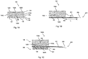
- Figure 1A illustrates a substrate 100 (e.g., a printed circuit board (PCB)), which includes one or more dielectric layers 101 and electrically conductive features (e.g., metal lines and vias) formed in the one or more dielectric layers 101.
- the electrically conductive features are formed in one or more metal layers of the substrate.
- the substrate 100 may also include solder resist layers 105 on the upper surface and the lower surface of the one or more dielectric layers 101.
- the one or more dielectric layers 101 may be formed of any suitable dielectric material, such as resin or fiber glass.
- suitable dielectric material such as resin or fiber glass.
- BT bismaleimide triazine
- FR-4 a composite material composed of woven fiberglass cloth with an epoxy resin binder that is flame resistant
- ceramic, glass, plastic, tape, film, or other supporting materials may be used as the dielectric material of the one or more dielectric layers 101.
- the substrate 100 includes at least one antenna (e.g., 103A) and is designed for radio frequency (RF) applications.
- the one or more dielectric layers 101 may be formed using low-loss high frequency materials such as a woven glass reinforced hydrocarbon/ceramic, or polytetrafluoroethylene (PTFE).
- PTFE polytetrafluoroethylene
- Example dielectric materials include Rogers 400C, 4350, 3003 from Rogers Corporation, Mitsubishi HL972LF, HL970LF from Mitsubishi, or Panasonic Megtron Series from Panasonic.
- Each of the dielectric layers 101 may have a thickness between, e.g., about 50 ⁇ m and about 400 ⁇ m, although other suitable thickness may also be used.
- the conductive features 103 (e.g., 103L, 103V, 103G, 103A, 103B) of the substrate 100 include conductive lines (e.g., copper lines) and vias (e.g., copper vias) formed using a suitable formation method,.
- conductive lines e.g., copper lines
- vias e.g., copper vias
- copper may be deposited over a dielectric layer to form a metal layer, and the deposited metal layer is then patterned to form metal lines.
- openings or recesses may be formed in a dielectric layer, and copper is formed in the openings or recesses to form conductive features such as vias.
- copper is used as an example of the material for forming the conductive features, with the understanding that other suitable conductive materials, such as aluminum, tungsten, cobalt, gold, silver, combinations thereof, alloys thereof, or the like, may also be used to form the various conductive features.
- the number of metal layers in the substrate 100 may be between, e.g., 2 and 10, although other numbers of metal layers are also possible.
- the configuration of the substrate 100 e.g., the locations and interconnections of the conductive features 103) illustrated in Figure 1A (or other figures) is simply an example and not limiting. Depending on the design of the substrate 100, other configurations of the substrate 100 are also possible and are fully intended to be included within the scope of the present disclosure.
- the conductive features of the substrate 100 include conductive lines 103L and vias 103V.
- the via 103V illustrated in Figure 1 (e.g., proximate to the lower surface of the substrate 100) is electrically coupled to an RF terminal (e.g., 303R) of an RFIC 300 in subsequent processing (see Figure 1C).
- Figure 1A further illustrates an antenna 103A (e.g., a copper patch antenna) proximate to the upper surface of the substrate 100, and a ground plane 103G between the antenna 103A and the conductive line 103L.
- the ground plane 103G is a copper plane electrically coupled to a reference voltage level, such as electrical ground, in some embodiments.
- the ground plane 103G has an opening 106 (e.g., a through-hole) disposed between the antenna 103A and the conductive line 103L.
- Figure 1A further illustrates conductive patterns 103B disposed in a same metal layer with the antenna 103A, which conductive patterns 103B may be additional antennas.
- the substrate 100 may have two or more antennas for transmitting and receiving RF signals at the same time.
- Figure 1A illustrates conductive features 104 (e.g., copper pads) formed in the solder resist layer 105 at the lower surface of the substrate 100.
- the conductive features 104 are used for bonding with the flexible circuit 200 in subsequent processing (see Figure 1B ), and are formed by, e.g., forming openings in the solder resist layer 105, then plating a conductive material (e.g., copper) in the openings, in some embodiments.
- the conductive features 104 are electrically coupled to the conductive features 103 of the substrate 100.
- a flexible circuit 200 is attached to the lower surface of the substrate 100.
- the flexible circuit 200 includes a cable 201 and a connector 203 (e.g., an electrical connector) at the end of the cable 201.
- the cable 201 includes one or more conductive layers (e.g., copper layers) formed in a suitable dielectric material such as polyimide.
- Example dielectric materials for the flexible circuit 200 include Pyralux AP or Pyralux LF Coverlay from DuPont.
- the connectors 203 are used for electrical connection to another workpiece (e.g., another PCB, another electrical component). Note that while the flexible circuit 200 is flexible (e.g., can be folded, bent, twisted, or the like during normal operation), the substrate 100 is a rigid substrate (e.g., a PCB), which does not change its shape or dimension under normal working conditions.
- a first portion (may also be referred to as a first segment) of the flexible circuit 200 is disposed within lateral extents of the substrate 100, and a second portion (may also be referred to as a second segment) of the flexible circuit 200 is disposed outside the lateral extents of the substrate 100.
- the first portion of the flexible circuit 200 is disposed between opposing sidewalls of the substrate 100
- the second portion of the flexible circuit 200 is disposed beyond the opposing sidewalls of the substrate 100.
- the portion of cable 201 of the flexible circuit 200 that is disposed beyond opposing sidewalls of the substrate 100 has a length L between about 0.5 mm and about 10 mm, such as between about 0.5 mm and about 5 mm. In other embodiments, the length L is more than 10 mm, depending on, e.g., the design and/or the application of the device.
- the portion of cable 201 of the flexible circuit 200 that is disposed beyond opposing sidewalls of the substrate 100 has a width between about 0.2 mm and about 5 mm. In other embodiments, the width is more than 5 mm, e.g. about 10 mm or more, depending on, e.g., the design and/or the application of the device.
- the first portion of the flexible circuit 200 has conductive features (e.g., copper pads, not shown) that are exposed at the upper surface of the cable 201.
- the flexible circuit 200 may be attached to the lower surface of the substrate 100 by direct metal-to-metal bonding.
- the conductive features 104 of the substrate 100 and the exposed conductive features of the flexible circuit 200 are bonded together by a direct metal-to-metal bonding process.
- the flexible circuit 200 is mechanically and electrically coupled to the lower surface of the substrate 100 (e.g., the conductive features 104) using a conductive glue or a conductive paste.
- the conductive features 104 are not formed in the solder resist layer 105, in which case openings (e.g., through-holes) are formed at the lower surface of the substrate 100 that extend through portions of the dielectric layer 101 to expose some of the conductive features 103 (e.g., 103L, 103V) of the substrate 100, and a plating process (e.g., electro-plating or electro-less plating) is performed to fill the openings with a conductive material (e.g., copper), thereby forming conductive patterns (see, e.g., vias 205 in Figure 2B ) that are exposed at the lower surface of the substrate.
- the flexible circuit 200 may then be mechanically and electrically coupled to the conductive patterns at the lower surface of the substrate using a suitable method, such as direct metal-to-metal bonding, conductive glue, or conductive paste.
- a radio frequency integrated circuit (RFIC) 300 is attached to the lower surface of the substrate 100, such that the first portion of the flexible circuit 200 is disposed between the substrate 100 and the RFIC 300.
- the RFIC 300 is an integrated circuit (may also be referred to as an IC die) that comprises an RF circuit (e.g., a circuit designed for processing radio frequency signals).
- the RFIC 300 may additionally include other circuits, such as a baseband processing circuit.
- the RFIC 300 is electrically coupled to the flexible circuit 200 and the substrate 100.
- the semiconductor structure illustrated in Figure 1C which includes the substrate 100, the flexible circuit 200, and the RFIC 300, is referred to as an AiP device 500A with embedded flexible circuit 200, or an AiP device 500.
- the RFIC 300 includes a semiconductor substrate 301, such as silicon, doped or un-doped, or an active layer of a semiconductor-on-insulator (SOI) substrate.
- the semiconductor substrate may include other semiconductor materials, such as germanium; a compound semiconductor including silicon carbide, gallium arsenic, gallium phosphide, gallium nitride, indium phosphide, indium arsenide, and/or indium antimonide; an alloy semiconductor including SiGe, GaAsP, AlInAs, AlGaAs, GaInAs, GaInP, and/or GaInAsP; or combinations thereof.
- Other substrates such as multi-layered or gradient substrates, may also be used.
- Devices such as transistors, diodes, capacitors, resistors, etc.
- Die connectors 303 e.g., copper pillars
- the RFIC 300 are formed at a front side of the RFIC 300 and provide electrical connection to the circuits of the RFIC 300.
- the RFIC 300 includes a base-band module 311, an RF module 313, a Tx module 315, and an Rx module 317.
- the base-band module 311 is designed to perform digital base-band processing functions, such as digital filtering, equalization, digital re-sampling, or the like.
- the RF module 313 is designed to handle RF signals and perform RF related functions, such as modulating or demodulating RF signals.
- the RF module 313 may include RF related components such as mixers, oscillators, or the like.
- analog-to-digital converters ADCs
- DACs digital-to-analog converters
- the Tx module 315 is designed to perform functions related with transmitting RF signals, and may include electrical components such as power amplifiers.
- the Rx module 3157 is designed to perform functions related with receiving RF signals, and may include electrical components such as analog filters, lower-noise amplifiers, or the like.
- the RFIC 300 is electrically coupled to external circuits through die connectors 303.
- Figure 1D further illustrates RF terminals 303R (e.g., die connectors connected to the Tx or Rx modules) which are electrically coupled to the Tx module 315 and/or to the Rx module 317.
- the RFIC 300 includes the Tx module 315 but does not include the Rx module 317. In other embodiments, the RFIC 300 includes the Rx module 317 and does not include the Tx module 315.
- one or more opening is formed in the cable 201 to expose at least portions of the conductive features 104, and the die connectors 303 extend through the opening(s) to connect with the conductive features 104 (e.g., using a soldering process), in some embodiments.
- the RFIC 300 is connected to the conductive feature(s) 104 of the substrate through the flexible circuit.
- some of the die connectors 303 e.g., the RF terminal 303R
- are coupled to conductive features e.g., the via 103V exposed at the lower surface of the substrate 100.
- openings maybe formed that extend through the cable 201, the solder resist layer 105, and portions of the dielectric layer 101 to expose some conductive features 103 of the substrate 100, and a plating process may be performed to fill the openings with a conductive material to form vias.
- the RFIC 300 may then be bonded to the vias using, e.g., solder.
- solder e.g., solder
- an RF terminal 303R of the RFIC 300 which is configured to send or receive RF signals, is electrically coupled to the conductive features (e.g., 103V and 103L) of the substrate 100.
- the RF signal generated by the RFIC 300 is electrically coupled to the conductive features 103L through the via 103V and the RF terminal 303R.
- the conductive feature 103L radiates the RF signal, which travels through the opening 106 and is electromagnetically coupled to the antenna 103A.
- the RF signal is then transmitted by the antenna 103A.
- the antenna 103A is a receive antenna
- the antenna 103A picks up the RF signal (e.g., through electromagnetic coupling), the received RF signal is then electromagnetically coupled to the RF terminal 303R, e.g., through the opening 106 and the conductive features 103L/103V.
- electrical connection between the RFIC 300 and external circuits is achieved by the connector 203 of the flexible circuit 200.
- the connector 203 may have a plurality of connection pins, a plurality of conductive pads, or the like, to provide electrical connection for multiple signals.
- a plurality of external connectors e.g., solder bumps, conductive pillars
- FIGS 2A-2C illustrate cross-sectional views of an AiP device 500B with embedded flexible circuit 200 at various stages of fabrication, in accordance with an embodiment.
- the formation process of the AiP device 500B is similar to that of AiP device 500A, but the substrate 100 in Figure 2A does not have conductive features (e.g., 104 in Figure 1A ) exposed at the lower surface of the substrate 100.
- the substrate 100 in Figure 2A does not have the solder resist layer 105 at the lower surface of the substrate 100.
- the flexible circuit 200 is attached to the substrate 100 using a dielectric-to-dielectric bonding process.
- the high temperature and the high pressure of the dielectric-to-dielectric bonding process bond the dielectric material (e.g., polyimide) of the flexible circuit 200 with the dielectric material (e.g., woven glass reinforced hydrocarbon/ceramic, or PTFE) of the substrate 100, thereby bonding the flexible circuit 200 to the substrate 100.
- the dielectric material e.g., polyimide
- the dielectric material e.g., woven glass reinforced hydrocarbon/ceramic, or PTFE
- openings are formed in the flexible circuit 200 using, e.g., a laser drilling process or an etching process.
- the openings extends through the flexible circuit 200 and a portion of the dielectric layer 101 of the substrate 100 to expose some of the conductive features 130 (e.g., 130L) of the substrate 100.
- a plating process e.g., an electro-plating process or an electroless plating process
- a conductive material e.g., copper
- the openings are formed to extend through conductive regions (e.g., copper regions) of the flexible circuit 200, and therefore, the vias 205, once formed, are electrically coupled to the flexible circuit 200.
- the openings are formed in regions of the flexible circuit 200 that do not have conductive features, and therefore, the vias 205 extend through dielectric regions (e.g., polyimide regions) of the cable 201.
- an optional solder resist layer 105 may be formed on the lower surface of the flexible circuit 200 (see Figure 2C ).
- the RFIC 300 is attached to the lower surface of the substrate 100, thereby forming the AiP device 500B with embedded flexible circuit.
- openings are formed that extend through the solder resist layer 105 (if formed) to expose the vias 205.
- the openings may also extend partially through the dielectric material of the flexible circuit 200 to expose conductive features of the flexible circuit 200.
- the die connectors 303/303R of the RFIC 300 extend through the openings and are bonded (e.g., using solder) to the vias 205 and/or the exposed conductive features of the flexible circuit 200, in some embodiments.
- Figures 3A-3C illustrate cross-sectional views of an AiP device 500C with embedded flexible circuit 200 at various stages of fabrication, in accordance with an embodiment.
- the formation process of the AiP device 500C is similar to that of AiP device 500B, but the substrate 100 in Figure 3A includes an upper portion 100U and a lower portion 100L.
- the flexible circuit 200 is laminated between the upper portion 100U and the lower portion 100L.
- the upper surface of the flexible circuit 200 is attached to a lower surface 100S1 of the upper portion 100U of the substrate 100, and the lower surface of the flexible circuit 200 is attached to an upper surface 100S2 of the lower portion 100L.
- the flexible circuit 200 may be attached to the upper portion 100U and the lower portion 100L using any suitable method such as direct metal-to-metal bonding, dielectric-to-dielectric bonding, conductive paste, conductive glues, or the like, similar to the processes discussed above for the AiP devices 500A and 500B.
- a drilling process may be performed to form openings in the upper portion 100U and/or the lower portion 100L, and a plating process may be performed to fill the openings with a conductive material (e.g., copper) to form conductive features in the upper portion 100U and/or the lower portion 100L for electrically connection with the flexible circuit 200, similar to the process discussed above for the AiP device 500B.
- a conductive material e.g., copper
- Figure 3B illustrates the substrate 100 with embedded flexible circuit 200, after the processing of Figure 3A is finished.
- the upper portion 100U and the lower portion 100L are joined together and form a single substrate 100, with the flexible circuit 200 laminated in between.
- the flexible circuit 200 is electrically coupled to the substrate 100, and may function as a middle metal layer of the substrate 100.
- the RFIC 300 is attached to the lower surface of the substrate 100, and is electrically coupled to the substrate 100 and the flexible circuit 200, thereby forming the AiP device 500C.
- the RFIC 300 may be attached by forming openings in the solder resist layer 105 to expose conductive features 103 of the substrate 100, and bonding the die connectors 303/303R of the RFIC 300 to the exposed conductive features 103.
- FIGS 4A-4D illustrate various views (e.g., cross-sectional views, top view) of an AiP device 500D with embedded flexible circuit at various stages of fabrication, in accordance with an embodiment.
- the formation process of the AiP device 500D is similar to that of AiP device 500B, but the flexible circuit 200 is attached to the upper surface of the substrate 100.
- the antenna 103A is at the upper surface of the substrate 100.
- the flexible circuit 200 is attached to the upper surface of the substrate 100 using any suitable methods, such as those discussed above for the AiP devices 500A, 500B, and 500C.
- Figure 4B shows the substrate 100 with the flexible circuit 200 attached.
- the flexible circuit 200 is electrically coupled to the substrate 100 after being attached.
- a solder resist layer 105 is formed over the upper surface of the flexible circuit 200. In other embodiments, the solder resist layer 105 is omitted.
- the RFIC 300 is mechanically and electrically coupled to the lower surface of the substrate 100, using any suitable method, such as the process described above for the AiP device 500C of Figure 3C , thereby forming the AiP device 500D.
- the RFIC 300 is also electrically coupled to the flexible circuit 200 through the metal layers of the substrate 100.
- Figure 4D illustrates a top view of the AiP device 500D along cross-section A-A in Figure 4C .
- the flexible circuit 200 has an opening 202 which exposes the underlying antennas 103A.
- the opening 202 in the flexible circuit 200 of Figure 4D may be omitted in other embodiments, such as the AiP devices 500A, 500B, or 500C, because in those embodiments, the flexible circuit 200 is disposed between the antenna 103A and the RFIC 300 and therefore, may not interfere with the transmission and/or reception of RF signals by the antenna 103A.
- the antenna 103A is formed in a topmost metal layer (e.g., a metal layer furthest from the RFIC 300) of the substrate 100, while the flexible circuit 200 is proximate to a bottommost metal layer (e.g., a metal layer closest to the RFIC 300) of the substrate 100.
- Figure 4D also illustrates conductive features 215 (e.g., copper lines, vias) formed in the flexible circuit 200, which are connected to the connector 203 (see Figure 4C ) and are used for electrical connection between the RFIC 300 and another PCB board or other electrical component.
- conductive features 215 e.g., copper lines, vias
- Figure 5A is a cross-sectional view illustrating the electrical connection between an embodiment antenna-in-package (AiP) device 500 (e.g., 500A, 500B, 500C, or 500D) and another electrical component inside an electronic device 400, in an embodiment.
- the electronic device 400 maybe a cell phone, a tablet, a laptop, a speaker, a home assistant device, a TV set, or the like.
- the electronic device 400 is a cell phone with a front side 401 (e.g., with an LCD display), a back side 403, and a bezel 405 between the front side 401 and the back side 403.
- Figure 5A also illustrates electrical components 411 and 413 (e.g., PCBs) inside the electronic device 400.
- the connector 203 of the flexible circuit 200 of the AiP device 500 is a surface-mount type of connector, and is connected to the electrical component 413 using, e.g., a soldering process.
- the flexible circuit 200 allows for flexibility in choosing the location of the AiP device 500 inside the electronic device 400.
- Figure 5B is a cross-sectional view illustrating the electrical connection between an embodiment antenna-in-package (AiP) device 500 (e.g., 500A, 500B, 500C, or 500D) and another electrical component inside an electronic device 400, in another embodiment.
- AiP antenna-in-package
- the embodiment of Figure 5B is similar to that of Figure 5A , but the connector 203 of the flexible circuit 200 of the AiP device 500 in Figure 5B is a plug-in type of connector. Therefore, the connector 203 is connected to the electrical component 413 through an electrical socket.
- FIG. 6A is a cross-sectional view illustrating the location of an embodiment antenna-in-package (AiP) device 500 (e.g., 500A, 500B, 500C, or 500D) inside an electronic device 400, in an embodiment.
- the flexible circuit 200 allows the AiP device 500 to be located at any suitable location within the electronic device 400.
- the flexible circuit 200 allows the AiP device 500 to be placed in the corner region of the cell phone next to the bezel 405, which corner region may provide more space for the AiP device 500.
- the AiP device 500 may be placed at an angle with respect to the cell phone.
- the upper surface 500U of the AiP device 500 may form an angle of, e.g., about 45 degrees with the front side 401 of the electronic device 400.
- FIG. 6B is a cross-sectional view illustrating the location of an embodiment antenna-in-package (AiP) device 500 (e.g., 500A, 500B, 500C, or 500D) inside an electronic device 400, in another embodiment.
- AiP antenna-in-package
- the upper surface 500U of the AiP device 500 forms an angle of 90 degrees with the front side 401 of the electronic device 400.
- Other angles and locations of the AiP device 500 within the mobile device are also possible, and are fully intended to be included within the scope of the present disclosure.
- the flexibility in the location of the AiP device 500, afforded by the disclosed structure of the AiP device 500 makes it easier to fit the AiP device 500 into various mobile devices.
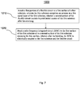
- Figure 7 illustrates a flow chart of a method 1000 of forming an electrical device, in accordance with some embodiments. It should be understood that the embodiment method shown in Figure 7 is merely an example of many possible embodiment methods. One of ordinary skill in the art would recognize many variations, alternatives, and modifications. For example, various steps as illustrated in Figure 7 may be added, removed, replaced, rearranged and repeated.
- the method 1000 may be used to fabricate various AiP devices with embedded flexible circuit, such as the AiP devices 500A, 500B, 500C, or 500D.
- a first portion of a flexible circuit is attached to a first surface (e.g., an upper surface or a lower surface) of a first substrate, wherein the first substrate comprises an antenna in a first metal layer of the first substrate, wherein a second portion of the flexible circuit extends beyond lateral extents of the first substrate after the attaching.
- a radio frequency integrated circuit (e.g., 300) is bonded to the first surface of the first substrate or to a second surface of the first substrate opposing the first surface, wherein after the bonding, the RFIC is electrically coupled to the first substrate and the flexible circuit.
- RFIC radio frequency integrated circuit
- Embodiments may achieve advantages.
- various embodiments disclosed herein form different AiP devices with embedded flexible circuits.
- the electrical connection between the AiP device and an external electrical component is achieved through a connector of the flexible circuit, which obviates the need to form large external connectors, such as solder bumps or conductive pillars on the AiP device. This reduces the height of the AiP device formed, which allows the AiP device to fit into small mobile devices.
- the flexible circuit embedded in the AiP device allows for flexibility in choosing the location of the AiP device within the mobile device, which allows the AiP devices to fit into even smaller mobile devices.
- the flexible circuit 200 is designed for easy integration with the substrate 100 without negatively impacting the RF performance.
- the opening 202 in the flexible circuit 200 allows RF signals to be transmitted and/or received by the antennas 103A without being attenuated or blocked by the flexible circuit.
Landscapes
- Engineering & Computer Science (AREA)
- Microelectronics & Electronic Packaging (AREA)
- Combinations Of Printed Boards (AREA)
Abstract
Description
- The present invention relates generally to semiconductor packages, and, in particular embodiments, to antenna-in-package (AiP) devices.
- Antenna-in-package (AiP) represents a new trend in integrated circuit (IC) packaging which is an enabler of smaller and highly integrated semiconductor devices. An AiP device includes integrated circuits (ICs) (e.g., base-band IC and RF transceiver IC) and an antenna inside a same package. Antenna-in-package allows integration of complex RF components together with base-band circuitry into a self-contained module. AiP devices not only reduce the footprint of the functional modules they integrated, but also facilitate the work of system integrators. For example, the system integrators no longer have to design complex RF circuits at the application printed circuit board (PCB) level. Moreover, the overall size of the complete application is reduced.
- As the form factor of mobile devices continues to shrink, the reduced space inside the mobile devices poses new demands and challenges for the design of semiconductor devices inside the mobile devices, such as AiP devices. For example, as the mobile device becomes thinner, the reduced thickness of the mobile device requires that the height of AiP devices be reduced accordingly. There is a need in the art for improved packaging techniques for semiconductor devices such as AiP devices.
- There may be a demand for providing an improved concept for a semiconductor device and a method of forming an electrical device.
- Such a demand may be satisfied by the subject mater of any of the claims.
- In accordance with an embodiment of the present invention, a semiconductor device includes a substrate comprising an antenna and a conductive feature; an integrated circuit (IC) die attached to the substrate and comprising a radio frequency (RF) circuit; and a flexible circuit integrated with the substrate, where the flexible circuit is electrically coupled to the IC die and the substrate, a first portion of the flexible circuit being disposed between opposing sidewalls of the substrate, a second portion of the flexible circuit extending beyond the opposing sidewalls of the substrate, the second portion of the flexible circuit comprising an electrical connector at a distal end.
- In accordance with an embodiment of the present invention, a semiconductor device includes an integrated circuit (IC) comprising a radio frequency (RF) circuit and an RF terminal configured to transmit or receive RF signals; a substrate comprising an antenna proximate to a first side of the substrate facing away from the IC and comprising a conductive feature proximate to a second side of the substrate facing the IC, wherein the IC is attached to the second side of the substrate, and the RF terminal of the IC is electrically coupled to the conductive feature of the substrate; and a flexible circuit attached to the substrate, wherein the flexible circuit is electrically coupled to the IC and the substrate, wherein a first segment of the flexible circuit is disposed within lateral extents of the substrate, and a second segment of the flexible circuit is disposed outside the lateral extents of the substrate, the second segment of the flexible circuit comprising an electrical connector.
- In accordance with an embodiment of the present invention, a method of forming an electrical device includes attaching a first portion of a flexible circuit to a first substrate, wherein the first substrate comprises an antenna in a first metal layer of the first substrate, wherein a second portion of the flexible circuit extends beyond lateral extents of the first substrate after the attaching, the second portion of the flexible circuit having an electrical connector at a distal end; and bonding a radio frequency integrated circuit (RFIC) to a first surface of the first substrate, wherein after the bonding, the RFIC is electrically coupled to the first substrate and the flexible circuit.
- For a more complete understanding of the present invention, and the advantages thereof, reference is now made to the following descriptions taken in conjunction with the accompanying drawings, in which:
-
Figures 1A-1C illustrate cross-sectional views of an antenna-in-package (AiP) device at various stages of fabrication, in accordance with an embodiment; -
Figure 1D illustrates a functional block diagram of a radio frequency integrated circuit (RFIC), in accordance with an embodiment; -
Figures 2A-2C illustrate cross-sectional views of an antenna-in-package (AiP) device at various stages of fabrication, in accordance with an embodiment; -
Figures 3A-3C illustrate cross-sectional views of an antenna-in-package (AiP) device at various stages of fabrication, in accordance with an embodiment; -
Figures 4A-4D illustrate various views of an antenna-in-package (AiP) device at various stages of fabrication, in accordance with an embodiment; -
Figure 5A is a cross-sectional view illustrating the electrical connection between an antenna-in-package (AiP) device and another electrical component inside an electronic device, in an embodiment; -
Figure 5B is a cross-sectional view illustrating the electrical connection between an antenna-in-package (AiP) device and another electrical component inside an electronic device, in another embodiment; -
Figure 6A is a cross-sectional view illustrating the location of an antenna-in-package (AiP) device inside an electronic device, in an embodiment; -
Figure 6B is a cross-sectional view illustrating the location of an antenna-in-package (AiP) device inside an electronic device, in another embodiment; and -
Figure 7 is a flow chart of a method of forming a semiconductor device, in an embodiment. - The making and using of the presently disclosed embodiments are discussed in detail below. It should be appreciated, however, that the present invention provides many applicable inventive concepts that can be embodied in a wide variety of specific contexts. The specific embodiments discussed are merely illustrative of specific ways to make and use the invention, and do not limit the scope of the invention. Throughout the discussion herein, unless otherwise specified, the same or similar reference numeral in different figures refers to the same or similar component. Further, spatially relative terms, such as "beneath," "below," "lower," "above," "upper" and the like, may be used herein for ease of description to describe one element or feature's relationship to another element(s) or feature(s) as illustrated in the figures. The spatially relative terms are intended to encompass different orientations of the device in use or operation in addition to the orientation depicted in the figures. The apparatus may be otherwise oriented (rotated 90 degrees or at other orientations) and the spatially relative descriptors used herein may likewise be interpreted accordingly.
- The present invention will be described with respect to example embodiments in a specific context, namely antenna-in-package (AiP) devices with embedded flexible circuit. Note that AiP devices are used in the description herein as non-limiting examples. The scope of the present invention includes semiconductor devices other than AiP devices. For instance, such devices differ from an AiP device in that the one or more antennas they comprise are not located within their substrate, but on one or more outer surface thereof. In other words, non-AiP semiconductor devices with embedded flexible circuit are also included within the scope of the present disclosure. For example, the AiP device in the various disclosed embodiments herein may be replaced by another semiconductor device (e.g., a non-AiP device) that has a multi-layered structure. These and other variations are fully intended to be included within the scope of the present disclosure.
- In embodiments of the present invention, a flexible circuit is attached to a substrate such that a first portion of the flexible circuit is within lateral extents of the substrate and a second portion of the flexible circuit is outside the lateral extents of the substrate. The substrate has one or more antennas formed in a metal layer of the substrate. The flexible circuit is electrically coupled to conductive features of the substrate. The second portion of the flexible circuit has an electrical connector for connection with an external circuit. A radio-frequency integrated circuit (RFIC) is bonded to the substrate, and is electrically coupled to the flexible circuit and the substrate. Electrical connections between the RFIC and external circuits are achieved through the electrical connector of the flexible circuit. RF signals are transmitted from or received by the RFIC using the one or more antennas in the substrate, which one or more antennas are electromagnetically coupled to an RF terminal of the RFIC. The substrate, with the flexible circuit and the RFIC attached, form an AiP device with embedded flexible circuit. The disclosed embodiments reduce the height of the AiP device formed, which allows the AiP device to be embedded in various positions and at various angles within the bezel of a mobile device, in some embodiments.
- Referring now to
Figures 1A-1C , which illustrate cross-sectional views of anAiP device 500A at various stages of fabrication, in accordance with an embodiment.Figure 1A illustrates a substrate 100 (e.g., a printed circuit board (PCB)), which includes one or moredielectric layers 101 and electrically conductive features (e.g., metal lines and vias) formed in the one or moredielectric layers 101. The electrically conductive features are formed in one or more metal layers of the substrate. Thesubstrate 100 may also includesolder resist layers 105 on the upper surface and the lower surface of the one or moredielectric layers 101. - The one or more
dielectric layers 101 may be formed of any suitable dielectric material, such as resin or fiber glass. For example, bismaleimide triazine (BT) resin, FR-4 (a composite material composed of woven fiberglass cloth with an epoxy resin binder that is flame resistant), ceramic, glass, plastic, tape, film, or other supporting materials may be used as the dielectric material of the one or moredielectric layers 101. In the illustrated embodiment, thesubstrate 100 includes at least one antenna (e.g., 103A) and is designed for radio frequency (RF) applications. Accordingly, the one or moredielectric layers 101 may be formed using low-loss high frequency materials such as a woven glass reinforced hydrocarbon/ceramic, or polytetrafluoroethylene (PTFE). Example dielectric materials include Rogers 400C, 4350, 3003 from Rogers Corporation, Mitsubishi HL972LF, HL970LF from Mitsubishi, or Panasonic Megtron Series from Panasonic. Each of thedielectric layers 101 may have a thickness between, e.g., about 50 µm and about 400 µm, although other suitable thickness may also be used. - The conductive features 103 (e.g., 103L, 103V, 103G, 103A, 103B) of the
substrate 100 include conductive lines (e.g., copper lines) and vias (e.g., copper vias) formed using a suitable formation method,. For example, copper may be deposited over a dielectric layer to form a metal layer, and the deposited metal layer is then patterned to form metal lines. As another example, openings or recesses may be formed in a dielectric layer, and copper is formed in the openings or recesses to form conductive features such as vias. Throughout the description herein, copper is used as an example of the material for forming the conductive features, with the understanding that other suitable conductive materials, such as aluminum, tungsten, cobalt, gold, silver, combinations thereof, alloys thereof, or the like, may also be used to form the various conductive features. Depending on the design of thesubstrate 100, the number of metal layers in thesubstrate 100 may be between, e.g., 2 and 10, although other numbers of metal layers are also possible. The configuration of the substrate 100 (e.g., the locations and interconnections of the conductive features 103) illustrated inFigure 1A (or other figures) is simply an example and not limiting. Depending on the design of thesubstrate 100, other configurations of thesubstrate 100 are also possible and are fully intended to be included within the scope of the present disclosure. - In the example of
Figure 1A , the conductive features of thesubstrate 100 includeconductive lines 103L and vias 103V. The via 103V illustrated inFigure 1 (e.g., proximate to the lower surface of the substrate 100) is electrically coupled to an RF terminal (e.g., 303R) of anRFIC 300 in subsequent processing (seeFigure 1C). Figure 1A further illustrates anantenna 103A (e.g., a copper patch antenna) proximate to the upper surface of thesubstrate 100, and aground plane 103G between theantenna 103A and theconductive line 103L. Theground plane 103G is a copper plane electrically coupled to a reference voltage level, such as electrical ground, in some embodiments. InFigure 1A , theground plane 103G has an opening 106 (e.g., a through-hole) disposed between theantenna 103A and theconductive line 103L.Figure 1A further illustratesconductive patterns 103B disposed in a same metal layer with theantenna 103A, whichconductive patterns 103B may be additional antennas. For example, thesubstrate 100 may have two or more antennas for transmitting and receiving RF signals at the same time. - In addition,
Figure 1A illustrates conductive features 104 (e.g., copper pads) formed in the solder resistlayer 105 at the lower surface of thesubstrate 100. The conductive features 104 are used for bonding with theflexible circuit 200 in subsequent processing (seeFigure 1B ), and are formed by, e.g., forming openings in the solder resistlayer 105, then plating a conductive material (e.g., copper) in the openings, in some embodiments. Although not illustrated inFigure 1A , theconductive features 104 are electrically coupled to theconductive features 103 of thesubstrate 100. - Next, in
Figure 1B , aflexible circuit 200 is attached to the lower surface of thesubstrate 100. Theflexible circuit 200 includes acable 201 and a connector 203 (e.g., an electrical connector) at the end of thecable 201. Thecable 201 includes one or more conductive layers (e.g., copper layers) formed in a suitable dielectric material such as polyimide. Example dielectric materials for theflexible circuit 200 include Pyralux AP or Pyralux LF Coverlay from DuPont. Theconnectors 203 are used for electrical connection to another workpiece (e.g., another PCB, another electrical component). Note that while theflexible circuit 200 is flexible (e.g., can be folded, bent, twisted, or the like during normal operation), thesubstrate 100 is a rigid substrate (e.g., a PCB), which does not change its shape or dimension under normal working conditions. - As illustrated in
Figure 1B , a first portion (may also be referred to as a first segment) of theflexible circuit 200 is disposed within lateral extents of thesubstrate 100, and a second portion (may also be referred to as a second segment) of theflexible circuit 200 is disposed outside the lateral extents of thesubstrate 100. In other words, the first portion of theflexible circuit 200 is disposed between opposing sidewalls of thesubstrate 100, and the second portion of theflexible circuit 200 is disposed beyond the opposing sidewalls of thesubstrate 100. In some embodiments, the portion ofcable 201 of theflexible circuit 200 that is disposed beyond opposing sidewalls of thesubstrate 100 has a length L between about 0.5 mm and about 10 mm, such as between about 0.5 mm and about 5 mm. In other embodiments, the length L is more than 10 mm, depending on, e.g., the design and/or the application of the device. - In some embodiments, the portion of
cable 201 of theflexible circuit 200 that is disposed beyond opposing sidewalls of thesubstrate 100 has a width between about 0.2 mm and about 5 mm. In other embodiments, the width is more than 5 mm, e.g. about 10 mm or more, depending on, e.g., the design and/or the application of the device. - In some embodiments, the first portion of the
flexible circuit 200 has conductive features (e.g., copper pads, not shown) that are exposed at the upper surface of thecable 201. Theflexible circuit 200 may be attached to the lower surface of thesubstrate 100 by direct metal-to-metal bonding. In other words, theconductive features 104 of thesubstrate 100 and the exposed conductive features of theflexible circuit 200 are bonded together by a direct metal-to-metal bonding process. In other embodiments, theflexible circuit 200 is mechanically and electrically coupled to the lower surface of the substrate 100 (e.g., the conductive features 104) using a conductive glue or a conductive paste. In yet other embodiments, theconductive features 104 are not formed in the solder resistlayer 105, in which case openings (e.g., through-holes) are formed at the lower surface of thesubstrate 100 that extend through portions of thedielectric layer 101 to expose some of the conductive features 103 (e.g., 103L, 103V) of thesubstrate 100, and a plating process (e.g., electro-plating or electro-less plating) is performed to fill the openings with a conductive material (e.g., copper), thereby forming conductive patterns (see, e.g., vias 205 inFigure 2B ) that are exposed at the lower surface of the substrate. Theflexible circuit 200 may then be mechanically and electrically coupled to the conductive patterns at the lower surface of the substrate using a suitable method, such as direct metal-to-metal bonding, conductive glue, or conductive paste. - Next, in
Figure 1C , a radio frequency integrated circuit (RFIC) 300 is attached to the lower surface of thesubstrate 100, such that the first portion of theflexible circuit 200 is disposed between thesubstrate 100 and theRFIC 300. TheRFIC 300 is an integrated circuit (may also be referred to as an IC die) that comprises an RF circuit (e.g., a circuit designed for processing radio frequency signals). TheRFIC 300 may additionally include other circuits, such as a baseband processing circuit. After being attached, theRFIC 300 is electrically coupled to theflexible circuit 200 and thesubstrate 100. The semiconductor structure illustrated inFigure 1C , which includes thesubstrate 100, theflexible circuit 200, and theRFIC 300, is referred to as anAiP device 500A with embeddedflexible circuit 200, or anAiP device 500. - As illustrated in
Figure 1C , theRFIC 300 includes asemiconductor substrate 301, such as silicon, doped or un-doped, or an active layer of a semiconductor-on-insulator (SOI) substrate. The semiconductor substrate may include other semiconductor materials, such as germanium; a compound semiconductor including silicon carbide, gallium arsenic, gallium phosphide, gallium nitride, indium phosphide, indium arsenide, and/or indium antimonide; an alloy semiconductor including SiGe, GaAsP, AlInAs, AlGaAs, GaInAs, GaInP, and/or GaInAsP; or combinations thereof. Other substrates, such as multi-layered or gradient substrates, may also be used. Devices, such as transistors, diodes, capacitors, resistors, etc., may be formed in and/or on thesemiconductor substrate 301 and may be interconnected by interconnect structures formed by, for example, metallization patterns in one or more dielectric layers over thesemiconductor substrate 301 to form an integrated circuit. Die connectors 303 (e.g., copper pillars) of theRFIC 300 are formed at a front side of theRFIC 300 and provide electrical connection to the circuits of theRFIC 300. - Referring temporarily to
Figure 1D , which illustrates a functional block diagram of theRFIC 300, in an embodiment. Note that for simplicity, not all functional blocks of theRFIC 300 are illustrated inFigure 1D . In the example ofFigure 1D , theRFIC 300 includes a base-band module 311, anRF module 313, aTx module 315, and anRx module 317. The base-band module 311 is designed to perform digital base-band processing functions, such as digital filtering, equalization, digital re-sampling, or the like. TheRF module 313 is designed to handle RF signals and perform RF related functions, such as modulating or demodulating RF signals. TheRF module 313 may include RF related components such as mixers, oscillators, or the like. Depending on the design of theRFIC 300, analog-to-digital converters (ADCs) and/or digital-to-analog converters (DACs) maybe formed in theRF module 313 or in the base-band module 311. TheTx module 315 is designed to perform functions related with transmitting RF signals, and may include electrical components such as power amplifiers. The Rx module 3157 is designed to perform functions related with receiving RF signals, and may include electrical components such as analog filters, lower-noise amplifiers, or the like. TheRFIC 300 is electrically coupled to external circuits throughdie connectors 303.Figure 1D further illustratesRF terminals 303R (e.g., die connectors connected to the Tx or Rx modules) which are electrically coupled to theTx module 315 and/or to theRx module 317. In some embodiments, theRFIC 300 includes theTx module 315 but does not include theRx module 317. In other embodiments, theRFIC 300 includes theRx module 317 and does not include theTx module 315. These and other variations are fully intended to be included within the scope of the present disclosure. - Referring back to
Figure 1C , to attach theRFIC 300 to thesubstrate 100, one or more opening (e.g., through-holes) is formed in thecable 201 to expose at least portions of theconductive features 104, and thedie connectors 303 extend through the opening(s) to connect with the conductive features 104 (e.g., using a soldering process), in some embodiments. In other words, theRFIC 300 is connected to the conductive feature(s) 104 of the substrate through the flexible circuit. In the illustrated example, some of the die connectors 303 (e.g., theRF terminal 303R) are coupled to conductive features (e.g., the via 103V) exposed at the lower surface of thesubstrate 100. In embodiments where theconductive features 104 are not formed, openings maybe formed that extend through thecable 201, the solder resistlayer 105, and portions of thedielectric layer 101 to expose someconductive features 103 of thesubstrate 100, and a plating process may be performed to fill the openings with a conductive material to form vias. TheRFIC 300 may then be bonded to the vias using, e.g., solder. Besides the above descripted methods to attach theRFIC 300 to thesubstrate 100, other methods are also possible and are fully intended to be included within the scope of the present disclosure. - In the example of
Figure 1C , an RF terminal 303R of theRFIC 300, which is configured to send or receive RF signals, is electrically coupled to the conductive features (e.g., 103V and 103L) of thesubstrate 100. In embodiments where theantenna 103A is a transmission antenna, the RF signal generated by theRFIC 300 is electrically coupled to the conductive features 103L through the via 103V and theRF terminal 303R. Theconductive feature 103L radiates the RF signal, which travels through theopening 106 and is electromagnetically coupled to theantenna 103A. The RF signal is then transmitted by theantenna 103A. In embodiments where theantenna 103A is a receive antenna, theantenna 103A picks up the RF signal (e.g., through electromagnetic coupling), the received RF signal is then electromagnetically coupled to theRF terminal 303R, e.g., through theopening 106 and the conductive features 103L/103V. - Note that in the example of
Figure 1C , electrical connection between theRFIC 300 and external circuits, such as another PCB or other electrical component, is achieved by theconnector 203 of theflexible circuit 200. Theconnector 203 may have a plurality of connection pins, a plurality of conductive pads, or the like, to provide electrical connection for multiple signals. As a result of using theflexible circuit 200 for the electrical connection between theRFIC 300 and external circuits, there is no need to form a plurality of external connectors (e.g., solder bumps, conductive pillars) at the lower surface of thesubstrate 100. This advantageously reduces the height of theAiP device 500A, which allows theAiP device 500A to be used in applications where the height available for the AiP device is limited (seeFigures 5A, 5B ,6A, and 6B and related discussions hereinafter). -
Figures 2A-2C illustrate cross-sectional views of anAiP device 500B with embeddedflexible circuit 200 at various stages of fabrication, in accordance with an embodiment. The formation process of theAiP device 500B is similar to that ofAiP device 500A, but thesubstrate 100 inFigure 2A does not have conductive features (e.g., 104 inFigure 1A ) exposed at the lower surface of thesubstrate 100. In addition, thesubstrate 100 inFigure 2A does not have the solder resistlayer 105 at the lower surface of thesubstrate 100. - Referring to
Figure 2A , theflexible circuit 200 is attached to thesubstrate 100 using a dielectric-to-dielectric bonding process. The high temperature and the high pressure of the dielectric-to-dielectric bonding process bond the dielectric material (e.g., polyimide) of theflexible circuit 200 with the dielectric material (e.g., woven glass reinforced hydrocarbon/ceramic, or PTFE) of thesubstrate 100, thereby bonding theflexible circuit 200 to thesubstrate 100. - Next, in
Figure 2B , openings (e.g., through-holes) are formed in theflexible circuit 200 using, e.g., a laser drilling process or an etching process. The openings extends through theflexible circuit 200 and a portion of thedielectric layer 101 of thesubstrate 100 to expose some of the conductive features 130 (e.g., 130L) of thesubstrate 100. Next, a plating process (e.g., an electro-plating process or an electroless plating process) is performed to fill the openings with a conductive material (e.g., copper) to form conductive features, such asvias 205. In some embodiments, the openings are formed to extend through conductive regions (e.g., copper regions) of theflexible circuit 200, and therefore, thevias 205, once formed, are electrically coupled to theflexible circuit 200. In some embodiments, the openings are formed in regions of theflexible circuit 200 that do not have conductive features, and therefore, thevias 205 extend through dielectric regions (e.g., polyimide regions) of thecable 201. Next, an optional solder resistlayer 105 may be formed on the lower surface of the flexible circuit 200 (seeFigure 2C ). - Next, in
Figure 2C , theRFIC 300 is attached to the lower surface of thesubstrate 100, thereby forming theAiP device 500B with embedded flexible circuit. To attach theRFIC 300, openings are formed that extend through the solder resist layer 105 (if formed) to expose thevias 205. The openings may also extend partially through the dielectric material of theflexible circuit 200 to expose conductive features of theflexible circuit 200. Thedie connectors 303/303R of theRFIC 300 extend through the openings and are bonded (e.g., using solder) to thevias 205 and/or the exposed conductive features of theflexible circuit 200, in some embodiments. -
Figures 3A-3C illustrate cross-sectional views of anAiP device 500C with embeddedflexible circuit 200 at various stages of fabrication, in accordance with an embodiment. The formation process of theAiP device 500C is similar to that ofAiP device 500B, but thesubstrate 100 inFigure 3A includes an upper portion 100U and alower portion 100L. Theflexible circuit 200 is laminated between the upper portion 100U and thelower portion 100L. - As illustrated in
Figure 3A , the upper surface of theflexible circuit 200 is attached to a lower surface 100S1 of the upper portion 100U of thesubstrate 100, and the lower surface of theflexible circuit 200 is attached to an upper surface 100S2 of thelower portion 100L. Depending on whether there are conductive features exposed at the lower surface 100S1 or at the upper surface 100S2, theflexible circuit 200 may be attached to the upper portion 100U and thelower portion 100L using any suitable method such as direct metal-to-metal bonding, dielectric-to-dielectric bonding, conductive paste, conductive glues, or the like, similar to the processes discussed above for theAiP devices lower portion 100L, and a plating process may be performed to fill the openings with a conductive material (e.g., copper) to form conductive features in the upper portion 100U and/or thelower portion 100L for electrically connection with theflexible circuit 200, similar to the process discussed above for theAiP device 500B. -
Figure 3B illustrates thesubstrate 100 with embeddedflexible circuit 200, after the processing ofFigure 3A is finished. As illustrated inFigure 3B , the upper portion 100U and thelower portion 100L are joined together and form asingle substrate 100, with theflexible circuit 200 laminated in between. Theflexible circuit 200 is electrically coupled to thesubstrate 100, and may function as a middle metal layer of thesubstrate 100. - Next, in
Figure 3C , theRFIC 300 is attached to the lower surface of thesubstrate 100, and is electrically coupled to thesubstrate 100 and theflexible circuit 200, thereby forming theAiP device 500C. TheRFIC 300 may be attached by forming openings in the solder resistlayer 105 to exposeconductive features 103 of thesubstrate 100, and bonding thedie connectors 303/303R of theRFIC 300 to the exposed conductive features 103. -
Figures 4A-4D illustrate various views (e.g., cross-sectional views, top view) of anAiP device 500D with embedded flexible circuit at various stages of fabrication, in accordance with an embodiment. The formation process of theAiP device 500D is similar to that ofAiP device 500B, but theflexible circuit 200 is attached to the upper surface of thesubstrate 100. - In
Figure 4A , theantenna 103A is at the upper surface of thesubstrate 100. Theflexible circuit 200 is attached to the upper surface of thesubstrate 100 using any suitable methods, such as those discussed above for theAiP devices -
Figure 4B shows thesubstrate 100 with theflexible circuit 200 attached. Theflexible circuit 200 is electrically coupled to thesubstrate 100 after being attached. Next, a solder resistlayer 105 is formed over the upper surface of theflexible circuit 200. In other embodiments, the solder resistlayer 105 is omitted. - Next, in
Figure 4C , theRFIC 300 is mechanically and electrically coupled to the lower surface of thesubstrate 100, using any suitable method, such as the process described above for theAiP device 500C ofFigure 3C , thereby forming theAiP device 500D. TheRFIC 300 is also electrically coupled to theflexible circuit 200 through the metal layers of thesubstrate 100. -
Figure 4D illustrates a top view of theAiP device 500D along cross-section A-A inFigure 4C . For simplicity, not all features of theAiP device 500D are shown. As illustrated inFigure 4D , theflexible circuit 200 has anopening 202 which exposes theunderlying antennas 103A. In other words, there is no metal region in theflexible circuit 200 that is disposed over (e.g., directly over) theantennas 103A, such that transmission and/or reception of RF signals by theantennas 103A may be performed without being blocked or attenuated. Note that theopening 202 in theflexible circuit 200 ofFigure 4D may be omitted in other embodiments, such as theAiP devices flexible circuit 200 is disposed between theantenna 103A and theRFIC 300 and therefore, may not interfere with the transmission and/or reception of RF signals by theantenna 103A. For example, inFigure 1C , theantenna 103A is formed in a topmost metal layer (e.g., a metal layer furthest from the RFIC 300) of thesubstrate 100, while theflexible circuit 200 is proximate to a bottommost metal layer (e.g., a metal layer closest to the RFIC 300) of thesubstrate 100.Figure 4D also illustrates conductive features 215 (e.g., copper lines, vias) formed in theflexible circuit 200, which are connected to the connector 203 (seeFigure 4C ) and are used for electrical connection between theRFIC 300 and another PCB board or other electrical component. -
Figure 5A is a cross-sectional view illustrating the electrical connection between an embodiment antenna-in-package (AiP) device 500 (e.g., 500A, 500B, 500C, or 500D) and another electrical component inside anelectronic device 400, in an embodiment. Theelectronic device 400 maybe a cell phone, a tablet, a laptop, a speaker, a home assistant device, a TV set, or the like. For simplicity, not all features of theelectronic device 400 and theAiP device 500 are illustrated inFigure 5A . In the illustrated embodiment, theelectronic device 400 is a cell phone with a front side 401 (e.g., with an LCD display), aback side 403, and abezel 405 between thefront side 401 and theback side 403.Figure 5A also illustrateselectrical components 411 and 413 (e.g., PCBs) inside theelectronic device 400. In the example ofFigure 5A , theconnector 203 of theflexible circuit 200 of theAiP device 500 is a surface-mount type of connector, and is connected to theelectrical component 413 using, e.g., a soldering process. Theflexible circuit 200 allows for flexibility in choosing the location of theAiP device 500 inside theelectronic device 400. -
Figure 5B is a cross-sectional view illustrating the electrical connection between an embodiment antenna-in-package (AiP) device 500 (e.g., 500A, 500B, 500C, or 500D) and another electrical component inside anelectronic device 400, in another embodiment. The embodiment ofFigure 5B is similar to that ofFigure 5A , but theconnector 203 of theflexible circuit 200 of theAiP device 500 inFigure 5B is a plug-in type of connector. Therefore, theconnector 203 is connected to theelectrical component 413 through an electrical socket. -
Figure 6A is a cross-sectional view illustrating the location of an embodiment antenna-in-package (AiP) device 500 (e.g., 500A, 500B, 500C, or 500D) inside anelectronic device 400, in an embodiment. As illustrated inFigure 6A , theflexible circuit 200 allows theAiP device 500 to be located at any suitable location within theelectronic device 400. As cell phones get more and more slim, it is becoming increasingly difficult to fit packages such as AiP devices inside the cell phones. In the example ofFigure 6A , theflexible circuit 200 allows theAiP device 500 to be placed in the corner region of the cell phone next to thebezel 405, which corner region may provide more space for theAiP device 500. In addition, theAiP device 500 may be placed at an angle with respect to the cell phone. For example, theupper surface 500U of theAiP device 500 may form an angle of, e.g., about 45 degrees with thefront side 401 of theelectronic device 400. -
Figure 6B is a cross-sectional view illustrating the location of an embodiment antenna-in-package (AiP) device 500 (e.g., 500A, 500B, 500C, or 500D) inside anelectronic device 400, in another embodiment. In the example ofFigure 6B , theupper surface 500U of theAiP device 500 forms an angle of 90 degrees with thefront side 401 of theelectronic device 400. Other angles and locations of theAiP device 500 within the mobile device are also possible, and are fully intended to be included within the scope of the present disclosure. The flexibility in the location of theAiP device 500, afforded by the disclosed structure of theAiP device 500, makes it easier to fit theAiP device 500 into various mobile devices. -
Figure 7 illustrates a flow chart of amethod 1000 of forming an electrical device, in accordance with some embodiments. It should be understood that the embodiment method shown inFigure 7 is merely an example of many possible embodiment methods. One of ordinary skill in the art would recognize many variations, alternatives, and modifications. For example, various steps as illustrated inFigure 7 may be added, removed, replaced, rearranged and repeated. - The
method 1000 may be used to fabricate various AiP devices with embedded flexible circuit, such as theAiP devices Figure 7 , atstep 1010, a first portion of a flexible circuit is attached to a first surface (e.g., an upper surface or a lower surface) of a first substrate, wherein the first substrate comprises an antenna in a first metal layer of the first substrate, wherein a second portion of the flexible circuit extends beyond lateral extents of the first substrate after the attaching. Atstep 1020, a radio frequency integrated circuit (RFIC) (e.g., 300) is bonded to the first surface of the first substrate or to a second surface of the first substrate opposing the first surface, wherein after the bonding, the RFIC is electrically coupled to the first substrate and the flexible circuit. - Embodiments may achieve advantages. For example, various embodiments disclosed herein form different AiP devices with embedded flexible circuits. The electrical connection between the AiP device and an external electrical component is achieved through a connector of the flexible circuit, which obviates the need to form large external connectors, such as solder bumps or conductive pillars on the AiP device. This reduces the height of the AiP device formed, which allows the AiP device to fit into small mobile devices. In addition, the flexible circuit embedded in the AiP device allows for flexibility in choosing the location of the AiP device within the mobile device, which allows the AiP devices to fit into even smaller mobile devices. Furthermore, the
flexible circuit 200 is designed for easy integration with thesubstrate 100 without negatively impacting the RF performance. For example, theopening 202 in the flexible circuit 200 (seeFigure 4D ) allows RF signals to be transmitted and/or received by theantennas 103A without being attenuated or blocked by the flexible circuit. - Embodiments of the present invention are summarized here. Other embodiments can also be understood from the entirety of the specification and the claims filed herein.
- Example 1. In an embodiment, a semiconductor device includes a substrate comprising an antenna and a conductive feature; an integrated circuit (IC) die attached to the substrate and comprising a radio frequency (RF) circuit; and a flexible circuit integrated with the substrate, wherein the flexible circuit is electrically coupled to the IC die and the substrate, a first portion of the flexible circuit being disposed between opposing sidewalls of the substrate, a second portion of the flexible circuit extending beyond the opposing sidewalls of the substrate, the second portion of the flexible circuit comprising an electrical connector at a distal end.
- Example 2. The semiconductor device of example 1, wherein the first portion of the flexible circuit extends parallel to a first side of the substrate and physically contacts the substrate.
- Example 3. The semiconductor device of example 1 or 2, wherein the substrate comprises a bottommost metal layer facing the IC die, wherein the first portion of the flexible circuit is disposed between the bottommost metal layer of the substrate and the IC die.
- Example 4. The semiconductor device of any of the preceding examples, wherein the substrate comprises a bottommost metal layer facing the IC die and a topmost metal layer facing away from the IC die, wherein the first portion of the flexible circuit is disposed between the topmost metal layer and the bottommost metal layer.
- Example 5. The semiconductor device of any of the preceding examples, wherein the substrate comprises a topmost metal layer facing away from the IC die, wherein the topmost metal layer is disposed between the flexible circuit and the IC die.
- Example 6. The semiconductor device of example 5, wherein the first portion of the flexible circuit has an opening, wherein the antenna of the substrate is exposed by the opening.
- Example 7. The semiconductor device of any of the preceding examples, wherein the IC die has an RF terminal configured to transmit or receive an RF signal, wherein the conductive feature of the substrate is electrically coupled to the RF terminal of the IC die.
- Example 8. The semiconductor device of example 7, wherein the substrate further comprising a ground plane between the antenna and the conductive feature, wherein the ground plane has an opening that is disposed between the antenna and the conductive feature.
- Example 9. The semiconductor device of any of the preceding examples, wherein the substrate comprises a first solder resist layer at a first side of the substrate and a second solder resist layer at a second side of the substrate opposing the first side, wherein the first portion of the flexible circuit is disposed between the first solder resist layer and the second solder resist layer.
- Example 10. The semiconductor device of any of the preceding examples, further comprising a conductive via that extends through the flexible circuit and electrically couples the flexible circuit with a conductive line of the substrate.
- Example 11. A semiconductor device includes an integrated circuit (IC) that comprises a radio frequency (RF) circuit and an RF terminal configured to transmit or receive RF signals; a substrate comprising an antenna proximate to a first side of the substrate facing away from the IC and comprising a conductive feature proximate to a second side of the substrate facing the IC, wherein the IC is attached to the second side of the substrate, and the RF terminal of the IC is electrically coupled to the conductive feature of the substrate; and a flexible circuit attached to the substrate, wherein the flexible circuit is electrically coupled to the IC and the substrate, wherein a first segment of the flexible circuit is disposed within lateral extents of the substrate, and a second segment of the flexible circuit is disposed outside the lateral extents of the substrate, the second segment of the flexible circuit comprising an electrical connector.
- Example 12. The semiconductor device of example 11, wherein the first segment of the flexible circuit is disposed between the IC and metal layers of the substrate.
- Example 13. The semiconductor device of example 11 or 12, wherein metal layers of the substrate are disposed between the first segment of the flexible circuit and the IC.
- Example 14. The semiconductor device of any of examples 11 to 13, wherein the first segment of the flexible circuit is disposed between a topmost metal layer of the substrate and a bottommost metal layer of the substrate.
- Example 15. The semiconductor device of any of examples 11 to 14, wherein a length of the second segment of the flexible circuit is between about 0.5 mm and about 10 mm.
- Example 16. A method of forming an electrical device includes attaching a first portion of a flexible circuit to a first substrate, wherein the first substrate comprises an antenna in a first metal layer of the first substrate, wherein a second portion of the flexible circuit extends beyond lateral extents of the first substrate after the attaching, the second portion of the flexible circuit having an electrical connector at a distal end; and bonding a radio frequency integrated circuit (RFIC) to a first surface of the first substrate, wherein after the bonding, the RFIC is electrically coupled to the first substrate and the flexible circuit.
- Example 17. The method of example 16, further comprising, after attaching the first portion of the flexible circuit and before bonding the RFIC, attaching the first portion of the flexible circuit to a second substrate such that the first portion of the flexible circuit is between the first substrate and the second substrate.
- Example 18. The method of example 16 or 17, wherein bonding the RFIC comprises: forming openings in the flexible circuit to expose conductive features of the flexible circuits; and bonding conductive pillars of the RFIC with the conductive features of the flexible circuit.
- Example 19. The method of any of examples 16 to 18, wherein bonding the RFIC comprises: forming openings in the first substrate to expose conductive features of the first substrate; and bonding conductive pillars of the RFIC with the conductive features of the first substrate.
- Example 20. The method of any of examples 16 to 19, wherein attaching the first portion of the flexible circuit comprises attaching the first portion of the flexible circuit to a second surface of the first substrate opposing the first surface, wherein metal layers of the first substrate are between the flexible circuit and the RFIC after the attaching.
- While this invention has been described with reference to illustrative embodiments, this description is not intended to be construed in a limiting sense. Various modifications and combinations of the illustrative embodiments, as well as other embodiments of the invention, will be apparent to persons skilled in the art upon reference to the description. It is therefore intended that the appended claims encompass any such modifications or embodiments.
Claims (15)
- A semiconductor device comprising:a substrate comprising an antenna and a conductive feature;an integrated circuit (IC) die attached to the substrate and comprising a radio frequency (RF) circuit; anda flexible circuit integrated with the substrate, wherein the flexible circuit is electrically coupled to the IC die and the substrate, a first portion of the flexible circuit being disposed between opposing sidewalls of the substrate, a second portion of the flexible circuit extending beyond the opposing sidewalls of the substrate, the second portion of the flexible circuit comprising an electrical connector at a distal end.
- The semiconductor device of claim 1, wherein the first portion of the flexible circuit extends parallel to a first side of the substrate and physically contacts the substrate.
- The semiconductor device of claim 1 or 2, wherein the substrate comprises a bottommost metal layer facing the IC die, wherein the first portion of the flexible circuit is disposed between the bottommost metal layer of the substrate and the IC die.
- The semiconductor device of any of the preceding claims, wherein the substrate comprises a bottommost metal layer facing the IC die and a topmost metal layer facing away from the IC die, wherein the first portion of the flexible circuit is disposed between the topmost metal layer and the bottommost metal layer.
- The semiconductor device of any of the preceding claims, wherein the substrate comprises a topmost metal layer facing away from the IC die, wherein the topmost metal layer is disposed between the flexible circuit and the IC die.
- The semiconductor device of claim 5, wherein the first portion of the flexible circuit has an opening, wherein the antenna of the substrate is exposed by the opening.
- The semiconductor device of any of the preceding claims, wherein the substrate further comprising a ground plane between the antenna and the conductive feature, wherein the ground plane has an opening that is disposed between the antenna and the conductive feature.
- The semiconductor device of any of the preceding claims, wherein the substrate comprises a first solder resist layer at a first side of the substrate and a second solder resist layer at a second side of the substrate opposing the first side, wherein the first portion of the flexible circuit is disposed between the first solder resist layer and the second solder resist layer.
- The semiconductor device of any of the preceding claims, further comprising a conductive via that extends through the flexible circuit and electrically couples the flexible circuit with a conductive line of the substrate.
- A semiconductor device comprising:an integrated circuit (IC) comprising a radio frequency (RF) circuit and an RF terminal configured to transmit or receive RF signals;a substrate comprising an antenna proximate to a first side of the substrate facing away from the IC and comprising a conductive feature proximate to a second side of the substrate facing the IC, wherein the IC is attached to the second side of the substrate, and the RF terminal of the IC is electrically coupled to the conductive feature of the substrate; anda flexible circuit attached to the substrate, wherein the flexible circuit is electrically coupled to the IC and the substrate, wherein a first segment of the flexible circuit is disposed within lateral extents of the substrate, and a second segment of the flexible circuit is disposed outside the lateral extents of the substrate, the second segment of the flexible circuit comprising an electrical connector.
- The semiconductor device of claim 10, wherein the first segment of the flexible circuit is disposed between the IC and metal layers of the substrate.
- A method of forming an electrical device, the method comprising:attaching a first portion of a flexible circuit to a first substrate, wherein the first substrate comprises an antenna in a first metal layer of the first substrate, wherein a second portion of the flexible circuit extends beyond lateral extents of the first substrate after the attaching, the second portion of the flexible circuit having an electrical connector at a distal end; andbonding a radio frequency integrated circuit (RFIC) to a first surface of the first substrate, wherein after the bonding, the RFIC is electrically coupled to the first substrate and the flexible circuit.
- The method of claim 12, further comprising, after attaching the first portion of the flexible circuit and before bonding the RFIC, attaching the first portion of the flexible circuit to a second substrate such that the first portion of the flexible circuit is between the first substrate and the second substrate.
- The method of claim 12 or 13, wherein bonding the RFIC comprises:forming openings in the flexible circuit to expose conductive features of the flexible circuits; andbonding conductive pillars of the RFIC with the conductive features of the flexible circuit.
- The method of any of claims 12 to 14, wherein bonding the RFIC comprises:forming openings in the first substrate to expose conductive features of the first substrate; andbonding conductive pillars of the RFIC with the conductive features of the first substrate.
Applications Claiming Priority (1)
| Application Number | Priority Date | Filing Date | Title |
|---|---|---|---|
| US16/661,864 US11916007B2 (en) | 2019-10-23 | 2019-10-23 | Semiconductor device with embedded flexible circuit |
Publications (1)
| Publication Number | Publication Date |
|---|---|
| EP3813107A1 true EP3813107A1 (en) | 2021-04-28 |
Family
ID=73013208
Family Applications (1)
| Application Number | Title | Priority Date | Filing Date |
|---|---|---|---|
| EP20203282.7A Pending EP3813107A1 (en) | 2019-10-23 | 2020-10-22 | Semiconductor device with embedded flexible circuit |
Country Status (3)
| Country | Link |
|---|---|
| US (1) | US11916007B2 (en) |
| EP (1) | EP3813107A1 (en) |
| CN (1) | CN112701105B (en) |
Citations (3)
| Publication number | Priority date | Publication date | Assignee | Title |
|---|---|---|---|---|
| WO2007092381A2 (en) * | 2006-02-06 | 2007-08-16 | Global Trek Xploration Corp. | Footwear with embedded tracking device and method of manufacture |
| CN201689452U (en) * | 2010-06-02 | 2010-12-29 | 北京握奇数据系统有限公司 | A telecommunications smart card with an antenna |
| WO2018004867A1 (en) * | 2016-07-01 | 2018-01-04 | Intel Corporation | Device, system and method to interconnect circuit components on a transparent substrate |
Family Cites Families (20)
| Publication number | Priority date | Publication date | Assignee | Title |
|---|---|---|---|---|
| DE102004003342A1 (en) * | 2004-01-22 | 2005-08-18 | Infineon Technologies Ag | High frequency arrangement having high frequency terminals on an antenna carrier and on an integrated circuit coupled to each ohter |
| JP2006253953A (en) * | 2005-03-09 | 2006-09-21 | Fujitsu Ltd | High frequency module for communication and method for manufacturing the same |
| US20140190727A1 (en) * | 2013-01-10 | 2014-07-10 | Starlite Led Usa | Method of fabricating flexible metal core printed circuit board |
| US8890408B2 (en) * | 2013-01-18 | 2014-11-18 | Nokia Corporation | Method and apparatus for coupling an active display portion and substrate |
| US10002321B2 (en) * | 2016-01-20 | 2018-06-19 | Dock Technologies Inc. | Connectable devices and initiation mechanisms |
| WO2018118025A1 (en) * | 2016-12-20 | 2018-06-28 | Intel Corporation | Microelectronic devices designed with foldable flexible substrates for high frequency communication modules |
| WO2018125240A1 (en) * | 2016-12-30 | 2018-07-05 | Intel Corporation | Microelectronic devices designed with flexible package substrates with distributed stacked antennas for high frequency communication systems |
| JP6572924B2 (en) * | 2017-03-02 | 2019-09-11 | Tdk株式会社 | Antenna device |
| US10056922B1 (en) * | 2017-06-14 | 2018-08-21 | Infineon Technologies Ag | Radio frequency device modules and methods of formation thereof |
| KR102372187B1 (en) * | 2017-11-24 | 2022-03-08 | 삼성전자주식회사 | Electronic device comprising antenna module comprising sensing electrode |
| US10965007B2 (en) * | 2017-12-14 | 2021-03-30 | Samsung Electro-Mechanics Co., Ltd. | Antenna module |
| JP6919722B6 (en) * | 2017-12-14 | 2021-12-08 | 株式会社村田製作所 | Antenna devices, antenna modules, and wireless devices |
| US11088468B2 (en) * | 2017-12-28 | 2021-08-10 | Samsung Electro-Mechanics Co., Ltd. | Antenna module |
| JP6490255B1 (en) * | 2018-01-16 | 2019-03-27 | 三菱電機株式会社 | Automotive electronics |
| JP7014287B2 (en) * | 2018-02-22 | 2022-02-15 | 株式会社村田製作所 | Antenna module and communication device equipped with it |
| KR102554752B1 (en) * | 2018-09-13 | 2023-07-12 | 삼성전자주식회사 | A flexible printed circuit board coupled with connector and an electronic device including the same |
| US11128030B2 (en) * | 2018-10-04 | 2021-09-21 | Samsung Electro-Mechanics Co., Ltd. | Antenna module and electronic device including the same |
| KR102653216B1 (en) * | 2018-11-16 | 2024-04-01 | 삼성전기주식회사 | Printed circuit board and electronic device having the same |
| KR102426215B1 (en) * | 2018-12-04 | 2022-07-28 | 삼성전기주식회사 | Printed circuit board and module having the same |
| CN112153811B (en) * | 2019-06-28 | 2022-07-26 | 鹏鼎控股(深圳)股份有限公司 | Circuit board and manufacturing method thereof |
-
2019
- 2019-10-23 US US16/661,864 patent/US11916007B2/en active Active
-
2020
- 2020-10-22 EP EP20203282.7A patent/EP3813107A1/en active Pending
- 2020-10-22 CN CN202011140806.2A patent/CN112701105B/en active Active
Patent Citations (3)
| Publication number | Priority date | Publication date | Assignee | Title |
|---|---|---|---|---|
| WO2007092381A2 (en) * | 2006-02-06 | 2007-08-16 | Global Trek Xploration Corp. | Footwear with embedded tracking device and method of manufacture |
| CN201689452U (en) * | 2010-06-02 | 2010-12-29 | 北京握奇数据系统有限公司 | A telecommunications smart card with an antenna |
| WO2018004867A1 (en) * | 2016-07-01 | 2018-01-04 | Intel Corporation | Device, system and method to interconnect circuit components on a transparent substrate |
Also Published As
| Publication number | Publication date |
|---|---|
| US11916007B2 (en) | 2024-02-27 |
| CN112701105A (en) | 2021-04-23 |
| US20210125901A1 (en) | 2021-04-29 |
| CN112701105B (en) | 2026-03-17 |
Similar Documents
| Publication | Publication Date | Title |
|---|---|---|
| US7808434B2 (en) | Systems and methods for integrated antennae structures in multilayer organic-based printed circuit devices | |
| CN109309277B (en) | Antenna module including flexible substrate | |
| US9691710B1 (en) | Semiconductor package with antenna | |
| US20160240493A1 (en) | Semiconductor device packages and method of making the same | |
| US11431079B2 (en) | Antenna module including a flexible substrate | |
| US8841759B2 (en) | Semiconductor package and manufacturing method thereof | |
| US9899341B2 (en) | Antenna on integrated circuit package | |
| US20220123480A1 (en) | Antenna apparatus | |
| JPWO2020153068A1 (en) | Antenna module and communication device | |
| CN116134974A (en) | Package Substrate | |
| US8018392B2 (en) | Antenna element and semiconductor device | |
| KR20190013381A (en) | Antenna module using flexible substrate | |
| CN212848785U (en) | Wireless communication module packaging structure and electronic product | |
| US11916007B2 (en) | Semiconductor device with embedded flexible circuit | |
| US20080123309A1 (en) | Slim design main board | |
| WO2018012378A1 (en) | Coil module | |
| CN117711956B (en) | Integrated Antenna Structure | |
| CN112310615A (en) | Antenna module and preparation method thereof | |
| KR20200087511A (en) | Printed circuit board and antenna module | |
| EP3771028B1 (en) | Semiconductor device and method | |
| CN114069204A (en) | Radio frequency system and communication equipment | |
| CN113853056A (en) | Package module, board-to-board connection structure and preparation method and terminal thereof | |
| US20240364022A1 (en) | Antenna module | |
| TWI917773B (en) | Integrated antenna-in-package structure | |
| US8697491B2 (en) | Semiconductor package and method of fabricating the same |
Legal Events
| Date | Code | Title | Description |
|---|---|---|---|
| PUAI | Public reference made under article 153(3) epc to a published international application that has entered the european phase |
Free format text: ORIGINAL CODE: 0009012 |
|
| STAA | Information on the status of an ep patent application or granted ep patent |
Free format text: STATUS: THE APPLICATION HAS BEEN PUBLISHED |
|
| AK | Designated contracting states |
Kind code of ref document: A1 Designated state(s): AL AT BE BG CH CY CZ DE DK EE ES FI FR GB GR HR HU IE IS IT LI LT LU LV MC MK MT NL NO PL PT RO RS SE SI SK SM TR |
|
| AX | Request for extension of the european patent |
Extension state: BA ME |
|
| STAA | Information on the status of an ep patent application or granted ep patent |
Free format text: STATUS: REQUEST FOR EXAMINATION WAS MADE |
|
| 17P | Request for examination filed |
Effective date: 20211027 |
|
| RBV | Designated contracting states (corrected) |
Designated state(s): AL AT BE BG CH CY CZ DE DK EE ES FI FR GB GR HR HU IE IS IT LI LT LU LV MC MK MT NL NO PL PT RO RS SE SI SK SM TR |