EP3812647B1 - Filament structure and bulb having the filament structure - Google Patents
Filament structure and bulb having the filament structure Download PDFInfo
- Publication number
- EP3812647B1 EP3812647B1 EP19823500.4A EP19823500A EP3812647B1 EP 3812647 B1 EP3812647 B1 EP 3812647B1 EP 19823500 A EP19823500 A EP 19823500A EP 3812647 B1 EP3812647 B1 EP 3812647B1
- Authority
- EP
- European Patent Office
- Prior art keywords
- filament
- substrates
- connector
- plane
- substrate
- Prior art date
- Legal status (The legal status is an assumption and is not a legal conclusion. Google has not performed a legal analysis and makes no representation as to the accuracy of the status listed.)
- Active
Links
- 239000000758 substrate Substances 0.000 claims description 179
- 230000007423 decrease Effects 0.000 claims description 5
- 230000001788 irregular Effects 0.000 claims description 5
- 238000000034 method Methods 0.000 description 11
- 230000017525 heat dissipation Effects 0.000 description 8
- 239000000463 material Substances 0.000 description 8
- 239000003292 glue Substances 0.000 description 7
- 230000000694 effects Effects 0.000 description 5
- 238000005286 illumination Methods 0.000 description 5
- VYPSYNLAJGMNEJ-UHFFFAOYSA-N Silicium dioxide Chemical compound O=[Si]=O VYPSYNLAJGMNEJ-UHFFFAOYSA-N 0.000 description 3
- 239000003086 colorant Substances 0.000 description 3
- 238000005034 decoration Methods 0.000 description 3
- 239000002184 metal Substances 0.000 description 3
- 229910052751 metal Inorganic materials 0.000 description 3
- 238000007789 sealing Methods 0.000 description 3
- 239000000741 silica gel Substances 0.000 description 3
- 229910002027 silica gel Inorganic materials 0.000 description 3
- 238000005452 bending Methods 0.000 description 2
- 239000003822 epoxy resin Substances 0.000 description 2
- 239000011521 glass Substances 0.000 description 2
- 230000020169 heat generation Effects 0.000 description 2
- 239000004033 plastic Substances 0.000 description 2
- 229920000647 polyepoxide Polymers 0.000 description 2
- 239000004800 polyvinyl chloride Substances 0.000 description 2
- RYGMFSIKBFXOCR-UHFFFAOYSA-N Copper Chemical compound [Cu] RYGMFSIKBFXOCR-UHFFFAOYSA-N 0.000 description 1
- BQCADISMDOOEFD-UHFFFAOYSA-N Silver Chemical compound [Ag] BQCADISMDOOEFD-UHFFFAOYSA-N 0.000 description 1
- 101001045744 Sus scrofa Hepatocyte nuclear factor 1-beta Proteins 0.000 description 1
- 239000011324 bead Substances 0.000 description 1
- 230000004397 blinking Effects 0.000 description 1
- 239000000919 ceramic Substances 0.000 description 1
- 238000006243 chemical reaction Methods 0.000 description 1
- 239000010949 copper Substances 0.000 description 1
- 229910052802 copper Inorganic materials 0.000 description 1
- 238000009434 installation Methods 0.000 description 1
- WABPQHHGFIMREM-UHFFFAOYSA-N lead(0) Chemical compound [Pb] WABPQHHGFIMREM-UHFFFAOYSA-N 0.000 description 1
- 238000004519 manufacturing process Methods 0.000 description 1
- 239000005022 packaging material Substances 0.000 description 1
- 238000004806 packaging method and process Methods 0.000 description 1
- 239000000843 powder Substances 0.000 description 1
- 229920005989 resin Polymers 0.000 description 1
- 239000011347 resin Substances 0.000 description 1
- 239000010980 sapphire Substances 0.000 description 1
- 229910052594 sapphire Inorganic materials 0.000 description 1
- 238000007493 shaping process Methods 0.000 description 1
- 229910052709 silver Inorganic materials 0.000 description 1
- 239000004332 silver Substances 0.000 description 1
- 239000007787 solid Substances 0.000 description 1
- 238000004804 winding Methods 0.000 description 1
Images


Classifications
-
- F—MECHANICAL ENGINEERING; LIGHTING; HEATING; WEAPONS; BLASTING
- F21—LIGHTING
- F21K—NON-ELECTRIC LIGHT SOURCES USING LUMINESCENCE; LIGHT SOURCES USING ELECTROCHEMILUMINESCENCE; LIGHT SOURCES USING CHARGES OF COMBUSTIBLE MATERIAL; LIGHT SOURCES USING SEMICONDUCTOR DEVICES AS LIGHT-GENERATING ELEMENTS; LIGHT SOURCES NOT OTHERWISE PROVIDED FOR
- F21K9/00—Light sources using semiconductor devices as light-generating elements, e.g. using light-emitting diodes [LED] or lasers
- F21K9/20—Light sources comprising attachment means
- F21K9/23—Retrofit light sources for lighting devices with a single fitting for each light source, e.g. for substitution of incandescent lamps with bayonet or threaded fittings
- F21K9/232—Retrofit light sources for lighting devices with a single fitting for each light source, e.g. for substitution of incandescent lamps with bayonet or threaded fittings specially adapted for generating an essentially omnidirectional light distribution, e.g. with a glass bulb
-
- F—MECHANICAL ENGINEERING; LIGHTING; HEATING; WEAPONS; BLASTING
- F21—LIGHTING
- F21K—NON-ELECTRIC LIGHT SOURCES USING LUMINESCENCE; LIGHT SOURCES USING ELECTROCHEMILUMINESCENCE; LIGHT SOURCES USING CHARGES OF COMBUSTIBLE MATERIAL; LIGHT SOURCES USING SEMICONDUCTOR DEVICES AS LIGHT-GENERATING ELEMENTS; LIGHT SOURCES NOT OTHERWISE PROVIDED FOR
- F21K9/00—Light sources using semiconductor devices as light-generating elements, e.g. using light-emitting diodes [LED] or lasers
- F21K9/20—Light sources comprising attachment means
- F21K9/23—Retrofit light sources for lighting devices with a single fitting for each light source, e.g. for substitution of incandescent lamps with bayonet or threaded fittings
- F21K9/235—Details of bases or caps, i.e. the parts that connect the light source to a fitting; Arrangement of components within bases or caps
-
- F—MECHANICAL ENGINEERING; LIGHTING; HEATING; WEAPONS; BLASTING
- F21—LIGHTING
- F21V—FUNCTIONAL FEATURES OR DETAILS OF LIGHTING DEVICES OR SYSTEMS THEREOF; STRUCTURAL COMBINATIONS OF LIGHTING DEVICES WITH OTHER ARTICLES, NOT OTHERWISE PROVIDED FOR
- F21V19/00—Fastening of light sources or lamp holders
- F21V19/001—Fastening of light sources or lamp holders the light sources being semiconductors devices, e.g. LEDs
- F21V19/0015—Fastening arrangements intended to retain light sources
- F21V19/0025—Fastening arrangements intended to retain light sources the fastening means engaging the conductors of the light source, i.e. providing simultaneous fastening of the light sources and their electric connections
-
- F—MECHANICAL ENGINEERING; LIGHTING; HEATING; WEAPONS; BLASTING
- F21—LIGHTING
- F21Y—INDEXING SCHEME ASSOCIATED WITH SUBCLASSES F21K, F21L, F21S and F21V, RELATING TO THE FORM OR THE KIND OF THE LIGHT SOURCES OR OF THE COLOUR OF THE LIGHT EMITTED
- F21Y2115/00—Light-generating elements of semiconductor light sources
- F21Y2115/10—Light-emitting diodes [LED]
Definitions
- the present disclosure relates to an LED lighting device, in particular to an LED filament structure and a bulb having the same.
- LED As an emerging light source, LED has been widely used in the household and commercial lighting, and has gradually become a commonly used light source in daily life.
- the LED light source has the characteristics of high directivity and high heat generation. Therefore, it is difficult to apply to the small-sized bulb.
- more LED light-emitting elements In order to obtain omni-directional light emission, more LED light-emitting elements must be installed, which in turn requires a larger volume for heat dissipation. Therefore, the existing LED light source has either larger volume or lower brightness due to the limitation of its heat generation and volume restrictions.
- LED package there are different types of LED package, including Lamp type, Chip On Boardtype, Surface Mount Device type, System In Package type, etc. According to different types of LED package, different package substrates are used.
- the substrate for the Chip-On-Board LED package is a circuit board or a substrate made of a single material, such as metal, PVC, organic glass, plastic, etc., and the shape of the substrate is generally flat rectangle, flat circle or flat strip, etc. Furthermore, the edges of these substrates are usually smooth straight lines or curves.
- the lightis emitted is a plane light. Even if a three-dimensional luminous body is formed by one or more substrates, the luminous body is likely to have uneven lighting angles distribution as the overall structure is hard to be designed perfectly.
- the substrate can emit light in 360 degrees when it is made from light-transmitting material, the heat dissipation problems are usually caused. On the contrary, when the substrate is made of an opaque material, such as metal, there is no light emitting from the side where the LED chip is not provided, resulting in the inability to emit light in 360 degrees.
- the current Chip-On-Board LED package has an uneven light-emitting angles distribution, which makes it impossible to emit lights in multi-angle or multi-level. Additionally, the heat dissipation problem usually occurs and thus the light efficiency may be affected. Therefore, there is an urgent need to develop a high-efficiency LED package substrate that is equipped with LED chips and sealed with fluorescent glue, has a balanced light-emitting angle, completely multi-angle, multi-level light, and is easy to install and process.
- WO 2015/096280 A1 discloses a full light distribution type LED bulb lamp with twisted-line-shaped lamp filament configuration is composed of a sealed light-emitting bulb shell, a sealing part which seals an opening on the bottom of the sealed light-emitting bulb shell, a light-emitting module and a lamp cap connected to the bottom of the sealing part.
- the light-emitting module is composed of a core column and k strip-shaped LED omni-directional lamp filaments, and the core column is vertically mounted above the sealing part.
- the strip-shaped LED omni-directional lamp filaments are arranged around the core column.
- the lamp further comprises a first supporting frame and a second supporting frame located above and below the core column.
- the connecting points of the strip-shaped LED omni-directional lamp filaments and the supporting frames are respectively located on a first projection circle and a second projection circle that have the same radius, have coinciding projections of circle centres in the vertical direction, and are located above and below the core column respectively.
- the lamp filament connecting points are evenly distributed on the respective projection circles at intervals. The included angles between two connecting points of each lamp filament and the connecting line of the circle centres of the respective projection circles are equal.
- WO 2015/185360 A1 discloses a filament structure according to the preamble of claim 1 of the present invention.
- the invention is as set out in the set of claims.
- the technical problem to be solved by the present invention is to provide an LED filament structure and a bulb having the same, which is convenient for processing and installation, has good heat dissipation effect, and can provide uniform light emission in all directions and multiple angles.
- a filament structure comprising at least three filament substrates , characterized in that: each of the at least three filament substrates has a first end and a second end which are spaced apart from each other; sections between the first ends and the second ends of the at least three filament substrates extend and wind around an axis respectively; and an angle at which the sections of the at least three filament substrates between the first ends and the second ends are wound around the axis is not greater than 720 degrees.
- Each of the at least three filament substrates includes at least one substrate stripe, and the at least one substrate stripe extends between the first end and the second end in a fold line, a curved line, a wavy line, or an irregular line.
- the width of the at least one substrate stripe increases gradually or decreases gradually between the first end and the second end.
- the first ends of the at least three filament substrates are located in a first plane
- the second ends of the at least three filament substrates are located in a second plane
- the first plane and the second plane are parallel or not parallel to each other.
- At least one of the first ends and the second ends of the at least three filament substrates are connected to a connector, or at least one of the first ends and the second ends of the at least three filament substrates are connected to each other.
- the first ends and the second ends of the at least three filament substrates are respectively connected to a first connector provided in the first plane and a second connector provided in the second plane; and the first ends of the at least three filament substrates are all connected to the first connector and the second ends of the at least three filament substrates are all connected to the second connector.
- the first connector and the second connector are arranged coaxially and/or in parallel.
- the positions where the first ends of the at least three filament substrates are connected to the first connector are evenly or unevenly distributed along the circumferential direction of the first connector; and the positions where the second ends of the at least three filament substrates are connected to the second connector are evenly or unevenly distributed along the circumferential direction of the second connector.
- the sections between the first ends and the second ends of the at least three filament substrates extend in a spiral smooth curve.
- the axis around which the sections between the first ends and the second ends of each of the at least three filament substrates extend and wind are parallel to each other, coincided, or at a certain angle.
- the at least three filament substrates are provided with a plurality of LED light-emitting elements, and the outside of the filament substrate and the LED light-emitting elements are covered with a medium layer serving for protection orlight emitting.
- a bulb comprising the above filament structure.
- the bulb comprises a lamp holder and a lamp post arranged on the lamp holder, the lamp post being connected to a positive and negative lead, and the bulb comprising at least one filament structure, characterized in that: the positive and negative lead is connected to at least one filament structure; and a light-transmitting lamp body is provided to house the lamp post and at least three filament substrates.
- the bulb comprises at least two filament structures.
- the first ends and/or the second ends of at least three filament substrates in the at least two filament structures are connected to each other.
- the first ends of at least three filament substrates in the two filament structures are connected to the first connector respectively; the second ends of at least three filament substrates in the two filament structures are connected to a second connector respectively; and the first connectors and/or the second connectors of the two filament structures are at least partially overlapped and connected.
- the advantage of the present invention lies in that:
- the filament structure and the bulb having the filament structure are convenient to process and install, achieve multi-angle omni-directional illumination, and meet the requirements of heat dissipation.
- the filament structure has an attractive appearance that is easily used for decoration.
- the structure also enables multiple light-emitting elements at a filament to form multiple structures connected in parallel or in series, separate or simultaneous control of the light-emitting elements, and realizes arrangement of light-emitting elements of multiple colors, thereby achieving multiple lighting effects.
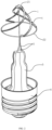
- Figs. 1-3 schematically shows the structure of a bulb having a filament structure according to the first embodiment of the present invention.
- the filament structure includes at least three filament substrates 1.
- the at least three filament substrates 1 each include a first end and a second end. The first end and the second end are used for connecting with the lead wire so as to supply power to the LED light-emitting element on the filament substrate 1.
- Each of the at least three filament substrates 1 extends in the manner of winding around an axis.
- the angle at which the section of the filament substrate that is between the first end and the second end wound around the axis is not exceed 720 degrees.
- the axes which the at least three filament substrates 1 are wound around coincide with each other.That is, the at least three filament substrates 1 are all wound around the same axis.
- the axes which the at least three filament substrates 1 are wound around are arranged parallel to each other or at a certain angle.
- the filament substrate 1 extends in a smooth curve around the axis between the first end and the second end, or extends in a fold line between the respective first end and second end.
- the first end and the second end of the at least three filament substrates 1 are spaced apart from each other, so that the at least three filament substrates exhibit a spatial distribution.
- the at least three filament substrates each extend in a spiral smooth curve between the first end and the second end.
- the first ends of the at least three filament substrates 1 are located in a first plane, and the second ends are located in a second plane. That is, the first ends of the at least three filament substrates 1 are all located in the same plane, and the second ends are all located on another same plane.
- the first plane and the second plane are separated from each other.
- the first plane and the second plane are parallel to each other, or may also be at a certain angle to each other.
- At least one of the first and second end of the at least three filament substrates 1 are connected to each other. That is, the first ends are connected together or the second ends are connected together. Alternatively, the first ends are connected together while the second ends are connected together.
- the first plane and the second plane are respectively provided with connectors, which are respectively connected to the ends of the filament substrate 1, namely the first end and the second end.
- the first plane is provided with a first connector 21, and the second plane is provided with a second connector 22.
- the first connector 21 connects the first ends of at least three filament substrates 1
- the second connector 22 connects the second ends of at least three filament substrates 1. Therefore, when the first connector 21 and the second connector 22 are respectively connected to the positive and negative leads 3, the at least three filament substrates 1 can be connected in parallel. It should be noted that, it is also possible that only one of the first connector 21 and the second connector 22 exist.
- the axes which the at least three filament substrates 1 are wound around coincide with each other. That is, the at least three filament substrates 1 are wound around the same axis.
- connection manner can also be used.
- the first connector 21 or the second connector 22 can be configured to form a disconnection, so that the first connector 21 or the second connector 22 respectively forms two portions disconnected with each other.
- Each portion is connected to at least one filament substrate 1, and each portion is connected to different leads, so that the at least three substrates 1 can be connected in series or in parallel with each other.
- the user can arrange the at least three filament substrates 1 as needed in different manners of connection.
- the at least three filament substrates 1 can be provided with multiple LED light-emitting elements.
- the multiple LED light-emitting elements can be connected in parallel or in series with each other.
- the material of the filament substrate 1 includes but is not limited to metal, organic glass, PVC,plastic, sapphire, ceramic and silica gel.
- the filament substrate 1 may be formed from one of the materials as described above, or may be fabricated by splicing and/or embedding from multiple materials in the materials as described above.
- the filament substrate 1 may also be PCB or FPCB, etc..
- the LED light-emitting element can be an LED chip, or an LED lamp bead or other packaged LED light-emitting unit.
- the LED chip can be a vertical chip, a horizontal chip, a white light chip or a flip chip. Furthermore, the LED light-emitting element of the filament substrate 1 can be fixed on the filament substrate 1 with transparent glue, conductive glue (such as silica gel, modified resin, epoxy resin, silver glue or copper glue), and then the LED light-emitting elements can be connected in series or in parallel through the chip connecting wires arranged on the filament substrate 1 or the wires preformed on the filament substrate 1.
- the outside of the LED light-emitting element may also be coated with a transparent medium layer serving for protection or light emitting.
- the material of the transparent medium layer is one of silica gel, epoxy resin and LED light-emitting powder glue, or the combination of some of them.
- Each of the at least three filament substrates 1 includes at least one substrate stripe.
- Each substrate stripe may extend along the same curved line or fold line, or wavy line, or irregular line, such as the irregular line including partial fold line and partial curved line.
- the at least one substrate stripe can extend long a spiral curve as shown in Figs. 1-3 , or other curved line, such as a regular or irregular wavy line, a circular arc line, or a fold line (such as a fold line folded back and forth, or a fold line folded sequentially in one direction).
- the at least one substrate stripe are spaced apart from each other in a three-dimensional space.
- each filament substrate has at least two substrates stripes
- the at least two substrates stripes are connected to each other, which may be partially overlapped or not overlapped, or connected at one end or connected at both ends, so that after the three-dimensional filament structure is formed, more spatial distribution shapes can be formed.
- the filament structure can present a variety of different styles spatially and can be spatially distributed more evenly, thereby making the illumination of the filament structure more uniform, omni-directional and multi-angle.
- the multiple substrate stripes in each filament substrate can extend and wind around the same axis.
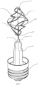
- the filament structure includes three filament substrates 1.
- Each of the three filament substrates 1 includes two substrate stripes. The first ends of the three filament substrates 1 are connected to the first connector 21. The second ends of the filament substrate 1 are separated from each other.
- the at least three filament substrates each includes at least one substrate stripes, and the width of the at least one substrate stripes gradually increases or decreases from the first end to the second end. Preferably, the width is gradually increased as the substrate stripe extends.
- This arrangement makes it more convenient and the overall structure stronger when the at least three filament substrates 1 are stretched from a plane into a three-dimensional structure.
- the filament substrate can be under a balanced force in the radial direction, so that the filament substrate is stretched under an uniform tensile force.
- Figs. 1 and 2 schematically shows a bulb with the filament structure.
- the bulb includes a lamp holder 4 and a lamp post 5 arranged on the lamp holder 4.
- the lamp post 5 is connected to the positive and negative leads 3, and the positive and negative leads 3 are respectively connected to the first and second ends of the at least three filament substrates.
- the positive and negative leads 3, the lamp post 5 and the at least three filament substrates 1 are housed ina light-transmitting lamp body 6, and the bottom of the light-transmitting lamp body 6 is fixedly connected to the lamp holder 4.
- the first connector 21 and the second connector 22 are parallel to each other, and the first connector 21 is located above the second connector 22.
- the at least three filament substrates 1 include four filament substrates 1.
- each filament substrate is connected to the first connector 21, and the second end of each filament substrate is connected to the second connector 22.
- the positive and negative leads 3 are respectively connected to the first connector 21 and the second connector 22.
- the lamp holder 4 is provided with an electric connector and a driver for connecting with an external power source and supplying power to the filament structure through the lamp post and the positive and negative leads.
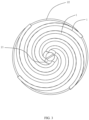
- FIG. 3 schematically shows the at least three filament substrates of this embodiment before processing.
- the first connector 21, the second connector 22, and the at least three filament substrates 1 are all located in the same plane.
- the first connector 21 and the second connector 22 are both ring-shaped members.
- the first connector 21 is arranged on the inner side of the second connector 22 in the radial direction and spaced apart from the second connector 22.
- the at least three filament substrates 1 are arranged between the first connector 21 and the second connector 22. That is, the at least three filament substrates 1 are all located in the same plane, and the first ends of the at least three filament substrates 1 are located on the inner side of the second ends in the radial direction.
- the at least three filament substrates 1 extends between the first end and the second end.
- the at least three filament substrates 1 extend spirally around the first connector 21 with intervals therebetween. That is, the at least three filament substrates 1 all extend and wind around a point, and the at least three filament substrates 1 all wind around the same point, namely, the center of the first connector 21. Therefore, to fabricate the filament structure, it only needs the processing performed in the same plane. For example, LED light-emitting elements, electrical connecting wires, and other packaging materials are applied on at least three filament substrates 1. After the processing, the filament structure with a three-dimensional structure can be stretched and formed at one time by simply stretching the first connector 21 and the second connector 22 apart from each other, without any unnecessary shaping and processing procedure.
- the filament structure with athree-dimensional structure can be formed by simply stretching the first connector 21 and the second connector 22 apart into different planes.
- the first connector 21 and the second connector 22 may also be components of other different structures, such as other solid structures like circular, square, etc., or other ring structures like elliptical ring, square ring, etc., or an arc-shaped structure.
- the first connector 21 and the second connector 22 are coaxially arranged and both have a ring structure.
- the first plane and the second plane are parallel to each other after performing the stretching process.
- the position where the first ends of the four filament substrates 1 are connected to the first connector 21 are evenly distributed along the circumferential direction of the first connector 21, that is, the four filament substrates 1 are evenly distributed in the three-dimensional space.
- the position where the second ends of the four filament substrates 1 are connected to the second connector 22 are evenly distributed along the circumferential direction of the second connector 22.
- the four filament substrates 1 are distributed spirally around the first connector 21 between the first connector 21 and the second connector 22.
- the four filament substrates 1 are arranged adjacently one after another.
- the first ends of the four filament substrates 1 are connected to the first connector 21, and the second ends of the four filament substrates 1 are separated from each other. That is, the second connector 22 can be omitted, so that during the processing, the four filament substrates 1 and the first connector 21 can be processed as a whole, following with the step of integrally packaging and then the step of stretching.
- the whole three-dimensional shape can be formed at one time by simply pulling the first connector 21 out of the plane.
- the filament structure does not necessarily adopt the above-mentioned manufacturing method.
- the filament structure can be configured such that the first connector 21 and the second connector 22 have the same ring structure and they may also be located respectively in different planes originally. Then, the filament substrates are connected to the first connector 21 and the second connector 22 respectively.
- the first connector 21 is placed on the inside of the second connector 22 in radial direction and is to be stretched.
- the processed three-dimensional filament structure is a three-dimensional filament structure with a smaller radial size at one end and a larger radial size at the other end.
- the at least three filament substrates 1 all wind around an axis, and the angle at which the second end winds and extends relative to the first end does not exceed 720 degrees.
- the at least three filament substrates 1 winds around the axis no more than two turns.
- the angle at which the section between the second end and the first end winds around the axis is about 270 degrees.
- the angle which the second end runs relative to the first end is greater than or equal to 90 degrees and less than or equal to 360 degrees.
- the first end is located on the inside of the second end in the radial direction.
- the filament structure extends in a curved line or fold line between the first plane and the second plane, which can form a three-dimensional filament distribution structure, resulting uniform, multiple-angle andomni-directional light emitting.
- the filament has a small structure and is distributed spatially.
- the LED light-emitting elements arranged on the filament substrate can facilitate heat dissipation, enabling both multi-angle and omni-directional illumination and heat dissipation.
- the filament structure can be easily processed and produced, and has an attractive appearance which may be a good decoration and have a great practicability.
- Figs. 4 and 5 schematically shows the bulb of the second embodiment of the invention. Similar to the first embodiment, the bulb includes a lamp holder 4, a lamp post 5 arranged on the lamp holder 4 and connected with positive and negative leads 3, and at least one filament structure which are connected to the positive and negative leads 3.
- the positive and negative leads 3, the lamp post 5 and the filament substrates are housed in a light-transmitting lamp body 6, and the bottom of the light-transmitting lamp body 6 is fixedly connected to the lamp holder 4.
- the bulb includes at least one filament structure, and the connector in the filament structure is connected with the positive and negative leads 3.
- Figs. 4 and 5 shows two filament structures. Each filament structure is the same as in the first embodiment. In the two filament structures, one of the first connector and the second connector is integrated.
- the second ends of the two filament structures are connected together, namely, the second connectors 22 of the two filament structures coincide with each other, or the two filament structures have a common second connectors 22.
- the two filament structures in the bulb forms a combination of two spiral structures that gradually increases in radial direction and then gradually decreases in radial direction.
- the positions where the second end of each filament substrate in the upper filament structure is connected to the second connector 22 respectively correspond to the positions where the second end of each filament substrate in the lower filament structure is connected to the second connector 22. That is, the second ends of the at least three filament substrates 1 in the upper filament structure and the second ends of the at least three filament substrates 1 in the lower filament structure are connected to each other.
- the upper filament structure is the same as the lower filament structure. Certainly, those skilled in the art can also understand that the structure of the upper and lower filament structures may also be different.
- first ends of the at least three filament substrates in the two filament structures are connected to each other. That is, the first connectors coincide with each other or the two filament structures have a common first connector 21.
- at least one of the first ends and the second ends of the at least three filament substrates in the two filament structures are located in the same plane.
- the connection between the filament structures may have a partial overlap or complete overlap, or the connection therebetween may be formed adjacently.
- both the first ends and the second ends are respectively located in the same plane with at least partial overlap or adjacent connection. That is, a plurality of filament structures arranged side by side are formed. The user can arbitrarily set the filament structure as required. Only two structures are exemplified above, and those skilled in the art can set this conversion according to different requirements.
- Fig. 6 schematically shows the bulb of the third embodiment of the present disclosure.
- the structure of the bulb is generally the same as that of the first and second embodiments, except for the filament structure.
- the bulb includes two filament structures.
- Each filament structure includes three filament substrates 1.
- Each filament substrate 1 includes a first end and a second end.
- Each filament substrate 1 includes a substrate strip.
- the substrate strip extends along a fold line, each substrate extends and winds around the axis.
- the section between the first end and the second end of the substrate winds around the axis for less than 90 degrees.
- the first ends of the three filament substrates 1 are all connected to the first connector 21, and the second ends of the three filament substrates are all connected to the second connector 22.
- the two filament structures have a common second connector 22.
- the first connectors 21 are arranged up and down separately, thus forming two filament structures that are inverted from each other.
- One of the positive and negative leads 3 of the bulb is respectively connected to the two first connectors 21 of the two filament structures, and the other one is connected to the common second connector 22 of the two filament structures.
- the substrate is in the shape of a fold line, and no LED light emitting element is provided in the bending area of the fold line.
- Fig. 7 schematically shows the fourth embodiment of the present invention.
- the bulb includes a lamp holder 4 and a lamp post 5 arranged on the lamp holder 4.
- the lamp post 5 is connected to the positive and negative leads 3, and the positive and negative leads 3 are respectively connected to the first and second ends of the at least three filament substrates.
- the positive and negative leads 3, the lamp post 5 and the at least three filament substrates 1 are housed in a light-transmitting lamp body 6, and the bottom of the light-transmitting lamp body 6 is fixedly connected to the lamp holder 4.
- this embodiment includes two above-mentioned filament structures, and the above-mentioned two filament structures are arranged horizontally.
- the two filament structures have only the first connector and do not have the second connector.
- Each of the two filament structures includes three uniformly distributed filament substrates 1. The second ends of the filament substrates 1 in the two filament structures are connected to each other. The first ends of the filament substrates 1 are all connected to the first connectors 21. The first connectors 21 of the two filament structures are respectively connected to the positive and negative electrodes in the positive and negative leads 3.
- various electrical connection methods are described in the above embodiments. It may be that only one of the first connector and the second connector is provided, or both the first connector and the second connector are provided.
- the first connector and the second connector are respectively connected to one of the positive and negative leads. That is, the first end and the second end are respectively connected to the positive and negative electrodes.
- the first ends and/or second ends of adjacent filament structures may be connected to each other.
- the second ends of the two filament structures are connected to each other, and the first ends of the two filament structures are connected to the positive and negative electrodes respectively. Therefore, those skilled in the art can set a variety of different electrical connection methods as needed, such as in parallel, in series, or in disconnection, etc.
- the control of the light-emitting elements on the filament is more convenient, achieving diversified control.
- each filament substrate since each filament substrate winds around the axis, each filament substrate can achieve 360-degree multi-angle and multi-directional illumination. Therefore, multiple filament substrates with different color temperatures can be set as needed, or a variety of filament substrates with different luminous effect can be set as needed, such as blinking, continuous, gradual changing, etc., so as to achieve diversified and intelligent lighting.
- the filament structure described above and the bulb having the filament structure are convenient to process and install, achieve multi-angle omni-directional illumination, and meet the requirements of heat dissipation.
- the filament structure has an attractive appearance that is easily used for decoration.
- the structure also enables multiple light-emitting elements at a filament to form multiple structures connected in parallel or in series, separate or simultaneous control of the light-emitting elements, and realizes arrangement of light-emitting elements of multiple colors, thereby achieving multiple lighting effects.
Description
- The present disclosure relates to an LED lighting device, in particular to an LED filament structure and a bulb having the same.
- As an emerging light source, LED has been widely used in the household and commercial lighting, and has gradually become a commonly used light source in daily life. However, the LED light source has the characteristics of high directivity and high heat generation. Therefore, it is difficult to apply to the small-sized bulb. In order to obtain omni-directional light emission, more LED light-emitting elements must be installed, which in turn requires a larger volume for heat dissipation. Therefore, the existing LED light source has either larger volume or lower brightness due to the limitation of its heat generation and volume restrictions.
- In the prior art, there are different types of LED package, including Lamp type, Chip On Boardtype, Surface Mount Device type, System In Package type, etc. According to different types of LED package, different package substrates are used.
- In general, the substrate for the Chip-On-Board LED package is a circuit board or a substrate made of a single material, such as metal, PVC, organic glass, plastic, etc., and the shape of the substrate is generally flat rectangle, flat circle or flat strip, etc. Furthermore, the edges of these substrates are usually smooth straight lines or curves.
- After setting the LED chip on the substrate and applying the fluorescent glue, the lightis emitted is a plane light. Even if a three-dimensional luminous body is formed by one or more substrates, the luminous body is likely to have uneven lighting angles distribution as the overall structure is hard to be designed perfectly. In addition, although the substrate can emit light in 360 degrees when it is made from light-transmitting material, the heat dissipation problems are usually caused. On the contrary, when the substrate is made of an opaque material, such as metal, there is no light emitting from the side where the LED chip is not provided, resulting in the inability to emit light in 360 degrees.
- In conclusion, the current Chip-On-Board LED package has an uneven light-emitting angles distribution, which makes it impossible to emit lights in multi-angle or multi-level. Additionally, the heat dissipation problem usually occurs and thus the light efficiency may be affected. Therefore, there is an urgent need to develop a high-efficiency LED package substrate that is equipped with LED chips and sealed with fluorescent glue, has a balanced light-emitting angle, completely multi-angle, multi-level light, and is easy to install and process.
-
WO 2015/096280 A1 discloses a full light distribution type LED bulb lamp with twisted-line-shaped lamp filament configuration is composed of a sealed light-emitting bulb shell, a sealing part which seals an opening on the bottom of the sealed light-emitting bulb shell, a light-emitting module and a lamp cap connected to the bottom of the sealing part. The light-emitting module is composed of a core column and k strip-shaped LED omni-directional lamp filaments, and the core column is vertically mounted above the sealing part. The strip-shaped LED omni-directional lamp filaments are arranged around the core column. The lamp further comprises a first supporting frame and a second supporting frame located above and below the core column. The connecting points of the strip-shaped LED omni-directional lamp filaments and the supporting frames are respectively located on a first projection circle and a second projection circle that have the same radius, have coinciding projections of circle centres in the vertical direction, and are located above and below the core column respectively. The lamp filament connecting points are evenly distributed on the respective projection circles at intervals. The included angles between two connecting points of each lamp filament and the connecting line of the circle centres of the respective projection circles are equal. -
WO 2015/185360 A1 discloses a filament structure according to the preamble ofclaim 1 of the present invention. - The invention is as set out in the set of claims.The technical problem to be solved by the present invention is to provide an LED filament structure and a bulb having the same, which is convenient for processing and installation, has good heat dissipation effect, and can provide uniform light emission in all directions and multiple angles.
- In order to solve the above-mentioned technical problems, the following technical solution is adopted: A filament structure comprising at least three filament substrates , characterized in that: each of the at least three filament substrates has a first end and a second end which are spaced apart from each other; sections between the first ends and the second ends of the at least three filament substrates extend and wind around an axis respectively; and an angle at which the sections of the at least three filament substrates between the first ends and the second ends are wound around the axis is not greater than 720 degrees.
- Each of the at least three filament substrates includes at least one substrate stripe, and the at least one substrate stripe extends between the first end and the second end in a fold line, a curved line, a wavy line, or an irregular line.
- In order to make the stretch easier to operate and avoid the filament substrate from being broken during pulling, the width of the at least one substrate stripe increases gradually or decreases gradually between the first end and the second end.
- Preferably, the first ends of the at least three filament substrates are located in a first plane, the second ends of the at least three filament substrates are located in a second plane, and the first plane and the second plane are parallel or not parallel to each other.
- Preferably, at least one of the first ends and the second ends of the at least three filament substrates are connected to a connector, or at least one of the first ends and the second ends of the at least three filament substrates are connected to each other.
- Preferably, the first ends and the second ends of the at least three filament substrates are respectively connected to a first connector provided in the first plane and a second connector provided in the second plane; and the first ends of the at least three filament substrates are all connected to the first connector and the second ends of the at least three filament substrates are all connected to the second connector.
- Preferably, the first connector and the second connector are arranged coaxially and/or in parallel.
- In order to facilitate processing and one-time stretching, the positions where the first ends of the at least three filament substrates are connected to the first connector are evenly or unevenly distributed along the circumferential direction of the first connector; and the positions where the second ends of the at least three filament substrates are connected to the second connector are evenly or unevenly distributed along the circumferential direction of the second connector.
- Preferably, the sections between the first ends and the second ends of the at least three filament substrates extend in a spiral smooth curve.
- Preferably, the axis around which the sections between the first ends and the second ends of each of the at least three filament substrates extend and wind are parallel to each other, coincided, or at a certain angle.
- Preferably, the at least three filament substrates are provided with a plurality of LED light-emitting elements, and the outside of the filament substrate and the LED light-emitting elements are covered with a medium layer serving for protection orlight emitting.
- A bulb comprising the above filament structure. The bulbcomprises a lamp holder and a lamp post arranged on the lamp holder, the lamp post being connected to a positive and negative lead, and the bulb comprising at least one filament structure, characterized in that: the positive and negative lead is connected to at least one filament structure; and a light-transmitting lamp body is provided to house the lamp post and at least three filament substrates.
- Preferably, the bulb comprises at least two filament structures. The first ends and/or the second ends of at least three filament substrates in the at least two filament structures are connected to each other.
- Preferably, the first ends of at least three filament substrates in the two filament structures are connected to the first connector respectively; the second ends of at least three filament substrates in the two filament structures are connected to a second connector respectively; and the first connectors and/or the second connectors of the two filament structures are at least partially overlapped and connected.
- Compared with the prior art, the advantage of the present invention lies in that: The filament structure and the bulb having the filament structure are convenient to process and install, achieve multi-angle omni-directional illumination, and meet the requirements of heat dissipation. The filament structure has an attractive appearance that is easily used for decoration. The structure also enables multiple light-emitting elements at a filament to form multiple structures connected in parallel or in series, separate or simultaneous control of the light-emitting elements, and realizes arrangement of light-emitting elements of multiple colors, thereby achieving multiple lighting effects.
-
-
Fig. 1 schematically shows a three-dimensional structure of the bulb according to the first embodiment of the present invention; -
Fig. 2 schematically shows the filament structure according to the first embodiment of the present invention; -
Fig. 3 schematically shows the plan view of the filament structure according to the first embodiment of the present invention before being stretched; -
Fig. 4 schematically shows a three-dimensional structure of the bulb according to a second embodiment of the present invention; -
Fig. 5 schematically shows a structure of the bulb according to the second embodiment of the present invention; -
Fig. 6 schematically shows a structure of the bulb according to the third embodiment of the present invention; -
Fig. 7 schematically shows a structure of the bulb according to the fourth embodiment of the present invention; and -
Fig. 8 shows another alternative embodiment of the filament structure of the present invention. - The invention will be described in further detail with reference to the accompanying drawings.
-
Figs. 1-3 schematically shows the structure of a bulb having a filament structure according to the first embodiment of the present invention. As shown inFigs. 1 and2 , the filament structure includes at least threefilament substrates 1. The at least threefilament substrates 1 each include a first end and a second end. The first end and the second end are used for connecting with the lead wire so as to supply power to the LED light-emitting element on thefilament substrate 1. - Each of the at least three
filament substrates 1 extends in the manner of winding around an axis. The angle at which the section of the filament substrate that is between the first end and the second end wound around the axis is not exceed 720 degrees. Preferably, the axes which the at least threefilament substrates 1 are wound around coincide with each other.That is, the at least threefilament substrates 1 are all wound around the same axis. Alternatively, the axes which the at least threefilament substrates 1 are wound around are arranged parallel to each other or at a certain angle. Thefilament substrate 1 extends in a smooth curve around the axis between the first end and the second end, or extends in a fold line between the respective first end and second end. - The first end and the second end of the at least three
filament substrates 1 are spaced apart from each other, so that the at least three filament substrates exhibit a spatial distribution. As shown inFigs. 1-3 , preferably, the at least three filament substrates each extend in a spiral smooth curve between the first end and the second end. Preferably, the first ends of the at least threefilament substrates 1 are located in a first plane, and the second ends are located in a second plane. That is, the first ends of the at least threefilament substrates 1 are all located in the same plane, and the second ends are all located on another same plane. The first plane and the second plane are separated from each other. The first plane and the second plane are parallel to each other, or may also be at a certain angle to each other. - In addition, at least one of the first and second end of the at least three
filament substrates 1 are connected to each other. That is, the first ends are connected together or the second ends are connected together. Alternatively, the first ends are connected together while the second ends are connected together. - As shown in
Figs. 1-3 , the first plane and the second plane are respectively provided with connectors, which are respectively connected to the ends of thefilament substrate 1, namely the first end and the second end. The first plane is provided with afirst connector 21, and the second plane is provided with asecond connector 22. Thefirst connector 21 connects the first ends of at least threefilament substrates 1, and thesecond connector 22 connects the second ends of at least threefilament substrates 1. Therefore, when thefirst connector 21 and thesecond connector 22 are respectively connected to the positive andnegative leads 3, the at least threefilament substrates 1 can be connected in parallel. It should be noted that, it is also possible that only one of thefirst connector 21 and thesecond connector 22 exist. That is, only the first or second ends of the at least threefilament substrates 1 are connected to the connector, while the other one of the first or second ends may be separated freely. And in this embodiment, the axes which the at least threefilament substrates 1 are wound around coincide with each other. That is, the at least threefilament substrates 1 are wound around the same axis. - It should be noted that, other connection manner can also be used. For example, the
first connector 21 or thesecond connector 22 can be configured to form a disconnection, so that thefirst connector 21 or thesecond connector 22 respectively forms two portions disconnected with each other. Each portion is connected to at least onefilament substrate 1, and each portion is connected to different leads, so that the at least threesubstrates 1 can be connected in series or in parallel with each other. The user can arrange the at least threefilament substrates 1 as needed in different manners of connection. - The at least three
filament substrates 1 can be provided with multiple LED light-emitting elements. The multiple LED light-emitting elements can be connected in parallel or in series with each other. The material of thefilament substrate 1 includes but is not limited to metal, organic glass, PVC,plastic, sapphire, ceramic and silica gel. Thefilament substrate 1 may be formed from one of the materials as described above, or may be fabricated by splicing and/or embedding from multiple materials in the materials as described above. Thefilament substrate 1 may also be PCB or FPCB, etc.. The LED light-emitting element can be an LED chip, or an LED lamp bead or other packaged LED light-emitting unit. The LED chip can be a vertical chip, a horizontal chip, a white light chip or a flip chip. Furthermore, the LED light-emitting element of thefilament substrate 1 can be fixed on thefilament substrate 1 with transparent glue, conductive glue (such as silica gel, modified resin, epoxy resin, silver glue or copper glue), and then the LED light-emitting elements can be connected in series or in parallel through the chip connecting wires arranged on thefilament substrate 1 or the wires preformed on thefilament substrate 1. The outside of the LED light-emitting element may also be coated with a transparent medium layer serving for protection or light emitting. The material of the transparent medium layer is one of silica gel, epoxy resin and LED light-emitting powder glue, or the combination of some of them. - Each of the at least three
filament substrates 1 includes at least one substrate stripe. Each substrate stripe may extend along the same curved line or fold line, or wavy line, or irregular line, such as the irregular line including partial fold line and partial curved line. The at least one substrate stripe can extend long a spiral curve as shown inFigs. 1-3 , or other curved line, such as a regular or irregular wavy line, a circular arc line, or a fold line (such as a fold line folded back and forth, or a fold line folded sequentially in one direction). The at least one substrate stripe are spaced apart from each other in a three-dimensional space. When each filament substrate has at least two substrates stripes, the at least two substrates stripes are connected to each other, which may be partially overlapped or not overlapped, or connected at one end or connected at both ends, so that after the three-dimensional filament structure is formed, more spatial distribution shapes can be formed. In this way, the filament structure can present a variety of different styles spatially and can be spatially distributed more evenly, thereby making the illumination of the filament structure more uniform, omni-directional and multi-angle. The more substrates stripes the filament substrate includes, the more uniform and omni-directionalthe spatial distribution of light-emitting points is, after forming the three-dimensional structure. The multiple substrate stripes in each filament substrate can extend and wind around the same axis. As shown inFigure 8 , the filament structure includes threefilament substrates 1. Each of the threefilament substrates 1 includes two substrate stripes. The first ends of the threefilament substrates 1 are connected to thefirst connector 21. The second ends of thefilament substrate 1 are separated from each other. - According to the invention, the at least three filament substrates each includes at least one substrate stripes, and the width of the at least one substrate stripes gradually increases or decreases from the first end to the second end. Preferably, the width is gradually increased as the substrate stripe extends. This arrangement makes it more convenient and the overall structure stronger when the at least three
filament substrates 1 are stretched from a plane into a three-dimensional structure. In addition, during the stretching process, the filament substrate can be under a balanced force in the radial direction, so that the filament substrate is stretched under an uniform tensile force. -
Figs. 1 and2 schematically shows a bulb with the filament structure. The bulb includes alamp holder 4 and alamp post 5 arranged on thelamp holder 4. Thelamp post 5 is connected to the positive andnegative leads 3, and the positive andnegative leads 3 are respectively connected to the first and second ends of the at least three filament substrates. The positive andnegative leads 3, thelamp post 5 and the at least threefilament substrates 1 are housed ina light-transmittinglamp body 6, and the bottom of the light-transmittinglamp body 6 is fixedly connected to thelamp holder 4. As shown inFigs. 1 and2 , thefirst connector 21 and thesecond connector 22 are parallel to each other, and thefirst connector 21 is located above thesecond connector 22. The at least threefilament substrates 1 include fourfilament substrates 1. The first end of each filament substrate is connected to thefirst connector 21, and the second end of each filament substrate is connected to thesecond connector 22. The positive andnegative leads 3 are respectively connected to thefirst connector 21 and thesecond connector 22. The section of the at least threefilament substrates 1 that extends spirally between the first end and the second end. Thelamp holder 4 is provided with an electric connector and a driver for connecting with an external power source and supplying power to the filament structure through the lamp post and the positive and negative leads. -
FIG. 3 schematically shows the at least three filament substrates of this embodiment before processing. As shown inFIG. 3 , thefirst connector 21, thesecond connector 22, and the at least threefilament substrates 1 are all located in the same plane. Thefirst connector 21 and thesecond connector 22 are both ring-shaped members. Thefirst connector 21 is arranged on the inner side of thesecond connector 22 in the radial direction and spaced apart from thesecond connector 22. The at least threefilament substrates 1 are arranged between thefirst connector 21 and thesecond connector 22. That is, the at least threefilament substrates 1 are all located in the same plane, and the first ends of the at least threefilament substrates 1 are located on the inner side of the second ends in the radial direction. The at least threefilament substrates 1 extends between the first end and the second end. Preferably, the at least threefilament substrates 1 extend spirally around thefirst connector 21 with intervals therebetween. That is, the at least threefilament substrates 1 all extend and wind around a point, and the at least threefilament substrates 1 all wind around the same point, namely, the center of thefirst connector 21. Therefore, to fabricate the filament structure, it only needs the processing performed in the same plane. For example, LED light-emitting elements, electrical connecting wires, and other packaging materials are applied on at least threefilament substrates 1. After the processing, the filament structure with a three-dimensional structure can be stretched and formed at one time by simply stretching thefirst connector 21 and thesecond connector 22 apart from each other, without any unnecessary shaping and processing procedure. That is, the filament structure with athree-dimensional structure can be formed by simply stretching thefirst connector 21 and thesecond connector 22 apart into different planes. And those skilled in the art can also understand that thefirst connector 21 and thesecond connector 22 may also be components of other different structures, such as other solid structures like circular, square, etc., or other ring structures like elliptical ring, square ring, etc., or an arc-shaped structure. - Preferably, in this embodiment, the
first connector 21 and thesecond connector 22 are coaxially arranged and both have a ring structure. The first plane and the second plane are parallel to each other after performing the stretching process. The position where the first ends of the fourfilament substrates 1 are connected to thefirst connector 21 are evenly distributed along the circumferential direction of thefirst connector 21, that is, the fourfilament substrates 1 are evenly distributed in the three-dimensional space. The position where the second ends of the fourfilament substrates 1 are connected to thesecond connector 22 are evenly distributed along the circumferential direction of thesecond connector 22. The fourfilament substrates 1 are distributed spirally around thefirst connector 21 between thefirst connector 21 and thesecond connector 22. The fourfilament substrates 1 are arranged adjacently one after another. - Preferably, the first ends of the four
filament substrates 1 are connected to thefirst connector 21, and the second ends of the fourfilament substrates 1 are separated from each other. That is, thesecond connector 22 can be omitted, so that during the processing, the fourfilament substrates 1 and thefirst connector 21 can be processed as a whole, following with the step of integrally packaging and then the step of stretching. The whole three-dimensional shape can be formed at one time by simply pulling thefirst connector 21 out of the plane. - It should be noted that, the filament structure does not necessarily adopt the above-mentioned manufacturing method. For example, the filament structure can be configured such that the
first connector 21 and thesecond connector 22 have the same ring structure and they may also be located respectively in different planes originally. Then, the filament substrates are connected to thefirst connector 21 and thesecond connector 22 respectively. In the above method, thefirst connector 21 is placed on the inside of thesecond connector 22 in radial direction and is to be stretched. The processed three-dimensional filament structure is a three-dimensional filament structure with a smaller radial size at one end and a larger radial size at the other end. The at least threefilament substrates 1 all wind around an axis, and the angle at which the second end winds and extends relative to the first end does not exceed 720 degrees. That is, the at least threefilament substrates 1 winds around the axis no more than two turns. As shown inFigs. 1-3 . the angle at which the section between the second end and the first end winds around the axis is about 270 degrees. In this way, more substrates is allowed to be set in a certain area during processing, and it may facilitate the convenience and efficient as well as structure stability when the filament is stretched out of a flat structure into a three dimensional structure. Preferably, the angle which the second end runs relative to the first end is greater than or equal to 90 degrees and less than or equal to 360 degrees. Preferably, when the at least three filament substrates are located in a plane and have not been stretched, the first end is located on the inside of the second end in the radial direction. - With such a filament structure, it is convenient to process. Additionally, the filament structure extends in a curved line or fold line between the first plane and the second plane, which can form a three-dimensional filament distribution structure, resulting uniform, multiple-angle andomni-directional light emitting. Moreover, the filament has a small structure and is distributed spatially. The LED light-emitting elements arranged on the filament substrate can facilitate heat dissipation, enabling both multi-angle and omni-directional illumination and heat dissipation. In addition, the filament structure can be easily processed and produced, and has an attractive appearance which may be a good decoration and have a great practicability.
- Moreover, in the above-mentioned embodiment, since multiple filament substrates are provided, different LED light-emitting elements can be provided on each filament substrate and may be controlled individually. Therefore, individual control and layout may be performed with regard to multiple colors and multiple types of lamps, realizing a variety of lighting effects and lighting control.
-
Figs. 4 and5 schematically shows the bulb of the second embodiment of the invention. Similar to the first embodiment, the bulb includes alamp holder 4, alamp post 5 arranged on thelamp holder 4 and connected with positive andnegative leads 3, and at least one filament structure which are connected to the positive andnegative leads 3. The positive andnegative leads 3, thelamp post 5 and the filament substrates are housed in a light-transmittinglamp body 6, and the bottom of the light-transmittinglamp body 6 is fixedly connected to thelamp holder 4. The bulb includes at least one filament structure, and the connector in the filament structure is connected with the positive andnegative leads 3.Figs. 4 and5 shows two filament structures. Each filament structure is the same as in the first embodiment. In the two filament structures, one of the first connector and the second connector is integrated. That is, the second ends of the two filament structures are connected together, namely, thesecond connectors 22 of the two filament structures coincide with each other, or the two filament structures have a commonsecond connectors 22. The two filament structures in the bulb forms a combination of two spiral structures that gradually increases in radial direction and then gradually decreases in radial direction. In this embodiment, there is only one commonsecond connector 22. The positions where the second end of each filament substrate in the upper filament structure is connected to thesecond connector 22 respectively correspond to the positions where the second end of each filament substrate in the lower filament structure is connected to thesecond connector 22. That is, the second ends of the at least threefilament substrates 1 in the upper filament structure and the second ends of the at least threefilament substrates 1 in the lower filament structure are connected to each other. The upper filament structure is the same as the lower filament structure. Certainly, those skilled in the art can also understand that the structure of the upper and lower filament structures may also be different. - It should be noted that, it may also be possible that the first ends of the at least three filament substrates in the two filament structures are connected to each other. That is, the first connectors coincide with each other or the two filament structures have a common
first connector 21. Thus, a combination of two spiral structures, which gradually decreases in radial direction and then gradually increases in radial direction, is formed. It can also be possible that at least one of the first ends and the second ends of the at least three filament substrates in the two filament structures are located in the same plane. The connection between the filament structures may have a partial overlap or complete overlap, or the connection therebetween may be formed adjacently. Alternatively, both the first ends and the second ends are respectively located in the same plane with at least partial overlap or adjacent connection. That is, a plurality of filament structures arranged side by side are formed. The user can arbitrarily set the filament structure as required. Only two structures are exemplified above, and those skilled in the art can set this conversion according to different requirements. -
Fig. 6 schematically shows the bulb of the third embodiment of the present disclosure. In this embodiment, the structure of the bulb is generally the same as that of the first and second embodiments, except for the filament structure. The bulb includes two filament structures. Each filament structure includes threefilament substrates 1. Eachfilament substrate 1 includes a first end and a second end. Eachfilament substrate 1 includes a substrate strip. The substrate strip extends along a fold line, each substrate extends and winds around the axis. The section between the first end and the second end of the substrate winds around the axis for less than 90 degrees. The first ends of the threefilament substrates 1 are all connected to thefirst connector 21, and the second ends of the three filament substrates are all connected to thesecond connector 22. The two filament structures have a commonsecond connector 22. Thefirst connectors 21 are arranged up and down separately, thus forming two filament structures that are inverted from each other. One of the positive andnegative leads 3 of the bulb is respectively connected to the twofirst connectors 21 of the two filament structures, and the other one is connected to the commonsecond connector 22 of the two filament structures. Moreover, in this embodiment, the substrate is in the shape of a fold line, and no LED light emitting element is provided in the bending area of the fold line. By such structure, the break and circuit failure is unlikely to occur after the filament substrates are stretched from a plane to a three-dimensional structure. Therefore, those skilled in the art can understand that the LED light-emitting elements can be arranged on the entire filament substrate uniformly, or arranged in partial areas, or in sub-regions. That is, the applied force during the filament stretching process can be guided to the area free of LED, so that the filament structure prevents damage to the LED light-emitting element due to twisting and bending during processing. -
Fig. 7 schematically shows the fourth embodiment of the present invention. Similarly to the bulbs in the first and second embodiments, the bulb includes alamp holder 4 and alamp post 5 arranged on thelamp holder 4. Thelamp post 5 is connected to the positive andnegative leads 3, and the positive andnegative leads 3 are respectively connected to the first and second ends of the at least three filament substrates. The positive andnegative leads 3, thelamp post 5 and the at least threefilament substrates 1 are housed in a light-transmittinglamp body 6, and the bottom of the light-transmittinglamp body 6 is fixedly connected to thelamp holder 4. The difference lies in that this embodiment includes two above-mentioned filament structures, and the above-mentioned two filament structures are arranged horizontally. The two filament structures have only the first connector and do not have the second connector. Each of the two filament structures includes three uniformly distributedfilament substrates 1. The second ends of thefilament substrates 1 in the two filament structures are connected to each other. The first ends of thefilament substrates 1 are all connected to thefirst connectors 21. Thefirst connectors 21 of the two filament structures are respectively connected to the positive and negative electrodes in the positive andnegative leads 3. - Therefore, it should be noted that various electrical connection methods are described in the above embodiments. It may be that only one of the first connector and the second connector is provided, or both the first connector and the second connector are provided. The first connector and the second connector are respectively connected to one of the positive and negative leads. That is, the first end and the second end are respectively connected to the positive and negative electrodes. Alternatively, when there are two or more filament structures, the first ends and/or second ends of adjacent filament structures may be connected to each other. As described in the fourth embodiment, the second ends of the two filament structures are connected to each other, and the first ends of the two filament structures are connected to the positive and negative electrodes respectively. Therefore, those skilled in the art can set a variety of different electrical connection methods as needed, such as in parallel, in series, or in disconnection, etc. Thus the control of the light-emitting elements on the filament is more convenient, achieving diversified control.
- Moreover, since each filament substrate winds around the axis, each filament substrate can achieve 360-degree multi-angle and multi-directional illumination. Therefore, multiple filament substrates with different color temperatures can be set as needed, or a variety of filament substrates with different luminous effect can be set as needed, such as blinking, continuous, gradual changing, etc., so as to achieve diversified and intelligent lighting.
- The filament structure described above and the bulb having the filament structure are convenient to process and install, achieve multi-angle omni-directional illumination, and meet the requirements of heat dissipation. The filament structure has an attractive appearance that is easily used for decoration. The structure also enables multiple light-emitting elements at a filament to form multiple structures connected in parallel or in series, separate or simultaneous control of the light-emitting elements, and realizes arrangement of light-emitting elements of multiple colors, thereby achieving multiple lighting effects.
Claims (12)
- A filament structure comprising at least three filament substrates (1), wherein:each of the at least three filament substrates (1) has a first end and a second end which are spaced apart from each other;sections between the first ends and the second ends of the at least three filament substrates (1) extend and wind around an axis respectively; andan angle at which the sections of the at least three filament substrates (1) between the first ends and the second ends are wound around the axis is not greater than 720 degrees wherein each of the at least three filament substrates (1) includes at least one substrate stripe; andthe at least one substrate stripe extends between the first end and the second end in a fold line, a curved line, a wavy line, or an irregular line,characterized in that: the width of the at least one substrate stripe increases gradually or decreases gradually between the first end and the second end.
- The filament structure according to claim 1, wherein:
the first ends of the at least three filament substrates (1) are located in a first plane, the second ends of the at least three filament substrates (1) are located in a second plane, and the first plane and the second plane are parallel or not parallel to each other. - The filament structure according to claim 1, wherein:
at least one of the first ends and the second ends of the at least three filament substrates (1) are connected to a connector, or at least one of the first ends and the second ends of the at least three filament substrates (1) are connected to each other. - The filament structure according to claim 2, wherein:the first ends and the second ends of the at least three filament substrates (1) are respectively connected to a first connector (21) provided in the first plane and a second connector (22) provided in the second plane; andthe first ends of the at least three filament substrates (1) are all connected to the first connector (21) and the second ends of the at least three filament substrates (1) are all connected to the second connector (22).
- The filament structure according to claim 4, wherein:
the first connector (21) and the second connector (22) are arranged coaxially and/or in parallel. - The filament structure according to claim 5, wherein:the positions where the first ends of the at least three filament substrates (1) are connected to the first connector (21) are evenly or unevenly distributed along the circumferential direction of the first connector (21); andthe positions where the second ends of the at least three filament substrates (1) are connected to the second connector (22) are evenly or unevenly distributed along the circumferential direction of the second connector (22).
- The filament structure according to any one of claims 1-6, wherein:
the sections between the first ends and the second ends of the at least three filament substrates (1) extend in a spiral smooth curve. - The filament structure according to any one of claims 1-6, wherein: the axis around which the sections between the first ends and the second ends of each of the at least three filament substrates (1) extend and wind are parallel to each other, coincided, or at a certain angle.
- The filament structure according to claim 8, wherein:
the at least three filament substrates (1) are provided with a plurality of LED light-emitting elements, and the outside of the filament substrate and the LED light-emitting elements are covered with a medium layer serving for protection orlight emitting. - A bulb comprising the filament structure as claimed in any one of claims 1-9, comprising a lamp holder (4) and a lamp post (5) arranged on the lamp holder (4), the lamp post (5) being connected to a positive and negative lead (3), and the bulb comprising at least one filament structure, wherein:the positive and negative lead (3) is connected to at least one filament structure; anda light-transmitting lamp body (6) is provided to house the lamp post (5) and at least three filament substrates (1).
- The bulb according to claim 10, wherein:the bulb comprises at least two filament structures; andthe first ends and/or the second ends of at least three filament substrates (1) in the at least two filament structures are connected to each other.
- The bulb according to claim 11, wherein:the first ends of at least three filament substrates (1) in the two filament structures are connected to the first connector (21) respectively;the second ends of at least three filament substrates (1) in the two filament structures are connected to a second connector (22) respectively; andthe first connectors (21) and/or the second connectors (21) of the two filament structures are at least partially overlapped and connected.
Applications Claiming Priority (2)
| Application Number | Priority Date | Filing Date | Title |
|---|---|---|---|
| CN201810668630 | 2018-06-23 | ||
| PCT/CN2019/091647 WO2019242596A1 (en) | 2018-06-23 | 2019-06-18 | Filament structure and bulb having the filament structure |
Publications (3)
| Publication Number | Publication Date |
|---|---|
| EP3812647A1 EP3812647A1 (en) | 2021-04-28 |
| EP3812647A4 EP3812647A4 (en) | 2022-03-16 |
| EP3812647B1 true EP3812647B1 (en) | 2023-09-20 |
Family
ID=64074953
Family Applications (1)
| Application Number | Title | Priority Date | Filing Date |
|---|---|---|---|
| EP19823500.4A Active EP3812647B1 (en) | 2018-06-23 | 2019-06-18 | Filament structure and bulb having the filament structure |
Country Status (5)
| Country | Link |
|---|---|
| US (1) | US11221109B2 (en) |
| EP (1) | EP3812647B1 (en) |
| CN (2) | CN108799863A (en) |
| ES (1) | ES2964481T3 (en) |
| WO (1) | WO2019242596A1 (en) |
Families Citing this family (6)
| Publication number | Priority date | Publication date | Assignee | Title |
|---|---|---|---|---|
| CN106322159A (en) * | 2016-10-19 | 2017-01-11 | 漳州立达信光电子科技有限公司 | LED filament lamp |
| CN108799863A (en) * | 2018-06-23 | 2018-11-13 | 杭州思隽思科技有限公司 | A kind of filamentray structure and the light bulb with the filamentray structure |
| CN108826032B (en) * | 2018-07-23 | 2024-02-09 | 杭州思隽思科技有限公司 | Novel LED filament |
| PL3987218T3 (en) * | 2019-06-24 | 2023-05-02 | Signify Holding B.V. | Color temperature controllable lighting device comprising different led filaments |
| CN114502876A (en) * | 2019-10-01 | 2022-05-13 | 昕诺飞控股有限公司 | LED filament device |
| USD1018258S1 (en) * | 2020-08-06 | 2024-03-19 | Hangzhou Sijunsi Technology Co., Ltd | LED filament |
Family Cites Families (22)
| Publication number | Priority date | Publication date | Assignee | Title |
|---|---|---|---|---|
| JP5864349B2 (en) | 2012-04-20 | 2016-02-17 | スタンレー電気株式会社 | LED bulb |
| CN203500919U (en) * | 2013-10-15 | 2014-03-26 | 江苏华英光宝科技股份有限公司 | Power supply hidden type LED bulb |
| CN203656627U (en) * | 2013-12-02 | 2014-06-18 | 张晓峰 | Lamp bulb with one spiral LED lamp filament |
| WO2015081804A1 (en) * | 2013-12-02 | 2015-06-11 | 张晓峰 | Spiral led filament and light bulb using spiral led filament |
| CN103712105A (en) * | 2013-12-26 | 2014-04-09 | 四川柏狮光电技术有限公司 | Full light distribution type LED bulb lamp with twisted-line-shaped lamp filaments distributed |
| CN203797384U (en) * | 2013-12-26 | 2014-08-27 | 四川柏狮光电技术有限公司 | LED bulb lamp with rotary lamp filaments |
| CN203797394U (en) | 2014-01-23 | 2014-08-27 | 浙江星碧照明科技有限公司 | Lamp |
| CN106415116A (en) * | 2014-06-05 | 2017-02-15 | 飞利浦照明控股有限公司 | Lighting device, luminaire and manufacturing method |
| HK1207250A2 (en) * | 2014-10-15 | 2016-01-22 | 新照明設計有限公司 號 | Substrate for led package, a tridimensional led package having the substrate, a light bulb having the tridimensional led package and methods for producing the same led led led |
| CN204187337U (en) | 2014-11-04 | 2015-03-04 | 浙江锐迪生光电有限公司 | A kind of LED silk lamp with screw type LED silk |
| CN204345344U (en) * | 2014-12-31 | 2015-05-20 | 苏州紫昱天成光电有限公司 | LED silk and use the bulb of this LED silk |
| CN204756550U (en) * | 2015-07-07 | 2015-11-11 | 厦门登斯特照明科技有限公司 | Novel LED filament lighting bulb |
| CN205001912U (en) * | 2015-09-11 | 2016-01-27 | 葛铁汉 | Space multi -angle LED bulb that gives out light; give off light |
| US20190226643A1 (en) * | 2016-07-19 | 2019-07-25 | Katerra Inc. | Led filament |
| CN106678580A (en) * | 2016-12-28 | 2017-05-17 | 上海应用技术大学 | Manufacturing method for spiral LED lamp filament inside bulb lamp |
| US20180204984A1 (en) * | 2017-01-13 | 2018-07-19 | Intematix Corporation | Narrow-band red phosphors for led lamps |
| CN106870970A (en) * | 2017-03-02 | 2017-06-20 | 海宁市欧亚电器有限公司 | A kind of LED of double helix lamp bead |
| WO2018201643A1 (en) * | 2017-05-05 | 2018-11-08 | 广明源光科技股份有限公司 | Led lamp structure and preparation process therefor |
| CN107270148A (en) * | 2017-07-31 | 2017-10-20 | 漳州立达信光电子科技有限公司 | LED filament lamp |
| US10605447B2 (en) * | 2018-04-24 | 2020-03-31 | Xiamen Eco Lighting Co. Ltd. | LED filament bulb apparatus |
| CN108826041A (en) | 2018-06-23 | 2018-11-16 | 杭州思隽思科技有限公司 | A kind of manufacturing method of filamentray structure |
| CN108799863A (en) | 2018-06-23 | 2018-11-13 | 杭州思隽思科技有限公司 | A kind of filamentray structure and the light bulb with the filamentray structure |
-
2018
- 2018-07-05 CN CN201810730526.3A patent/CN108799863A/en active Pending
- 2018-07-05 CN CN201821063213.9U patent/CN208652172U/en active Active
-
2019
- 2019-06-18 ES ES19823500T patent/ES2964481T3/en active Active
- 2019-06-18 EP EP19823500.4A patent/EP3812647B1/en active Active
- 2019-06-18 WO PCT/CN2019/091647 patent/WO2019242596A1/en unknown
- 2019-06-18 US US17/051,289 patent/US11221109B2/en active Active
Also Published As
| Publication number | Publication date |
|---|---|
| EP3812647A1 (en) | 2021-04-28 |
| ES2964481T3 (en) | 2024-04-08 |
| WO2019242596A1 (en) | 2019-12-26 |
| CN108799863A (en) | 2018-11-13 |
| CN208652172U (en) | 2019-03-26 |
| EP3812647A4 (en) | 2022-03-16 |
| US20210199250A1 (en) | 2021-07-01 |
| US11221109B2 (en) | 2022-01-11 |
Similar Documents
| Publication | Publication Date | Title |
|---|---|---|
| EP3812647B1 (en) | Filament structure and bulb having the filament structure | |
| US10006596B2 (en) | Color changing light and related light chain thereof | |
| US10436392B2 (en) | LED filament light | |
| WO2016058539A1 (en) | Substrate used for led encapsulation, three-dimensional led encapsulation, bulb comprising three-dimensional led encapsulation and manufacturing method therefor | |
| WO2015081804A1 (en) | Spiral led filament and light bulb using spiral led filament | |
| CN102575818A (en) | Lamp | |
| JP3187458U (en) | Light emitting diode bulb | |
| US20200056748A1 (en) | Led bulb | |
| CN205001912U (en) | Space multi -angle LED bulb that gives out light; give off light | |
| US11346508B2 (en) | LED filament | |
| CN206422098U (en) | LED lamp filament with heat radiation structure and LED bulb using LED lamp filament | |
| CN205001884U (en) | Multi -level luminous LED bulb | |
| CN204227103U (en) | Lamp device and lighting device | |
| CN210662366U (en) | Wound filament and bulb with same | |
| EP3349261B1 (en) | Multilevel light emitting led substrate and package, and bulb | |
| CN208652174U (en) | A kind of New LED filament | |
| CN108826041A (en) | A kind of manufacturing method of filamentray structure | |
| US11940107B2 (en) | Lighting device and a method of manufacturing a lighting device | |
| CN210662367U (en) | Filament and bulb with same | |
| CN213150721U (en) | Flexible filament lamp | |
| EP4042063B1 (en) | A lighting device | |
| CN102374410B (en) | LED (light emitting diode) bulb device | |
| JP2024501704A (en) | led filament interconnect ring | |
| WO2007101384A1 (en) | A flexible neon light |
Legal Events
| Date | Code | Title | Description |
|---|---|---|---|
| STAA | Information on the status of an ep patent application or granted ep patent |
Free format text: STATUS: THE INTERNATIONAL PUBLICATION HAS BEEN MADE |
|
| STAA | Information on the status of an ep patent application or granted ep patent |
Free format text: STATUS: THE INTERNATIONAL PUBLICATION HAS BEEN MADE |
|
| PUAI | Public reference made under article 153(3) epc to a published international application that has entered the european phase |
Free format text: ORIGINAL CODE: 0009012 |
|
| STAA | Information on the status of an ep patent application or granted ep patent |
Free format text: STATUS: REQUEST FOR EXAMINATION WAS MADE |
|
| 17P | Request for examination filed |
Effective date: 20201116 |
|
| AK | Designated contracting states |
Kind code of ref document: A1 Designated state(s): AL AT BE BG CH CY CZ DE DK EE ES FI FR GB GR HR HU IE IS IT LI LT LU LV MC MK MT NL NO PL PT RO RS SE SI SK SM TR |
|
| AX | Request for extension of the european patent |
Extension state: BA ME |
|
| DAV | Request for validation of the european patent (deleted) | ||
| DAX | Request for extension of the european patent (deleted) | ||
| A4 | Supplementary search report drawn up and despatched |
Effective date: 20220214 |
|
| RIC1 | Information provided on ipc code assigned before grant |
Ipc: F21V 19/00 20060101ALI20220208BHEP Ipc: F21K 9/235 20160101ALI20220208BHEP Ipc: F21K 9/232 20160101AFI20220208BHEP |
|
| GRAP | Despatch of communication of intention to grant a patent |
Free format text: ORIGINAL CODE: EPIDOSNIGR1 |
|
| STAA | Information on the status of an ep patent application or granted ep patent |
Free format text: STATUS: GRANT OF PATENT IS INTENDED |
|
| INTG | Intention to grant announced |
Effective date: 20230419 |
|
| GRAS | Grant fee paid |
Free format text: ORIGINAL CODE: EPIDOSNIGR3 |
|
| GRAA | (expected) grant |
Free format text: ORIGINAL CODE: 0009210 |
|
| STAA | Information on the status of an ep patent application or granted ep patent |
Free format text: STATUS: THE PATENT HAS BEEN GRANTED |
|
| AK | Designated contracting states |
Kind code of ref document: B1 Designated state(s): AL AT BE BG CH CY CZ DE DK EE ES FI FR GB GR HR HU IE IS IT LI LT LU LV MC MK MT NL NO PL PT RO RS SE SI SK SM TR |
|
| REG | Reference to a national code |
Ref country code: GB Ref legal event code: FG4D |
|
| REG | Reference to a national code |
Ref country code: CH Ref legal event code: EP |
|
| REG | Reference to a national code |
Ref country code: DE Ref legal event code: R096 Ref document number: 602019037928 Country of ref document: DE |
|
| REG | Reference to a national code |
Ref country code: IE Ref legal event code: FG4D |
|
| REG | Reference to a national code |
Ref country code: LT Ref legal event code: MG9D |
|
| PG25 | Lapsed in a contracting state [announced via postgrant information from national office to epo] |
Ref country code: GR Free format text: LAPSE BECAUSE OF FAILURE TO SUBMIT A TRANSLATION OF THE DESCRIPTION OR TO PAY THE FEE WITHIN THE PRESCRIBED TIME-LIMIT Effective date: 20231221 |
|
| REG | Reference to a national code |
Ref country code: NL Ref legal event code: MP Effective date: 20230920 |
|
| PG25 | Lapsed in a contracting state [announced via postgrant information from national office to epo] |
Ref country code: SE Free format text: LAPSE BECAUSE OF FAILURE TO SUBMIT A TRANSLATION OF THE DESCRIPTION OR TO PAY THE FEE WITHIN THE PRESCRIBED TIME-LIMIT Effective date: 20230920 Ref country code: RS Free format text: LAPSE BECAUSE OF FAILURE TO SUBMIT A TRANSLATION OF THE DESCRIPTION OR TO PAY THE FEE WITHIN THE PRESCRIBED TIME-LIMIT Effective date: 20230920 Ref country code: NO Free format text: LAPSE BECAUSE OF FAILURE TO SUBMIT A TRANSLATION OF THE DESCRIPTION OR TO PAY THE FEE WITHIN THE PRESCRIBED TIME-LIMIT Effective date: 20231220 Ref country code: LV Free format text: LAPSE BECAUSE OF FAILURE TO SUBMIT A TRANSLATION OF THE DESCRIPTION OR TO PAY THE FEE WITHIN THE PRESCRIBED TIME-LIMIT Effective date: 20230920 Ref country code: LT Free format text: LAPSE BECAUSE OF FAILURE TO SUBMIT A TRANSLATION OF THE DESCRIPTION OR TO PAY THE FEE WITHIN THE PRESCRIBED TIME-LIMIT Effective date: 20230920 Ref country code: HR Free format text: LAPSE BECAUSE OF FAILURE TO SUBMIT A TRANSLATION OF THE DESCRIPTION OR TO PAY THE FEE WITHIN THE PRESCRIBED TIME-LIMIT Effective date: 20230920 Ref country code: GR Free format text: LAPSE BECAUSE OF FAILURE TO SUBMIT A TRANSLATION OF THE DESCRIPTION OR TO PAY THE FEE WITHIN THE PRESCRIBED TIME-LIMIT Effective date: 20231221 Ref country code: FI Free format text: LAPSE BECAUSE OF FAILURE TO SUBMIT A TRANSLATION OF THE DESCRIPTION OR TO PAY THE FEE WITHIN THE PRESCRIBED TIME-LIMIT Effective date: 20230920 |
|
| REG | Reference to a national code |
Ref country code: AT Ref legal event code: MK05 Ref document number: 1613628 Country of ref document: AT Kind code of ref document: T Effective date: 20230920 |
|
| PG25 | Lapsed in a contracting state [announced via postgrant information from national office to epo] |
Ref country code: NL Free format text: LAPSE BECAUSE OF FAILURE TO SUBMIT A TRANSLATION OF THE DESCRIPTION OR TO PAY THE FEE WITHIN THE PRESCRIBED TIME-LIMIT Effective date: 20230920 |
|
| REG | Reference to a national code |
Ref country code: ES Ref legal event code: FG2A Ref document number: 2964481 Country of ref document: ES Kind code of ref document: T3 Effective date: 20240408 |
|
| PG25 | Lapsed in a contracting state [announced via postgrant information from national office to epo] |
Ref country code: IS Free format text: LAPSE BECAUSE OF FAILURE TO SUBMIT A TRANSLATION OF THE DESCRIPTION OR TO PAY THE FEE WITHIN THE PRESCRIBED TIME-LIMIT Effective date: 20240120 |