EP3811491B1 - System zum übertragen von energie und zum austausch von daten zwischen elektronischen geräten - Google Patents
System zum übertragen von energie und zum austausch von daten zwischen elektronischen geräten Download PDFInfo
- Publication number
- EP3811491B1 EP3811491B1 EP19742904.6A EP19742904A EP3811491B1 EP 3811491 B1 EP3811491 B1 EP 3811491B1 EP 19742904 A EP19742904 A EP 19742904A EP 3811491 B1 EP3811491 B1 EP 3811491B1
- Authority
- EP
- European Patent Office
- Prior art keywords
- primary
- data
- transceiving
- module
- circuit
- Prior art date
- Legal status (The legal status is an assumption and is not a legal conclusion. Google has not performed a legal analysis and makes no representation as to the accuracy of the status listed.)
- Active
Links
Images


Classifications
-
- H—ELECTRICITY
- H02—GENERATION; CONVERSION OR DISTRIBUTION OF ELECTRIC POWER
- H02J—ELECTRIC POWER NETWORKS; CIRCUIT ARRANGEMENTS OR SYSTEMS FOR SUPPLYING OR DISTRIBUTING ELECTRIC POWER; SYSTEMS FOR STORING ELECTRIC ENERGY
- H02J50/00—Circuit arrangements or systems for wireless supply or distribution of electric power
- H02J50/10—Circuit arrangements or systems for wireless supply or distribution of electric power using inductive coupling
-
- H—ELECTRICITY
- H02—GENERATION; CONVERSION OR DISTRIBUTION OF ELECTRIC POWER
- H02J—ELECTRIC POWER NETWORKS; CIRCUIT ARRANGEMENTS OR SYSTEMS FOR SUPPLYING OR DISTRIBUTING ELECTRIC POWER; SYSTEMS FOR STORING ELECTRIC ENERGY
- H02J50/00—Circuit arrangements or systems for wireless supply or distribution of electric power
- H02J50/05—Circuit arrangements or systems for wireless supply or distribution of electric power using capacitive coupling
-
- H—ELECTRICITY
- H02—GENERATION; CONVERSION OR DISTRIBUTION OF ELECTRIC POWER
- H02J—ELECTRIC POWER NETWORKS; CIRCUIT ARRANGEMENTS OR SYSTEMS FOR SUPPLYING OR DISTRIBUTING ELECTRIC POWER; SYSTEMS FOR STORING ELECTRIC ENERGY
- H02J50/00—Circuit arrangements or systems for wireless supply or distribution of electric power
- H02J50/70—Circuit arrangements or systems for wireless supply or distribution of electric power involving the reduction of electric, magnetic or electromagnetic leakage fields
-
- H—ELECTRICITY
- H02—GENERATION; CONVERSION OR DISTRIBUTION OF ELECTRIC POWER
- H02J—ELECTRIC POWER NETWORKS; CIRCUIT ARRANGEMENTS OR SYSTEMS FOR SUPPLYING OR DISTRIBUTING ELECTRIC POWER; SYSTEMS FOR STORING ELECTRIC ENERGY
- H02J50/00—Circuit arrangements or systems for wireless supply or distribution of electric power
- H02J50/80—Circuit arrangements or systems for wireless supply or distribution of electric power involving the exchange of data, concerning supply or distribution of electric power, between transmitting devices and receiving devices
-
- H—ELECTRICITY
- H04—ELECTRIC COMMUNICATION TECHNIQUE
- H04B—TRANSMISSION
- H04B5/00—Near-field transmission systems, e.g. inductive or capacitive transmission systems
- H04B5/20—Near-field transmission systems, e.g. inductive or capacitive transmission systems characterised by the transmission technique; characterised by the transmission medium
- H04B5/22—Capacitive coupling
-
- H—ELECTRICITY
- H04—ELECTRIC COMMUNICATION TECHNIQUE
- H04B—TRANSMISSION
- H04B5/00—Near-field transmission systems, e.g. inductive or capacitive transmission systems
- H04B5/20—Near-field transmission systems, e.g. inductive or capacitive transmission systems characterised by the transmission technique; characterised by the transmission medium
- H04B5/24—Inductive coupling
- H04B5/26—Inductive coupling using coils
- H04B5/266—One coil at each side, e.g. with primary and secondary coils
-
- H—ELECTRICITY
- H04—ELECTRIC COMMUNICATION TECHNIQUE
- H04B—TRANSMISSION
- H04B5/00—Near-field transmission systems, e.g. inductive or capacitive transmission systems
- H04B5/70—Near-field transmission systems, e.g. inductive or capacitive transmission systems specially adapted for specific purposes
- H04B5/72—Near-field transmission systems, e.g. inductive or capacitive transmission systems specially adapted for specific purposes for local intradevice communication
-
- H—ELECTRICITY
- H04—ELECTRIC COMMUNICATION TECHNIQUE
- H04B—TRANSMISSION
- H04B5/00—Near-field transmission systems, e.g. inductive or capacitive transmission systems
- H04B5/70—Near-field transmission systems, e.g. inductive or capacitive transmission systems specially adapted for specific purposes
- H04B5/79—Near-field transmission systems, e.g. inductive or capacitive transmission systems specially adapted for specific purposes for data transfer in combination with power transfer
Definitions
- the present invention relates to the sector of electronics. More in particular, solutions in accordance with embodiments of the present invention refer to systems for transferring energy between devices without electrical contact, or wireless, with functionalities adapted to allow also an exchange of data between such devices.
- devices that may need to receive electric energy and/or exchange data comprise devices for the consumer market such as cellular phones, smartphones, tablets, fixed and laptop computers, archiving systems, NAS, modems, routers, switches, access points, pointing systems, keyboards, e-book readers, video cameras, photo cameras, satellite navigators, traditional or smart television sets, readers of optical or magnetic devices, etc.
- Devices such as electrical appliances, thermostats, lighting systems and more generally home automation systems also can need or benefit from a wireless energy transfer and data exchange.
- specific equipment such as sensors and actuators located in hostile environments in industrial apparatuses or in vehicles - for example sensors of pressure, of temperature, of acceleration, deformation, buttons, screens, etc. -, as well as biomedical apparatuses - for example pacemakers, infusers, implantable defibrillators, etc. - can obtain improved performance, functionality and efficiency implementing wireless systems for transferring energy and exchanging data.
- the transfer of electric power through wireless energy transmission systems is known in the art. These systems are typically based on the inductive or capacitive coupling between a primary - or transmission - circuit and a secondary - or reception - circuit, with the primary circuit integrated in a power supply or battery based device and the secondary circuit integrated in a user device to be powered/recharged, which is separate and independent from the power supply device.
- the solutions typically implemented in known systems exploit radiofrequency wireless connections (for example, Wi-Fi, Bluetooth, RF, NFC, RFID, Zigbee, UWB, CWUSB, WiMAX or others), with different performance in terms of distance covered, cost, consumption and bandwidth.
- radiofrequency wireless connections for example, Wi-Fi, Bluetooth, RF, NFC, RFID, Zigbee, UWB, CWUSB, WiMAX or others
- these solutions require a circuit portion adapted to transceiving according to the selected transmission standard, that is additional with respect to the circuit portion dedicated to the wireless transfer of power.
- the implemented information transfer can be subject to interference or interfere with the simultaneous transfer of electric energy.
- a purpose of the present invention is to overcome the aforementioned drawbacks of the prior art, within a simple, rational, low-cost solution, while maintaining its advantages relating to a proximity data exchange.
- a purpose of the present invention is to provide a system able to transfer energy and to exchange data concurrently and independently.
- the invention makes available a system for transferring of electric energy and data comprising a primary circuit and a secondary circuit.
- the primary circuit comprises: an electric energy source module; a primary inductive element connected to the source module; a primary transceiver module configured to encode data into electromagnetic signals and to decode electromagnetic signals into data, and a pair of (electrically conductive) primary transceiving armatures connected to the primary transceiver module.
- the secondary circuit comprises: an electric energy conversion module; a secondary inductive element connected to the conversion module; a secondary transceiver module configured to encode data into electromagnetic signals and to decode electromagnetic signals into data, and a pair of (electrically conductive) secondary transceiving armatures connected to the secondary transceiver module.
- the primary inductive element and the secondary inductive element are configured to couple inductively to each other, allowing electric energy to be transferred from the source module to the conversion module.
- each pair of primary transceiving armatures is configured to be coupled capacitively to a respective pair of secondary transceiving armature, allowing an exchange of data between the primary transceiver module and the secondary transceiver module. Thanks to this solution, it is possible to transfer energy from the primary circuit to the secondary circuit and at the same time to exchange data in both directions through two distinct and mutually independent physical channels, economically and efficiently.
- the energy transfer and the data exchange can be optimised without negatively influencing each other.
- the size of the bandwidth for the capacitive exchange of data can be set substantially at will by virtue of the physical properties of the capacitive channel, without compromising the efficiency of the energy transfer and without changes to existing standards.
- At least a first primary transceiving armature is defined by a primary circuit portion, and at least one corresponding first secondary transceiving armature is defined by a secondary circuit portion.
- Said primary circuit portion and said secondary circuit portion are configured to couple to each other defining a capacitor with predetermined capacity.
- each of said primary inductive element and secondary inductive element comprises a pair of connection terminals.
- Said primary circuit portion comprises a portion of the primary inductive element that is proximal to one of the connection terminals of said primary inductive element.
- said secondary circuit portion comprises a portion of the secondary inductive element that is proximal to one of the connection terminals of said secondary inductive element.
- both inductive and capacity coupling takes place approaching to each other only one respective portion of the primary circuit and of the secondary circuit.
- the primary transceiver module is connected to a connection terminal of the primary transceiver module and the secondary transceiver module is connected to a connection terminal of the secondary inductive element.
- said primary circuit portion comprises a portion of a first casing that houses the primary circuit and said secondary circuit portion comprises a portion of a second casing that houses the secondary circuit.
- said portions of the first and of the second casing are made of conductive material.
- the primary circuit portion comprises an element for shielding the electromagnetic interference of the primary circuit and said secondary circuit portion comprises an element for shielding the electromagnetic interference of the secondary circuit.
- the primary circuit portion comprises a ground plane of the primary circuit and the secondary circuit portion comprises a ground plane of the secondary circuit.
- one between the primary circuit portion and the secondary circuit portion comprises a shielding interposed between the primary inductive element and the secondary inductive element.
- a second primary transceiving armature is defined by an additional primary circuit portion, and a second secondary transceiving armature is defined by an additional secondary circuit portion.
- the additional primary circuit portion and the additional secondary circuit portion are configured to interact with each other defining an additional capacitor with predetermined capacity.
- At least one primary transceiving armature comprises a conductive element positioned inside a region delimited by the primary inductive element and at least one secondary transceiving armature comprises a conductive element positioned inside a region delimited by the secondary inductive element.
- each primary and secondary inductive element and can be formed by a planar structure and, similarly, that the conductive elements of said at least one primary transceiving armature and of said at least one secondary transceiving armature can also be planar.
- each primary transceiving armature comprises a respective conductive element, for example planar, positioned inside the region delimited by the primary inductive element and each secondary transceiving armature comprises a respective conductive element, for example planar, positioned inside the region delimited by the secondary inductive element.
- each primary and secondary transceiving armature comprises one or more conductive elements, for example planar, positioned according to an arrangement selected from: concentric; checkerboard and side by side.
- each conductive element for example planar, has an open loop shape.
- each conductive element in the case of conductive elements, for example planar, arranged in a concentric, checkerboard, side by side manner, with open loops and in other arranges that combine these elements, each conductive element, for example planar, can be manufactured economically with standard printed circuit board production techniques that allow to obtain thickness of the order of tenths or hundredths of a millimetre.
- An additional embodiment makes available a system, wherein the primary circuit is incorporate in a first electronic device and the secondary circuit is incorporated in a second electronic device.
- the second electronic device is separate and movable with respect to the first electronic device.
- the first electronic device comprises at least one primary processing module connected to the primary transceiver module and configured to exchange data in binary format therewith.
- the second electronic device comprises a secondary processing module connected to the secondary transceiver module and configured to exchange data in binary format therewith.
- the system makes it possible to transmit data processed by the processing module in a fast and reliable manner.
- the first device comprises a primary communication channel connected to the primary transceiver module to exchange therewith data encoded according to the standard of the communication channel.
- the second electronic device comprises a secondary communication channel connected to the primary transceiver module to exchange therewith data encoded according to the standard of the communication channel.
- the primary communication channel and the secondary communication channel belonging to a same technology selected from: USB, I2C, SPI, PCI Express, HDMI, Display Port, Ethernet, CAN, LIN, Flexray or other standard communication bus.
- a different aspect of the present invention relates to a method for full duplex data exchange through the system according to any of claims 1-9.
- the method comprises: receiving, at the primary transmission module or at the secondary transceiving module, a first binary datum to be transmitted to the secondary transmission module or to the primary transceiving module, respectively; receiving, at the primary transmission module or at the secondary transceiving module, a second binary data transmitted by the secondary transmission module or by the primary transceiving module, respectively, through the capacitive coupling between the primary transceiving armatures and the respective secondary transceiving armatures, and generating a multilevel signal having: a first value of voltage, if both the first binary data and the second binary data represent a logic value 0, a second value of voltage, if the first binary data and the second binary data represent different logic values, or a third value of voltage, if both the first binary data and the second binary data represent a logic value 1.
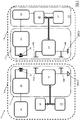
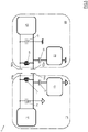
- the numeral 1 designates in its entirety a system for transferring electric energy and data according to embodiments of the present invention.
- the system 1 comprises a primary circuit 10 and a secondary circuit 20.
- the circuits 10 and 20 are physically separate and independent of each other.
- the primary circuit 10 is adapted to transfer electric energy and to exchange data with the secondary circuit 20 with a direct electrical connection between the two circuits.
- the primary circuit 10 can be included in a first stationary electronic device 30, such as a docking station, while the secondary circuit 20 can be included in a second portable electronic device 40 such as a cell phone, a smartphone, a table, a personal computer, a photo/video camera, etc.
- the adjective “primary” is used to indicate that the element to which it refers belongs to the primary circuit 10.
- the adjective “secondary” is used to indicate that the element to which it refers belongs to the secondary circuit 20.
- the primary circuit 10 comprises an electric energy source module - indicated as source module 11 hereafter -, a primary inductive element 12 - for example a transmission inductor or inductive coil, a primary transceiver module 13 and a pair of primary transceiving armatures, or more briefly primary armatures 14a and 14b.
- the source module 11 is connected to a power supply module 31 of the first device.
- the power supply module 31 comprises a battery, a power circuit and/or a wiring connected to a power supply grid, or else it can in turn draw the energy from another transmission system without electrical connections.
- the source module 11 comprises a DC/AC or AC/AC conversion circuitry - for example, a switching conversion circuit.
- the primary transceiving module 13 comprises a circuitry adapted to convert, or encode, data - for example, in binary format - into an electrical signal.
- the circuitry of the primary transceiving module 13 is adapted to execute also the inverse operation, i.e. to convert, or decode, electrical signals into data.
- the primary inductive element 12 is connected to the source module 11 through a respective pair of terminals.
- the primary transceiving module 13 is connected to both primary armatures 14a and 14b.
- the first primary armature 14a is connected to a first output terminal of the primary transceiving module 13, while the second primary armature 14b is connected to a second output terminal of the primary transceiving module 13, which is also connected to a reference terminal of the primary circuit 10.
- the primary transceiving module 13 is connected to a processor module 33 and/or to a memory module 35 - volatile and/or non-volatile - of the first device 30.
- the secondary circuit 20 comprises an electric energy conversion module - indicated as conversion module 21 hereafter -, a secondary inductive element 22 - for example a reception inductor or inductive coil, a secondary transceiver module 23 and a pair of secondary transceiving armatures, or more briefly secondary armatures 24a and 24b.
- the conversion module 21 comprises a circuitry adapted to transform a wave of electric voltage variable over time (AC) into another voltage, for example direct (DC), to power a load 41 - for example, a battery 43, one or more processing modules 45, one or more memory modules 47, or any other electrical load, including sensors, actuators or other electrical apparatus.
- the conversion module 21 can convert the wave of electric voltage variable over time (AC) into another wave that is variable over time (AC) with different characteristics of amplitude or frequency to power any type of electrical load that operates with alternating current, including resistive elements, electric motors or other electrical apparatuses.
- the secondary transceiving module 23 has a structure that substantially corresponds to the primary transceiving module 13, mutatis mutandis , and a description thereof will not be replicated for the sake of brevity.
- the secondary inductive element 22 is connected to the conversion module 21 through a respective pair of terminals.
- the secondary transceiving module 23 is connected to both secondary armatures 24a and 24b.
- first secondary transceiving armature indicated as first secondary armature 24a hereafter
- second secondary transceiving armature indicated as second secondary armature 24b hereafter
- the secondary transceiving module 23 is connected to the processing module 45 and/or to the memory module 47 of the second device 40 to receive from/send to said data modules, for example in binary format.
- the primary circuit 10 is adapted to transfer electric energy to the secondary circuit 20 through an inductive coupling.
- the primary circuit 10 and the secondary circuit 20 are adapted to exchange data through a capacitive coupling.
- the transfer of energy and the exchange of data are mutually independent and can be carried out simultaneously or at different instants in time.
- the source module 11 is configured to generate a primary electric wave S E1 variable over time with a first frequency f 1 predetermined or included within a predefined interval, preferably of the order of hundreds of KHz or of MHz.
- the primary electric wave S E1 excites the primary inductive element 12 which generates a corresponding electromagnetic field that is variable over time.
- This electromagnetic field is, at least partially, collected by the secondary inductive element 22 which in turns generates a secondary electric wave S E2 .
- the primary inductive element 12 and the secondary inductive element 22 are coupled inductively to each other - i.e., they operate substantially as a transformer - and allow the transfer of electric energy from the primary circuit 10 to the secondary circuit 20.
- the secondary electric wave S E2 powers the conversion module 21, which is adapted to convert the secondary electric wave S E2 itself and provide it to the load 41 of the second device 40 appropriately conditioned, for example converted into a different voltage of into an appropriate current.
- the conversion module 21 is adapted to convert the secondary voltage wave SE2 into a pair of power supply voltage V DD and power supply current I DD adapted to power the load 41 of the second device 40 and hence to supply electric energy to the load 41 through the pair of voltage and power supply current V DD and I DD .
- the primary transceiving module 13 receives data - for example a string or a sequence of strings of binary values - from the processor module 33 or from the memory module 35 of the first device 30 to be sent to the second device 40. Consequently, the primary transceiving module 13 converts (encodes) the data into a primary electrical signal S D1 variable over time with a predetermined second frequency f 2 - for example, included within a predefined interval, preferably in the order of some MHz or GHz.
- the second frequency f 2 is higher than the first frequency f 1 ; for example, the second frequency f 2 is higher by at least one order of magnitude, more preferably by two orders of magnitude, than the first frequency f 1 . It is also possible for the second frequency f 2 to be variable within an interval or bandwidth of frequencies, for example delimited by a minimum value of frequency f 2_min and a maximum value of frequency f 2_max , with the minimum value of frequency f 2_min preferably higher than the first frequency f 1 .
- the primary electrical signal S D1 is adapted to vary the electric charge accumulated on the primary armatures 14a and 14b generating a variable electrical field that causes a corresponding accumulation of charges of opposite sign on the secondary armatures 24a and 24b, thereby generating a secondary electrical signal S D2 .
- each primary armature 14a and 14b couples capacitively to the corresponding secondary armature 24a and 24b to form a corresponding capacitor C 1 and C 2 .
- a circuit is formed that connects the two transceiving modules 13 and 23 and makes it possible to transfer an electrical signal from the primary circuit 10 to the secondary circuit 20.
- one of the two primary armatures and one of the two secondary armatures can be connected to the reference node, and hence to the corresponding primary reference potential (GNDp), of the primary circuit 10 and to the corresponding secondary reference potential (GNDs), of the secondary circuit 20 in effect coupling the two reference potentials to the secondary frequency f 2 of transmission of the data signals.
- GNDp primary reference potential
- GNDs secondary reference potential
- the second secondary electrical signal S D2 is received by the secondary transceiving module 23 that converts (decodes) it into the data initially provided to the primary transceiving module 13. Subsequently, the secondary transceiving module 23 provides the data to the processing module 45 and/or a memory module 47 - volatile and/or non-volatile - of the second device 40.
- the capacitive coupling between the primary armatures 14a and 14b and the secondary armatures 24a and 24b can be used as a 'bridge' to couple a primary communication channel with a secondary communication channel so as to define a continuous (data) communication channel between the primary circuit 10 and the secondary circuit 20.
- the capacitive coupling can be used as a data communication means, alternative to those currently in use for the identification of the interconnected devices and for the feedback necessary for the inductive power regulation on the load present on the secondary.
- the capacitive coupling can be used to define a continuous communication channel between the primary circuit 10 and the secondary circuit 20 to exchange data between a communication channel selected between a wired connection such as USB, PCI Express, HDMI, Display Port, Ethernet, CAN, LIN, Flexray type, or any other known standard.
- a communication channel selected between a wired connection such as USB, PCI Express, HDMI, Display Port, Ethernet, CAN, LIN, Flexray type, or any other known standard.
- the capacitive coupling creates a virtual wiring that connects two portions of communication channel (for example two portions of USB cables) each included in a respective device 30 or 40, and connected to a respective transceiving module 13 or 23.
- the two transceiving modules 13 and 23 are configured to receive data encoded according to the standard of the selected communication channel, to convert them into the primary electrical signal S D1 and secondary electrical signal S D2 , respectively, and to decode the secondary electrical signal S D2 and the primary electrical signal S D1 received, respectively, anew into data coded according to the standard of the selected communication channel.
- this variant allows a secure and reliable data connection between the second electronic device 40, which comprises the secondary circuit 20, and one or more devices connected to the first electronic device 30, comprising the primary circuit 10, both through an additional capacitive coupling and through a wired coupling.
- a first electronic device 30, comprising the primary circuit 10 can be configured to operate from hubs for the exchange of data between two or more devices (like the second device 40) connected thereto.
- transceiving modules 13 and 23 are configured for the management of full duplex communication - i.e. they are able to transmit and receive data flows concurrently and independently.
- an embodiment (not illustrated herein) comprises an additional primary armature and an additional secondary armature able to be mutually coupled so as to define a third capacitor.
- an additional data exchange channel it is possible to define an additional data exchange channel and then to carry out a data transmission in parallel to a data reception from primary circuit 10 to secondary circuit 20, and vice versa.
- transceiving modules 13 and 23 configured to encode the (binary) data to be transmitted and the (binary) data received in a determined time interval in a single multilevel signal M, able to assume multiple levels or values of voltage.
- the transceiving module 13 encodes the (binary) data to be transmitted through the primary electrical signal S D1 (provided for example by the processing module 33) and the (binary) data contained in the secondary electrical signal S D2 received in a multilevel signal M 1 .
- the primary transceiving module 13 or, equivalently, the secondary transceiving module 23 is configured to generate the corresponding primary multilevel signal M 1 or secondary multilevel signal M 2 at a first value of voltage (in the corresponding communication time interval), for example 0 V, to indicate that a logic 0 is to be transmitted and, at the same time, a logic 0 has been received from the other secondary transceiving module 23, or primary transceiving module 13, respectively.
- a first value of voltage in the corresponding communication time interval
- the primary transceiving module 13 or, equivalently, the secondary transceiving module 23 is configured to impose a second value of voltage, for example 3.3 V, to the corresponding primary multilevel signal M 1 or secondary multilevel signal M 2 .
- the primary transceiving module 13 or the secondary transceiving module 23 transmits a logic 1
- the primary transceiving module 13 or, equivalently, the secondary transceiving module 23 is configured to generate the corresponding primary multilevel signal M 1 or secondary multilevel signal M 2 at a third value of voltage, for example 5 V.
- the configuration just described above it is possible to avoid the need for buffers to store the transmitted and received data, while still assuring the capability to manage a full duplex communication by means of the transceiving modules 13 and 23, still without raising the number of armatures required, hence effectively implementing a full duplex data exchange.
- the coding of the primary multilevel signa IM 1 and secondary multilevel signal M 2 according to the present invention makes it possible to represent the four possible combinations of sent/received binary data with only three levels of voltage.
- this reduced number of levels or values of voltage used makes it possible to assure good robustness against interference of the data transmission system by selecting the first value of voltage (0 V), the second values of voltage (3.3 V) and the third value of voltage (5 V) at as great a distance from each other as possible with respect to the available power supply dynamics (such as a power supply voltage of 5 V in the case of the numerical examples provided above).
- the transceiving modules 13 and 23 it is possible to configure the transceiving modules 13 and 23 to generate the corresponding primary multilevel signal M 1 or secondary multilevel signal M 2 so as to associate the information of the logic values of the data received and transmitted to the transition from a value of voltage or to another value of voltage instead of to the values themselves.
- the information of the logic values of the data received and transmitted is contained in the wavefronts of the primary multilevel signal M 1 or secondary multilevel signal M 2 generated by the transceiving modules 13 and 23.
- the Applicant has found that it is possible to form one or both of the primary armatures 14a and 14b, and one or both of the secondary armatures 24a and 24b with solutions adapted to maintain compact the structures of the primary circuit 10 and of the secondary circuit 20, while maintaining high efficiency and effectiveness both of the energy transfer and of the data exchange, and keeping the costs comparable to those typical of the inductive energy transmission system alone.
- the primary armatures 14a and 14b, and the secondary armatures 24a and 24b comprise a conductive element having two predominant dimensions with respect to the third dimension - for example planar.
- each primary armature 14a and 14b and each secondary armature 24a and 24b comprises a pad of conductive material - such as copper - provided on a support surface.
- the support surface can for example be independent insulating material - polymeric or ceramic, or also a printed circuit board - or the electric board on which the components of the primary circuit 10 and of the secondary circuit 20 are mounted, respectively.
- a plate of copper of aluminium or a metal frame can advantageously be used as a conductive material adapted to produce the primary armatures 14a and 14b, and secondary armatures 24a and 24b without requiring a dedicated support surface.
- planar conductive element can be produced with the same techniques and materials with which the inductive elements are formed 12 and 22, if the latter are inductors drawn on a printed circuit board and not traditional inductors obtained by means of wound wires.
- the primary armatures 14a and 14b, and secondary armatures 24a and 24b can be formed in proximity to or distant from the inductive elements 12 and 22, respectively, according to the specific application. Typically, it is opportune and advantageous to provide the primary armatures 14a and 14b, and the secondary armatures 24a and 24b in proximity to the inductive elements 12 and 22, or integrated therein, to obtain the primary circuit 10 and the secondary circuit 20 with particularly compact structures.
- the primary armatures 14a and 14b, and the secondary armatures 24a and 24b and the inductive elements 12 and 22 are planar shaped - although nothing prohibits shaping them with any shape to be adapted to the application - for example planar for smartphones, cylindrical for items like electric toothbrushes, remove controls or other electrical appliances, etcetera.
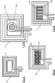
- At least one of the primary armatures 14a or 14b comprises a planar conductive element 50 positioned inside a region delimited by the primary inductive element 12.
- at least one of the secondary transceiving armatures 24a or 24b comprises a planar conductive element (not shown) positioned inside a region delimited by the secondary inductive element 22.
- the primary armature 14a and secondary armature 24a which, in use, are coupled to form the corresponding capacitor C 1 or the primary armature 14b and the secondary armature 24b which, in use, are coupled to form the corresponding capacitor C 2 comprise the planar conductive element formed in the region delimited by the respective inductive element 12 or 22.
- said conductive elements are shaped with a same surface area.
- the arrangement of the planar conductive elements 50 assures a rotational or translational alignment freedom between the primary circuit 10 and the secondary circuit 20.
- the primary 14a and secondary 24a armatures shaped as described above are coupled to form the capacitor C 1 regardless of a relative orientation or positioning of the primary circuit 10 and of the secondary circuit 20.
- the capacity of the capacitor C 1 is substantially uniform - at the limit, within a predetermined range of values - regardless of the relative orientation or positioning of the primary circuit 10 and of the secondary circuit 20.
- both primary armatures 14a and 14b can comprise respective conductive elements formed in the region delimited by the inductive element 12.
- the secondary armatures 24a and 24b too can comprise respective conductive elements formed, in a similar manner, in the region delimited by the inductive element 22.
- each of the primary armatures 14a and 14b comprises respective planar conductive elements 51a and 51b shaped concentric to each other in the region delimited by the inductive element 12.
- a similar arrangement must be provided in the corresponding secondary armatures 24a and 24b. In this way, freedom of angular positioning of the secondary element with respect to the primary element is assured.
- each of the primary armatures 14a and 14b comprises a plurality of planar conductive elements 52a and 52b shaped with a checkerboard arrangement - i.e., arranged alternating along two mutually perpendicular axes - in the region delimited by the inductive element 12.
- a similar arrangement must be provided in the corresponding secondary armatures 24a and 24b. In this way, freedom of translational positioning along two Cartesian axes of the secondary element with respect to the primary element is assured.
- each of the primary armatures 14a and 14b comprises a plurality of planar conductive elements 53a and 53b shaped with a side by side arrangement - i.e., arranged alternating along a predetermined and preferential direction - in the region delimited by the inductive element 12.
- a similar arrangement must be provided in the secondary armatures 24a and 24b.
- the arrangement of the planar conductive elements 50, 51a and 51b, 52a and 52b, and 53a and 53b assures a rotational or translational freedom between the primary circuit 10 and the secondary circuit 20.
- the primary armatures 14a and 14b and the armatures 24a and 24b shaped as described above are coupled to form the capacitors C 1 and C 2 in a substantially independent manner of a relative orientation of the primary circuit 10 and of the secondary circuit 20.
- the capacity of the capacitors C 1 and C 2 is substantially uniform - at the limit, within a predetermined range of values - regardless of the relative orientation of the primary circuit 10 and of the secondary circuit 20.
- the total surface areas of the planar conductive elements 51a, 52a and 53a correspond to the total surface areas of the planar conductive elements 51b, 52b and 53b, respectively, so as to define capacitors C 1 and C 2 with substantially equal capacities when the primary armatures 14a and 14b the armatures 24a and 24b are coupled.
- planar conductive elements can be obtained with an open loop or comb structure.
- planar conductive elements 54 and 55 are obtained according to a 'multifingered' structure.
- each of the planar conductive elements 54 and 55 comprising pluralities of elongated portions 541 and 551 or 'fingers', respectively, which are distanced and separate from in each other so as not to form loops.
- These multifingered planar conductive elements 54 and 55 allow to maintain high the total surface area of the armature 14a, 14b, 24a or 24b thus obtained, maximising the coupling capacity, while allowing to abate and possibly eliminate the emergence of parasitic current - in particular, the so-called eddy currents, also known as Foucault currents - generated in the armatures 14a, 14b, 24a or 24b by the variable magnetic field generated by the inductive elements 12 and 22 traversed by the current for the transfer of energy.
- eddy currents also known as Foucault currents - generated in the armatures 14a, 14b, 24a or 24b by the variable magnetic field generated by the inductive elements 12 and 22 traversed by the current for the transfer of energy.
- the abatement of the parasitic currents induced by the magnetic field avoids or lowers the probability of a false detection of a spurious object - i.e. a conductive object different from, or not including, the secondary circuit 20 - by a protection/energy saving circuitry - known in the art as Foreign Object Detection, FOD, and not described in detail herein - which can be integrated in the primary circuit 10 (or in the device 30).
- each conductive element - in particular, multifingered conductive elements 54 and 55 and conductive elements 51a, 52a and 53a - is made with a track of electrically conductive material with width of the order of a mm or tens of mm.
- traces of such dimensions allow to define multifingered conductive elements 54 and 55 adapted to form C 1 and C 2 with capacity of a value adapted for capacitive data transfer at a frequency f 2 of high value, preferably with a value of capacity from a pF to a nF.
- each conductive element 50, 51a, 52a and 53a, 54 and 55 can be obtained with a track of conductive material with reduced thickness, for example equal to or smaller than 50 ⁇ m, preferably smaller than 1 ⁇ m.
- the inductive elements 12 and 22 too can be obtained with a track made of electrically conductive material, possibly but not necessarily with thickness equal or similar to the conductive elements 50, 51a, 52a, 53a, 54 and 55. These dimensions allow further to limit the size of the parasitic currents, to obtain with a single support inductive coils and capacitive armatures and to minimise other parasitic effects like the skin effect.
- one or more of the primary armatures 14a and 14b and/or of the secondary armatures 24a and 24b can be implemented exploiting circuit portions of the primary circuit 10 and of the secondary circuit 20 - or portions of the first device 30 and of the second device 40, respectively - having a different main purpose.
- one or both of the primary armatures 14a or 14b of the system 1 are defined by a respective primary circuit portion and one or both of the corresponding secondary armatures are defined by a respective secondary circuit portion.
- Each primary circuit portion and each respective secondary circuit portion although they have a different main purpose, are adapted or are made adapted also to interact with each other defining a capacitor C 1 or C 2 of predetermined capacity.
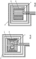
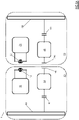
- a first primary circuit portion 61a comprises a portion of the primary inductive element 12 proximal to a first connection terminal 121 included in the primary inductive element 12, provided - together with a second terminal 122 - for connection with other circuit components, such as the source module 11.
- a second primary circuit portion 61 is also exploited, which comprises a portion of the primary inductive element 12 proximal to the second connection terminal 122.
- the extension of the primary circuit portions 61a and 61b depend on a working frequency of the data exchange operation, i.e. the second frequency f 2 , and on the inductance of the respective inductive element 12 and 22.
- a central portion 63 of the inductive element 12 or 22 behaves like an open circuit at the second frequency f 2 electrically separating the primary circuit portions 61 from each other.
- the extension of the secondary circuit portions 62a and 62b substantially corresponds to the extension of the primary circuit portions 61a and 61b given the coupled operation of the inductive elements 12 and 22.
- the primary circuit portions 61a and 61b are connected to each other by means of a primary bridge capacitor 71 and to the reference terminal by means of a primary tail capacitor 71.
- the secondary circuit portions 62a and 62b are connected to each other by means of a secondary bridge capacitor 73 and to the reference terminal by means of a secondary tail capacitor 74.
- the capacitors 71, 72, 73 and 74 are dimensioned so as to operate substantially as short-circuits at the second frequency f 2 and as open circuits at the first frequency f 1 .
- the primary portions 61a and 61b define the second primary armature 14b in series to the transceiving module 13 through the respective reference terminal, and the secondary circuit portions 62a and 62b define the second secondary armatures 24b in series to the transceiving module 23 through the respective reference terminal.
- the actual capacity of the capacity C 2 formed by the coupling between the armatures 14b and 24b depends on the extension of the primary circuit portions 61a and 62b and of the secondary circuit portions 62a and 62b, on their distance and on the dimensions of the conductive filament that composes the inductive elements 12 and 22.
- the inductive element 12 (as well as, similarly, the inductive element 22 not shown) has a planar format; therefore, a width w of the track of conductive material that defines it contributes to determine the capacity of the capacity C 2 .
- the inductive elements 12 and 22 formed with known technologies allow to define a capacitor C 2 . with capacity between a few pF to the order of some nF according to implementation needs without requiring particular expedients in the construction of the system 1.
- the electrical separation given by the central part of the inductor at the frequency f 2 allows to exploit as independent circuit portions each segment of the inductive elements 12 and 22 that is proximal to a respective terminal.
- the primary circuit portions 61a and 61b are used independently of each other and the corresponding two secondary circuit portions 62a and 62b are used independently of each other.
- the first primary portion 61a is connected to the primary transceiving module 13 through a bridge capacitor 72, while the second primary portion 61b is connected to the reference terminal through a tail capacitor 71.
- the first secondary portion 62a is connected to the secondary transceiving module 23 through a bridge capacitor 77, while the second secondary portion 62b is connected to the reference terminal through a tail capacitor 78.
- the capacitors 75, 76, 77 and 78 are dimensioned so as to operate substantially as short-circuits at the second frequency f2and as open circuits at the first frequency f 1 .
- the first primary portion 61a defines the first primary armature 14a
- the second primary portion 61b defines the second primary armature 14b
- the first secondary portion 62a defines the first secondary armature 24a
- the second secondary portion 62b defines the second secondary armature 24b.
- the inductive elements 12 and 22 formed with known technologies allow to define the capacitors C 1 and C 2 with respective capacities between a few pF to the order of some nF according to implementation needs without requiring particular expedients in the construction of the system 1.
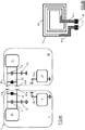
- one of the primary armatures 14a or 14b and the corresponding secondary armature 24a or 24b are formed exploiting a part 80 and 90 of the first device 30 and of the second device 40, respectively, in particular a portion made of conductive material of a respective casing or frame, of an EMI shielding element or a ground plane of the first device 30 and of the second device 40.
- a part 80 and 90 of the first device 30 and of the second device 40 respectively, in particular a portion made of conductive material of a respective casing or frame, of an EMI shielding element or a ground plane of the first device 30 and of the second device 40.
- each part 80 and 90 of the first device 30 and of the second device 40 is connected to the respective transceiver module 13 and 23 through a corresponding bridge capacitor 81 and 91, while the first primary 14a and secondary 14b armatures are formed as described above in particular relation to Figure 2A in which a planar conductive element 50 is formed in the area delimited by the corresponding inductive element 12 or 21; however, nothing precludes forming the first primary armature 14a and the second primary armature 24a according to different techniques.
- the first primary armature 14a and the first secondary armature 24a can be obtained exploiting the primary circuit portion 61, and the secondary circuit portion 62 of the inductive elements 12 and 22, respectively, as described above for example in relation to Figures 4A and 4B , so as to exploit the capacitive coupling between said circuit portions to obtain a corresponding first capacitor C 1 of desired capacity.
- the primary circuit portions 61a and 61b are connected to each other and to the primary transceiving module 13 through respective bridge capacitors 82 and 83.
- the secondary circuit portions 62a and 62b are connected to each other and to the secondary transceiving module 23 through respective bridge capacitors 92 and 93.
- the capacitors 81-83 and the capacitors 91 - 93 are dimensioned so as to operate substantially as short-circuits at the second frequency f 2 and as open circuits at the first frequency f 1 .
- both capacitors C 1 and C 2 of desired capacity are implemented using mutually different circuit portions with reduced construction complexity simply introducing a small number of capacitors.
- each circuit 10 and 20 As respective first armature 14a and 14b, and for example the ground plane of each circuit 10 and 20 as respective second pad 24a and 24b so as to obtain a capacitive coupling adapted to the exchange of data without providing armatures dedicated to this purpose.
- the applicant has observed that it is possible to optimise the dimensions of the parts 80 and 90 of the first device 30 and of the second device 40, for example of the planes of mass and/or power supply, to obtain a capacitive coupling area adapted to allow a reliable and efficient data exchange between the primary circuit 10 and the secondary circuit 20 without comprising the original purpose of the parts 80 and 90.
- a primary armature for example the first primary armature 14a
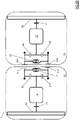
- a shielding element 100 which can be included in the primary circuit 10 configured to attenuate the magnetic field produced by the inductive elements 12 and 22 in the regions where said inductive elements are not spatially superposed - to abate, or at least attenuate, interference phenomena.
- the shielding element 100 is connected to the primary transceiving module 13 through a bridge capacitor 101, while it is connected to the reference node through an inductor 102.
- the capacitor 101 is dimensioned so as to operate substantially as a short-circuit at the second frequency f 2 and as an open circuit at the first frequency f 1 .
- the inductor 102 is dimensioned so as to operate substantially as a short-circuit at the first frequency f 1 and at frequencies lower than f 2 , and as an open circuit at the second frequency f 2 .
- the shielding element 110 is connected to the secondary transceiving module 23 through a bridge capacitor 111, while it is connected to the reference node through an inductor 112.
- the capacitor 111 is dimensioned so as to operate substantially as a short-circuit at the second frequency f 2 and as an open circuit at the first frequency f 1 .
- the inductor 112 is dimensioned so as to operate substantially as a short-circuit at the first frequency f 1 and at frequencies lower than f 2 , and as an open circuit at the second frequency f 2 .
- the invention thus conceived is susceptible of numerous modifications and variants without departing from the scope of the inventive concept.
- the shapes, the dimensions and the layout of the inductive elements - and, hence, of any circuit portions that can be mutually coupled - can vary according to design specifications and/or implementative requirements.
- the shapes, the dimensions and the layouts of any pads formed circumscribed by said inductive elements will vary according to design specifications and/or implementative requirements.
- armature pads can be formed that circumscribe the inductive elements in addition or alternatively to the pads circumscribed by said elements. Otherwise, nothing precludes forming inductive elements and armatures with different structures from the planar ones as inductive elements comprising wire windings and/or armatures formed by plates made of conductive materials.
- the system 1 comprises at least one of the primary armatures formed by a plurality of planar conductive elements as shown in Figure 2C or in Figure 2D and is configured to sense the planar conductive elements implementing an appropriate method of distinguishing them (for example, by an arrangement configured to provide an appropriately calibrated measure of impedance, or through an exchange of information between primary circuit and secondary circuit, preferably according to a dedicated appropriate protocol).
- the system can configure a part, for example half, of the planar conductive elements of the primary circuit to excite the first secondary armature, and another part, for example the second half, of planar conductive elements of the primary circuit to excite the second secondary armature with a signal of opposite phase or simply closing the data circuit at the reference terminal.
- the planar conductive elements of the primary armatures must be in a higher number than the planar conductive elements of the secondary armatures; moreover, the planar conductive elements of the primary armatures are preferably formed with a smaller dimension of the conductive elements of the secondary armatures.
- an armature formed by a shielding element can be coupled to an armature defined by a pad circumscribed by an inductive element or by one or both of the circuit portions associated with the inductive element.
- a coupled capacitor can be formed by corresponding elements of the devices comprising the primary and secondary circuit and the other capacitor can comprise an armature defined by the shielding element.
Landscapes
- Engineering & Computer Science (AREA)
- Computer Networks & Wireless Communication (AREA)
- Power Engineering (AREA)
- Signal Processing (AREA)
- Physics & Mathematics (AREA)
- Electromagnetism (AREA)
- Near-Field Transmission Systems (AREA)
- Exchange Systems With Centralized Control (AREA)
Claims (10)
- System (1) zum Übertragen von elektrischer Energie und Daten, umfassend einen Primärkreislauf (10) und einen Sekundärkreislauf (20), wobeia) der Primärkreislauf (10) Folgendes umfasst:i) ein Quellenmodul elektrischer Energie (11);ii) ein primäres induktives Element (12), das mit dem Quellenmodul (11) verbunden ist und ein Paar von Verbindungsanschlüssen (121, 122) umfasst;iii) ein primäres Sendeempfängermodul (13), das konfiguriert ist, um Daten in elektromagnetische Signale zu kodieren und um elektromagnetische Signale in Daten zu dekodieren, undiv) ein Paar von primären Sendeempfängerarmaturen (14a, 14b), die mit dem primären Sendeempfängermodul (13) verbunden sind,b) wobei der Sekundärkreislauf (20) Folgendes umfasst:i) ein Umwandlungsmodul elektrischer Energie (21);ii) ein sekundäres induktives Element (22), das mit dem Umwandlungsmodul (21) verbunden ist und ein Paar von Verbindungsanschlüssen umfasst;iii) ein sekundäres Sendeempfängermodul (23), das konfiguriert ist, um Daten in elektromagnetische Signale zu kodieren und um elektromagnetische Signale in Daten zu dekodieren, undiv) ein Paar von sekundären Sendeempfängerarmaturen (24a, 24b), die mit dem sekundären Sendeempfängermodul (23) verbunden sind,wobei das primäre induktive Element (12) und das sekundäre induktive Element (22) konfiguriert sind, um gegenseitig induktiv gekoppelt zu sein, was eine Übertragung von elektrischer Energie von dem Quellenmodul (11) zu dem Umwandlungsmodul (21) ermöglicht, und wobei jede primäre Sendeempfängerarmatur (14a, 14b) konfiguriert ist, um kapazitiv mit einer jeweiligen sekundären Sendeempfängerarmatur (24a, 24b) gekoppelt zu sein, was einen Austausch von Daten zwischen dem primären Sendeempfängermodul (13) und dem sekundären Sendeempfängermodul (23) ermöglicht,wobei mindestens einer (14a) von den ersten primären Sendeempfängerarmaturen (14a, 14b) durch einen primären Schaltungsabschnitt (61a, 61b) definiert ist, und mindestens eine entsprechende erste sekundäre Sendeempfängerarmatur (24a) durch einen sekundären Schaltungsabschnitt (62a, 62b) definiert ist,wobei der primäre Schaltungsabschnitt (61a, 61b) und der sekundäre Schaltungsabschnitt (62a, 62b) konfiguriert sind, um gegenseitig zu koppeln und einen Kondensator mit vorbestimmter Kapazität zu definieren,wobei der primäre Schaltungsabschnitt (61a, 61b) einen Abschnitt des primären induktiven Elements (12) in der Nähe von einem der Verbindungsanschlüsse (121, 122) des primären induktiven Elements (12) umfasst, undwobei der sekundäre Schaltungsabschnitt (62a, 62b) einen Abschnitt des sekundären induktiven Elements (22) in der Nähe von einem der Verbindungsanschlüsse des sekundären induktiven Elements (22) umfasst.
- System (1) nach Anspruch 1, wobei das primäre Sendeempfängermodul (13) mit einem Verbindungsanschluss des primären induktiven Elements verbunden ist und das sekundäre Sendeempfängermodul (23) mit einem Verbindungsanschluss des sekundären induktiven Elements (22) verbunden ist.
- System (1) nach Anspruch 1 oder 2, wobei eine zweite primäre Sendeempfängerarmatur (14b) durch einen zusätzlichen primären Schaltungsabschnitt (61b) definiert ist, und wobei eine zweite sekundäre Sendeempfängerarmatur (24b) durch einen zusätzlichen sekundären Schaltungsabschnitt (62b) definiert ist, und wobei der zusätzliche primäre Schaltungsabschnitt (61b) und der zusätzliche sekundäre Schaltungsabschnitt (62b) konfiguriert sind, um miteinander zu interagieren und einen zusätzlichen Kondensator mit vorbestimmter Kapazität zu definieren.
- System (1) nach einem der vorherigen Ansprüche, wobei mindestens eine primäre Sendeempfängerarmatur (14a, 14b) ein leitendes Element (50; 51a; 52a; 53a; 54; 55) umfasst, das innerhalb eines Bereichs angeordnet ist, der durch das primäre induktive Element (12) begrenzt ist, und mindestens eine sekundäre Sendeempfängerarmatur (24b) ein leitendes Element umfasst, das innerhalb eines Bereichs angeordnet ist, der durch das sekundäre induktive Element (22) begrenzt ist.
- System (1) nach Anspruch 4, wobei jedes leitende Element (54, 55) eine offene Schleifenform aufweist.
- System (1) nach Anspruch 4 oder 5, wobei jedes leitende Element (50; 51a, 51b; 52a, 52b; 53a, 53b; 54; 55) mit einer Bahn aus leitendem Material mit einer Stärke in der Größenordnung von Zehntel- oder Hundertstelmillimetern erlangt wird.
- System (1) nach einem der vorherigen Ansprüche, wobei der Primärkreislauf (10) in eine erste elektronische Vorrichtung (30) aufgenommen ist und der Sekundärkreislauf (20) in eine zweite elektronische Vorrichtung (40) aufgenommen ist, und bei dem die zweite elektronische Vorrichtung (40) von der ersten elektronischen Vorrichtung (30) getrennt und in Bezug darauf beweglich ist.
- System (1) nach Anspruch 7, wobei die erste elektronische Vorrichtung (30) mindestens ein primäres Verarbeitungsmodul (33) umfasst, das mit dem primären Sendeempfängermodul (13) verbunden und konfiguriert ist, um damit Daten im Binärformat auszutauschen, und wobei die zweite elektronische Vorrichtung (40) ein sekundäres Verarbeitungsmodul (45) umfasst, das mit dem sekundären Sendeempfängermodul (23) verbunden und konfiguriert ist, um damit Daten in Binärformat auszutauschen.
- System (1) nach Anspruch 7 oder 8, wobei die erste Vorrichtung einen primären Kommunikationskanal umfasst, der mit dem primären Sendeempfängermodul (13) verbunden ist, um damit Daten auszutauschen, die gemäß dem Standard des Kommunikationskanals kodiert sind, und wobei die zweite elektronische Vorrichtung (40) einen sekundären Kommunikationskanal umfasst, der mit dem primären Sendeempfängermodul (13) verbunden ist, um damit Daten auszutauschen, die gemäß dem Standard des Kommunikationskanals kodiert sind, wobei der primäre Kommunikationskanal und der sekundäre Kommunikationskanal zu einer gleichen Technologie gehören, die ausgewählt ist aus: USB, I2C, SPI, PCI Express, HDMI, Display Port, Ethernet, CAN, LIN, Flexray oder andere standardmäßige Kommunikationsbusse.
- Verfahren zum Vollduplex-Datenaustausch über das System (1) nach einem der vorherigen Ansprüche, umfassend:a) Empfangen, an dem primären Sendemodul (13) oder an dem sekundären Sendeempfängermodul (23), von ersten binären Daten die an das sekundäre Sendemodul (23) bzw. an das primäre Sendeempfängermodul (13) gesendet werden sollen;b) Empfangen, an dem primären Sendemodul (13) oder an dem sekundären Sendeempfängermodul (23), von zweiten binären Daten, die über die kapazitive Kopplung zwischen den primären Sendeempfängerarmaturen (14a, 14b) und den jeweiligen sekundären Sendeempfängerarmaturen (24a, 24b) von dem sekundären Sendemodul (23) bzw. von dem primären Sendeempfängermodul (23) gesendet werden, undc) Erzeugen eines Mehrstufensignals, das Folgendes aufweist:i) einen ersten Spannungswert, wenn sowohl die ersten binären Daten als auch die zweiten binären Daten einen logischen Wert 0 darstellen,ii) einen zweiten Spannungswert, wenn sowohl die ersten binären Daten als auch die zweiten binären Daten unterschiedliche logische Werte darstellen, oderiii) einen dritten Spannungswert, wenn sowohl die ersten binären Daten als auch die zweiten binären Daten einen logischen Wert 1 darstellen.
Applications Claiming Priority (2)
| Application Number | Priority Date | Filing Date | Title |
|---|---|---|---|
| IT102018000006612A IT201800006612A1 (it) | 2018-06-25 | 2018-06-25 | Sistema per trasferimento di energia e scambio dati tra dispositivi elettronici |
| PCT/IB2019/054668 WO2020003027A1 (en) | 2018-06-25 | 2019-06-05 | System for transferring energy and exchanging data between electronic devices |
Publications (2)
| Publication Number | Publication Date |
|---|---|
| EP3811491A1 EP3811491A1 (de) | 2021-04-28 |
| EP3811491B1 true EP3811491B1 (de) | 2022-05-11 |
Family
ID=63579710
Family Applications (1)
| Application Number | Title | Priority Date | Filing Date |
|---|---|---|---|
| EP19742904.6A Active EP3811491B1 (de) | 2018-06-25 | 2019-06-05 | System zum übertragen von energie und zum austausch von daten zwischen elektronischen geräten |
Country Status (8)
| Country | Link |
|---|---|
| US (1) | US11108269B2 (de) |
| EP (1) | EP3811491B1 (de) |
| JP (1) | JP7154320B2 (de) |
| KR (1) | KR102476560B1 (de) |
| CN (1) | CN112313855B (de) |
| IT (1) | IT201800006612A1 (de) |
| TW (1) | TWI799592B (de) |
| WO (1) | WO2020003027A1 (de) |
Families Citing this family (3)
| Publication number | Priority date | Publication date | Assignee | Title |
|---|---|---|---|---|
| IT202000009202A1 (it) * | 2020-04-28 | 2021-10-28 | Eggtronic Eng S P A | Base di alimentazione elettrica |
| JP7713679B2 (ja) * | 2020-12-28 | 2025-07-28 | エルジー ディスプレイ カンパニー リミテッド | 伝送システム、伝送ケーブル、伝送方法、および表示装置 |
| EP4730371A1 (de) * | 2024-10-21 | 2026-04-22 | Power Integrations, Inc. | Kapazitive koppler und systeme mit kapazitiven kopplern |
Family Cites Families (20)
| Publication number | Priority date | Publication date | Assignee | Title |
|---|---|---|---|---|
| US5451763A (en) * | 1994-07-05 | 1995-09-19 | Alto Corporation | Personal medical IC card and read/write unit |
| DE4436592C2 (de) * | 1994-10-13 | 1996-11-07 | Mueller & Weigert | Galvanisch getrennte Daten- und Energieübertragung |
| DE19705301C1 (de) * | 1997-02-13 | 1998-10-01 | V W B Gmbh | Einrichtung zur berührungslosen Informations- und Energieübertragung |
| ATE298949T1 (de) * | 2000-04-18 | 2005-07-15 | Schleifring Und Appbau Gmbh | Anordnung zur übertragung elektrischer energie bzw. eines signals |
| US20070159329A1 (en) * | 2005-12-02 | 2007-07-12 | Shmuel Silverman | Information protection using a printed electronic circuit and laser impression |
| JP5415780B2 (ja) * | 2009-02-20 | 2014-02-12 | 健一 原川 | 電力供給システム、及びそのための可動体と固定体 |
| JP5478326B2 (ja) * | 2010-03-30 | 2014-04-23 | パナソニック株式会社 | 非接触給電システム |
| TWI589086B (zh) * | 2012-03-21 | 2017-06-21 | 莫喬流動公司 | 用於無線電力傳輸之系統及方法 |
| JP5867601B2 (ja) * | 2012-06-15 | 2016-02-24 | 株式会社村田製作所 | 電力伝送システム及び送電装置 |
| EP3402063A1 (de) * | 2013-02-08 | 2018-11-14 | Markus Rehm | Drahtlose resonanzgekoppelte elektrische energieübertragung |
| JP2015077021A (ja) * | 2013-10-10 | 2015-04-20 | ソニー株式会社 | 受電装置および送電装置ならびに給電システム |
| DK3161934T3 (da) * | 2014-06-26 | 2019-12-16 | Eggtronic Eng S R L | Fremgangsmåde og apparat til overførsel af elektrisk effekt |
| US20160191085A1 (en) * | 2014-08-13 | 2016-06-30 | Skyworks Solutions, Inc. | Transmit front end module for dual antenna applications |
| US10079508B2 (en) * | 2015-01-22 | 2018-09-18 | Integrated Device Technology, Inc. | Apparatuses and related methods for detecting magnetic flux field characteristics with a wireless power receiver |
| ITUB20153094A1 (it) * | 2015-08-12 | 2017-02-12 | Eggtronic Eng S R L | Metodo ed apparato per trasferire potenza elettrica e dati |
| CN107920752B (zh) * | 2015-09-03 | 2025-01-10 | 皇家飞利浦有限公司 | 用于无线交换数据和功率的电池模块 |
| JP6466624B2 (ja) * | 2015-09-03 | 2019-02-06 | コーニンクレッカ フィリップス エヌ ヴェKoninklijke Philips N.V. | デバイスを接続してデバイス間のデータ及び/又は電力のワイヤレス交換を可能にするためのケーブルユニット |
| EP3168953A1 (de) * | 2015-11-13 | 2017-05-17 | TE Connectivity Germany GmbH | Kontaktfreies verbindersystem mit rückmeldung von sekundärseite |
| EP3182555B1 (de) * | 2015-12-18 | 2019-04-17 | TE Connectivity Nederland B.V. | Kontaktfreier verbinder und kontaktfreies verbindersystem |
| US10310110B2 (en) * | 2017-02-21 | 2019-06-04 | Geospace Technologies Corporation | Systems and methods for seismic data acquisition |
-
2018
- 2018-06-25 IT IT102018000006612A patent/IT201800006612A1/it unknown
-
2019
- 2019-05-31 TW TW108119059A patent/TWI799592B/zh active
- 2019-06-05 EP EP19742904.6A patent/EP3811491B1/de active Active
- 2019-06-05 KR KR1020207034329A patent/KR102476560B1/ko active Active
- 2019-06-05 WO PCT/IB2019/054668 patent/WO2020003027A1/en not_active Ceased
- 2019-06-05 JP JP2020570794A patent/JP7154320B2/ja active Active
- 2019-06-05 US US15/734,428 patent/US11108269B2/en active Active
- 2019-06-05 CN CN201980042289.4A patent/CN112313855B/zh active Active
Also Published As
| Publication number | Publication date |
|---|---|
| JP7154320B2 (ja) | 2022-10-17 |
| US20210226477A1 (en) | 2021-07-22 |
| EP3811491A1 (de) | 2021-04-28 |
| KR102476560B1 (ko) | 2022-12-12 |
| CN112313855A (zh) | 2021-02-02 |
| CN112313855B (zh) | 2021-10-12 |
| KR20210024450A (ko) | 2021-03-05 |
| JP2021531716A (ja) | 2021-11-18 |
| US11108269B2 (en) | 2021-08-31 |
| TWI799592B (zh) | 2023-04-21 |
| IT201800006612A1 (it) | 2019-12-25 |
| TW202019057A (zh) | 2020-05-16 |
| WO2020003027A1 (en) | 2020-01-02 |
Similar Documents
| Publication | Publication Date | Title |
|---|---|---|
| KR101524966B1 (ko) | 무선 전력 환경에서의 시그널링 충전 | |
| US10075018B2 (en) | Wireless power receiver | |
| CN108156829B (zh) | 无线电力发送器及其控制方法 | |
| USRE50160E1 (en) | Wireless power receiver | |
| US11108269B2 (en) | System for transferring energy and exchanging data between electronic devices | |
| US20200204003A1 (en) | Power relay device and system | |
| WO2017155693A1 (en) | Method and apparatus for adapting wireless power transfer between wireless power protocols | |
| WO2021227652A1 (zh) | 无线充电设备和待充电设备 | |
| CN114530949B (zh) | 一种无线充电的发射端、充电底座及系统 | |
| CN110635581A (zh) | 一种可折叠的磁谐振耦合无线电能传输系统的收发天线 | |
| KR20140067443A (ko) | 무선 전력 수신기 | |
| HK40037030B (en) | System for transferring energy and exchanging data between electronic devices | |
| HK40037030A (en) | System for transferring energy and exchanging data between electronic devices | |
| CN113396520A (zh) | 一种无线电力接收电路 | |
| CN115189483B (zh) | 一种线圈模组及电子设备 | |
| Hao | Principles, Current Status, and Optimization of Multi-Device Wireless Charging Systems | |
| CN210899209U (zh) | 一种可将家用普通设备接入ZigBee物联网的转换器 | |
| CN211930692U (zh) | 一种实时双向无线信号传输的无线供电监控相机 | |
| CN104866090A (zh) | 基于无线能量传输的无线人体交互装置 |
Legal Events
| Date | Code | Title | Description |
|---|---|---|---|
| STAA | Information on the status of an ep patent application or granted ep patent |
Free format text: STATUS: UNKNOWN |
|
| STAA | Information on the status of an ep patent application or granted ep patent |
Free format text: STATUS: THE INTERNATIONAL PUBLICATION HAS BEEN MADE |
|
| PUAI | Public reference made under article 153(3) epc to a published international application that has entered the european phase |
Free format text: ORIGINAL CODE: 0009012 |
|
| STAA | Information on the status of an ep patent application or granted ep patent |
Free format text: STATUS: REQUEST FOR EXAMINATION WAS MADE |
|
| 17P | Request for examination filed |
Effective date: 20201123 |
|
| AK | Designated contracting states |
Kind code of ref document: A1 Designated state(s): AL AT BE BG CH CY CZ DE DK EE ES FI FR GB GR HR HU IE IS IT LI LT LU LV MC MK MT NL NO PL PT RO RS SE SI SK SM TR |
|
| AX | Request for extension of the european patent |
Extension state: BA ME |
|
| DAV | Request for validation of the european patent (deleted) | ||
| DAX | Request for extension of the european patent (deleted) | ||
| GRAP | Despatch of communication of intention to grant a patent |
Free format text: ORIGINAL CODE: EPIDOSNIGR1 |
|
| STAA | Information on the status of an ep patent application or granted ep patent |
Free format text: STATUS: GRANT OF PATENT IS INTENDED |
|
| INTG | Intention to grant announced |
Effective date: 20220103 |
|
| GRAS | Grant fee paid |
Free format text: ORIGINAL CODE: EPIDOSNIGR3 |
|
| GRAA | (expected) grant |
Free format text: ORIGINAL CODE: 0009210 |
|
| STAA | Information on the status of an ep patent application or granted ep patent |
Free format text: STATUS: THE PATENT HAS BEEN GRANTED |
|
| AK | Designated contracting states |
Kind code of ref document: B1 Designated state(s): AL AT BE BG CH CY CZ DE DK EE ES FI FR GB GR HR HU IE IS IT LI LT LU LV MC MK MT NL NO PL PT RO RS SE SI SK SM TR |
|
| REG | Reference to a national code |
Ref country code: GB Ref legal event code: FG4D |
|
| REG | Reference to a national code |
Ref country code: CH Ref legal event code: EP |
|
| REG | Reference to a national code |
Ref country code: AT Ref legal event code: REF Ref document number: 1492305 Country of ref document: AT Kind code of ref document: T Effective date: 20220515 |
|
| REG | Reference to a national code |
Ref country code: DE Ref legal event code: R096 Ref document number: 602019014921 Country of ref document: DE |
|
| REG | Reference to a national code |
Ref country code: IE Ref legal event code: FG4D |
|
| PGFP | Annual fee paid to national office [announced via postgrant information from national office to epo] |
Ref country code: NL Payment date: 20220626 Year of fee payment: 4 Ref country code: MC Payment date: 20220520 Year of fee payment: 4 Ref country code: LU Payment date: 20220627 Year of fee payment: 4 Ref country code: IE Payment date: 20220627 Year of fee payment: 4 |
|
| REG | Reference to a national code |
Ref country code: NL Ref legal event code: FP |
|
| PGFP | Annual fee paid to national office [announced via postgrant information from national office to epo] |
Ref country code: BE Payment date: 20220627 Year of fee payment: 4 |
|
| REG | Reference to a national code |
Ref country code: LT Ref legal event code: MG9D |
|
| REG | Reference to a national code |
Ref country code: AT Ref legal event code: MK05 Ref document number: 1492305 Country of ref document: AT Kind code of ref document: T Effective date: 20220511 |
|
| PG25 | Lapsed in a contracting state [announced via postgrant information from national office to epo] |
Ref country code: SE Free format text: LAPSE BECAUSE OF FAILURE TO SUBMIT A TRANSLATION OF THE DESCRIPTION OR TO PAY THE FEE WITHIN THE PRESCRIBED TIME-LIMIT Effective date: 20220511 Ref country code: PT Free format text: LAPSE BECAUSE OF FAILURE TO SUBMIT A TRANSLATION OF THE DESCRIPTION OR TO PAY THE FEE WITHIN THE PRESCRIBED TIME-LIMIT Effective date: 20220912 Ref country code: NO Free format text: LAPSE BECAUSE OF FAILURE TO SUBMIT A TRANSLATION OF THE DESCRIPTION OR TO PAY THE FEE WITHIN THE PRESCRIBED TIME-LIMIT Effective date: 20220811 Ref country code: LT Free format text: LAPSE BECAUSE OF FAILURE TO SUBMIT A TRANSLATION OF THE DESCRIPTION OR TO PAY THE FEE WITHIN THE PRESCRIBED TIME-LIMIT Effective date: 20220511 Ref country code: HR Free format text: LAPSE BECAUSE OF FAILURE TO SUBMIT A TRANSLATION OF THE DESCRIPTION OR TO PAY THE FEE WITHIN THE PRESCRIBED TIME-LIMIT Effective date: 20220511 Ref country code: GR Free format text: LAPSE BECAUSE OF FAILURE TO SUBMIT A TRANSLATION OF THE DESCRIPTION OR TO PAY THE FEE WITHIN THE PRESCRIBED TIME-LIMIT Effective date: 20220812 Ref country code: FI Free format text: LAPSE BECAUSE OF FAILURE TO SUBMIT A TRANSLATION OF THE DESCRIPTION OR TO PAY THE FEE WITHIN THE PRESCRIBED TIME-LIMIT Effective date: 20220511 Ref country code: BG Free format text: LAPSE BECAUSE OF FAILURE TO SUBMIT A TRANSLATION OF THE DESCRIPTION OR TO PAY THE FEE WITHIN THE PRESCRIBED TIME-LIMIT Effective date: 20220811 Ref country code: AT Free format text: LAPSE BECAUSE OF FAILURE TO SUBMIT A TRANSLATION OF THE DESCRIPTION OR TO PAY THE FEE WITHIN THE PRESCRIBED TIME-LIMIT Effective date: 20220511 |
|
| PGFP | Annual fee paid to national office [announced via postgrant information from national office to epo] |
Ref country code: TR Payment date: 20220811 Year of fee payment: 4 |
|
| PG25 | Lapsed in a contracting state [announced via postgrant information from national office to epo] |
Ref country code: RS Free format text: LAPSE BECAUSE OF FAILURE TO SUBMIT A TRANSLATION OF THE DESCRIPTION OR TO PAY THE FEE WITHIN THE PRESCRIBED TIME-LIMIT Effective date: 20220511 Ref country code: PL Free format text: LAPSE BECAUSE OF FAILURE TO SUBMIT A TRANSLATION OF THE DESCRIPTION OR TO PAY THE FEE WITHIN THE PRESCRIBED TIME-LIMIT Effective date: 20220511 Ref country code: LV Free format text: LAPSE BECAUSE OF FAILURE TO SUBMIT A TRANSLATION OF THE DESCRIPTION OR TO PAY THE FEE WITHIN THE PRESCRIBED TIME-LIMIT Effective date: 20220511 Ref country code: IS Free format text: LAPSE BECAUSE OF FAILURE TO SUBMIT A TRANSLATION OF THE DESCRIPTION OR TO PAY THE FEE WITHIN THE PRESCRIBED TIME-LIMIT Effective date: 20220911 |
|
| PGFP | Annual fee paid to national office [announced via postgrant information from national office to epo] |
Ref country code: CH Payment date: 20220706 Year of fee payment: 4 |
|
| PG25 | Lapsed in a contracting state [announced via postgrant information from national office to epo] |
Ref country code: SM Free format text: LAPSE BECAUSE OF FAILURE TO SUBMIT A TRANSLATION OF THE DESCRIPTION OR TO PAY THE FEE WITHIN THE PRESCRIBED TIME-LIMIT Effective date: 20220511 Ref country code: SK Free format text: LAPSE BECAUSE OF FAILURE TO SUBMIT A TRANSLATION OF THE DESCRIPTION OR TO PAY THE FEE WITHIN THE PRESCRIBED TIME-LIMIT Effective date: 20220511 Ref country code: RO Free format text: LAPSE BECAUSE OF FAILURE TO SUBMIT A TRANSLATION OF THE DESCRIPTION OR TO PAY THE FEE WITHIN THE PRESCRIBED TIME-LIMIT Effective date: 20220511 Ref country code: ES Free format text: LAPSE BECAUSE OF FAILURE TO SUBMIT A TRANSLATION OF THE DESCRIPTION OR TO PAY THE FEE WITHIN THE PRESCRIBED TIME-LIMIT Effective date: 20220511 Ref country code: EE Free format text: LAPSE BECAUSE OF FAILURE TO SUBMIT A TRANSLATION OF THE DESCRIPTION OR TO PAY THE FEE WITHIN THE PRESCRIBED TIME-LIMIT Effective date: 20220511 Ref country code: DK Free format text: LAPSE BECAUSE OF FAILURE TO SUBMIT A TRANSLATION OF THE DESCRIPTION OR TO PAY THE FEE WITHIN THE PRESCRIBED TIME-LIMIT Effective date: 20220511 Ref country code: CZ Free format text: LAPSE BECAUSE OF FAILURE TO SUBMIT A TRANSLATION OF THE DESCRIPTION OR TO PAY THE FEE WITHIN THE PRESCRIBED TIME-LIMIT Effective date: 20220511 |
|
| REG | Reference to a national code |
Ref country code: DE Ref legal event code: R097 Ref document number: 602019014921 Country of ref document: DE |
|
| PLBE | No opposition filed within time limit |
Free format text: ORIGINAL CODE: 0009261 |
|
| STAA | Information on the status of an ep patent application or granted ep patent |
Free format text: STATUS: NO OPPOSITION FILED WITHIN TIME LIMIT |
|
| PG25 | Lapsed in a contracting state [announced via postgrant information from national office to epo] |
Ref country code: AL Free format text: LAPSE BECAUSE OF FAILURE TO SUBMIT A TRANSLATION OF THE DESCRIPTION OR TO PAY THE FEE WITHIN THE PRESCRIBED TIME-LIMIT Effective date: 20220511 |
|
| 26N | No opposition filed |
Effective date: 20230214 |
|
| PG25 | Lapsed in a contracting state [announced via postgrant information from national office to epo] |
Ref country code: SI Free format text: LAPSE BECAUSE OF FAILURE TO SUBMIT A TRANSLATION OF THE DESCRIPTION OR TO PAY THE FEE WITHIN THE PRESCRIBED TIME-LIMIT Effective date: 20220511 |
|
| PG25 | Lapsed in a contracting state [announced via postgrant information from national office to epo] |
Ref country code: MC Free format text: LAPSE BECAUSE OF NON-PAYMENT OF DUE FEES Effective date: 20230630 |
|
| PG25 | Lapsed in a contracting state [announced via postgrant information from national office to epo] |
Ref country code: MC Free format text: LAPSE BECAUSE OF NON-PAYMENT OF DUE FEES Effective date: 20230630 |
|
| REG | Reference to a national code |
Ref country code: CH Ref legal event code: PL |
|
| REG | Reference to a national code |
Ref country code: NL Ref legal event code: MM Effective date: 20230701 |
|
| REG | Reference to a national code |
Ref country code: BE Ref legal event code: MM Effective date: 20230630 |
|
| PG25 | Lapsed in a contracting state [announced via postgrant information from national office to epo] |
Ref country code: LU Free format text: LAPSE BECAUSE OF NON-PAYMENT OF DUE FEES Effective date: 20230605 |
|
| REG | Reference to a national code |
Ref country code: IE Ref legal event code: MM4A |
|
| PG25 | Lapsed in a contracting state [announced via postgrant information from national office to epo] |
Ref country code: NL Free format text: LAPSE BECAUSE OF NON-PAYMENT OF DUE FEES Effective date: 20230701 Ref country code: LU Free format text: LAPSE BECAUSE OF NON-PAYMENT OF DUE FEES Effective date: 20230605 |
|
| PG25 | Lapsed in a contracting state [announced via postgrant information from national office to epo] |
Ref country code: IE Free format text: LAPSE BECAUSE OF NON-PAYMENT OF DUE FEES Effective date: 20230605 |
|
| PG25 | Lapsed in a contracting state [announced via postgrant information from national office to epo] |
Ref country code: MK Free format text: LAPSE BECAUSE OF FAILURE TO SUBMIT A TRANSLATION OF THE DESCRIPTION OR TO PAY THE FEE WITHIN THE PRESCRIBED TIME-LIMIT Effective date: 20220511 Ref country code: IE Free format text: LAPSE BECAUSE OF NON-PAYMENT OF DUE FEES Effective date: 20230605 Ref country code: CY Free format text: LAPSE BECAUSE OF FAILURE TO SUBMIT A TRANSLATION OF THE DESCRIPTION OR TO PAY THE FEE WITHIN THE PRESCRIBED TIME-LIMIT Effective date: 20220511 Ref country code: CH Free format text: LAPSE BECAUSE OF NON-PAYMENT OF DUE FEES Effective date: 20230630 |
|
| PG25 | Lapsed in a contracting state [announced via postgrant information from national office to epo] |
Ref country code: HU Free format text: LAPSE BECAUSE OF FAILURE TO SUBMIT A TRANSLATION OF THE DESCRIPTION OR TO PAY THE FEE WITHIN THE PRESCRIBED TIME-LIMIT; INVALID AB INITIO Effective date: 20190605 Ref country code: BE Free format text: LAPSE BECAUSE OF NON-PAYMENT OF DUE FEES Effective date: 20230630 |
|
| PGFP | Annual fee paid to national office [announced via postgrant information from national office to epo] |
Ref country code: IT Payment date: 20240326 Year of fee payment: 6 |
|
| PGFP | Annual fee paid to national office [announced via postgrant information from national office to epo] |
Ref country code: GB Payment date: 20240627 Year of fee payment: 6 |
|
| PGFP | Annual fee paid to national office [announced via postgrant information from national office to epo] |
Ref country code: DE Payment date: 20240627 Year of fee payment: 6 |
|
| PGFP | Annual fee paid to national office [announced via postgrant information from national office to epo] |
Ref country code: FR Payment date: 20240625 Year of fee payment: 6 |
|
| PG25 | Lapsed in a contracting state [announced via postgrant information from national office to epo] |
Ref country code: MT Free format text: LAPSE BECAUSE OF FAILURE TO SUBMIT A TRANSLATION OF THE DESCRIPTION OR TO PAY THE FEE WITHIN THE PRESCRIBED TIME-LIMIT Effective date: 20220511 |
|
| PG25 | Lapsed in a contracting state [announced via postgrant information from national office to epo] |
Ref country code: BG Free format text: LAPSE BECAUSE OF FAILURE TO SUBMIT A TRANSLATION OF THE DESCRIPTION OR TO PAY THE FEE WITHIN THE PRESCRIBED TIME-LIMIT Effective date: 20220511 |
|
| PG25 | Lapsed in a contracting state [announced via postgrant information from national office to epo] |
Ref country code: BG Free format text: LAPSE BECAUSE OF FAILURE TO SUBMIT A TRANSLATION OF THE DESCRIPTION OR TO PAY THE FEE WITHIN THE PRESCRIBED TIME-LIMIT Effective date: 20220511 |
|
| REG | Reference to a national code |
Ref country code: DE Ref legal event code: R119 Ref document number: 602019014921 Country of ref document: DE |
|
| GBPC | Gb: european patent ceased through non-payment of renewal fee |
Effective date: 20250605 |
|
| PG25 | Lapsed in a contracting state [announced via postgrant information from national office to epo] |
Ref country code: GB Free format text: LAPSE BECAUSE OF NON-PAYMENT OF DUE FEES Effective date: 20250605 |
|
| PG25 | Lapsed in a contracting state [announced via postgrant information from national office to epo] |
Ref country code: DE Free format text: LAPSE BECAUSE OF NON-PAYMENT OF DUE FEES Effective date: 20260101 |
|
| PG25 | Lapsed in a contracting state [announced via postgrant information from national office to epo] |
Ref country code: IT Free format text: LAPSE BECAUSE OF NON-PAYMENT OF DUE FEES Effective date: 20250605 |
|
| PG25 | Lapsed in a contracting state [announced via postgrant information from national office to epo] |
Ref country code: FR Free format text: LAPSE BECAUSE OF NON-PAYMENT OF DUE FEES Effective date: 20250630 |