EP3806598A1 - Radio wave absorbing member, radio wave absorbing structure, and inspection device - Google Patents
Radio wave absorbing member, radio wave absorbing structure, and inspection device Download PDFInfo
- Publication number
- EP3806598A1 EP3806598A1 EP20817640.4A EP20817640A EP3806598A1 EP 3806598 A1 EP3806598 A1 EP 3806598A1 EP 20817640 A EP20817640 A EP 20817640A EP 3806598 A1 EP3806598 A1 EP 3806598A1
- Authority
- EP
- European Patent Office
- Prior art keywords
- radio wave
- wave absorbing
- absorbing member
- layer
- support
- Prior art date
- Legal status (The legal status is an assumption and is not a legal conclusion. Google has not performed a legal analysis and makes no representation as to the accuracy of the status listed.)
- Withdrawn
Links
Images


Classifications
-
- H—ELECTRICITY
- H05—ELECTRIC TECHNIQUES NOT OTHERWISE PROVIDED FOR
- H05K—PRINTED CIRCUITS; CASINGS OR CONSTRUCTIONAL DETAILS OF ELECTRIC APPARATUS; MANUFACTURE OF ASSEMBLAGES OF ELECTRICAL COMPONENTS
- H05K9/00—Screening of apparatus or components against electric or magnetic fields
- H05K9/0073—Shielding materials
- H05K9/0081—Electromagnetic shielding materials, e.g. EMI, RFI shielding
- H05K9/0088—Electromagnetic shielding materials, e.g. EMI, RFI shielding comprising a plurality of shielding layers; combining different shielding material structure
-
- H—ELECTRICITY
- H01—ELECTRIC ELEMENTS
- H01Q—ANTENNAS, i.e. RADIO AERIALS
- H01Q17/00—Devices for absorbing waves radiated from an antenna; Combinations of such devices with active antenna elements or systems
- H01Q17/004—Devices for absorbing waves radiated from an antenna; Combinations of such devices with active antenna elements or systems using non-directional dissipative particles, e.g. ferrite powders
-
- B—PERFORMING OPERATIONS; TRANSPORTING
- B32—LAYERED PRODUCTS
- B32B—LAYERED PRODUCTS, i.e. PRODUCTS BUILT-UP OF STRATA OF FLAT OR NON-FLAT, e.g. CELLULAR OR HONEYCOMB, FORM
- B32B15/00—Layered products comprising a layer of metal
- B32B15/04—Layered products comprising a layer of metal comprising metal as the main or only constituent of a layer, which is next to another layer of the same or of a different material
- B32B15/08—Layered products comprising a layer of metal comprising metal as the main or only constituent of a layer, which is next to another layer of the same or of a different material of synthetic resin
- B32B15/09—Layered products comprising a layer of metal comprising metal as the main or only constituent of a layer, which is next to another layer of the same or of a different material of synthetic resin comprising polyesters
-
- B—PERFORMING OPERATIONS; TRANSPORTING
- B32—LAYERED PRODUCTS
- B32B—LAYERED PRODUCTS, i.e. PRODUCTS BUILT-UP OF STRATA OF FLAT OR NON-FLAT, e.g. CELLULAR OR HONEYCOMB, FORM
- B32B15/00—Layered products comprising a layer of metal
- B32B15/20—Layered products comprising a layer of metal comprising aluminium or copper
-
- B—PERFORMING OPERATIONS; TRANSPORTING
- B32—LAYERED PRODUCTS
- B32B—LAYERED PRODUCTS, i.e. PRODUCTS BUILT-UP OF STRATA OF FLAT OR NON-FLAT, e.g. CELLULAR OR HONEYCOMB, FORM
- B32B27/00—Layered products comprising a layer of synthetic resin
- B32B27/06—Layered products comprising a layer of synthetic resin as the main or only constituent of a layer, which is next to another layer of the same or of a different material
-
- B—PERFORMING OPERATIONS; TRANSPORTING
- B32—LAYERED PRODUCTS
- B32B—LAYERED PRODUCTS, i.e. PRODUCTS BUILT-UP OF STRATA OF FLAT OR NON-FLAT, e.g. CELLULAR OR HONEYCOMB, FORM
- B32B27/00—Layered products comprising a layer of synthetic resin
- B32B27/06—Layered products comprising a layer of synthetic resin as the main or only constituent of a layer, which is next to another layer of the same or of a different material
- B32B27/065—Layered products comprising a layer of synthetic resin as the main or only constituent of a layer, which is next to another layer of the same or of a different material of foam
-
- B—PERFORMING OPERATIONS; TRANSPORTING
- B32—LAYERED PRODUCTS
- B32B—LAYERED PRODUCTS, i.e. PRODUCTS BUILT-UP OF STRATA OF FLAT OR NON-FLAT, e.g. CELLULAR OR HONEYCOMB, FORM
- B32B27/00—Layered products comprising a layer of synthetic resin
- B32B27/06—Layered products comprising a layer of synthetic resin as the main or only constituent of a layer, which is next to another layer of the same or of a different material
- B32B27/08—Layered products comprising a layer of synthetic resin as the main or only constituent of a layer, which is next to another layer of the same or of a different material of synthetic resin
-
- B—PERFORMING OPERATIONS; TRANSPORTING
- B32—LAYERED PRODUCTS
- B32B—LAYERED PRODUCTS, i.e. PRODUCTS BUILT-UP OF STRATA OF FLAT OR NON-FLAT, e.g. CELLULAR OR HONEYCOMB, FORM
- B32B27/00—Layered products comprising a layer of synthetic resin
- B32B27/06—Layered products comprising a layer of synthetic resin as the main or only constituent of a layer, which is next to another layer of the same or of a different material
- B32B27/10—Layered products comprising a layer of synthetic resin as the main or only constituent of a layer, which is next to another layer of the same or of a different material of paper or cardboard
-
- B—PERFORMING OPERATIONS; TRANSPORTING
- B32—LAYERED PRODUCTS
- B32B—LAYERED PRODUCTS, i.e. PRODUCTS BUILT-UP OF STRATA OF FLAT OR NON-FLAT, e.g. CELLULAR OR HONEYCOMB, FORM
- B32B27/00—Layered products comprising a layer of synthetic resin
- B32B27/28—Layered products comprising a layer of synthetic resin comprising synthetic resins not wholly covered by any one of the sub-groups B32B27/30 - B32B27/42
- B32B27/281—Layered products comprising a layer of synthetic resin comprising synthetic resins not wholly covered by any one of the sub-groups B32B27/30 - B32B27/42 comprising polyimides
-
- B—PERFORMING OPERATIONS; TRANSPORTING
- B32—LAYERED PRODUCTS
- B32B—LAYERED PRODUCTS, i.e. PRODUCTS BUILT-UP OF STRATA OF FLAT OR NON-FLAT, e.g. CELLULAR OR HONEYCOMB, FORM
- B32B27/00—Layered products comprising a layer of synthetic resin
- B32B27/30—Layered products comprising a layer of synthetic resin comprising vinyl (co)polymers; comprising acrylic (co)polymers
- B32B27/304—Layered products comprising a layer of synthetic resin comprising vinyl (co)polymers; comprising acrylic (co)polymers comprising vinyl halide (co)polymers, e.g. PVC, PVDC, PVF, PVDF
-
- B—PERFORMING OPERATIONS; TRANSPORTING
- B32—LAYERED PRODUCTS
- B32B—LAYERED PRODUCTS, i.e. PRODUCTS BUILT-UP OF STRATA OF FLAT OR NON-FLAT, e.g. CELLULAR OR HONEYCOMB, FORM
- B32B27/00—Layered products comprising a layer of synthetic resin
- B32B27/30—Layered products comprising a layer of synthetic resin comprising vinyl (co)polymers; comprising acrylic (co)polymers
- B32B27/308—Layered products comprising a layer of synthetic resin comprising vinyl (co)polymers; comprising acrylic (co)polymers comprising acrylic (co)polymers
-
- B—PERFORMING OPERATIONS; TRANSPORTING
- B32—LAYERED PRODUCTS
- B32B—LAYERED PRODUCTS, i.e. PRODUCTS BUILT-UP OF STRATA OF FLAT OR NON-FLAT, e.g. CELLULAR OR HONEYCOMB, FORM
- B32B27/00—Layered products comprising a layer of synthetic resin
- B32B27/32—Layered products comprising a layer of synthetic resin comprising polyolefins
-
- B—PERFORMING OPERATIONS; TRANSPORTING
- B32—LAYERED PRODUCTS
- B32B—LAYERED PRODUCTS, i.e. PRODUCTS BUILT-UP OF STRATA OF FLAT OR NON-FLAT, e.g. CELLULAR OR HONEYCOMB, FORM
- B32B27/00—Layered products comprising a layer of synthetic resin
- B32B27/32—Layered products comprising a layer of synthetic resin comprising polyolefins
- B32B27/325—Layered products comprising a layer of synthetic resin comprising polyolefins comprising polycycloolefins
-
- B—PERFORMING OPERATIONS; TRANSPORTING
- B32—LAYERED PRODUCTS
- B32B—LAYERED PRODUCTS, i.e. PRODUCTS BUILT-UP OF STRATA OF FLAT OR NON-FLAT, e.g. CELLULAR OR HONEYCOMB, FORM
- B32B27/00—Layered products comprising a layer of synthetic resin
- B32B27/36—Layered products comprising a layer of synthetic resin comprising polyesters
-
- B—PERFORMING OPERATIONS; TRANSPORTING
- B32—LAYERED PRODUCTS
- B32B—LAYERED PRODUCTS, i.e. PRODUCTS BUILT-UP OF STRATA OF FLAT OR NON-FLAT, e.g. CELLULAR OR HONEYCOMB, FORM
- B32B27/00—Layered products comprising a layer of synthetic resin
- B32B27/36—Layered products comprising a layer of synthetic resin comprising polyesters
- B32B27/365—Layered products comprising a layer of synthetic resin comprising polyesters comprising polycarbonates
-
- B—PERFORMING OPERATIONS; TRANSPORTING
- B32—LAYERED PRODUCTS
- B32B—LAYERED PRODUCTS, i.e. PRODUCTS BUILT-UP OF STRATA OF FLAT OR NON-FLAT, e.g. CELLULAR OR HONEYCOMB, FORM
- B32B27/00—Layered products comprising a layer of synthetic resin
- B32B27/40—Layered products comprising a layer of synthetic resin comprising polyurethanes
-
- B—PERFORMING OPERATIONS; TRANSPORTING
- B32—LAYERED PRODUCTS
- B32B—LAYERED PRODUCTS, i.e. PRODUCTS BUILT-UP OF STRATA OF FLAT OR NON-FLAT, e.g. CELLULAR OR HONEYCOMB, FORM
- B32B29/00—Layered products comprising a layer of paper or cardboard
- B32B29/08—Corrugated paper or cardboard
-
- B—PERFORMING OPERATIONS; TRANSPORTING
- B32—LAYERED PRODUCTS
- B32B—LAYERED PRODUCTS, i.e. PRODUCTS BUILT-UP OF STRATA OF FLAT OR NON-FLAT, e.g. CELLULAR OR HONEYCOMB, FORM
- B32B3/00—Layered products comprising a layer with external or internal discontinuities or unevennesses, or a layer of non-planar shape; Layered products comprising a layer having particular features of form
- B32B3/26—Layered products comprising a layer with external or internal discontinuities or unevennesses, or a layer of non-planar shape; Layered products comprising a layer having particular features of form characterised by a particular shape of the outline of the cross-section of a continuous layer; characterised by a layer with cavities or internal voids ; characterised by an apertured layer
- B32B3/28—Layered products comprising a layer with external or internal discontinuities or unevennesses, or a layer of non-planar shape; Layered products comprising a layer having particular features of form characterised by a particular shape of the outline of the cross-section of a continuous layer; characterised by a layer with cavities or internal voids ; characterised by an apertured layer characterised by a layer comprising a deformed thin sheet, i.e. the layer having its entire thickness deformed out of the plane, e.g. corrugated, crumpled
-
- B—PERFORMING OPERATIONS; TRANSPORTING
- B32—LAYERED PRODUCTS
- B32B—LAYERED PRODUCTS, i.e. PRODUCTS BUILT-UP OF STRATA OF FLAT OR NON-FLAT, e.g. CELLULAR OR HONEYCOMB, FORM
- B32B33/00—Layered products characterised by particular properties or particular surface features, e.g. particular surface coatings; Layered products designed for particular purposes not covered by another single class
-
- B—PERFORMING OPERATIONS; TRANSPORTING
- B32—LAYERED PRODUCTS
- B32B—LAYERED PRODUCTS, i.e. PRODUCTS BUILT-UP OF STRATA OF FLAT OR NON-FLAT, e.g. CELLULAR OR HONEYCOMB, FORM
- B32B5/00—Layered products characterised by the non- homogeneity or physical structure, i.e. comprising a fibrous, filamentary, particulate or foam layer; Layered products characterised by having a layer differing constitutionally or physically in different parts
- B32B5/18—Layered products characterised by the non- homogeneity or physical structure, i.e. comprising a fibrous, filamentary, particulate or foam layer; Layered products characterised by having a layer differing constitutionally or physically in different parts characterised by features of a layer of foamed material
-
- B—PERFORMING OPERATIONS; TRANSPORTING
- B32—LAYERED PRODUCTS
- B32B—LAYERED PRODUCTS, i.e. PRODUCTS BUILT-UP OF STRATA OF FLAT OR NON-FLAT, e.g. CELLULAR OR HONEYCOMB, FORM
- B32B7/00—Layered products characterised by the relation between layers; Layered products characterised by the relative orientation of features between layers, or by the relative values of a measurable parameter between layers, i.e. products comprising layers having different physical, chemical or physicochemical properties; Layered products characterised by the interconnection of layers
- B32B7/04—Interconnection of layers
- B32B7/12—Interconnection of layers using interposed adhesives or interposed materials with bonding properties
-
- C—CHEMISTRY; METALLURGY
- C08—ORGANIC MACROMOLECULAR COMPOUNDS; THEIR PREPARATION OR CHEMICAL WORKING-UP; COMPOSITIONS BASED THEREON
- C08J—WORKING-UP; GENERAL PROCESSES OF COMPOUNDING; AFTER-TREATMENT NOT COVERED BY SUBCLASSES C08B, C08C, C08F, C08G or C08H
- C08J7/00—Chemical treatment or coating of shaped articles made of macromolecular substances
- C08J7/04—Coating
- C08J7/06—Coating with compositions not containing macromolecular substances
-
- H—ELECTRICITY
- H01—ELECTRIC ELEMENTS
- H01Q—ANTENNAS, i.e. RADIO AERIALS
- H01Q17/00—Devices for absorbing waves radiated from an antenna; Combinations of such devices with active antenna elements or systems
-
- H—ELECTRICITY
- H01—ELECTRIC ELEMENTS
- H01Q—ANTENNAS, i.e. RADIO AERIALS
- H01Q17/00—Devices for absorbing waves radiated from an antenna; Combinations of such devices with active antenna elements or systems
- H01Q17/008—Devices for absorbing waves radiated from an antenna; Combinations of such devices with active antenna elements or systems with a particular shape
-
- H—ELECTRICITY
- H05—ELECTRIC TECHNIQUES NOT OTHERWISE PROVIDED FOR
- H05K—PRINTED CIRCUITS; CASINGS OR CONSTRUCTIONAL DETAILS OF ELECTRIC APPARATUS; MANUFACTURE OF ASSEMBLAGES OF ELECTRICAL COMPONENTS
- H05K9/00—Screening of apparatus or components against electric or magnetic fields
- H05K9/0073—Shielding materials
- H05K9/0081—Electromagnetic shielding materials, e.g. EMI, RFI shielding
-
- B—PERFORMING OPERATIONS; TRANSPORTING
- B32—LAYERED PRODUCTS
- B32B—LAYERED PRODUCTS, i.e. PRODUCTS BUILT-UP OF STRATA OF FLAT OR NON-FLAT, e.g. CELLULAR OR HONEYCOMB, FORM
- B32B2255/00—Coating on the layer surface
- B32B2255/10—Coating on the layer surface on synthetic resin layer or on natural or synthetic rubber layer
-
- B—PERFORMING OPERATIONS; TRANSPORTING
- B32—LAYERED PRODUCTS
- B32B—LAYERED PRODUCTS, i.e. PRODUCTS BUILT-UP OF STRATA OF FLAT OR NON-FLAT, e.g. CELLULAR OR HONEYCOMB, FORM
- B32B2255/00—Coating on the layer surface
- B32B2255/20—Inorganic coating
-
- B—PERFORMING OPERATIONS; TRANSPORTING
- B32—LAYERED PRODUCTS
- B32B—LAYERED PRODUCTS, i.e. PRODUCTS BUILT-UP OF STRATA OF FLAT OR NON-FLAT, e.g. CELLULAR OR HONEYCOMB, FORM
- B32B2264/00—Composition or properties of particles which form a particulate layer or are present as additives
- B32B2264/02—Synthetic macromolecular particles
- B32B2264/0214—Particles made of materials belonging to B32B27/00
- B32B2264/0228—Vinyl resin particles, e.g. polyvinyl acetate, polyvinyl alcohol polymers or ethylene-vinyl acetate copolymers
- B32B2264/0235—Aromatic vinyl resin, e.g. styrenic (co)polymers
-
- B—PERFORMING OPERATIONS; TRANSPORTING
- B32—LAYERED PRODUCTS
- B32B—LAYERED PRODUCTS, i.e. PRODUCTS BUILT-UP OF STRATA OF FLAT OR NON-FLAT, e.g. CELLULAR OR HONEYCOMB, FORM
- B32B2264/00—Composition or properties of particles which form a particulate layer or are present as additives
- B32B2264/10—Inorganic particles
- B32B2264/102—Oxide or hydroxide
-
- B—PERFORMING OPERATIONS; TRANSPORTING
- B32—LAYERED PRODUCTS
- B32B—LAYERED PRODUCTS, i.e. PRODUCTS BUILT-UP OF STRATA OF FLAT OR NON-FLAT, e.g. CELLULAR OR HONEYCOMB, FORM
- B32B2266/00—Composition of foam
- B32B2266/02—Organic
- B32B2266/0214—Materials belonging to B32B27/00
- B32B2266/0221—Vinyl resin
- B32B2266/0228—Aromatic vinyl resin, e.g. styrenic (co)polymers
-
- B—PERFORMING OPERATIONS; TRANSPORTING
- B32—LAYERED PRODUCTS
- B32B—LAYERED PRODUCTS, i.e. PRODUCTS BUILT-UP OF STRATA OF FLAT OR NON-FLAT, e.g. CELLULAR OR HONEYCOMB, FORM
- B32B2266/00—Composition of foam
- B32B2266/02—Organic
- B32B2266/0214—Materials belonging to B32B27/00
- B32B2266/0242—Acrylic resin
-
- B—PERFORMING OPERATIONS; TRANSPORTING
- B32—LAYERED PRODUCTS
- B32B—LAYERED PRODUCTS, i.e. PRODUCTS BUILT-UP OF STRATA OF FLAT OR NON-FLAT, e.g. CELLULAR OR HONEYCOMB, FORM
- B32B2266/00—Composition of foam
- B32B2266/02—Organic
- B32B2266/0214—Materials belonging to B32B27/00
- B32B2266/025—Polyolefin
-
- B—PERFORMING OPERATIONS; TRANSPORTING
- B32—LAYERED PRODUCTS
- B32B—LAYERED PRODUCTS, i.e. PRODUCTS BUILT-UP OF STRATA OF FLAT OR NON-FLAT, e.g. CELLULAR OR HONEYCOMB, FORM
- B32B2266/00—Composition of foam
- B32B2266/02—Organic
- B32B2266/0214—Materials belonging to B32B27/00
- B32B2266/0264—Polyester
-
- B—PERFORMING OPERATIONS; TRANSPORTING
- B32—LAYERED PRODUCTS
- B32B—LAYERED PRODUCTS, i.e. PRODUCTS BUILT-UP OF STRATA OF FLAT OR NON-FLAT, e.g. CELLULAR OR HONEYCOMB, FORM
- B32B2307/00—Properties of the layers or laminate
- B32B2307/20—Properties of the layers or laminate having particular electrical or magnetic properties, e.g. piezoelectric
-
- B—PERFORMING OPERATIONS; TRANSPORTING
- B32—LAYERED PRODUCTS
- B32B—LAYERED PRODUCTS, i.e. PRODUCTS BUILT-UP OF STRATA OF FLAT OR NON-FLAT, e.g. CELLULAR OR HONEYCOMB, FORM
- B32B2307/00—Properties of the layers or laminate
- B32B2307/30—Properties of the layers or laminate having particular thermal properties
- B32B2307/306—Resistant to heat
- B32B2307/3065—Flame resistant or retardant, fire resistant or retardant
-
- B—PERFORMING OPERATIONS; TRANSPORTING
- B32—LAYERED PRODUCTS
- B32B—LAYERED PRODUCTS, i.e. PRODUCTS BUILT-UP OF STRATA OF FLAT OR NON-FLAT, e.g. CELLULAR OR HONEYCOMB, FORM
- B32B2307/00—Properties of the layers or laminate
- B32B2307/50—Properties of the layers or laminate having particular mechanical properties
- B32B2307/546—Flexural strength; Flexion stiffness
-
- B—PERFORMING OPERATIONS; TRANSPORTING
- B32—LAYERED PRODUCTS
- B32B—LAYERED PRODUCTS, i.e. PRODUCTS BUILT-UP OF STRATA OF FLAT OR NON-FLAT, e.g. CELLULAR OR HONEYCOMB, FORM
- B32B2307/00—Properties of the layers or laminate
- B32B2307/70—Other properties
- B32B2307/718—Weight, e.g. weight per square meter
-
- B—PERFORMING OPERATIONS; TRANSPORTING
- B32—LAYERED PRODUCTS
- B32B—LAYERED PRODUCTS, i.e. PRODUCTS BUILT-UP OF STRATA OF FLAT OR NON-FLAT, e.g. CELLULAR OR HONEYCOMB, FORM
- B32B2307/00—Properties of the layers or laminate
- B32B2307/70—Other properties
- B32B2307/732—Dimensional properties
-
- C—CHEMISTRY; METALLURGY
- C08—ORGANIC MACROMOLECULAR COMPOUNDS; THEIR PREPARATION OR CHEMICAL WORKING-UP; COMPOSITIONS BASED THEREON
- C08J—WORKING-UP; GENERAL PROCESSES OF COMPOUNDING; AFTER-TREATMENT NOT COVERED BY SUBCLASSES C08B, C08C, C08F, C08G or C08H
- C08J2367/00—Characterised by the use of polyesters obtained by reactions forming a carboxylic ester link in the main chain; Derivatives of such polymers
- C08J2367/02—Polyesters derived from dicarboxylic acids and dihydroxy compounds
Definitions
- the present invention relates to a radio wave absorbing member, a radio wave absorbing structure, and an inspection apparatus.
- ⁇ /4 radio wave absorbers have been known. ⁇ /4 radio wave absorbers show a higher return loss than that of other radio wave absorbers such as magnetic loss-type radio wave absorbers. Therefore, it is conceivable that in order to absorb unnecessary radio waves, ⁇ /4 radio wave absorbers are used, for example, in millimeter-wave radar systems to be mounted on vehicles or in facilities where millimeter-wave radar systems are inspected.
- ⁇ /4 radio wave absorbers In a known form of ⁇ /4 radio wave absorbers, a resistive layer, a dielectric layer, and an electrically conductive layer are laminated in this order.
- the dielectric layer which is commonly made of a resin material, is flammable. Therefore, it is advantageous that the flame retardancy of the ⁇ /4 radio wave absorbers is improved in the case where the ⁇ /4 radio wave absorbers are used, as stated above, in devices to be mounted on vehicles or in facilities where such devices are inspected.
- Patent Literature 1 describes provision of a glass layer on the surface of a ⁇ /4 radio wave absorber. This allows protection of the radio wave absorber from burning due to, for example, an undesired fire.
- Patent Literature 1 JP 2006-086446 A
- the flexibility of the radio wave absorber must be very low because of the glass layer disposed on the surface of the radio wave absorber. Accordingly, the radio wave absorber can be installed only in limited locations. Moreover, as the glass layer is disposed, there are concerns that the total weight of the radio wave absorber may increase and impact on the radio wave absorber may break the glass layer to decrease the radio wave absorption performance.
- a flame retardant is included in its dielectric layer.
- the dielectric layer is in contact with a resistive layer made of a material such as a metal oxide and an electrically conductive layer formed of an electrical conductivity material such as a metal.
- inclusion of a flame retardant in the dielectric layer may cause an undesirable effect on the resistive layer or the electrically conductive layer.
- the resistive layer or the electrically conductive layer may be detached or the properties of the resistive layer may change.
- Such effects are disadvantageous in terms of maintaining the radio wave absorption performance of the ⁇ /4 radio wave absorber for a long period of time.
- the present invention provides a radio wave absorbing member that is advantageous in terms of maintaining the radio wave absorption performance of a ⁇ /4 radio wave absorber for a long period of time and increasing the flame retardancy.
- the present invention also provides a radio wave absorbing structure including such a radio wave absorbing member and an inspection apparatus including such a radio wave absorbing member.
- the present invention provides a radio wave absorbing member including:
- the present invention also provides a radio wave absorbing structure including:
- the present invention also provides an inspection apparatus including:
- the above radio wave absorbing member is advantageous in terms of maintaining the radio wave absorption performance of a ⁇ /4 radio wave absorber for a long period of time and increasing the flame retardancy.
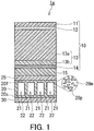
- a radio wave absorbing member 1a includes a radio wave absorber 10 and a support 20 having a sheet shape.
- the radio wave absorber 10 includes a resistive layer 12, a reflective layer 14, and a dielectric layer 13.
- the reflective layer 14 reflects a radio wave.
- the dielectric layer 13 is disposed between the resistive layer 12 and the reflective layer 14 in the thickness direction of the reflective layer 14.
- the radio wave absorber 10 is typically a ⁇ /4 radio wave absorber.
- the support 20 supports the radio wave absorber 10.
- the support 20 includes a matrix resin 20m and a flame retardant 20p. With the support 20 thus configured, the radio wave absorbing member 1a has desirable flame retardancy without including a flame retardant in the dielectric layer 13.
- the flame retardant 20p is unlikely to come into contact particularly with the resistive layer 12. Therefore, it is unlikely that the flame retardant 20p undesirably affects the resistive layer 12 by contact with the resistive layer 12, and the radio wave absorption performance of the radio wave absorber 10 is likely to be maintained for a long period of time.
- the support 20 is typically disposed at a position closer to the reflective layer 14 than to the resistive layer 12.
- the support 20 may be in contact with or apart from the reflective layer 14 in the thickness direction of the reflective layer 14.
- the support 20 includes, for example, a void 22 inside the support 20.
- an external impact on the radio wave absorbing member 1a can be absorbed by the support 20 including the void 22.
- the radio wave absorber 10 supported by the support 20 is likely to be protected from such an impact.
- the radio wave absorption performance of the radio wave absorber 10 is likely to be maintained for a long period of time.
- the support 20 includes, for example, a partition 21.
- the partition 21 partitions the inside of the support 20 into a plurality of the voids 22.
- the plurality of voids 22 are thus formed inside the support 20.
- the support 20 includes, for example, a first liner 20f forming one principal surface of the support 20 and a second liner 20s forming the other principal surface of the support 20.
- the partition 21 connects, for example, the first liner 20f and the second liner 20s.
- the partition 21 functions as a rib in the support 20.
- the plurality of partitions 21 extending in the same direction are aligned in a given direction.
- the support 20 may be produced by joining the first liner 20f, the second liner 20s, and the partition 21 or shaped integrally by extrusion.
- the void 22 may be formed in the form of a bubble.
- the support 20 is, for example, a foam.
- the bubble forming the void 22 may be an isolated bubble or a continuous bubble.
- the mass per unit area of the support 20 is, for example, 10 kg/m 2 or less. In this case, the weight of the radio wave absorbing member 1a is likely to be decreased.
- the mass per unit area of the support 20 may be 6 kg/m 2 or less or 3 kg/m 2 or less.
- the mass per unit area of the support 20 is, for example, 0.2 kg/m 2 or more. In this case, the support 20 is likely to have a desired rigidity.
- the mass per unit area of the support 12 may be 0.3 kg/m 2 or more or 0.5 kg/m 2 or more.
- the flexural modulus of the support 20 is, for example, 30 MPa or more. In this case, the radio wave absorbing member 1a is likely to have a desired flexural rigidity and the radio wave absorbing member 1a can be easily handled.
- the flexural modulus of the support 20 may be 50 MPa or more, 100 MPa or more, or 150 MPa or more.
- the flexural modulus of the support 20 is, for example, 5000 MPa or less. In this case, the radio wave absorbing member 1a can be easily handled.
- the flexural modulus of the support 20 may be 4000 MPa or less, 3000 MPa or less, or 1000 MPa or less.
- the matrix resin 20m is not limited to a particular resin, and can be any known resin.
- the matrix resin 20m there can be used, for example, a resin such as polyethylene, polypropylene, ethylene propylene block copolymer, polypropylene copolymer, polycarbonate, polyester, polystyrene, or acrylic resin.
- the matrix resin 20m may be a resin including a foaming agent and forming a foam.
- the flame retardant 20p is not limited to a particular flame retardant, and can be any known flame retardant.
- the flame retardant 20p may be made of an inorganic material or an organic material.
- PBDE polybrominated diphenyl ether
- TBBA tetrabromobisphenol A
- the phosphorus-containing flame retardant can be used an aromatic phosphoric acid ester such as triphenyl phosphate, a condensed aromatic phosphoric acid ester such as 1,3-phenylene bis(diphenyl phosphate), a halogen-containing phosphoric acid ester such as tris (dichloropropyl)phosphate, a halogen-condensed phosphoric acid ester such as 2,2-bis(chloromethyl)trimethylene bis(bis(2-chloroethyl)phosphate), a metal salt of phosphinic acid, an ammonium salt of polyphosphoric acid, or red phosphorus.
- the inorganic flame retardant there can be used a metal hydroxide such as magnesium hydroxide or aluminum hydroxide or a mineral such as antimony trioxide, antimony pentoxide, or talc.
- the flame retardant 20p is desirably in the form of particles including an inorganic material.
- the radio wave absorbing member 1a more reliably has desired flame retardancy.
- the support 20 is likely to have high flexural rigidity.
- the inorganic material can include the materials mentioned as examples of the above inorganic flame retardant.
- the content of the flame retardant 20p in the support 20 is not limited to a particular value.
- the content of the flame retardant 20p in the support 20 is, for example, 1 to 70 mass%.
- the radio wave absorbing member 1a more reliably has desired flame retardancy and the formability of the support 20 is likely to be good.
- the content of the flame retardant 20p in the support 20 may be, for example, 3 to 60 mass% or 5 to 50 mass%.
- the average burn rate of the radio wave absorbing member 1a is not limited to a particular value.
- the average burn rate of the radio wave absorbing member 1a can be determined by producing a specimen for a flammability test as in Federal Motor Vehicle Safety Standards (FMVSS) No. 302 using the radio wave absorbing member 1a, performing the flammability test several times according to FMVSS No. 302, and dividing the sum of the resulting burn rates obtained by the flammability test by the number of times the test was performed.
- FMVSS Federal Motor Vehicle Safety Standards
- the average burn rate of the radio wave absorbing member 1a is, for example, 15.0 mm/min or less, desirably 14.0 mm/min or less, more desirably 13.0 mm/min or less, even more desirably 12.0 mm/min or less, particularly desirably 11.0 mm/min or less, and extremely desirably 10.0 mm/min or less.
- the average burn rate of the radio wave absorbing member 1a is, for example, 1.0 mm/min or more, and may be 1.5 mm/min or more or 2.0 mm/min or more.
- the radio wave absorber 10 is designed so that incidence of a radio wave that is to be absorbed and has a wavelength ⁇ O on the radio wave absorber 1a will result in interference between a radio wave reflected by a surface of the resistive layer 12 (front surface reflection) and a radio wave reflected by the reflective layer 14 (back surface reflection).
- the wavelength ⁇ O of the radio wave to be absorbed is determined from the thickness t of the dielectric layer 13 and the relative permittivity ⁇ r of the dielectric layer 13, as shown in the following equation (1).
- sqrt( ⁇ r ) means a square root of the relative permittivity ⁇ r .
- ⁇ O 4 t ⁇ sqrt ⁇ r
- the resistive layer 12 is typically a layer adjusted so that an impedance expected on its front surface will be equal to a characteristic impedance of a plane wave.
- the resistive layer 12 can be formed of, for example, a metal, an alloy including a non-metal element, a metal oxide, an electrically conductive polymer, a carbon nanotube, a metal nanowire, or a metal mesh.
- the resistive layer 12 may include indium tin oxide.
- the resistive layer 12 includes indium tin oxide, the content of tin oxide in the indium tin oxide is, for example, 20 to 40 mass%.
- the resistive layer 12 can be formed by annealing treatment of indium tin oxide in a stable polycrystalline state. As a result, the radio wave absorption performance of the radio wave absorber 10 is likely to be maintained for a long period of time.
- the radio wave absorbing member 1a further includes, for example, a substrate 11.
- the resistive layer 12 is arranged, for example, on one principal surface of the substrate 11.
- the substrate 11, for example, serves as a support supporting the resistive layer 12.
- the material of the substrate 11 is, for example, polyethylene terephthalate (PET), polyethylene naphthalate (PEN), acrylic resin (PMMA), polycarbonate (PC), polyimide (PI), or cycloolefin polymer (COP).
- PET polyethylene terephthalate
- PEN polyethylene naphthalate
- acrylic resin PMMA
- PC polycarbonate
- PI polyimide
- COP cycloolefin polymer
- the material of the substrate 11 is desirably PET in terms of the balance between good heat resistance, the dimensional stability, and the manufacturing cost.
- the thickness of the substrate 11 is, for example, 10 to 150 ⁇ m and is desirably 15 to 100 ⁇ m.
- the substrate 11 has a low flexural rigidity, and occurrence of a crease in the substrate 11 or deformation of the substrate 11 at the time of formation of the resistive layer 12 can be reduced.
- the relative permittivity of the dielectric layer 13 is, for example, 2.0 to 20.0. In this case, the thickness of the dielectric layer 13 is easily adjusted and the radio wave absorption performance of the radio wave absorber 10 is easily adjusted.
- the relative permittivity of the dielectric layer 13 is, for example, a relative permittivity measured at 10 GHz by a cavity resonance method.
- the dielectric layer 13 is formed of, for example a given polymer.
- the dielectric layer 13 includes, for example, at least one polymer selected from the group consisting of ethylene vinyl acetate copolymer, vinyl chloride resin, urethane resin, acrylic resin, acrylic urethane resin, polyethylene, polypropylene, silicone, polyethylene terephthalate, polyethylene naphthalate, polycarbonate, polyimide, and cycloolefin polymer.
- the thickness of the dielectric layer 13 is easily adjusted and the manufacturing cost of the radio wave absorbing member 1a can be maintained at a low level.
- the dielectric layer 13 can be produced, for example, by hot-pressing a given resin composition.
- the dielectric layer 13 may be formed as a single layer or as a plurality of layers made of the same material or different materials.
- the relative permittivity of the dielectric layer 13 is determined, for example, as follows. The relative permittivity ⁇ i of each layer is measured (i is an integer of 1 to n). Next, the relative permittivity ⁇ i of each layer is multiplied by the proportion of the thickness ti of the layer in the total thickness T of the dielectric layer 13 to determine ⁇ i ⁇ (t i /T). The relative permittivity of the dielectric layer 13 can be determined by adding the ⁇ i ⁇ (ti/T) values of all layers.
- the dielectric layer 13 includes, for example, a first layer 13a and a second layer 13b.
- the first layer 13a is in contact with the resistive layer 12.
- the second layer 13b is disposed between the first layer 13a and the reflective layer 14.
- the dielectric layer 13 includes, for example, no flame retardant. In this case, it is less likely that the resistive layer 12 and the reflective layer 14 are undesirably affected by a flame retardant, and the radio wave absorption performance of the radio wave absorber 10 is likely to be maintained for a long period of time.
- the reflective layer 14 is not particularly limited as long as the reflective layer 14 can reflect a radio wave to be absorbed.
- the reflective layer 14 has, for example, a given electrical conductivity.
- the reflective layer 14 may include, for example, at least one selected from the group consisting of aluminum, copper, iron, aluminum alloys, copper alloys, and iron alloys. In this case, the thickness of the reflective layer 14 is likely to be reduced.
- the reflective layer 14 may be a metal oxide such as indium tin oxide as long as the reflective layer 14 has the given electrical conductivity.
- the thickness of the reflective layer 14 is not limited to a particular value.
- the thickness of the reflective layer 14 is, for example, 20 nm to 100 ⁇ m and is desirably 50 nm to 50 ⁇ m.
- the radio wave absorbing member 1a further includes, for example, a substrate 15.
- the reflective layer 14 is arranged, for example, on one principal surface of the substrate 15.
- the substrate 15, for example, serves as a support supporting the reflective layer 14.
- the material of the substrate 15 is, for example, polyethylene terephthalate (PET), polyethylene naphthalate (PEN), acrylic resin (PMMA), polycarbonate (PC), polyimide (PI), or cycloolefin polymer (COP).
- PET polyethylene terephthalate
- PEN polyethylene naphthalate
- acrylic resin PMMA
- PC polycarbonate
- PI polyimide
- COP cycloolefin polymer
- the material of the substrate 15 is desirably PET in terms of the balance between good heat resistance, the dimensional stability, and the manufacturing cost.
- the radio wave absorbing member 1a further includes, for example, an adhesive layer 25 and an adhesive layer 30.
- the adhesive layer 25 is disposed between the radio wave absorber 10 and the support 20.
- the adhesive layer 25 achieves integration of the support 20 and the radio wave absorber 10 to give the radio wave absorbing member 1a.
- the adhesive layer 30 is arranged on a principal surface of the support 20.
- the principal surface is remote from the radio wave absorber 10.
- the radio wave absorbing member 1a can be disposed at a given position by pressing the adhesive layer 30 against a given plane.
- the adhesive layer 25 and the adhesive layer 30 each include, for example, a rubber adhesive, an acrylic adhesive, a silicone adhesive, or a urethane adhesive.
- the radio wave absorbing member 1a may further include a release liner (not illustrated).
- the release liner covers the adhesive layer 30.
- the release liner can maintain the adhesive strength of the adhesive layer 30 while covering the adhesive layer 30, and the release liner can be easily peeled off from the adhesive layer 30.
- the release liner is, for example, a film made of a polyester resin such as PET. The adhesive layer 30 is exposed by peeling off the release liner, so that the radio wave absorbing member 1a is able to stick to a given plane.
- the radio wave absorbing member 1a can be modified in various respects.
- the reflective layer 14 may be arranged on one principal surface of the support 20.
- the substrate 15 and the adhesive layer 25 can be omitted, and the surface of the dielectric layer 13, the surface being in contact with the reflective layer 14, can be formed as an adhesive surface.
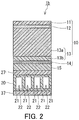
- the radio wave absorbing member 1a may be modified to a radio wave absorbing member 1b shown in FIG. 2 or a radio wave absorbing member 1c shown in FIG. 3 .
- the radio wave absorbing members 1b and 1c are configured in the same manner as the radio wave absorbing member 1a unless otherwise described.
- the components of the radio wave absorbing members 1b and 1c that are the same as or correspond to the components of the radio wave absorbing member 1a are denoted by the same reference characters, and detailed descriptions of such components are omitted.
- the description given for the radio wave absorbing member 1a is applicable to the radio wave absorbing members 1b and 1c unless there is a technical inconsistency.
- the radio wave absorbing member 1b further includes, a flame-retardant layer 27.
- the flame-retardant layer 27 is disposed between the support 20 and the radio wave absorber 20 and includes a flame retardant. Having such a configuration, the radio wave absorbing member 1b is likely to have higher flame retardancy.
- the flame retardant included in the flame-retardant layer 27 may be the same flame retardant as the flame retardant 20p included in the support 20 or may be a different flame retardant therefrom.
- the flame-retardant layer 27 may further include, for example, an adhesive. In this case, the flame-retardant layer 27 achieves integration of the support 20 and the radio wave absorber 10.
- the radio wave absorbing member 1b further includes a flame-retardant layer 37.
- the flame-retardant layer 37 is arranged on a principal surface of the support 20. The principal surface is remote from the radio wave absorber 10 and includes a flame retardant. Having such a configuration, the radio wave absorbing member 1b is likely to have higher flame retardancy.
- the flame retardant included in the flame-retardant layer 37 may be the same flame retardant as the flame retardant 20p included in the support 20 or may be a different flame retardant therefrom.
- the flame-retardant layer 37 may include, for example, an adhesive. This makes it possible to dispose the radio wave absorbing member 1b at a given position by pressing the radio wave absorbing member 1b against a given plane.
- the radio wave absorber 10 includes a plurality of radio wave absorbing portions.
- the radio wave absorber 10 includes, for example, a first radio wave absorbing portion 10a and a second radio wave absorbing portion 10b.
- the first radio wave absorbing portion 10a has the largest amount of reflection and absorption of a radio wave having a given frequency, as measured according to Japanese Industrial Standards (JIS) R 1679:2007, at a first incident angle in the incident angle range of 0° to 80°.
- JIS Japanese Industrial Standards
- the first radio wave absorbing portion 10a has the largest amount of reflection and absorption of a radio wave having a given frequency, as measured according to JIS R 1679:2007, at a second incident angle in the incident angle range of 0° to 80°.
- the second incident angle is different from the first incident angle, or the polarized wave type of a radio wave incident at the second incident angle is different from the polarized wave type of a radio wave incident at the first incident angle.
- the term "amount of reflection and absorption” is synonymous with, for example, the absolute value of a return loss S (dB) defined by the following equation (2).
- P 0 is received power (W/m 2 ) obtained from reflection by a metal plate
- P i is received power (W/m 2 ) obtained from reflection by a sample.
- the amount of reflection and absorption corresponds to the absolute value of the amount of reflection as in JIS R 1679:2007.
- S 10 log P i / P 0
- the first radio wave absorbing portion 10a is composed of, for example, a first resistive layer 12a, a first dielectric layer 13f, a common dielectric layer 13c, and the reflective layer 14.
- the first radio wave absorbing portion 10a further includes, for example, a first substrate 11a.
- the second radio wave absorbing portion 10b is composed of, for example, a second resistive layer 12b, a second dielectric layer 13s, the common dielectric layer 13c, and the reflective layer 14.
- the second radio wave absorbing portion 10b further includes, for example, a second substrate 11b.
- the radio wave absorbing member 1c is likely to exhibit the desired absorption performance with respect to a radio wave incident at an incident angle in a wide range or a variety of polarized waves.
- the first and second radio wave absorbing portions 10a and 10b are disposed over the same support 20.
- the first and second radio wave absorbing portions 10a and 10b may be disposed on different supports 20.
- the first and second radio wave absorbing portions 10a and 10b are disposed, for example, over the same adhesive layer 25.
- the first and second radio wave absorbing portions 10a and 10b may be disposed on different adhesive layers 25.
- the first and second radio wave absorbing portions 10a and 10b are disposed, for example, over the same adhesive layer 30.
- the first and second radio wave absorbing portions 10a and 10b may be disposed on different adhesive layers 30.
- the reflective layer 14 shared by the first and second radio wave absorbing portions 10a and 10b.
- the reflective layer 14 may be arranged in each of the first and second radio wave absorbing portions 10a and 10b.
- the applications of the radio wave absorbing members 1a, 1b, and 1c are not particularly limited.
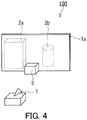
- an inspection apparatus 100 shown in FIG. 4 can be provided with the use of the radio wave absorbing member 1a.
- the inspection apparatus 100 includes radio wave reflectors 2a and 2b and the radio wave absorbing member 1a.
- the radio wave absorbing member 1a is disposed so as to absorb a radio wave travelling toward the radio wave reflectors 2a and 2b.
- the inspection apparatus 100 further includes, for example, a target 5.
- a device to be inspected is disposed so as to face the target 5.
- the device to be inspected includes, for example, an antenna 7 and uses a given radio wave for sensing. A radio wave emitted from the antenna 7 of the device to be inspected is reflected by the target 5, and the reflected radio wave is led to the antenna 7 of the device to be inspected. Whether the device to be inspected can appropriately detect the target 5 can be inspected in this manner.
- the radio wave reflectors 2a and 2b are, for example, a housing of a measuring instrument needed for inspection using the inspection apparatus 100 or a jig. But for the radio wave absorbing member 1a in the inspection apparatus 100, the radio wave emitted from the antenna 7 would be reflected by the radio wave reflectors 2a and 2b and then led back to the antenna 7. The radio waves reflected by the radio wave reflectors 2a and 2b are, however, unnecessary radio waves, which need to be excluded for accurate inspection. With the radio wave absorbing member 1a disposed as shown in FIG. 4 , the radio wave emitted from the device to be inspected can be prevented from being reflected by the radio wave reflectors 2a and 2b and being led to the device to be inspected. Therefore, the inspection apparatus 100 can appropriately inspect the device to be inspected.
- the radio wave absorbing member 1a is, for example, disposed so that a radio wave emitted from the antenna 7 can be incident perpendicularly on the radio wave absorbing member 1a.
- the radio wave absorbing member 1a is disposed, for example, behind the target 5.
- the radio wave reflectors 2a and 2b can be disposed on a lateral side of a space between the antenna 7 and the target 5. Therefore, the radio wave absorbing member 1a may be disposed on a lateral side of and along a space between the antenna 7 and the target 5.
- the radio wave absorbing member 1b or the radio wave absorbing member 1c may be disposed instead of the radio wave absorbing member 1a.
- a radio wave absorbing structure 200 shown in FIG. 5 can be provided with the use of the radio wave absorbing member 1.
- the radio wave absorbing structure 200 includes the plurality of radio wave absorbing members 1a.
- the plurality of radio wave absorbing members 1a are disposed apart from each other.
- the plurality of radio wave absorbing members 1a are disposed apart from each other in the radio wave absorbing structure 200, the arrangement of the radio wave absorbing members 1a is unlikely to be affected by a dimensional difference between the adjacent radio wave absorbing members 1a. Therefore, the plurality of radio wave absorbing members 1a are appropriately disposed throughout the radio wave absorbing structure 200.
- the radio wave absorbing member 1a may be composed of one piece or may be composed of a plurality of pieces connected to each other.
- the plurality of radio wave absorbing members 1b or the plurality of radio wave absorbing members 1c instead of the radio wave absorbing members 1a, may be disposed apart from each other.
- a resistive layer having a sheet resistance of 370 ⁇ / ⁇ was formed on a 23- ⁇ m-thick PET film by sputtering using ITO as a target material.
- a resistive layer-including film was obtained in this manner.
- An acrylic resin layer was obtained by shaping an acrylic resin having a relative permittivity of 2.6 to a thickness of 560 ⁇ m.
- the resistive layer-including film was stacked on the acrylic resin layer so that the resistive layer of the resistive layer-including film would be in contact with the acrylic resin layer.
- the resistive layer-including film was adhered to the acrylic resin layer without using an adhesive.
- An electrical conductor-including film in which a 7- ⁇ m-thick aluminum foil is sandwiched between a 25- ⁇ m-thick PET film and a 9- ⁇ m-thick PET film and the aluminum foil and the PET films are laminated was prepared.
- the electrical conductor-including film and the laminate consisting of the resistive layer-including film and the acrylic resin layer were stacked so that the electrical conductor-including film would be in contact with the acrylic resin layer of the laminate.
- a radio wave absorber was obtained in this manner.
- a commercially-available resin corrugated cardboard (manufactured by SUMIKA PLASTECH Co., Ltd., product name: WT09300) was prepared as a support.
- the support included talc serving as a flame retardant.
- the support had a thickness of 9 mm.
- a double-faced adhesive tape (manufactured by Nitto Denko Corporation, product name: No. 5635) was disposed between the electrical conductor-including film of the radio wave absorber and the corrugated cardboard, and then the radio wave absorber was stuck to the corrugated cardboard.
- the double-faced adhesive tape had a thickness of 0.15 mm and included no flame retardant.
- a radio wave absorbing member according to Example 1 was obtained in this manner.
- a radio wave absorbing member according to Example 2 was obtained in the same manner as in Example 1, except that a double-faced adhesive tape TR-5912F including a flame retardant and manufactured by Nitto Denko Corporation was used instead of the double-faced adhesive tape No. 5635 manufactured by Nitto Denko Corporation and that two pieces of the double-faced adhesive tape TR-5912F were stacked and disposed between the electrical conductor-including film of the radio wave absorber and the corrugated cardboard. Each piece of the double-faced adhesive tape had a thickness of 0.125 mm.
- a radio wave absorber as described above and not stuck to a corrugated cardboard was used as a radio wave absorbing member according to Comparative Example 1.
- a radio wave absorbing member according to Comparative Example 2 was obtained in the same manner as in Example 1, except that an acrylic resin sheet was used as a support instead of the resin corrugated cardboard.
- the acrylic resin sheet had a thickness of 2.0 mm.
- a radio wave absorbing member according to Comparative Example 3 was obtained in the same manner as in Example 1, except that a hollow polycarbonate board KTP4534W-1, which is a resin corrugated cardboard manufactured by AiTec and including no flame retardant, was used as a support.
- the corrugated cardboard had a thickness of 4.00 mm.
- the radio wave absorbing member according to Example 1 and the radio wave absorbing members according to Comparative Examples 1 and 2 were subjected to a ball drop test.
- a metal ball having a weight of 500 g and a diameter of 50 mm was used in the ball drop test.
- the metal ball was allowed to fall freely seven times from a height of 300 mm to each radio wave absorbing member cut into A4 size.
- a visual comparison of damage caused by the falling metal ball was made between the radio wave absorbing member according to Example 1 and the radio wave absorbing member according to Comparative Example 1. The comparison revealed that the damage on the radio wave absorbing member according to Comparative Example 1 was more severe than that on the radio wave absorbing member according to Example 1.
- the amount of radio wave reflection was measured according to JIS R 1679:2007 for the radio wave absorbing members according to Example 1 and Comparative Example 2 using a 76-GHz millimeter wave perpendicularly incident thereon.
- the average difference ⁇ ave in amounts of radio wave reflection was determined by subtracting the average of the amounts of radio wave reflection before the ball drop test from the average of the amounts of radio wave reflection after the ball drop test.
- Table 1 shows the results. It is indicated that impact made by a falling ball is easily absorbed by the corrugated cardboard of the radio wave absorbing member according to Example 1 and the amount of radio wave reflection by the radio wave absorbing member according to Example 1 is maintained easily regardless of a fall of the ball.
- a specimen for a flammability test as in FMVSS No. 302 was produced from each of the radio wave absorbing members according to Example 1, Example 2, and Comparative Example 3.
- a marked line A and a marked line B were drawn respectively at positions 38 mm and 292 mm away from one end in the longitudinal direction of the specimen.
- the one end in the longitudinal direction of the specimen was exposed to a 38-mm-long flame for 15 seconds, and the burn rate in the 254-mm-long zone between the marked line A and marked line B was determined according to FMVSS No. 302.
- the radio wave absorbing members according to Example 1, Example 2, and Comparative Example 3 were each subjected to the flammability test several times.
- Example 2 The sum of the burn rates obtained by the flammability test was divided by the number of times the test was performed to determine the average burn rate of each of the radio wave absorbing members according to Example 1, Example 2, and Comparative Example 3.
- Table 2 shows the results. As shown in Table 2, the average burn rates of the radio wave absorbing members according to Example 1 and Example 2 were lower than the average burn rate of the radio wave absorbing member according to Comparative Example 3. This indicates that in terms of increasing the flame retardancy of a radio wave absorbing member, inclusion of a flame retardant in a support is advantageous. Additionally, the average burn rate of the radio wave absorbing member according to Example 2 was lower than the average burn rate of the radio wave absorbing member according to Example 1.
Landscapes
- Chemical & Material Sciences (AREA)
- Electromagnetism (AREA)
- Engineering & Computer Science (AREA)
- Microelectronics & Electronic Packaging (AREA)
- Physics & Mathematics (AREA)
- Chemical Kinetics & Catalysis (AREA)
- Health & Medical Sciences (AREA)
- Medicinal Chemistry (AREA)
- Polymers & Plastics (AREA)
- Organic Chemistry (AREA)
- Shielding Devices Or Components To Electric Or Magnetic Fields (AREA)
- Laminated Bodies (AREA)
- Aerials With Secondary Devices (AREA)
Abstract
Description
- The present invention relates to a radio wave absorbing member, a radio wave absorbing structure, and an inspection apparatus.
- λ/4 radio wave absorbers have been known. λ/4 radio wave absorbers show a higher return loss than that of other radio wave absorbers such as magnetic loss-type radio wave absorbers. Therefore, it is conceivable that in order to absorb unnecessary radio waves, λ/4 radio wave absorbers are used, for example, in millimeter-wave radar systems to be mounted on vehicles or in facilities where millimeter-wave radar systems are inspected.
- In a known form of λ/4 radio wave absorbers, a resistive layer, a dielectric layer, and an electrically conductive layer are laminated in this order. The dielectric layer, which is commonly made of a resin material, is flammable. Therefore, it is advantageous that the flame retardancy of the λ/4 radio wave absorbers is improved in the case where the λ/4 radio wave absorbers are used, as stated above, in devices to be mounted on vehicles or in facilities where such devices are inspected.
- For example,
Patent Literature 1 describes provision of a glass layer on the surface of a λ/4 radio wave absorber. This allows protection of the radio wave absorber from burning due to, for example, an undesired fire. - Patent Literature 1:
JP 2006-086446 A - In the case of the technique described in
Patent Literature 1, the flexibility of the radio wave absorber must be very low because of the glass layer disposed on the surface of the radio wave absorber. Accordingly, the radio wave absorber can be installed only in limited locations. Moreover, as the glass layer is disposed, there are concerns that the total weight of the radio wave absorber may increase and impact on the radio wave absorber may break the glass layer to decrease the radio wave absorption performance. - Then, it is conceivable that in order to increase the flame retardancy of a λ/4 radio wave absorber, a flame retardant is included in its dielectric layer. The dielectric layer is in contact with a resistive layer made of a material such as a metal oxide and an electrically conductive layer formed of an electrical conductivity material such as a metal. Thus, inclusion of a flame retardant in the dielectric layer may cause an undesirable effect on the resistive layer or the electrically conductive layer. For example, the resistive layer or the electrically conductive layer may be detached or the properties of the resistive layer may change. Such effects are disadvantageous in terms of maintaining the radio wave absorption performance of the λ/4 radio wave absorber for a long period of time.
- In view of such circumstances, the present invention provides a radio wave absorbing member that is advantageous in terms of maintaining the radio wave absorption performance of a λ/4 radio wave absorber for a long period of time and increasing the flame retardancy. The present invention also provides a radio wave absorbing structure including such a radio wave absorbing member and an inspection apparatus including such a radio wave absorbing member.
- The present invention provides a radio wave absorbing member including:
- a radio wave absorber including a resistive layer, a reflective layer that reflects a radio wave, and a dielectric layer disposed between the resistive layer and the reflective layer in the thickness direction of the reflective layer; and
- a support having a sheet shape and supporting the radio wave absorber, wherein
- the support includes a matrix resin and a flame retardant.
- The present invention also provides a radio wave absorbing structure including:
- a plurality of the above radio wave absorbing members, wherein
- the plurality of radio wave absorbing members are disposed apart from each other.
- The present invention also provides an inspection apparatus including:
- a radio wave reflector; and
- the above radio wave absorbing member, wherein
- the radio wave absorbing member is disposed so as to absorb a radio wave travelling toward the radio wave reflector.
- The above radio wave absorbing member is advantageous in terms of maintaining the radio wave absorption performance of a λ/4 radio wave absorber for a long period of time and increasing the flame retardancy.
-
-
FIG. 1 is a cross-sectional view showing an example of a radio wave absorbing member according to the present invention. -
FIG. 2 is a cross-sectional view showing another example of the radio wave absorbing member according to the present invention. -
FIG. 3 is a cross-sectional view showing yet another example of the radio wave absorbing member according to the present invention. -
FIG. 4 is a perspective view showing an example of an inspection apparatus according to the present invention. -
FIG. 5 is a perspective view showing an example of a radio wave absorbing structure according to the present invention. - Hereinafter, embodiments of the present invention will be described with reference to the drawings. The present invention is not limited to the following embodiments.
- As shown in
FIG. 1 , a radiowave absorbing member 1a includes a radio wave absorber 10 and asupport 20 having a sheet shape. The radio wave absorber 10 includes aresistive layer 12, areflective layer 14, and adielectric layer 13. Thereflective layer 14 reflects a radio wave. Thedielectric layer 13 is disposed between theresistive layer 12 and thereflective layer 14 in the thickness direction of thereflective layer 14. The radio wave absorber 10 is typically a λ/4 radio wave absorber. Thesupport 20 supports the radio wave absorber 10. Thesupport 20 includes amatrix resin 20m and a flame retardant 20p. With thesupport 20 thus configured, the radiowave absorbing member 1a has desirable flame retardancy without including a flame retardant in thedielectric layer 13. Included in thesupport 20, the flame retardant 20p is unlikely to come into contact particularly with theresistive layer 12. Therefore, it is unlikely that the flame retardant 20p undesirably affects theresistive layer 12 by contact with theresistive layer 12, and the radio wave absorption performance of the radio wave absorber 10 is likely to be maintained for a long period of time. - The
support 20 is typically disposed at a position closer to thereflective layer 14 than to theresistive layer 12. Thesupport 20 may be in contact with or apart from thereflective layer 14 in the thickness direction of thereflective layer 14. - As shown in
FIG. 1 , thesupport 20 includes, for example, avoid 22 inside thesupport 20. With such a configuration, an external impact on the radiowave absorbing member 1a can be absorbed by thesupport 20 including thevoid 22. Hence, the radio wave absorber 10 supported by thesupport 20 is likely to be protected from such an impact. As a result, the radio wave absorption performance of the radio wave absorber 10 is likely to be maintained for a long period of time. - The
support 20 includes, for example, apartition 21. Thepartition 21 partitions the inside of thesupport 20 into a plurality of thevoids 22. The plurality ofvoids 22 are thus formed inside thesupport 20. - The
support 20 includes, for example, a first liner 20f forming one principal surface of thesupport 20 and a second liner 20s forming the other principal surface of thesupport 20. Thepartition 21 connects, for example, the first liner 20f and the second liner 20s. In other words, thepartition 21 functions as a rib in thesupport 20. For example, in thesupport 20, the plurality ofpartitions 21 extending in the same direction are aligned in a given direction. Thesupport 20 may be produced by joining the first liner 20f, the second liner 20s, and thepartition 21 or shaped integrally by extrusion. - In the
support 20, the void 22 may be formed in the form of a bubble. In this case, thesupport 20 is, for example, a foam. The bubble forming the void 22 may be an isolated bubble or a continuous bubble. - The mass per unit area of the
support 20 is, for example, 10 kg/m2 or less. In this case, the weight of the radiowave absorbing member 1a is likely to be decreased. The mass per unit area of thesupport 20 may be 6 kg/m2 or less or 3 kg/m2 or less. The mass per unit area of thesupport 20 is, for example, 0.2 kg/m2 or more. In this case, thesupport 20 is likely to have a desired rigidity. The mass per unit area of thesupport 12 may be 0.3 kg/m2 or more or 0.5 kg/m2 or more. - The flexural modulus of the
support 20 is, for example, 30 MPa or more. In this case, the radiowave absorbing member 1a is likely to have a desired flexural rigidity and the radiowave absorbing member 1a can be easily handled. The flexural modulus of thesupport 20 may be 50 MPa or more, 100 MPa or more, or 150 MPa or more. The flexural modulus of thesupport 20 is, for example, 5000 MPa or less. In this case, the radiowave absorbing member 1a can be easily handled. The flexural modulus of thesupport 20 may be 4000 MPa or less, 3000 MPa or less, or 1000 MPa or less. - The flexural modulus of the
support 20 can be determined, for example, as follows. A rectangle having a width of 50 mm and a length of 150 mm is cut out from thesupport 20 to produce a specimen. The specimen is subjected to a bending test using a bending tester under the following test conditions. The flexural modulus can be calculated, as defined in Japanese Industrial Standards (JIS) Z 7171, based on the amount of strain and the flexural stress after calculation of deflections s1 and s2 respectively corresponding to flexural strains ε1 = 0.0005 and ε2 = 0.0025.
Test condition: three-point bending; span between supports: 100 mm; test speed: 10 mm/min; environmental temperature: room temperature (23°C) - The
matrix resin 20m is not limited to a particular resin, and can be any known resin. As thematrix resin 20m there can be used, for example, a resin such as polyethylene, polypropylene, ethylene propylene block copolymer, polypropylene copolymer, polycarbonate, polyester, polystyrene, or acrylic resin. Thematrix resin 20m may be a resin including a foaming agent and forming a foam. - The
flame retardant 20p is not limited to a particular flame retardant, and can be any known flame retardant. Theflame retardant 20p may be made of an inorganic material or an organic material. As theflame retardant 20p there can be used, for example, a bromine-containing flame retardant, a phosphorus-containing flame retardant, or an inorganic flame retardant. As the bromine-containing flame retardant there can be used, for example, polybrominated diphenyl ether (PBDE), tetrabromobisphenol A (TBBA), or brominated polystyrene. As the phosphorus-containing flame retardant can be used an aromatic phosphoric acid ester such as triphenyl phosphate, a condensed aromatic phosphoric acid ester such as 1,3-phenylene bis(diphenyl phosphate), a halogen-containing phosphoric acid ester such as tris (dichloropropyl)phosphate, a halogen-condensed phosphoric acid ester such as 2,2-bis(chloromethyl)trimethylene bis(bis(2-chloroethyl)phosphate), a metal salt of phosphinic acid, an ammonium salt of polyphosphoric acid, or red phosphorus. As the inorganic flame retardant there can be used a metal hydroxide such as magnesium hydroxide or aluminum hydroxide or a mineral such as antimony trioxide, antimony pentoxide, or talc. - The
flame retardant 20p is desirably in the form of particles including an inorganic material. In this case, the radiowave absorbing member 1a more reliably has desired flame retardancy. Moreover, when theflame retardant 20p is made of an inorganic material, thesupport 20 is likely to have high flexural rigidity. Examples of the inorganic material can include the materials mentioned as examples of the above inorganic flame retardant. - The content of the
flame retardant 20p in thesupport 20 is not limited to a particular value. The content of theflame retardant 20p in thesupport 20 is, for example, 1 to 70 mass%. In this case, the radiowave absorbing member 1a more reliably has desired flame retardancy and the formability of thesupport 20 is likely to be good. The content of theflame retardant 20p in thesupport 20 may be, for example, 3 to 60 mass% or 5 to 50 mass%. - The average burn rate of the radio
wave absorbing member 1a is not limited to a particular value. The average burn rate of the radiowave absorbing member 1a can be determined by producing a specimen for a flammability test as in Federal Motor Vehicle Safety Standards (FMVSS) No. 302 using the radiowave absorbing member 1a, performing the flammability test several times according to FMVSS No. 302, and dividing the sum of the resulting burn rates obtained by the flammability test by the number of times the test was performed. The average burn rate of the radiowave absorbing member 1a is, for example, 15.0 mm/min or less, desirably 14.0 mm/min or less, more desirably 13.0 mm/min or less, even more desirably 12.0 mm/min or less, particularly desirably 11.0 mm/min or less, and extremely desirably 10.0 mm/min or less. The average burn rate of the radiowave absorbing member 1a is, for example, 1.0 mm/min or more, and may be 1.5 mm/min or more or 2.0 mm/min or more. - The
radio wave absorber 10 is designed so that incidence of a radio wave that is to be absorbed and has a wavelength λO on theradio wave absorber 1a will result in interference between a radio wave reflected by a surface of the resistive layer 12 (front surface reflection) and a radio wave reflected by the reflective layer 14 (back surface reflection). In theradio wave absorber 10, the wavelength λO of the radio wave to be absorbed is determined from the thickness t of thedielectric layer 13 and the relative permittivity εr of thedielectric layer 13, as shown in the following equation (1). In the equation (1), sqrt(εr) means a square root of the relative permittivity εr.
- The
resistive layer 12 is typically a layer adjusted so that an impedance expected on its front surface will be equal to a characteristic impedance of a plane wave. Theresistive layer 12 can be formed of, for example, a metal, an alloy including a non-metal element, a metal oxide, an electrically conductive polymer, a carbon nanotube, a metal nanowire, or a metal mesh. Theresistive layer 12 may include indium tin oxide. When theresistive layer 12 includes indium tin oxide, the content of tin oxide in the indium tin oxide is, for example, 20 to 40 mass%. In this case, theresistive layer 12 can be formed by annealing treatment of indium tin oxide in a stable polycrystalline state. As a result, the radio wave absorption performance of theradio wave absorber 10 is likely to be maintained for a long period of time. - As shown in
FIG. 1 , the radiowave absorbing member 1a further includes, for example, asubstrate 11. Theresistive layer 12 is arranged, for example, on one principal surface of thesubstrate 11. Thesubstrate 11, for example, serves as a support supporting theresistive layer 12. The material of thesubstrate 11 is, for example, polyethylene terephthalate (PET), polyethylene naphthalate (PEN), acrylic resin (PMMA), polycarbonate (PC), polyimide (PI), or cycloolefin polymer (COP). Among these, the material of thesubstrate 11 is desirably PET in terms of the balance between good heat resistance, the dimensional stability, and the manufacturing cost. - The thickness of the
substrate 11 is, for example, 10 to 150 µm and is desirably 15 to 100 µm. In this case, thesubstrate 11 has a low flexural rigidity, and occurrence of a crease in thesubstrate 11 or deformation of thesubstrate 11 at the time of formation of theresistive layer 12 can be reduced. - The relative permittivity of the
dielectric layer 13 is, for example, 2.0 to 20.0. In this case, the thickness of thedielectric layer 13 is easily adjusted and the radio wave absorption performance of theradio wave absorber 10 is easily adjusted. The relative permittivity of thedielectric layer 13 is, for example, a relative permittivity measured at 10 GHz by a cavity resonance method. - The
dielectric layer 13 is formed of, for example a given polymer. Thedielectric layer 13 includes, for example, at least one polymer selected from the group consisting of ethylene vinyl acetate copolymer, vinyl chloride resin, urethane resin, acrylic resin, acrylic urethane resin, polyethylene, polypropylene, silicone, polyethylene terephthalate, polyethylene naphthalate, polycarbonate, polyimide, and cycloolefin polymer. In this case, the thickness of thedielectric layer 13 is easily adjusted and the manufacturing cost of the radiowave absorbing member 1a can be maintained at a low level. Thedielectric layer 13 can be produced, for example, by hot-pressing a given resin composition. - The
dielectric layer 13 may be formed as a single layer or as a plurality of layers made of the same material or different materials. When thedielectric layer 13 includes n layers (n is an integer of 2 or greater), the relative permittivity of thedielectric layer 13 is determined, for example, as follows. The relative permittivity εi of each layer is measured (i is an integer of 1 to n). Next, the relative permittivity εi of each layer is multiplied by the proportion of the thickness ti of the layer in the total thickness T of thedielectric layer 13 to determine εi × (ti/T). The relative permittivity of thedielectric layer 13 can be determined by adding the εi × (ti/T) values of all layers. - As shown in
FIG. 1 , thedielectric layer 13 includes, for example, afirst layer 13a and asecond layer 13b. Thefirst layer 13a is in contact with theresistive layer 12. Thesecond layer 13b is disposed between thefirst layer 13a and thereflective layer 14. - The
dielectric layer 13 includes, for example, no flame retardant. In this case, it is less likely that theresistive layer 12 and thereflective layer 14 are undesirably affected by a flame retardant, and the radio wave absorption performance of theradio wave absorber 10 is likely to be maintained for a long period of time. - The
reflective layer 14 is not particularly limited as long as thereflective layer 14 can reflect a radio wave to be absorbed. Thereflective layer 14 has, for example, a given electrical conductivity. Thereflective layer 14 may include, for example, at least one selected from the group consisting of aluminum, copper, iron, aluminum alloys, copper alloys, and iron alloys. In this case, the thickness of thereflective layer 14 is likely to be reduced. Thereflective layer 14 may be a metal oxide such as indium tin oxide as long as thereflective layer 14 has the given electrical conductivity. - The thickness of the
reflective layer 14 is not limited to a particular value. The thickness of thereflective layer 14 is, for example, 20 nm to 100 µm and is desirably 50 nm to 50 µm. - As shown in
FIG. 1 , the radiowave absorbing member 1a further includes, for example, asubstrate 15. Thereflective layer 14 is arranged, for example, on one principal surface of thesubstrate 15. Thesubstrate 15, for example, serves as a support supporting thereflective layer 14. The material of thesubstrate 15 is, for example, polyethylene terephthalate (PET), polyethylene naphthalate (PEN), acrylic resin (PMMA), polycarbonate (PC), polyimide (PI), or cycloolefin polymer (COP). Among these, the material of thesubstrate 15 is desirably PET in terms of the balance between good heat resistance, the dimensional stability, and the manufacturing cost. - As shown in
FIG. 1 , the radiowave absorbing member 1a further includes, for example, anadhesive layer 25 and anadhesive layer 30. Theadhesive layer 25 is disposed between theradio wave absorber 10 and thesupport 20. For example, theadhesive layer 25 achieves integration of thesupport 20 and theradio wave absorber 10 to give the radiowave absorbing member 1a. - The
adhesive layer 30 is arranged on a principal surface of thesupport 20. The principal surface is remote from theradio wave absorber 10. For example, the radiowave absorbing member 1a can be disposed at a given position by pressing theadhesive layer 30 against a given plane. - The
adhesive layer 25 and theadhesive layer 30 each include, for example, a rubber adhesive, an acrylic adhesive, a silicone adhesive, or a urethane adhesive. The radiowave absorbing member 1a may further include a release liner (not illustrated). In this case, the release liner covers theadhesive layer 30. Typically, the release liner can maintain the adhesive strength of theadhesive layer 30 while covering theadhesive layer 30, and the release liner can be easily peeled off from theadhesive layer 30. The release liner is, for example, a film made of a polyester resin such as PET. Theadhesive layer 30 is exposed by peeling off the release liner, so that the radiowave absorbing member 1a is able to stick to a given plane. - The radio
wave absorbing member 1a can be modified in various respects. For example, thereflective layer 14 may be arranged on one principal surface of thesupport 20. In this case, thesubstrate 15 and theadhesive layer 25 can be omitted, and the surface of thedielectric layer 13, the surface being in contact with thereflective layer 14, can be formed as an adhesive surface. - The radio
wave absorbing member 1a may be modified to a radiowave absorbing member 1b shown inFIG. 2 or a radiowave absorbing member 1c shown inFIG. 3 . The radiowave absorbing members wave absorbing member 1a unless otherwise described. The components of the radiowave absorbing members wave absorbing member 1a are denoted by the same reference characters, and detailed descriptions of such components are omitted. The description given for the radiowave absorbing member 1a is applicable to the radiowave absorbing members - As shown in
FIG. 2 , the radiowave absorbing member 1b further includes, a flame-retardant layer 27. The flame-retardant layer 27 is disposed between thesupport 20 and theradio wave absorber 20 and includes a flame retardant. Having such a configuration, the radiowave absorbing member 1b is likely to have higher flame retardancy. - The flame retardant included in the flame-
retardant layer 27 may be the same flame retardant as theflame retardant 20p included in thesupport 20 or may be a different flame retardant therefrom. - The flame-
retardant layer 27 may further include, for example, an adhesive. In this case, the flame-retardant layer 27 achieves integration of thesupport 20 and theradio wave absorber 10. - As shown in
FIG. 2 , the radiowave absorbing member 1b further includes a flame-retardant layer 37. The flame-retardant layer 37 is arranged on a principal surface of thesupport 20. The principal surface is remote from theradio wave absorber 10 and includes a flame retardant. Having such a configuration, the radiowave absorbing member 1b is likely to have higher flame retardancy. The flame retardant included in the flame-retardant layer 37 may be the same flame retardant as theflame retardant 20p included in thesupport 20 or may be a different flame retardant therefrom. The flame-retardant layer 37 may include, for example, an adhesive. This makes it possible to dispose the radiowave absorbing member 1b at a given position by pressing the radiowave absorbing member 1b against a given plane. - In the radio
wave absorbing member 1c, theradio wave absorber 10 includes a plurality of radio wave absorbing portions. Theradio wave absorber 10 includes, for example, a first radiowave absorbing portion 10a and a second radiowave absorbing portion 10b. The first radiowave absorbing portion 10a has the largest amount of reflection and absorption of a radio wave having a given frequency, as measured according to Japanese Industrial Standards (JIS) R 1679:2007, at a first incident angle in the incident angle range of 0° to 80°. The first radiowave absorbing portion 10a has the largest amount of reflection and absorption of a radio wave having a given frequency, as measured according to JIS R 1679:2007, at a second incident angle in the incident angle range of 0° to 80°. In theradio wave absorber 10, the second incident angle is different from the first incident angle, or the polarized wave type of a radio wave incident at the second incident angle is different from the polarized wave type of a radio wave incident at the first incident angle. The term "amount of reflection and absorption" is synonymous with, for example, the absolute value of a return loss S (dB) defined by the following equation (2). In the equation (2), P0 is received power (W/m2) obtained from reflection by a metal plate, and Pi is received power (W/m2) obtained from reflection by a sample. Additionally, the amount of reflection and absorption corresponds to the absolute value of the amount of reflection as in JIS R 1679:2007.
- As shown in
FIG. 3 , the first radiowave absorbing portion 10a is composed of, for example, a firstresistive layer 12a, a firstdielectric layer 13f, acommon dielectric layer 13c, and thereflective layer 14. The first radiowave absorbing portion 10a further includes, for example, afirst substrate 11a. The second radiowave absorbing portion 10b is composed of, for example, a secondresistive layer 12b, asecond dielectric layer 13s, thecommon dielectric layer 13c, and thereflective layer 14. The second radiowave absorbing portion 10b further includes, for example, asecond substrate 11b. - The radio
wave absorbing member 1c is likely to exhibit the desired absorption performance with respect to a radio wave incident at an incident angle in a wide range or a variety of polarized waves. - In the radio
wave absorbing member 1c, the first and second radiowave absorbing portions same support 20. The first and second radiowave absorbing portions different supports 20. - In the radio
wave absorbing member 1c, the first and second radiowave absorbing portions same adhesive layer 25. The first and second radiowave absorbing portions - In the radio
wave absorbing member 1c, the first and second radiowave absorbing portions same adhesive layer 30. The first and second radiowave absorbing portions - In the radio
wave absorbing member 1c, there is arranged thereflective layer 14 shared by the first and second radiowave absorbing portions reflective layer 14 may be arranged in each of the first and second radiowave absorbing portions - The applications of the radio
wave absorbing members inspection apparatus 100 shown inFIG. 4 can be provided with the use of the radiowave absorbing member 1a. Theinspection apparatus 100 includesradio wave reflectors wave absorbing member 1a. The radiowave absorbing member 1a is disposed so as to absorb a radio wave travelling toward theradio wave reflectors - The
inspection apparatus 100 further includes, for example, atarget 5. In theinspection apparatus 100, for example, a device to be inspected is disposed so as to face thetarget 5. The device to be inspected includes, for example, anantenna 7 and uses a given radio wave for sensing. A radio wave emitted from theantenna 7 of the device to be inspected is reflected by thetarget 5, and the reflected radio wave is led to theantenna 7 of the device to be inspected. Whether the device to be inspected can appropriately detect thetarget 5 can be inspected in this manner. - The
radio wave reflectors inspection apparatus 100 or a jig. But for the radiowave absorbing member 1a in theinspection apparatus 100, the radio wave emitted from theantenna 7 would be reflected by theradio wave reflectors antenna 7. The radio waves reflected by theradio wave reflectors wave absorbing member 1a disposed as shown inFIG. 4 , the radio wave emitted from the device to be inspected can be prevented from being reflected by theradio wave reflectors inspection apparatus 100 can appropriately inspect the device to be inspected. - The radio
wave absorbing member 1a is, for example, disposed so that a radio wave emitted from theantenna 7 can be incident perpendicularly on the radiowave absorbing member 1a. In other words, the radiowave absorbing member 1a is disposed, for example, behind thetarget 5. In some cases, theradio wave reflectors antenna 7 and thetarget 5. Therefore, the radiowave absorbing member 1a may be disposed on a lateral side of and along a space between theantenna 7 and thetarget 5. - In the
inspection apparatus 100, the radiowave absorbing member 1b or the radiowave absorbing member 1c may be disposed instead of the radiowave absorbing member 1a. - For example, a radio
wave absorbing structure 200 shown inFIG. 5 can be provided with the use of the radiowave absorbing member 1. The radiowave absorbing structure 200 includes the plurality of radiowave absorbing members 1a. In the radiowave absorbing structure 200, the plurality of radiowave absorbing members 1a are disposed apart from each other. - Since the plurality of radio
wave absorbing members 1a are disposed apart from each other in the radiowave absorbing structure 200, the arrangement of the radiowave absorbing members 1a is unlikely to be affected by a dimensional difference between the adjacent radiowave absorbing members 1a. Therefore, the plurality of radiowave absorbing members 1a are appropriately disposed throughout the radiowave absorbing structure 200. In the radiowave absorbing structure 200, the radiowave absorbing member 1a may be composed of one piece or may be composed of a plurality of pieces connected to each other. In the radiowave absorbing structure 200, the plurality of radiowave absorbing members 1b or the plurality of radiowave absorbing members 1c, instead of the radiowave absorbing members 1a, may be disposed apart from each other. - The present invention will be described in more detail by examples. The present invention is not limited to the examples given below.
- A resistive layer having a sheet resistance of 370 Ω/□ was formed on a 23-µm-thick PET film by sputtering using ITO as a target material. A resistive layer-including film was obtained in this manner. An acrylic resin layer was obtained by shaping an acrylic resin having a relative permittivity of 2.6 to a thickness of 560 µm. The resistive layer-including film was stacked on the acrylic resin layer so that the resistive layer of the resistive layer-including film would be in contact with the acrylic resin layer. The resistive layer-including film was adhered to the acrylic resin layer without using an adhesive.
- An electrical conductor-including film in which a 7-µm-thick aluminum foil is sandwiched between a 25-µm-thick PET film and a 9-µm-thick PET film and the aluminum foil and the PET films are laminated was prepared. The electrical conductor-including film and the laminate consisting of the resistive layer-including film and the acrylic resin layer were stacked so that the electrical conductor-including film would be in contact with the acrylic resin layer of the laminate. A radio wave absorber was obtained in this manner.
- A commercially-available resin corrugated cardboard (manufactured by SUMIKA PLASTECH Co., Ltd., product name: WT09300) was prepared as a support. The support included talc serving as a flame retardant. The support had a thickness of 9 mm. A double-faced adhesive tape (manufactured by Nitto Denko Corporation, product name: No. 5635) was disposed between the electrical conductor-including film of the radio wave absorber and the corrugated cardboard, and then the radio wave absorber was stuck to the corrugated cardboard. The double-faced adhesive tape had a thickness of 0.15 mm and included no flame retardant. A radio wave absorbing member according to Example 1 was obtained in this manner.
- A radio wave absorbing member according to Example 2 was obtained in the same manner as in Example 1, except that a double-faced adhesive tape TR-5912F including a flame retardant and manufactured by Nitto Denko Corporation was used instead of the double-faced adhesive tape No. 5635 manufactured by Nitto Denko Corporation and that two pieces of the double-faced adhesive tape TR-5912F were stacked and disposed between the electrical conductor-including film of the radio wave absorber and the corrugated cardboard. Each piece of the double-faced adhesive tape had a thickness of 0.125 mm.
- A radio wave absorber as described above and not stuck to a corrugated cardboard was used as a radio wave absorbing member according to Comparative Example 1.
- A radio wave absorbing member according to Comparative Example 2 was obtained in the same manner as in Example 1, except that an acrylic resin sheet was used as a support instead of the resin corrugated cardboard. The acrylic resin sheet had a thickness of 2.0 mm.
- A radio wave absorbing member according to Comparative Example 3 was obtained in the same manner as in Example 1, except that a hollow polycarbonate board KTP4534W-1, which is a resin corrugated cardboard manufactured by AiTec and including no flame retardant, was used as a support. The corrugated cardboard had a thickness of 4.00 mm.
- The radio wave absorbing member according to Example 1 and the radio wave absorbing members according to Comparative Examples 1 and 2 were subjected to a ball drop test. A metal ball having a weight of 500 g and a diameter of 50 mm was used in the ball drop test. The metal ball was allowed to fall freely seven times from a height of 300 mm to each radio wave absorbing member cut into A4 size. A visual comparison of damage caused by the falling metal ball was made between the radio wave absorbing member according to Example 1 and the radio wave absorbing member according to Comparative Example 1. The comparison revealed that the damage on the radio wave absorbing member according to Comparative Example 1 was more severe than that on the radio wave absorbing member according to Example 1. Before and after the ball drop test, the amount of radio wave reflection was measured according to JIS R 1679:2007 for the radio wave absorbing members according to Example 1 and Comparative Example 2 using a 76-GHz millimeter wave perpendicularly incident thereon. For the seven points on each radio wave absorbing member, the seven points where the falls of the ball thereto were confirmed, the average difference Δave in amounts of radio wave reflection was determined by subtracting the average of the amounts of radio wave reflection before the ball drop test from the average of the amounts of radio wave reflection after the ball drop test. Table 1 shows the results. It is indicated that impact made by a falling ball is easily absorbed by the corrugated cardboard of the radio wave absorbing member according to Example 1 and the amount of radio wave reflection by the radio wave absorbing member according to Example 1 is maintained easily regardless of a fall of the ball.
- A specimen for a flammability test as in FMVSS No. 302 was produced from each of the radio wave absorbing members according to Example 1, Example 2, and Comparative Example 3. A marked line A and a marked line B were drawn respectively at positions 38 mm and 292 mm away from one end in the longitudinal direction of the specimen. The one end in the longitudinal direction of the specimen was exposed to a 38-mm-long flame for 15 seconds, and the burn rate in the 254-mm-long zone between the marked line A and marked line B was determined according to FMVSS No. 302. The radio wave absorbing members according to Example 1, Example 2, and Comparative Example 3 were each subjected to the flammability test several times. The sum of the burn rates obtained by the flammability test was divided by the number of times the test was performed to determine the average burn rate of each of the radio wave absorbing members according to Example 1, Example 2, and Comparative Example 3. Table 2 shows the results. As shown in Table 2, the average burn rates of the radio wave absorbing members according to Example 1 and Example 2 were lower than the average burn rate of the radio wave absorbing member according to Comparative Example 3. This indicates that in terms of increasing the flame retardancy of a radio wave absorbing member, inclusion of a flame retardant in a support is advantageous. Additionally, the average burn rate of the radio wave absorbing member according to Example 2 was lower than the average burn rate of the radio wave absorbing member according to Example 1. This indicates that in terms of increasing the flame retardancy of a radio wave absorbing member, inclusion of a flame retardant in a layer disposed between a radio wave absorber and a support is advantageous.
[Table 1] Support Average difference Δave in amounts of radio wave reflection [dB] Example 1 Resin corrugated cardboard including flame retardant 0.1 Comparative Example 2 Acrylic resin sheet 1.8 [Table 2] Flame retardant in support Flame retardant in double-faced adhesive tape Average burn rate [mm/min] Example 1 Included Not included 6.1 Example 2 Included Included 4.8 Comparative Example 3 Not included Not included 15.5
Claims (8)
- A radio wave absorbing member comprising:a radio wave absorber comprising a resistive layer, a reflective layer that reflects a radio wave, and a dielectric layer disposed between the resistive layer and the reflective layer in the thickness direction of the reflective layer; anda support having a sheet shape and supporting the radio wave absorber, whereinthe support comprises a matrix resin and a flame retardant.
- The radio wave absorbing member according to claim 1, wherein the support comprises a void inside the support.
- The radio wave absorbing member according to claim 2, wherein the support comprises a partition partitioning the inside of the support into a plurality of the voids.
- The radio wave absorbing member according to any one of claims 1 to 3, wherein the flame retardant is in the form of particles comprising an inorganic material.
- The radio wave absorbing member according to any one of claims 1 to 4, further comprising a flame-retardant layer disposed between the support and the radio wave absorber, the flame-retardant layer comprising a flame retardant.
- The radio wave absorbing member according to any one of claims 1 to 5, wherein the dielectric layer comprises no flame retardant.
- A radio wave absorbing structure comprising:a plurality of the radio wave absorbing members according to any one of claims 1 to 6, whereinthe plurality of radio wave absorbing members are disposed apart from each other.
- An inspection apparatus comprising:a radio wave reflector; andthe radio wave absorbing member according to any one of claims 1 to 6, whereinthe radio wave absorbing member is disposed so as to absorb a radio wave travelling toward the radio wave reflector.
Applications Claiming Priority (2)
| Application Number | Priority Date | Filing Date | Title |
|---|---|---|---|
| JP2019106723 | 2019-06-07 | ||
| PCT/JP2020/022432 WO2020246608A1 (en) | 2019-06-07 | 2020-06-05 | Radio wave absorbing member, radio wave absorbing structure, and inspection device |
Publications (2)
| Publication Number | Publication Date |
|---|---|
| EP3806598A1 true EP3806598A1 (en) | 2021-04-14 |
| EP3806598A4 EP3806598A4 (en) | 2022-03-09 |
Family
ID=73653334
Family Applications (1)
| Application Number | Title | Priority Date | Filing Date |
|---|---|---|---|
| EP20817640.4A Withdrawn EP3806598A4 (en) | 2019-06-07 | 2020-06-05 | RADIO WAVE ABSORBING PART, RADIO WAVE ABSORBING STRUCTURE AND TESTING DEVICE |
Country Status (5)
| Country | Link |
|---|---|
| US (1) | US11476586B2 (en) |
| EP (1) | EP3806598A4 (en) |
| JP (2) | JP7091469B2 (en) |
| CN (1) | CN112585009A (en) |
| WO (1) | WO2020246608A1 (en) |
Family Cites Families (22)
| Publication number | Priority date | Publication date | Assignee | Title |
|---|---|---|---|---|
| US4774148A (en) * | 1984-12-28 | 1988-09-27 | Showa Laminate Printing Co., Ltd. | Composite sheet material for magnetic and electronic shielding and product obtained therefrom |
| US7079086B2 (en) * | 2001-02-15 | 2006-07-18 | Integral Technologies, Inc. | Low cost electromagnetic field absorbing devices manufactured from conductive loaded resin-based materials |
| JP4234989B2 (en) * | 2002-12-18 | 2009-03-04 | 積水樹脂株式会社 | Flameproof radio wave transmission and reflection suppressor and road incidental facilities |
| JP2004270143A (en) * | 2003-03-05 | 2004-09-30 | Tdk Corp | Radio wave absorber, radio wave absorbing panel, radio wave absorbing screen, radio wave absorbing wall, radio wave absorbing ceiling, and radio wave absorbing floor |
| JP2006060013A (en) * | 2004-08-20 | 2006-03-02 | Denki Kagaku Kogyo Kk | Electromagnetic wave absorber |
| JP4435659B2 (en) | 2004-09-17 | 2010-03-24 | 三菱電線工業株式会社 | Radio wave absorber |
| US7495181B2 (en) * | 2004-09-29 | 2009-02-24 | Nitta Corporation | Electromagnetic wave absorber |
| JP5220622B2 (en) * | 2006-03-10 | 2013-06-26 | ビーエーエスエフ ソシエタス・ヨーロピア | Multilayer foam composite with voids |
| SE530443C2 (en) * | 2006-10-19 | 2008-06-10 | Totalfoersvarets Forskningsins | Microwave absorbent, especially for high temperature application |
| TWI418603B (en) * | 2007-03-16 | 2013-12-11 | Mitsubishi Gas Chemical Co | Optical-transparent electromagnetic shielding laminated body and manufacturing method thereof, optical-transparent wave absorber, and adhesive composition |
| JP4993380B2 (en) * | 2008-04-14 | 2012-08-08 | ソニーケミカル&インフォメーションデバイス株式会社 | Electromagnetic wave suppressor and method for producing the same |
| JP5208865B2 (en) * | 2008-06-25 | 2013-06-12 | トヨタ紡織株式会社 | Automotive interior materials |
| GB0907009D0 (en) * | 2009-04-23 | 2009-06-03 | Vestas Wind Sys As | Improvements in or relating to composite structures |
| JP2011233642A (en) * | 2010-04-26 | 2011-11-17 | Nitto Denko Corp | Electromagnetic wave absorber |
| JP5869496B2 (en) * | 2010-12-17 | 2016-02-24 | 新日鉄住金化学株式会社 | Electromagnetic noise suppressor, method of using the same, and electronic device |
| JP6704229B2 (en) * | 2015-09-14 | 2020-06-03 | リンテック オブ アメリカ インコーポレーテッドLintec of America, Inc. | Flexible sheet, heat conductive member, conductive member, antistatic member, heating element, electromagnetic wave shield, and method for manufacturing flexible sheet |
| JP6184579B2 (en) | 2015-12-14 | 2017-08-23 | 日東電工株式会社 | Electromagnetic wave absorber and molded body with electromagnetic wave absorber provided with the same |
| JP6943704B2 (en) * | 2016-09-23 | 2021-10-06 | 積水化学工業株式会社 | Resistor film for λ / 4 type radio wave absorber and λ / 4 type radio wave absorber |
| JP7058475B2 (en) * | 2017-06-13 | 2022-04-22 | 日東電工株式会社 | Electromagnetic wave absorber and molded product with electromagnetic wave absorber |
| EP3860326A4 (en) * | 2018-09-25 | 2022-09-14 | Sekisui Chemical Co., Ltd. | LAMBDA/4 TYPE RADIO WAVES ABSORBER |
| JP2019071463A (en) * | 2019-01-10 | 2019-05-09 | 日東電工株式会社 | Electromagnetic wave absorber and electromagnetic wave absorber-attached molded product |
| JP2020167412A (en) * | 2019-03-26 | 2020-10-08 | 積水化学工業株式会社 | λ/4 TYPE ELECTRIC WAVE ABSORBER |
-
2020
- 2020-06-05 JP JP2020553670A patent/JP7091469B2/en not_active Expired - Fee Related
- 2020-06-05 CN CN202080004553.8A patent/CN112585009A/en active Pending
- 2020-06-05 EP EP20817640.4A patent/EP3806598A4/en not_active Withdrawn
- 2020-06-05 US US17/264,095 patent/US11476586B2/en active Active
- 2020-06-05 WO PCT/JP2020/022432 patent/WO2020246608A1/en not_active Ceased
-
2021
- 2021-06-21 JP JP2021102230A patent/JP2021170647A/en active Pending
Also Published As
| Publication number | Publication date |
|---|---|
| JP7091469B2 (en) | 2022-06-27 |
| CN112585009A (en) | 2021-03-30 |
| US20210249780A1 (en) | 2021-08-12 |
| JPWO2020246608A1 (en) | 2021-09-13 |
| EP3806598A4 (en) | 2022-03-09 |
| US11476586B2 (en) | 2022-10-18 |
| JP2021170647A (en) | 2021-10-28 |
| WO2020246608A1 (en) | 2020-12-10 |
Similar Documents
| Publication | Publication Date | Title |
|---|---|---|
| US8643531B2 (en) | Electromagnetic wave absorber | |
| US11266048B2 (en) | Electromagnetic wave absorber, article with electromagnetic wave absorber, and method for manufacturing electromagnetic wave absorber | |
| Ch et al. | Flexible linear low-density polyethylene laminated aluminum and nickel foil composite tapes for electromagnetic interference shielding | |
| US11387566B2 (en) | Electromagnetic wave absorber and molded article with electromagnetic wave absorber | |
| US11547031B2 (en) | Electromagnetic wave absorber | |
| US20230356500A1 (en) | Electromagnetic wave absorber and electromagnetic wave absorber-attached molded article | |
| US20200214181A1 (en) | Electromagnetic wave absorber and electromagnetic wave absorber-attached molded article | |
| US11476586B2 (en) | Radio wave absorbing member, radio wave absorbing structure, and inspection apparatus | |
| US20200128705A1 (en) | Electromagnetic wave absorber and electromagnetic wave absorber-attached molded article | |
| CN110753818B (en) | Lamp reflector and reflector laminate | |
| JP7026002B2 (en) | vehicle | |
| EP4030880A1 (en) | Impedance matching film and radio wave absorber | |
| KR102757085B1 (en) | Laminate with a conductor | |
| JP2020167412A (en) | λ/4 TYPE ELECTRIC WAVE ABSORBER | |
| JP2012119177A (en) | Insulating film and flat cable using the same | |
| US20220159884A1 (en) | Radio wave absorber and kit for radio wave absorber | |
| JP3993486B2 (en) | Radio wave absorber | |
| CN119029558B (en) | A stealth metasurface with radar RCS reduction and adjustable infrared emissivity | |
| JP7683608B2 (en) | Frequency selective surface loading members | |
| JP2023145382A (en) | Signal transceiver and signal transceiver sheet. | |
| TW202416588A (en) | Radio wave reflector, method for manufacturing radio wave reflector, and method for constructing radio wave reflector | |
| JP7178825B2 (en) | Radio wave absorbing laminate, radio wave absorber, and millimeter wave radar | |
| EA042476B1 (en) | LAYERED PRODUCT WITH ELECTRICAL CONDUCTOR | |
| WO2025205930A1 (en) | Material for radome, radome type antenna unit, radome, and method for transmitting and receiving radio waves | |
| JP2025043446A (en) | Layered sheet, building material, and communication equipment enclosure |
Legal Events
| Date | Code | Title | Description |
|---|---|---|---|
| STAA | Information on the status of an ep patent application or granted ep patent |
Free format text: STATUS: THE INTERNATIONAL PUBLICATION HAS BEEN MADE |
|
| PUAI | Public reference made under article 153(3) epc to a published international application that has entered the european phase |
Free format text: ORIGINAL CODE: 0009012 |
|
| STAA | Information on the status of an ep patent application or granted ep patent |
Free format text: STATUS: REQUEST FOR EXAMINATION WAS MADE |
|
| 17P | Request for examination filed |
Effective date: 20210111 |
|
| AK | Designated contracting states |
Kind code of ref document: A1 Designated state(s): AL AT BE BG CH CY CZ DE DK EE ES FI FR GB GR HR HU IE IS IT LI LT LU LV MC MK MT NL NO PL PT RO RS SE SI SK SM TR |
|
| AX | Request for extension of the european patent |
Extension state: BA ME |
|
| A4 | Supplementary search report drawn up and despatched |
Effective date: 20220204 |
|
| RIC1 | Information provided on ipc code assigned before grant |
Ipc: B32B 27/18 20060101ALI20220131BHEP Ipc: B32B 7/025 20190101ALI20220131BHEP Ipc: H05K 9/00 20060101AFI20220131BHEP |
|
| DAV | Request for validation of the european patent (deleted) | ||
| DAX | Request for extension of the european patent (deleted) | ||
| STAA | Information on the status of an ep patent application or granted ep patent |
Free format text: STATUS: EXAMINATION IS IN PROGRESS |
|
| 17Q | First examination report despatched |
Effective date: 20221026 |
|
| STAA | Information on the status of an ep patent application or granted ep patent |
Free format text: STATUS: THE APPLICATION IS DEEMED TO BE WITHDRAWN |
|
| 18D | Application deemed to be withdrawn |
Effective date: 20250103 |