EP3806152A1 - A method of forming a semiconductor device structure - Google Patents
A method of forming a semiconductor device structure Download PDFInfo
- Publication number
- EP3806152A1 EP3806152A1 EP19202647.4A EP19202647A EP3806152A1 EP 3806152 A1 EP3806152 A1 EP 3806152A1 EP 19202647 A EP19202647 A EP 19202647A EP 3806152 A1 EP3806152 A1 EP 3806152A1
- Authority
- EP
- European Patent Office
- Prior art keywords
- substrate
- wafer
- front side
- trench
- semiconductor device
- Prior art date
- Legal status (The legal status is an assumption and is not a legal conclusion. Google has not performed a legal analysis and makes no representation as to the accuracy of the status listed.)
- Granted
Links
Images



Classifications
-
- H—ELECTRICITY
- H10—SEMICONDUCTOR DEVICES; ELECTRIC SOLID-STATE DEVICES NOT OTHERWISE PROVIDED FOR
- H10F—INORGANIC SEMICONDUCTOR DEVICES SENSITIVE TO INFRARED RADIATION, LIGHT, ELECTROMAGNETIC RADIATION OF SHORTER WAVELENGTH OR CORPUSCULAR RADIATION
- H10F39/00—Integrated devices, or assemblies of multiple devices, comprising at least one element covered by group H10F30/00, e.g. radiation detectors comprising photodiode arrays
- H10F39/011—Manufacture or treatment of image sensors covered by group H10F39/12
- H10F39/018—Manufacture or treatment of image sensors covered by group H10F39/12 of hybrid image sensors
-
- H—ELECTRICITY
- H10—SEMICONDUCTOR DEVICES; ELECTRIC SOLID-STATE DEVICES NOT OTHERWISE PROVIDED FOR
- H10P—GENERIC PROCESSES OR APPARATUS FOR THE MANUFACTURE OR TREATMENT OF DEVICES COVERED BY CLASS H10
- H10P14/00—Formation of materials, e.g. in the shape of layers or pillars
- H10P14/20—Formation of materials, e.g. in the shape of layers or pillars of semiconductor materials
- H10P14/29—Formation of materials, e.g. in the shape of layers or pillars of semiconductor materials characterised by the substrates
- H10P14/2901—Materials
- H10P14/2907—Materials being Group IIIA-VA materials
-
- H—ELECTRICITY
- H10—SEMICONDUCTOR DEVICES; ELECTRIC SOLID-STATE DEVICES NOT OTHERWISE PROVIDED FOR
- H10D—INORGANIC ELECTRIC SEMICONDUCTOR DEVICES
- H10D8/00—Diodes
- H10D8/01—Manufacture or treatment
- H10D8/041—Manufacture or treatment of multilayer diodes
-
- H—ELECTRICITY
- H10—SEMICONDUCTOR DEVICES; ELECTRIC SOLID-STATE DEVICES NOT OTHERWISE PROVIDED FOR
- H10D—INORGANIC ELECTRIC SEMICONDUCTOR DEVICES
- H10D8/00—Diodes
- H10D8/01—Manufacture or treatment
- H10D8/043—Manufacture or treatment of planar diodes
-
- H—ELECTRICITY
- H10—SEMICONDUCTOR DEVICES; ELECTRIC SOLID-STATE DEVICES NOT OTHERWISE PROVIDED FOR
- H10F—INORGANIC SEMICONDUCTOR DEVICES SENSITIVE TO INFRARED RADIATION, LIGHT, ELECTROMAGNETIC RADIATION OF SHORTER WAVELENGTH OR CORPUSCULAR RADIATION
- H10F39/00—Integrated devices, or assemblies of multiple devices, comprising at least one element covered by group H10F30/00, e.g. radiation detectors comprising photodiode arrays
- H10F39/011—Manufacture or treatment of image sensors covered by group H10F39/12
-
- H—ELECTRICITY
- H10—SEMICONDUCTOR DEVICES; ELECTRIC SOLID-STATE DEVICES NOT OTHERWISE PROVIDED FOR
- H10F—INORGANIC SEMICONDUCTOR DEVICES SENSITIVE TO INFRARED RADIATION, LIGHT, ELECTROMAGNETIC RADIATION OF SHORTER WAVELENGTH OR CORPUSCULAR RADIATION
- H10F39/00—Integrated devices, or assemblies of multiple devices, comprising at least one element covered by group H10F30/00, e.g. radiation detectors comprising photodiode arrays
- H10F39/10—Integrated devices
- H10F39/12—Image sensors
- H10F39/18—Complementary metal-oxide-semiconductor [CMOS] image sensors; Photodiode array image sensors
- H10F39/189—X-ray, gamma-ray or corpuscular radiation imagers
- H10F39/1895—X-ray, gamma-ray or corpuscular radiation imagers of the hybrid type
Definitions
- the present inventive concept relates to the field of forming semiconductor devices.
- More particularly it relates to a method of integrating semiconductor materials of group III-V into group III semiconductor manufacturing.
- III-V materials of group III-V are alloys that contain elements from groups II and V of the periodic table, such as InP, InAs, GaAs, GaN, and InSb. They are for example widely used in optoelectronic devices due to their electronic properties, such as high electron mobility, direct band gap and low exciton binding energy.
- III-V materials may for example be used in PIN diodes that are implemented in Short-wavelength infrared (SWIR) imagers.
- SWIR imagers are usually made with wide band-gap materials that need to be bonded at die level with micro bumps and may further be associated with large costs.
- III-V materials like e.g. GaAs
- standard Si 001
- direct growth of III-V materials like e.g. GaAs
- Si standard Si
- direct nucleation of GaAs on Si poses the threat of undesirable antiphase domain formation.
- CMOS Complementary metal-oxide-semiconductor
- III-V materials such as III-V PIN diodes
- the first aspect provides an improved approach for integrating a group III-V semiconductor device structure into a group IV semiconductor manufacturing line.
- the inventors have found that the first wafer as formed according to the method may conveniently be bonded to the second wafer using conventional chip stacking techniques, such as wafer to wafer bonding.
- the CTE mismatch between the substrates may be reduced. This allows for the production of e.g. SWIR imagers made with a wide band gap material in a CMOS production line.
- thermo expansion coefficient CTE
- Forming of the first wafer may comprise forming the III-v semiconductor structure directly on silicon using heteroepitaxy.
- the group IV semiconductor device formed on the second substrate may comprise a CMOS based sensor and/or a readout circuit.
- the group III-V semiconductors referred to herein may be selected from InP, InGaAs, InAs, GaAs, AlAs, GaSb, AlSb, InSb, GaP, AIP, BAs, BP, BSb, GaN, AIN, InN, GaAsSb and ternary and quaternary combinations thereof.
- group IV semiconductor referred to herein may be chosen from Si, Ge, SiGe, SnGe or SnSi.
- the first substrate is a silicon substrate and/or the second substrate is a silicon substrate.
- first substrate may be a silicon substrate or only the second substrate may be a silicon substrate.
- both substrates may be silicon substrates.
- forming the first wafer comprises:
- the formation of the first layer may comprise epitaxially growing the group III-V semiconductor device structure in trenches in the insulating layer on the first side of the first substrate.
- the growth may hence be formed by a dislocation trapping technique.
- forming the III-V semiconductor device structure formed by selective area epitaxial growth on a surface portion of a front side of the first substrate may be by Aspect Ratio Trapping (ART). This may reduce the terminating defects at the sidewalls of the patterned trenches that enclose the growth region.
- ART Aspect Ratio Trapping
- the ART technique allows trapping of dislocations originating from differences in lattice constant of the III-V semiconductor material and the group IV semiconductor.
- the trenches may be formed as a high aspect ratio aperture (i.e. having a vertical height greater than a width).
- forming the group III-V semiconductor device structure may comprise growing a lower narrow portion in the trench and an upper wider portion protruding above the trench.
- the group III-V semiconductor device structure forms a photodiode structure comprising a lower diode portion of a first conductive type extending from the surface portion and protruding above the trench, and an upper diode portion of a second conductivity type opposite to the first conductivity type.
- the photodiode structure may further comprise an intrinsic portion between the lower and upper diode portions.
- the method may thus be used for the formation of photodiode structures on the first wafer and integrating these structures with the second wafer, such as integrating the diode structures with a CMOS based second wafer.
- the method may be for formation of photodiodes having a sensitivity for wavelengths that are between 0.3 - 2.5 ⁇ m, such as between 0.4 to 2 ⁇ m, such as between 0.4 -1.6 ⁇ m.
- the method of the first aspect is advantageous in that it may provide a sensor for detecting wavelengths between 0.3 - 2.5 ⁇ m, such as between 0.4 to 2 ⁇ m, such as between 0.4 -1.6 ⁇ m, using a single chip only, instead of using two different wafers manufactured using two different platforms.
- the shape of the protruding first portion may be selected so as to decrease leakage current.
- the width of at least one trench in the insulating layer is between 60-100 nm, such as between 70-90 nm.
- the inventors have found that by having the width of at least one trench, such as the width of all trenches, between 60-100 nm, such as between 70-90 nm, properties such as dark current and low defect density may be achieved.
- the bottom of at least one trench may have the form of an inverted pyramid. This may be advantageous in that it may increase the amount of internal reflection and therefore also increase the quantum efficiency of the device.
- the first wafer comprises a set of group III-V semiconductor photodiode structures
- bonding the first wafer to the second wafer with the front side of the first substrate facing the front side of the second wafer is performed without any additional patterning of the front side of the first substrate after selective area epitaxial growth on a surface portion of a front side of the first substrate
- the group IV semiconductor device structure formed on a front side of the second substrate is configured such that the second substrate is an active substrate.
- the group IV semiconductor device structure may be a CMOS structure and/or comprise read-out circuitry.
- the method is further comprising, subsequent to said bonding, removing the first substrate to expose a base portion of the group III-V semiconductor structure and forming electrical connections to said base portions.
- This step may for example be performed if a front illuminated sensor or a CMOS readout integrated circuit (ROIC) is produced by the method of the first aspect.
- ROIC CMOS readout integrated circuit
- the method is further comprising, subsequent to said bonding, thinning of said second substrate and forming electrical connections to said group IV semiconductor device structure.
- This step may for example be performed if a back illuminated module sensor for VIS and SWIR is produced by the method of the first aspect.
- the first and/or second handling wafer may have a wafer size of at least 300 mm.
- a method for forming a diode structure on a wafer comprising
- the second aspect may be for formation of photodiodes having a sensitivity for wavelengths that are between 0.3 - 2.5 ⁇ m, such as between 0.4 to 2 ⁇ m, such as between 0.4 -1.6 ⁇ m.
- This aspect may generally present the same or corresponding advantages as the former aspect. Effects and features of this second aspect are largely analogous to those described above in connection with the first and second aspects. Embodiments mentioned in relation to the first aspects are largely compatible with the second aspect.
- the group III-V semiconductor device structure forms a photodiode structure comprising a lower diode portion of a first conductive type extending from the surface portion and protruding above the trench, and an upper diode portion of a second conductivity type opposite to the first conductivity type.
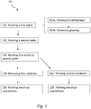
- Fig. 1 shows a general overview of the process steps of the method 100 of the present disclosure for providing a semiconductor device.
- the method 100 comprises a step 101 of forming (101) a first wafer (10) comprising a first substrate 11 of a group IV semiconductor, such as silicon, and a group III-V semiconductor device structure 12 formed by selective area epitaxial growth on a surface portion 13a of a front side 13 of the first substrate 11.
- Step 101 may for example comprise the steps of forming 101a an insulating layer 15 on the front side 13 of the first substrate 11.
- the surface portion 13a of the first substrate 11 may be exposed by a trench 16 in the insulating layer 15.
- Step 101 may also comprise epitaxially growing 101b the group III-V semiconductor device structure 12 on the surface portion 13a exposed by the trench 16.
- the method 100 also comprises a step 102 of forming a second wafer 20 comprising a second substrate 21 of a group IV semiconductor, such as silicon, and a group IV semiconductor device structure 22 formed on a front side 23 of the second substrate 21.
- the semiconductor structure may be configured such that the second wafer is an active wafer.
- the semiconductor structure may for example comprise CMOS based sensor and/or read-out circuit.
- the method 100 comprises bonding 103 the first wafer 10 to the second wafer 20 with the front side 13 of the first substrate 11 facing the front side 23 of the second wafer 21.
- the bonding 103 may comprise full wafer-to-wafer bonding.
- the method may comprise a step 104 of removing 104 the first substrate 11 to expose a base portion 17a of the group III-V semiconductor structure and a step of forming 105 electrical connections to said base portions 17a.
- Steps 104 and 105 may for example be relevant when the semiconductor device is a photo sensor and e.g. when the second wafer 20 comprises a CMOS sensor and/or read out circuitry.
- the method may after the step 103 of bonding the first wafer 10 to the second wafer 20 comprise a step of thinning 106 of the second substrate 21 and forming 107 electrical connections to said group IV semiconductor device structure 22.
- Steps 104 and 105 may for example be relevant when the second wafer 20 comprises a CMOS sensor and/or read out circuitry.
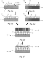
- Figs. 2a-f shows a schematic embodiment of a process architecture for preparing a semiconductor device in the form of a combined SWIR imager and imager for visible light (VIS).
- a first wafer 10 is formed by epitaxially growing at least one group III-V material on the front side 13a of a first silicon substrate 11 to form PIN diodes 12 on the silicon substrate ( Fig. 2a ).
- These diodes 12 may have a height of 0.5 - 4 ⁇ m and may be grown on a surface portions 13a that are in the form of trenches on the front side 13 of the silicon substrate 11.
- a second wafer 20 is of a silicon substrate 21 is formed having a group IV semiconductor device structure 22 in the form of VIS sensor/CMOS on a front side 23 of the substrate 21 ( Fig. 2b ).
- the visible sensor/CMOS may be for back illumination.
- Both the first substrate 11 and the second substrate 21 may then be planarized and prepared for hybrid bonding using Cu/Ox and Cu/SiC. Planarization may be performed using techniques known in the art, i.e. using a mechanical polishing to flatten the surface.
- the first wafer 10 and the second wafer 20 are bonded using hybrid bonding such that the front side 13 of the first substrate 11 faces the front side 23 of the second wafer 21. Then, the back side 24 of the second substrate 21 is thinned and electrical connections 33 are formed to the VIS sensor 22 of the second wafer 20 to prepare the back illuminated VIS sensor and SWIR imager ( Fig. 2f ).
- Figs. 3a-f shows a schematic embodiment of an alternative process architecture for preparing a semiconductor device in the form of a combined SWIR imager and imager for visible light (VIS).
- a first wafer 10 is formed by epitaxially growing at least one group III-V material on the front side 13a of a first silicon substrate 11 to form PIN diodes 12 on the silicon substrate ( Fig. 3a ).
- These diodes 12 may have a height of 0.5 - 4 ⁇ m and may be grown on a surface portions 13a that are in the form of trenches on the front side 13 of the silicon substrate 11.
- a second wafer 20 is of a silicon substrate 21 is formed having a group IV semiconductor device structure 22 in the form of VIS sensor/CMOS on a front side 23 of the substrate 21 ( Fig. 3b ).
- the visible sensor/CMOS may be for back illumination.
- Both the first substrate 11 and the second substrate 21 may be planarized and prepared for hybrid bonding using Cu/Ox and Cu/SiC. As illustrated in Fig. 3e , the first wafer 10 and the second wafer 20 are bonded using direct bonding such that the front side 13 of the first substrate 11 faces the front side 23 of the second wafer 21. Then, the back side 24 of the second substrate 21 is thinned and electrical connections 33 are formed to the VIS sensor 22 of the second wafer 20 to prepare the back illuminated VIS sensor and SWIR imager ( Fig. 3f ). As an alternative, the back side 24 of the second substrate 21 may thinned and cavity pads 34 may be formed ( Fig. 3g ).
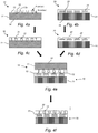
- Figs. 4a-f shows a schematic embodiment of a process architecture for preparing a semiconductor device in the form of a front illuminated sensor.
- a first wafer 10 is formed by epitaxially growing at least one group III-V material on the front side 13a of a first silicon substrate 11 to form PIN diodes 12 on the silicon substrate ( Fig. 4a ). These diodes 12 may have a height of 0.5 - 4 ⁇ m and may be grown on a surface portions 13a that are in the form of trenches on the front side 13 of the silicon substrate 11.
- a second wafer 20 is of a silicon substrate 21 is formed having a group IV semiconductor device structure 22 in the form of a visible sensor (FSI)/CMOS ROIC on a front side 23 of the substrate 21 ( Fig. 4b ).
- FSI visible sensor
- CMOS ROIC a visible sensor
- Both the first substrate 11 and the second substrate 21 may be planarized and prepared for hybrid bonding using Cu/Ox and Cu/SiC.
- the first wafer 10 and the second wafer 20 are bonded using hybrid bonding such that the front side 13 of the first substrate 11 faces the front side 23 of the second wafer 21.
- the back side 14 of the first substrate 11 is removed and electrical connections 33 are formed to the PIN diodes 12 and the second semiconductor structure 22 to prepare the CMOS/FSI imager made on silicon ( Fig. 4f ).
- Figs. 5a-f shows a schematic embodiment of an alternative process architecture for preparing semiconductor device in the form of a front illuminated sensor.
- a first wafer 10 is formed by epitaxially growing at least one group III-V material on the front side 13a of a first silicon substrate 11 to form PIN diodes 12 on the silicon substrate ( Fig. 5a ). These diodes 12 may have a height of 0.5 - 4 ⁇ m and may be grown on a surface portions 13a that are in the form of trenches on the front side 13 of the silicon substrate 11.
- a second wafer 20 is of a silicon substrate 21 is formed having a group IV semiconductor device structure 22 in the form of a visible sensor (FSI)/CMOS ROIC on a front side 23 of the substrate 21 ( Fig. 5b ).
- FSI visible sensor
- CMOS ROIC a visible sensor
- Contacts 31 to the PIN diodes 12 on the first wafer 10 may then be formed and the wafers 10 and 20 may then be prepared for wafer bonding ( Figs. 5c and 5d ).
- Both the first substrate 11 and the second substrate 21 may be planarized and prepared for hybrid bonding using Cu/Ox and Cu/SiC.
- the first wafer 10 and the second wafer 20 are bonded using direct bonding such that the front side 13 of the first substrate 11 faces the front side 23 of the second wafer 21.
- the back side 14 of the first substrate 11 is removed and electrical connections 33 are formed to the PIN diodes 12 and the second semiconductor structure 22 to form deep vias and N contacts ( Fig. 5f ).
- the back side 14 of the first substrate 11 is removed and cavity pads 34 and N contacts are formed, wherein the N contacts are interconnections vias ( Fig. 5g ).
- Figs. 6a-c is a schematic illustration of an embodiment of the selective area epitaxial growth of a group III-V semiconductor device structure 2 in trenches 16 of a front side 13 of a first substrate 11, such as silicon.
- trenches 16 may be formed in an insulating layer 15 so as to expose a surface portion 13a of the first substrate 11.
- the surface portion 13a at the bottom of the trench may have a cross-section perpendicular to the length of the trench in the form of an inverted pyramid.
- the trenches 16 may for example have a width that is between 60-100 nm, such as between 70-90 nm.
- the group III-V semiconductor device structure 12 such as a photodiode structure, may then be grown on the surface portion 13a exposed by the trench 16 using selective area epitaxial growth, such as aspect-ratio-tracking (ART), so as to form e.g. a diode structure 12, as illustrated in Fig. 6b .
- the method of forming the group III-V semiconductor device structure may comprise growing a lower narrow portion 17 in the trench 16 and an upper wider portion 18 protruding above the trench 16, as illustrated in the Fig. 6b .
- the photodiode structure 12 may further comprise an intrinsic portion 19 between the lower 17 and upper 18 diode portions.
- the lower diode portion 17 may be of a first conductive type extending from the surface portion 13a and protruding above the trench 16, whereas the upper diode portion 18 may be of a second conductivity type opposite to the first conductivity type.
- the distance between the trenches 16 and/or the epitaxial growth may be performed so that the semiconductor structures 12 merge above the trenches 16.
- the embodiment illustrated in Fig. 6c may be for forming a set of group III-V semiconductor photodiode structures 12 on a silicon wafer 11, wherein each photodiode structure 12 is formed by selective area growth on respective surface portions 13a of the front side 13 of the first substrate 11 exposed by a respective trench 16 in an insulating layer 15 formed on the front side 13 of the first substrate 11.
- each photodiode structure 12 may comprise a lower diode portion 17 of a first conductive type extending from the respective surface portion 13a and protruding above the trench 16, and an upper diode portion 18 of a second conductivity type opposite to the first conductivity type, and the photodiode structures 12 are formed to merge above the trenches 16.
- the epitaxial layers of the semiconductor structures grown on the first substrate 11 may for example be In x Ga 1-x As (0 ⁇ x ⁇ 100) and/or In x Ga 1-x Sb (0 ⁇ x ⁇ 100).
- the lower diode portion 17 could be a n+(p+)-Layer
- the intrinsic portion 19 could be a n - (p - )-Layer
- the upper diode portion 18 could be a p+(n+)-Layer.
- an insulating layer (not shown) could be deposited after growth of the diodes and contacts to the diodes 12 could be formed from Mo/AI, Ti/TiN, Ti/TiW, Ti/AI, Ti/TiN/Al, Ni/Ti or Pt/Ti/Au.
- the diodes could be embedded into a dielectric and planarized for further post processing and wafer bonding.
- the diodes 12 could also undego tapering (texturing) for increasing the absorbing volume of the semiconductor device 12. This may include enhancing the diode to increase absorption, since incident light may be bent more to a horizontal direction and thus remain in the material as compared to passing through more vertically.
- the device fabrication process started with the preparation of patterned Si substrates. First, rectangular trenches were realized in 300 nm thick SiO 2 layer on a 300mm Si (001) substrate using a standard shallow trench isolation (STI) process flow. Then the Si surface inside of the trenches were wet-etched with tetramethylammonium hydroxide (TMAH) to form V-shape ⁇ 111 ⁇ facets. These facets are suitable for the anti-phase domain free nucleation of III/V material directly on Si. After that the epitaxial growth of GaAs stack was performed by metal-organic chemical vapour phase deposition (MOCVD) method. The details of epitaxial growth and structural properties can be found in the publications Kunert et al, Appl. Phys. Let. 109, 091101 (2016 ) and Kunert et al, ECS Trans. (2016) 409-419 .
- MOCVD metal-organic chemical vapour phase deposition
- the epitaxy resulted in the growth of so-called nano ridge (NR) vertical diodes
- the epitaxial process started with the growth of ⁇ 200nm Si doped n-GaAs on phosphorus doped Si substrate. After that ⁇ 400nm of unintentionally doped GaAs with a p- background was grown, followed by ⁇ 100nm of the C-doped p-GaAs.
- the growth process was finalized by the growth of ⁇ 20nm GalnP, lattice matched unintentionally doped in-situ surface passivation layer all around device perimeter.
- the device fabrication comprised deposition of the Al 2 O 3 ex-situ passivation layer using atomic layer deposition (ALD) all around device perimeter. After that, a thick SiO 2 planarization layer was deposited using plasma enhanced atomic layer deposition (PEALD) and high-aspect-ratio process (HARP) atmospheric CVD, followed by the chemical mechanical polishing (CMP) step.
- PEALD plasma enhanced atomic layer deposition
- HTP high-aspect-ratio process
- CMP chemical mechanical polishing
- electrical contacts a combination of the wet etching and sputtering of Mo/Al or Ti/TiN/Al were used.
- the devices were biased using contacts to the top p-GaAs layer and n-Si substrate.
- the contact to the GaAs is 100 ⁇ m in diameter, thus contacting ⁇ 110 devices simultaneously on average.
- the leakage current measurements were performed on wafer level in the dark enclosure and controlled temperature.
- the dark current may be impacted by many physical parameters, e.g., temperature, bias, stress, defects, etc.
- Defects such as threading dislocations, are well known contributors to the leakage current of a diode.
- the threading dislocations density could be controlled by the proper choice of the epitaxial parameters, as well as, device geometry.
- the trench width was found to be an important geometrical parameter, as it allows control over defect density in the active region. With the purpose of TDD optimization, a set of diodes grown in the trenches of different width were fabricated. Fig. 7a and Fig. 7b show the leakage current measured on these pin-diodes.
- the dark current is strongly impacted by the choice of the trench width.
- the diodes grown in the wider trenches show higher dark current, while diodes grown in the narrower trenches show lower dark current.
- the reduction of dark current scales well with the reduction of the threading dislocations density as function of trench width.
Landscapes
- Solid State Image Pick-Up Elements (AREA)
Abstract
Description
- The present inventive concept relates to the field of forming semiconductor devices.
- More particularly it relates to a method of integrating semiconductor materials of group III-V into group III semiconductor manufacturing.
- Semiconductor materials of group III-V are alloys that contain elements from groups II and V of the periodic table, such as InP, InAs, GaAs, GaN, and InSb. They are for example widely used in optoelectronic devices due to their electronic properties, such as high electron mobility, direct band gap and low exciton binding energy. III-V materials may for example be used in PIN diodes that are implemented in Short-wavelength infrared (SWIR) imagers. However, SWIR imagers are usually made with wide band-gap materials that need to be bonded at die level with micro bumps and may further be associated with large costs.
- Unfortunately, direct growth of III-V materials, like e.g. GaAs, on standard Si (001) remains an integration process challenge and impacts significantly on device performance. This is due to the significant lattice mismatch and difference in the thermal expansion coefficients between e.g. GaAs and Si, of 4% and 60%, respectively. Moreover, direct nucleation of GaAs on Si poses the threat of undesirable antiphase domain formation.
- Consequently, semiconductor materials of group III-V may be difficult to grow on group III semiconductors, such as Si, and their processability and co-integration with e.g. Si Complementary metal-oxide-semiconductor (CMOS) technology is limited due to e.g. mismatch in thermal expansion (CTE) of die-bonded wafers.
- Thus, there is a need in the art for improved methods of integrating III-V materials, such as III-V PIN diodes, into a CMOS manufacturing line.
- It is an object of the invention to at least partly overcome one or more limitations of the prior art. In particular, it is an object to provide an improved method of bonding a wafer with a III-V material to a wafer with a group IV semiconductor.
- As a first aspect of the invention, there is provided a method comprising:
- forming a first wafer comprising a first substrate of a group IV semiconductor, and a group III-V semiconductor device structure formed by selective area epitaxial growth on a surface portion of a front side of the first substrate,
- forming a second wafer comprising a second substrate of a group IV semiconductor, and a group IV semiconductor device structure formed on a front side of the second substrate, and
- bonding the first wafer to the second wafer with the front side of the first substrate facing the front side of the second wafer.
- The first aspect provides an improved approach for integrating a group III-V semiconductor device structure into a group IV semiconductor manufacturing line. The inventors have found that the first wafer as formed according to the method may conveniently be bonded to the second wafer using conventional chip stacking techniques, such as wafer to wafer bonding. Using the method of the first aspect of the invention, the CTE mismatch between the substrates may be reduced. This allows for the production of e.g. SWIR imagers made with a wide band gap material in a CMOS production line.
- Thus, in embodiments of the first aspect, there is substantially no mismatch in thermal expansion coefficient (CTE) between the first and second substrates when bonding the first wafer to the second wafer.
- Forming of the first wafer may comprise forming the III-v semiconductor structure directly on silicon using heteroepitaxy.
- The group IV semiconductor device formed on the second substrate may comprise a CMOS based sensor and/or a readout circuit.
- The group III-V semiconductors referred to herein may be selected from InP, InGaAs, InAs, GaAs, AlAs, GaSb, AlSb, InSb, GaP, AIP, BAs, BP, BSb, GaN, AIN, InN, GaAsSb and ternary and quaternary combinations thereof.
- Further, the group IV semiconductor referred to herein may be chosen from Si, Ge, SiGe, SnGe or SnSi.
- In embodiments of the first aspect, the first substrate is a silicon substrate and/or the second substrate is a silicon substrate.
- Thus, only the first substrate may be a silicon substrate or only the second substrate may be a silicon substrate. As an alternative, both substrates may be silicon substrates.
- In embodiments of the first aspect, forming the first wafer comprises:
- forming an insulating layer on the front side of the first substrate, the surface portion of the first substrate being exposed by a trench in the insulating layer, and
- thereafter epitaxially growing the group III-V semiconductor device structure on the surface portion exposed by the trench.
- Thus, the formation of the first layer may comprise epitaxially growing the group III-V semiconductor device structure in trenches in the insulating layer on the first side of the first substrate. The growth may hence be formed by a dislocation trapping technique.
- As an example, forming the III-V semiconductor device structure formed by selective area epitaxial growth on a surface portion of a front side of the first substrate may be by Aspect Ratio Trapping (ART). This may reduce the terminating defects at the sidewalls of the patterned trenches that enclose the growth region.
- Thus, the ART technique allows trapping of dislocations originating from differences in lattice constant of the III-V semiconductor material and the group IV semiconductor. Accordingly, the trenches may be formed as a high aspect ratio aperture (i.e. having a vertical height greater than a width).
- As an example, forming the group III-V semiconductor device structure may comprise growing a lower narrow portion in the trench and an upper wider portion protruding above the trench.
- As an example, the group III-V semiconductor device structure forms a photodiode structure comprising a lower diode portion of a first conductive type extending from the surface portion and protruding above the trench, and an upper diode portion of a second conductivity type opposite to the first conductivity type.
- As an example, the photodiode structure may further comprise an intrinsic portion between the lower and upper diode portions.
- The method may thus be used for the formation of photodiode structures on the first wafer and integrating these structures with the second wafer, such as integrating the diode structures with a CMOS based second wafer. As an example, the method may be for formation of photodiodes having a sensitivity for wavelengths that are between 0.3 - 2.5 µm, such as between 0.4 to 2 µm, such as between 0.4 -1.6 µm.
- Consequently, the method of the first aspect is advantageous in that it may provide a sensor for detecting wavelengths between 0.3 - 2.5 µm, such as between 0.4 to 2 µm, such as between 0.4 -1.6 µm, using a single chip only, instead of using two different wafers manufactured using two different platforms.
- The shape of the protruding first portion may be selected so as to decrease leakage current.
- As an example, the width of at least one trench in the insulating layer is between 60-100 nm, such as between 70-90 nm.
- The inventors have found that by having the width of at least one trench, such as the width of all trenches, between 60-100 nm, such as between 70-90 nm, properties such as dark current and low defect density may be achieved.
- As a further example, the bottom of at least one trench may have the form of an inverted pyramid. This may be advantageous in that it may increase the amount of internal reflection and therefore also increase the quantum efficiency of the device.
- In embodiments of the first aspect, the first wafer comprises a set of group III-V semiconductor photodiode structures,
- each photodiode structure formed by selective area growth on respective surface portions of the front side of the first substrate exposed by a respective trench in an insulating layer formed on the front side of the first substrate, and
- each photodiode structure comprising a lower diode portion of a first conductive type extending from the respective surface portion and protruding above the trench, and an upper diode portion of a second conductivity type opposite to the first conductivity type, and
- wherein the photodiode structures are formed to merge above the trenches.
- In embodiments of the first aspect, bonding the first wafer to the second wafer with the front side of the first substrate facing the front side of the second wafer is performed without any additional patterning of the front side of the first substrate after selective area epitaxial growth on a surface portion of a front side of the first substrate
- Furthermore, in embodiments of the first aspect, the group IV semiconductor device structure formed on a front side of the second substrate is configured such that the second substrate is an active substrate.
- The group IV semiconductor device structure may be a CMOS structure and/or comprise read-out circuitry.
- In embodiments of the first aspect, the method is further comprising, subsequent to said bonding, removing the first substrate to expose a base portion of the group III-V semiconductor structure and forming electrical connections to said base portions. This step may for example be performed if a front illuminated sensor or a CMOS readout integrated circuit (ROIC) is produced by the method of the first aspect.
- In embodiments of the first aspect, the method is further comprising, subsequent to said bonding, thinning of said second substrate and forming electrical connections to said group IV semiconductor device structure. This step may for example be performed if a back illuminated module sensor for VIS and SWIR is produced by the method of the first aspect.
- According to some embodiments, the first and/or second handling wafer may have a wafer size of at least 300 mm.
- As a second aspect of the invention, there is provided a method for forming a diode structure on a wafer, said method comprising
- forming an insulating layer on the front side of the first substrate, the surface portion of the first substrate being exposed by a trench in the insulating layer, and
thereafter epitaxially growing a group III-V semiconductor diode structure on the surface portion exposed by the trench, - wherein the trench has a width that is between 60-100 nm, such as between 70-90 nm.
- The second aspect may be for formation of photodiodes having a sensitivity for wavelengths that are between 0.3 - 2.5 µm, such as between 0.4 to 2 µm, such as between 0.4 -1.6 µm.
- This aspect may generally present the same or corresponding advantages as the former aspect. Effects and features of this second aspect are largely analogous to those described above in connection with the first and second aspects. Embodiments mentioned in relation to the first aspects are largely compatible with the second aspect.
- In an embodiment of the second aspect, the group III-V semiconductor device structure forms a photodiode structure comprising a lower diode portion of a first conductive type extending from the surface portion and protruding above the trench, and an upper diode portion of a second conductivity type opposite to the first conductivity type.
- The above, as well as additional objects, features and advantages of the present inventive concept, will be better understood through the following illustrative and non-limiting detailed description, with reference to the appended drawings. In the drawings like reference numerals will be used for like elements unless stated otherwise.
-
Fig. 1 is an illustration of the process steps of a method of the present disclosure -
Figs. 2a-f is an illustration of an embodiment of the method of the present invention for forming an imaging device. -
Figs. 3a-g is an illustration of another embodiment of method of the present invention for forming an imaging device. -
Figs. 4a-f is an illustration of an embodiment of the method of the present invention for forming a front illuminated sensor. -
Figs. 5a-f is an illustration of another embodiment of the method of the present invention for forming a front illuminated sensor. -
Figs. 6a-e is an illustration of the formation of a diode. -
Figs. 7a and 7b show experimental results of the dark current measured of GaAs pin diodes as function of trench width at -1V (Fig. 6a ) and normal ambience (Fig. 6b ). -
Fig. 1 shows a general overview of the process steps of themethod 100 of the present disclosure for providing a semiconductor device. - The
method 100 comprises astep 101 of forming (101) a first wafer (10) comprising afirst substrate 11 of a group IV semiconductor, such as silicon, and a group III-Vsemiconductor device structure 12 formed by selective area epitaxial growth on asurface portion 13a of afront side 13 of thefirst substrate 11. Step 101 may for example comprise the steps of forming 101a an insulatinglayer 15 on thefront side 13 of thefirst substrate 11. Thesurface portion 13a of thefirst substrate 11 may be exposed by atrench 16 in the insulatinglayer 15. Step 101 may also comprise epitaxially growing 101b the group III-Vsemiconductor device structure 12 on thesurface portion 13a exposed by thetrench 16. - The
method 100 also comprises astep 102 of forming asecond wafer 20 comprising asecond substrate 21 of a group IV semiconductor, such as silicon, and a group IVsemiconductor device structure 22 formed on afront side 23 of thesecond substrate 21. The semiconductor structure may be configured such that the second wafer is an active wafer. The semiconductor structure may for example comprise CMOS based sensor and/or read-out circuit. - Moreover, the
method 100 comprises bonding 103 thefirst wafer 10 to thesecond wafer 20 with thefront side 13 of thefirst substrate 11 facing thefront side 23 of thesecond wafer 21. Thebonding 103 may comprise full wafer-to-wafer bonding. - Thereafter, the method may comprise a
step 104 of removing 104 thefirst substrate 11 to expose a base portion 17a of the group III-V semiconductor structure and a step of forming 105 electrical connections to said base portions 17a.Steps second wafer 20 comprises a CMOS sensor and/or read out circuitry. - Alternatively, or as a compliment, the method may after the
step 103 of bonding thefirst wafer 10 to thesecond wafer 20 comprise a step of thinning 106 of thesecond substrate 21 and forming 107 electrical connections to said group IVsemiconductor device structure 22.Steps second wafer 20 comprises a CMOS sensor and/or read out circuitry. -
Figs. 2a-f shows a schematic embodiment of a process architecture for preparing a semiconductor device in the form of a combined SWIR imager and imager for visible light (VIS). Afirst wafer 10 is formed by epitaxially growing at least one group III-V material on thefront side 13a of afirst silicon substrate 11 to formPIN diodes 12 on the silicon substrate (Fig. 2a ). Thesediodes 12 may have a height of 0.5 - 4 µm and may be grown on asurface portions 13a that are in the form of trenches on thefront side 13 of thesilicon substrate 11. Further, asecond wafer 20 is of asilicon substrate 21 is formed having a group IVsemiconductor device structure 22 in the form of VIS sensor/CMOS on afront side 23 of the substrate 21 (Fig. 2b ). The visible sensor/CMOS may be for back illumination. -
Contacts 31 to thePIN diodes 12 on the first wafer 10 (Fig. 2c ) andelectrical contacts 32 to theCMOS structure 22 on the second wafer 20 (Fig. 2d ) may then be formed. Both thefirst substrate 11 and thesecond substrate 21 may then be planarized and prepared for hybrid bonding using Cu/Ox and Cu/SiC. Planarization may be performed using techniques known in the art, i.e. using a mechanical polishing to flatten the surface. - As illustrated in
Fig. 2e , thefirst wafer 10 and thesecond wafer 20 are bonded using hybrid bonding such that thefront side 13 of thefirst substrate 11 faces thefront side 23 of thesecond wafer 21. Then, theback side 24 of thesecond substrate 21 is thinned andelectrical connections 33 are formed to the VISsensor 22 of thesecond wafer 20 to prepare the back illuminated VIS sensor and SWIR imager (Fig. 2f ). -
Figs. 3a-f shows a schematic embodiment of an alternative process architecture for preparing a semiconductor device in the form of a combined SWIR imager and imager for visible light (VIS). Afirst wafer 10 is formed by epitaxially growing at least one group III-V material on thefront side 13a of afirst silicon substrate 11 to formPIN diodes 12 on the silicon substrate (Fig. 3a ). Thesediodes 12 may have a height of 0.5 - 4 µm and may be grown on asurface portions 13a that are in the form of trenches on thefront side 13 of thesilicon substrate 11. Further, asecond wafer 20 is of asilicon substrate 21 is formed having a group IVsemiconductor device structure 22 in the form of VIS sensor/CMOS on afront side 23 of the substrate 21 (Fig. 3b ). The visible sensor/CMOS may be for back illumination. -
Contacts 31 to thePIN diodes 12 on thefirst wafer 10 may then be formed (Figs. 3c and 3d ), thereby forming a SWIR focal plane. Both thefirst substrate 11 and thesecond substrate 21 may be planarized and prepared for hybrid bonding using Cu/Ox and Cu/SiC. As illustrated inFig. 3e , thefirst wafer 10 and thesecond wafer 20 are bonded using direct bonding such that thefront side 13 of thefirst substrate 11 faces thefront side 23 of thesecond wafer 21. Then, theback side 24 of thesecond substrate 21 is thinned andelectrical connections 33 are formed to the VISsensor 22 of thesecond wafer 20 to prepare the back illuminated VIS sensor and SWIR imager (Fig. 3f ). As an alternative, theback side 24 of thesecond substrate 21 may thinned andcavity pads 34 may be formed (Fig. 3g ). -
Figs. 4a-f shows a schematic embodiment of a process architecture for preparing a semiconductor device in the form of a front illuminated sensor. Afirst wafer 10 is formed by epitaxially growing at least one group III-V material on thefront side 13a of afirst silicon substrate 11 to formPIN diodes 12 on the silicon substrate (Fig. 4a ). Thesediodes 12 may have a height of 0.5 - 4 µm and may be grown on asurface portions 13a that are in the form of trenches on thefront side 13 of thesilicon substrate 11. Further, asecond wafer 20 is of asilicon substrate 21 is formed having a group IVsemiconductor device structure 22 in the form of a visible sensor (FSI)/CMOS ROIC on afront side 23 of the substrate 21 (Fig. 4b ). -
Contacts 31 to thePIN diodes 12 on the first wafer 10 (Fig. 4c ) andelectrical contacts 32 to theCMOS structure 22 on the second wafer 20 (Fig. 4d ) may then be formed. Both thefirst substrate 11 and thesecond substrate 21 may be planarized and prepared for hybrid bonding using Cu/Ox and Cu/SiC. As illustrated inFig. 4e , thefirst wafer 10 and thesecond wafer 20 are bonded using hybrid bonding such that thefront side 13 of thefirst substrate 11 faces thefront side 23 of thesecond wafer 21. Then, theback side 14 of thefirst substrate 11 is removed andelectrical connections 33 are formed to thePIN diodes 12 and thesecond semiconductor structure 22 to prepare the CMOS/FSI imager made on silicon (Fig. 4f ). -
Figs. 5a-f shows a schematic embodiment of an alternative process architecture for preparing semiconductor device in the form of a front illuminated sensor. Afirst wafer 10 is formed by epitaxially growing at least one group III-V material on thefront side 13a of afirst silicon substrate 11 to formPIN diodes 12 on the silicon substrate (Fig. 5a ). Thesediodes 12 may have a height of 0.5 - 4 µm and may be grown on asurface portions 13a that are in the form of trenches on thefront side 13 of thesilicon substrate 11. Further, asecond wafer 20 is of asilicon substrate 21 is formed having a group IVsemiconductor device structure 22 in the form of a visible sensor (FSI)/CMOS ROIC on afront side 23 of the substrate 21 (Fig. 5b ). -
Contacts 31 to thePIN diodes 12 on thefirst wafer 10 may then be formed and thewafers Figs. 5c and 5d ). Both thefirst substrate 11 and thesecond substrate 21 may be planarized and prepared for hybrid bonding using Cu/Ox and Cu/SiC. As illustrated inFig. 5e , thefirst wafer 10 and thesecond wafer 20 are bonded using direct bonding such that thefront side 13 of thefirst substrate 11 faces thefront side 23 of thesecond wafer 21. Then, theback side 14 of thefirst substrate 11 is removed andelectrical connections 33 are formed to thePIN diodes 12 and thesecond semiconductor structure 22 to form deep vias and N contacts (Fig. 5f ). As an alternative, theback side 14 of thefirst substrate 11 is removed andcavity pads 34 and N contacts are formed, wherein the N contacts are interconnections vias (Fig. 5g ). -
Figs. 6a-c is a schematic illustration of an embodiment of the selective area epitaxial growth of a group III-V semiconductor device structure 2 intrenches 16 of afront side 13 of afirst substrate 11, such as silicon. As illustrated inFig. 6a ,trenches 16 may be formed in an insulatinglayer 15 so as to expose asurface portion 13a of thefirst substrate 11. Thesurface portion 13a at the bottom of the trench may have a cross-section perpendicular to the length of the trench in the form of an inverted pyramid. Thetrenches 16 may for example have a width that is between 60-100 nm, such as between 70-90 nm. - The group III-V
semiconductor device structure 12, such as a photodiode structure, may then be grown on thesurface portion 13a exposed by thetrench 16 using selective area epitaxial growth, such as aspect-ratio-tracking (ART), so as to form e.g. adiode structure 12, as illustrated inFig. 6b . The method of forming the group III-V semiconductor device structure may comprise growing a lowernarrow portion 17 in thetrench 16 and an upperwider portion 18 protruding above thetrench 16, as illustrated in theFig. 6b . Thephotodiode structure 12 may further comprise anintrinsic portion 19 between the lower 17 and upper 18 diode portions. Further, thelower diode portion 17 may be of a first conductive type extending from thesurface portion 13a and protruding above thetrench 16, whereas theupper diode portion 18 may be of a second conductivity type opposite to the first conductivity type. - As illustrated in
Fig. 6c , the distance between thetrenches 16 and/or the epitaxial growth may be performed so that thesemiconductor structures 12 merge above thetrenches 16. Thus, the embodiment illustrated inFig. 6c may be for forming a set of group III-Vsemiconductor photodiode structures 12 on asilicon wafer 11, wherein eachphotodiode structure 12 is formed by selective area growth onrespective surface portions 13a of thefront side 13 of thefirst substrate 11 exposed by arespective trench 16 in an insulatinglayer 15 formed on thefront side 13 of thefirst substrate 11. Further, eachphotodiode structure 12 may comprise alower diode portion 17 of a first conductive type extending from therespective surface portion 13a and protruding above thetrench 16, and anupper diode portion 18 of a second conductivity type opposite to the first conductivity type, and thephotodiode structures 12 are formed to merge above thetrenches 16. - The epitaxial layers of the semiconductor structures grown on the
first substrate 11 may for example be InxGa1-xAs (0≤x≤100) and/or InxGa1-xSb (0≤x≤100). - Further, the
lower diode portion 17 could be a n+(p+)-Layer, theintrinsic portion 19 could be a n-(p-)-Layer, and theupper diode portion 18 could be a p+(n+)-Layer. Also, an insulating layer (not shown) could be deposited after growth of the diodes and contacts to thediodes 12 could be formed from Mo/AI, Ti/TiN, Ti/TiW, Ti/AI, Ti/TiN/Al, Ni/Ti or Pt/Ti/Au. Thus, the diodes could be embedded into a dielectric and planarized for further post processing and wafer bonding. Thediodes 12 could also undego tapering (texturing) for increasing the absorbing volume of thesemiconductor device 12. This may include enhancing the diode to increase absorption, since incident light may be bent more to a horizontal direction and thus remain in the material as compared to passing through more vertically. - The device fabrication process started with the preparation of patterned Si substrates. First, rectangular trenches were realized in 300 nm thick SiO2 layer on a 300mm Si (001) substrate using a standard shallow trench isolation (STI) process flow. Then the Si surface inside of the trenches were wet-etched with tetramethylammonium hydroxide (TMAH) to form V-shape {111} facets. These facets are suitable for the anti-phase domain free nucleation of III/V material directly on Si. After that the epitaxial growth of GaAs stack was performed by metal-organic chemical vapour phase deposition (MOCVD) method. The details of epitaxial growth and structural properties can be found in the publications Kunert et al, Appl. Phys. Let. 109, 091101 (2016) and Kunert et al, ECS Trans. (2016) 409-419.
- The epitaxy resulted in the growth of so-called nano ridge (NR) vertical diodes The epitaxial process started with the growth of ∼200nm Si doped n-GaAs on phosphorus doped Si substrate. After that ∼400nm of unintentionally doped GaAs with a p- background was grown, followed by ∼100nm of the C-doped p-GaAs. The growth process was finalized by the growth of ∼20nm GalnP, lattice matched unintentionally doped in-situ surface passivation layer all around device perimeter.
- The device fabrication comprised deposition of the Al2O3 ex-situ passivation layer using atomic layer deposition (ALD) all around device perimeter. After that, a thick SiO2 planarization layer was deposited using plasma enhanced atomic layer deposition (PEALD) and high-aspect-ratio process (HARP) atmospheric CVD, followed by the chemical mechanical polishing (CMP) step. For the fabrication of electrical contacts, a combination of the wet etching and sputtering of Mo/Al or Ti/TiN/Al were used. The devices were biased using contacts to the top p-GaAs layer and n-Si substrate. The contact to the GaAs is 100 µm in diameter, thus contacting ∼ 110 devices simultaneously on average. The leakage current measurements were performed on wafer level in the dark enclosure and controlled temperature.
- The dark current may be impacted by many physical parameters, e.g., temperature, bias, stress, defects, etc. Defects, such as threading dislocations, are well known contributors to the leakage current of a diode. In the ART device growth method of the present disclosure, the threading dislocations density (TDD) could be controlled by the proper choice of the epitaxial parameters, as well as, device geometry. The trench width was found to be an important geometrical parameter, as it allows control over defect density in the active region. With the purpose of TDD optimization, a set of diodes grown in the trenches of different width were fabricated.
Fig. 7a and Fig. 7b show the leakage current measured on these pin-diodes. As one can see, the dark current is strongly impacted by the choice of the trench width. The diodes grown in the wider trenches show higher dark current, while diodes grown in the narrower trenches show lower dark current. The reduction of dark current scales well with the reduction of the threading dislocations density as function of trench width. - In the above the inventive concept has mainly been described with reference to a limited number of examples. However, as is readily appreciated by a person skilled in the art, other examples than the ones disclosed above are equally possible within the scope of the inventive concept, as defined by the appended claims.
Claims (12)
- A method (100) comprising:forming (101) a first wafer (10) comprising a first substrate (11) of a group IV semiconductor, and a group III-V semiconductor device structure (12) formed by selective area epitaxial growth on a surface portion (13a) of a front side (13) of the first substrate (11),forming (102) a second wafer (20) comprising a second substrate (21) of a group IV semiconductor, and a group IV semiconductor device structure (22) formed on a front side (23) of the second substrate (21), andbonding (103) the first wafer (10) to the second wafer (20) with the front side (13) of the first substrate (11) facing the front side (23) of the second wafer (21).
- A method (100) according to claim 1, wherein the first substrate (11) is a silicon substrate and/or the second substrate (21) is a silicon substrate.
- A method (100) according to any preceding claim, wherein forming (101) the first wafer (10) comprises:forming (101a) an insulating layer (15) on the front side (13) of the first substrate (11), the surface portion (13a) of the first substrate (11) being exposed by a trench (16) in the insulating layer (15), andthereafter epitaxially growing (101b) the group III-V semiconductor device structure (12) on the surface portion (13a) exposed by the trench (16).
- A method (100) according to claim 3, wherein forming (101b) the group III-V semiconductor device structure comprises growing a lower narrow portion (17) in the trench (16) and an upper wider portion (18) protruding above the trench (16).
- A method (100) according to claim 3 or 4, wherein the group III-V semiconductor device structure (12) forms a photodiode structure comprising a lower diode portion (17) of a first conductive type extending from the surface portion (13a) and protruding above the trench (16), and an upper diode portion (18) of a second conductivity type opposite to the first conductivity type.
- A method (100) according to claim 5, wherein the photodiode structure further comprises an intrinsic portion (19) between the lower (17) and upper (18) diode portions.
- A method (100) according to any one of claims 3-6, wherein the width of at least one trench (16) in the insulating layer (15) is between 60-100 nm, such as between 70-90 nm.
- A method (100) according to any preceding claim, wherein the first wafer (10) comprises a set of group III-V semiconductor photodiode structures,each photodiode structure (12) formed by selective area growth on respective surface portions (13a) of the front side (13) of the first substrate (11) exposed by a respective trench (16) in an insulating layer (15) formed on the front side (13) of the first substrate (11), andeach photodiode structure (12) comprising a lower diode portion (17) of a first conductive type extending from the respective surface portion (13a) and protruding above the trench (16), and an upper diode portion (18) of a second conductivity type opposite to the first conductivity type, andwherein the photodiode structures (12) are formed to merge above the trenches (16).
- A method (100) according to any previous claim, wherein the bonding (103) of the first wafer (10) to the second wafer (20) with the front side (13) of the first substrate (11) facing the front side (23) of the second wafer (20) is performed without any additional patterning of the front side (13) of the first substrate (11) after selective area epitaxial growth on a surface portion (13a) of a front side (13) of the first substrate (11).
- A method (100) according to any previous claim, wherein the group IV semiconductor device structure formed on a front side (23) of the second substrate (21) is configured such that the second substrate (21) is an active substrate (21).
- A method (100) according to any previous claim, further comprising, subsequent to said bonding (103), removing (104) the first substrate (11) to expose a base portion (17a) of the group III-V semiconductor structure and forming (105) electrical connections to said base portions (17a).
- A method (100) according to any one of claims 1-10, further comprising, subsequent to said bonding (103), thinning (106) of said second substrate (21) and forming (107) electrical connections to said group IV semiconductor device structure (22).
Priority Applications (2)
| Application Number | Priority Date | Filing Date | Title |
|---|---|---|---|
| EP19202647.4A EP3806152B1 (en) | 2019-10-11 | 2019-10-11 | A method of forming a semiconductor device structure |
| US17/068,785 US11282702B2 (en) | 2019-10-11 | 2020-10-12 | Method of forming a semiconductor device structure |
Applications Claiming Priority (1)
| Application Number | Priority Date | Filing Date | Title |
|---|---|---|---|
| EP19202647.4A EP3806152B1 (en) | 2019-10-11 | 2019-10-11 | A method of forming a semiconductor device structure |
Publications (2)
| Publication Number | Publication Date |
|---|---|
| EP3806152A1 true EP3806152A1 (en) | 2021-04-14 |
| EP3806152B1 EP3806152B1 (en) | 2022-08-24 |
Family
ID=68289807
Family Applications (1)
| Application Number | Title | Priority Date | Filing Date |
|---|---|---|---|
| EP19202647.4A Active EP3806152B1 (en) | 2019-10-11 | 2019-10-11 | A method of forming a semiconductor device structure |
Country Status (2)
| Country | Link |
|---|---|
| US (1) | US11282702B2 (en) |
| EP (1) | EP3806152B1 (en) |
Families Citing this family (2)
| Publication number | Priority date | Publication date | Assignee | Title |
|---|---|---|---|---|
| US12444672B2 (en) * | 2022-09-30 | 2025-10-14 | Intel Corporation | Hybrid bonding technologies with thermal expansion compensation structures |
| US20250231114A1 (en) * | 2024-01-17 | 2025-07-17 | Kla Corporation | Image sensor with oxide free wafer bonded structures and methods for fabricating image sensors |
Citations (1)
| Publication number | Priority date | Publication date | Assignee | Title |
|---|---|---|---|---|
| US20060006404A1 (en) * | 2004-06-30 | 2006-01-12 | James Ibbetson | Chip-scale methods for packaging light emitting devices and chip-scale packaged light emitting devices |
Family Cites Families (2)
| Publication number | Priority date | Publication date | Assignee | Title |
|---|---|---|---|---|
| US7977154B2 (en) * | 2006-04-14 | 2011-07-12 | Mississippi State University | Self-aligned methods based on low-temperature selective epitaxial growth for fabricating silicon carbide devices |
| US8304805B2 (en) | 2009-01-09 | 2012-11-06 | Taiwan Semiconductor Manufacturing Company, Ltd. | Semiconductor diodes fabricated by aspect ratio trapping with coalesced films |
-
2019
- 2019-10-11 EP EP19202647.4A patent/EP3806152B1/en active Active
-
2020
- 2020-10-12 US US17/068,785 patent/US11282702B2/en active Active
Patent Citations (1)
| Publication number | Priority date | Publication date | Assignee | Title |
|---|---|---|---|---|
| US20060006404A1 (en) * | 2004-06-30 | 2006-01-12 | James Ibbetson | Chip-scale methods for packaging light emitting devices and chip-scale packaged light emitting devices |
Non-Patent Citations (1)
| Title |
|---|
| KOEN DE MUNCK ET AL: "High performance Hybrid and Monolithic Backside Thinned CMOS Imagers realized using a new integration process", ELECTRON DEVICES MEETING, 2006. IEDM '06. INTERNATIONAL, IEEE, PI, 1 December 2006 (2006-12-01), pages 1 - 4, XP031078408, ISBN: 978-1-4244-0438-4 * |
Also Published As
| Publication number | Publication date |
|---|---|
| US11282702B2 (en) | 2022-03-22 |
| US20210111021A1 (en) | 2021-04-15 |
| EP3806152B1 (en) | 2022-08-24 |
Similar Documents
| Publication | Publication Date | Title |
|---|---|---|
| US20240355944A1 (en) | Photodetector | |
| KR101450956B1 (en) | Devices formed from a non-polar plane of a crystalline material and method of making the same | |
| TWI427830B (en) | Photoelectric device manufacturing method | |
| US20210119075A1 (en) | Process for manufacturing an optoelectronic device having a diode matrix | |
| US9105804B2 (en) | Method for manufacturing light-receiving device and light-receiving device | |
| US20160105247A1 (en) | Complementary metal oxide semiconductor device with iii-v optical interconnect having iii-v epitaxial semiconductor material formed using lateral overgrowth | |
| CN104576807A (en) | Semiconductor device | |
| CN115004372B (en) | Structural and materials engineering methods for enhancing the signal-to-noise ratio of optoelectronic devices | |
| US20250344525A1 (en) | Image sensor device and methods of forming the same | |
| JP2016092037A (en) | Semiconductor laminate, light receiving element and sensor | |
| KR102955624B1 (en) | A semiconductor device | |
| US11282702B2 (en) | Method of forming a semiconductor device structure | |
| JP6589662B2 (en) | Semiconductor laminate and light receiving element | |
| JP6613923B2 (en) | Semiconductor laminate, light receiving element, and method of manufacturing semiconductor laminate | |
| JP6477036B2 (en) | Semiconductor laminate and semiconductor device | |
| WO2025139385A1 (en) | Ingaas wafer and manufacturing method therefor, and radio frequency array chip and manufacturing method therefor | |
| CN115377135B (en) | Infrared detector, imaging chip and preparation method of imaging chip | |
| JP7147570B2 (en) | Semiconductor laminate and light receiving element | |
| US20260068337A1 (en) | Pixel structure | |
| US20230078458A1 (en) | Semiconductor device | |
| US20230395561A1 (en) | Method for Producing a Semiconductor Chip |
Legal Events
| Date | Code | Title | Description |
|---|---|---|---|
| PUAI | Public reference made under article 153(3) epc to a published international application that has entered the european phase |
Free format text: ORIGINAL CODE: 0009012 |
|
| STAA | Information on the status of an ep patent application or granted ep patent |
Free format text: STATUS: THE APPLICATION HAS BEEN PUBLISHED |
|
| AK | Designated contracting states |
Kind code of ref document: A1 Designated state(s): AL AT BE BG CH CY CZ DE DK EE ES FI FR GB GR HR HU IE IS IT LI LT LU LV MC MK MT NL NO PL PT RO RS SE SI SK SM TR |
|
| AX | Request for extension of the european patent |
Extension state: BA ME |
|
| STAA | Information on the status of an ep patent application or granted ep patent |
Free format text: STATUS: REQUEST FOR EXAMINATION WAS MADE |
|
| 17P | Request for examination filed |
Effective date: 20211011 |
|
| RBV | Designated contracting states (corrected) |
Designated state(s): AL AT BE BG CH CY CZ DE DK EE ES FI FR GB GR HR HU IE IS IT LI LT LU LV MC MK MT NL NO PL PT RO RS SE SI SK SM TR |
|
| GRAP | Despatch of communication of intention to grant a patent |
Free format text: ORIGINAL CODE: EPIDOSNIGR1 |
|
| STAA | Information on the status of an ep patent application or granted ep patent |
Free format text: STATUS: GRANT OF PATENT IS INTENDED |
|
| INTG | Intention to grant announced |
Effective date: 20220330 |
|
| GRAS | Grant fee paid |
Free format text: ORIGINAL CODE: EPIDOSNIGR3 |
|
| GRAA | (expected) grant |
Free format text: ORIGINAL CODE: 0009210 |
|
| STAA | Information on the status of an ep patent application or granted ep patent |
Free format text: STATUS: THE PATENT HAS BEEN GRANTED |
|
| AK | Designated contracting states |
Kind code of ref document: B1 Designated state(s): AL AT BE BG CH CY CZ DE DK EE ES FI FR GB GR HR HU IE IS IT LI LT LU LV MC MK MT NL NO PL PT RO RS SE SI SK SM TR |
|
| REG | Reference to a national code |
Ref country code: CH Ref legal event code: EP |
|
| REG | Reference to a national code |
Ref country code: DE Ref legal event code: R096 Ref document number: 602019018595 Country of ref document: DE |
|
| REG | Reference to a national code |
Ref country code: IE Ref legal event code: FG4D |
|
| REG | Reference to a national code |
Ref country code: AT Ref legal event code: REF Ref document number: 1514247 Country of ref document: AT Kind code of ref document: T Effective date: 20220915 |
|
| REG | Reference to a national code |
Ref country code: LT Ref legal event code: MG9D |
|
| REG | Reference to a national code |
Ref country code: NL Ref legal event code: MP Effective date: 20220824 |
|
| PG25 | Lapsed in a contracting state [announced via postgrant information from national office to epo] |
Ref country code: SE Free format text: LAPSE BECAUSE OF FAILURE TO SUBMIT A TRANSLATION OF THE DESCRIPTION OR TO PAY THE FEE WITHIN THE PRESCRIBED TIME-LIMIT Effective date: 20220824 Ref country code: RS Free format text: LAPSE BECAUSE OF FAILURE TO SUBMIT A TRANSLATION OF THE DESCRIPTION OR TO PAY THE FEE WITHIN THE PRESCRIBED TIME-LIMIT Effective date: 20220824 Ref country code: PT Free format text: LAPSE BECAUSE OF FAILURE TO SUBMIT A TRANSLATION OF THE DESCRIPTION OR TO PAY THE FEE WITHIN THE PRESCRIBED TIME-LIMIT Effective date: 20221226 Ref country code: NO Free format text: LAPSE BECAUSE OF FAILURE TO SUBMIT A TRANSLATION OF THE DESCRIPTION OR TO PAY THE FEE WITHIN THE PRESCRIBED TIME-LIMIT Effective date: 20221124 Ref country code: NL Free format text: LAPSE BECAUSE OF FAILURE TO SUBMIT A TRANSLATION OF THE DESCRIPTION OR TO PAY THE FEE WITHIN THE PRESCRIBED TIME-LIMIT Effective date: 20220824 Ref country code: LV Free format text: LAPSE BECAUSE OF FAILURE TO SUBMIT A TRANSLATION OF THE DESCRIPTION OR TO PAY THE FEE WITHIN THE PRESCRIBED TIME-LIMIT Effective date: 20220824 Ref country code: LT Free format text: LAPSE BECAUSE OF FAILURE TO SUBMIT A TRANSLATION OF THE DESCRIPTION OR TO PAY THE FEE WITHIN THE PRESCRIBED TIME-LIMIT Effective date: 20220824 Ref country code: FI Free format text: LAPSE BECAUSE OF FAILURE TO SUBMIT A TRANSLATION OF THE DESCRIPTION OR TO PAY THE FEE WITHIN THE PRESCRIBED TIME-LIMIT Effective date: 20220824 |
|
| REG | Reference to a national code |
Ref country code: AT Ref legal event code: MK05 Ref document number: 1514247 Country of ref document: AT Kind code of ref document: T Effective date: 20220824 |
|
| PG25 | Lapsed in a contracting state [announced via postgrant information from national office to epo] |
Ref country code: PL Free format text: LAPSE BECAUSE OF FAILURE TO SUBMIT A TRANSLATION OF THE DESCRIPTION OR TO PAY THE FEE WITHIN THE PRESCRIBED TIME-LIMIT Effective date: 20220824 Ref country code: IS Free format text: LAPSE BECAUSE OF FAILURE TO SUBMIT A TRANSLATION OF THE DESCRIPTION OR TO PAY THE FEE WITHIN THE PRESCRIBED TIME-LIMIT Effective date: 20221224 Ref country code: HR Free format text: LAPSE BECAUSE OF FAILURE TO SUBMIT A TRANSLATION OF THE DESCRIPTION OR TO PAY THE FEE WITHIN THE PRESCRIBED TIME-LIMIT Effective date: 20220824 Ref country code: GR Free format text: LAPSE BECAUSE OF FAILURE TO SUBMIT A TRANSLATION OF THE DESCRIPTION OR TO PAY THE FEE WITHIN THE PRESCRIBED TIME-LIMIT Effective date: 20221125 |
|
| PG25 | Lapsed in a contracting state [announced via postgrant information from national office to epo] |
Ref country code: SM Free format text: LAPSE BECAUSE OF FAILURE TO SUBMIT A TRANSLATION OF THE DESCRIPTION OR TO PAY THE FEE WITHIN THE PRESCRIBED TIME-LIMIT Effective date: 20220824 Ref country code: RO Free format text: LAPSE BECAUSE OF FAILURE TO SUBMIT A TRANSLATION OF THE DESCRIPTION OR TO PAY THE FEE WITHIN THE PRESCRIBED TIME-LIMIT Effective date: 20220824 Ref country code: ES Free format text: LAPSE BECAUSE OF FAILURE TO SUBMIT A TRANSLATION OF THE DESCRIPTION OR TO PAY THE FEE WITHIN THE PRESCRIBED TIME-LIMIT Effective date: 20220824 Ref country code: DK Free format text: LAPSE BECAUSE OF FAILURE TO SUBMIT A TRANSLATION OF THE DESCRIPTION OR TO PAY THE FEE WITHIN THE PRESCRIBED TIME-LIMIT Effective date: 20220824 Ref country code: CZ Free format text: LAPSE BECAUSE OF FAILURE TO SUBMIT A TRANSLATION OF THE DESCRIPTION OR TO PAY THE FEE WITHIN THE PRESCRIBED TIME-LIMIT Effective date: 20220824 Ref country code: AT Free format text: LAPSE BECAUSE OF FAILURE TO SUBMIT A TRANSLATION OF THE DESCRIPTION OR TO PAY THE FEE WITHIN THE PRESCRIBED TIME-LIMIT Effective date: 20220824 |
|
| REG | Reference to a national code |
Ref country code: DE Ref legal event code: R097 Ref document number: 602019018595 Country of ref document: DE |
|
| PG25 | Lapsed in a contracting state [announced via postgrant information from national office to epo] |
Ref country code: SK Free format text: LAPSE BECAUSE OF FAILURE TO SUBMIT A TRANSLATION OF THE DESCRIPTION OR TO PAY THE FEE WITHIN THE PRESCRIBED TIME-LIMIT Effective date: 20220824 Ref country code: MC Free format text: LAPSE BECAUSE OF FAILURE TO SUBMIT A TRANSLATION OF THE DESCRIPTION OR TO PAY THE FEE WITHIN THE PRESCRIBED TIME-LIMIT Effective date: 20220824 Ref country code: EE Free format text: LAPSE BECAUSE OF FAILURE TO SUBMIT A TRANSLATION OF THE DESCRIPTION OR TO PAY THE FEE WITHIN THE PRESCRIBED TIME-LIMIT Effective date: 20220824 |
|
| REG | Reference to a national code |
Ref country code: CH Ref legal event code: PL |
|
| P01 | Opt-out of the competence of the unified patent court (upc) registered |
Effective date: 20230513 |
|
| REG | Reference to a national code |
Ref country code: BE Ref legal event code: MM Effective date: 20221031 |
|
| PG25 | Lapsed in a contracting state [announced via postgrant information from national office to epo] |
Ref country code: LU Free format text: LAPSE BECAUSE OF NON-PAYMENT OF DUE FEES Effective date: 20221011 Ref country code: AL Free format text: LAPSE BECAUSE OF FAILURE TO SUBMIT A TRANSLATION OF THE DESCRIPTION OR TO PAY THE FEE WITHIN THE PRESCRIBED TIME-LIMIT Effective date: 20220824 |
|
| PLBE | No opposition filed within time limit |
Free format text: ORIGINAL CODE: 0009261 |
|
| STAA | Information on the status of an ep patent application or granted ep patent |
Free format text: STATUS: NO OPPOSITION FILED WITHIN TIME LIMIT |
|
| PG25 | Lapsed in a contracting state [announced via postgrant information from national office to epo] |
Ref country code: LI Free format text: LAPSE BECAUSE OF NON-PAYMENT OF DUE FEES Effective date: 20221031 Ref country code: FR Free format text: LAPSE BECAUSE OF NON-PAYMENT OF DUE FEES Effective date: 20221024 Ref country code: CH Free format text: LAPSE BECAUSE OF NON-PAYMENT OF DUE FEES Effective date: 20221031 |
|
| 26N | No opposition filed |
Effective date: 20230525 |
|
| PG25 | Lapsed in a contracting state [announced via postgrant information from national office to epo] |
Ref country code: SI Free format text: LAPSE BECAUSE OF FAILURE TO SUBMIT A TRANSLATION OF THE DESCRIPTION OR TO PAY THE FEE WITHIN THE PRESCRIBED TIME-LIMIT Effective date: 20220824 |
|
| PG25 | Lapsed in a contracting state [announced via postgrant information from national office to epo] |
Ref country code: BE Free format text: LAPSE BECAUSE OF NON-PAYMENT OF DUE FEES Effective date: 20221031 |
|
| PG25 | Lapsed in a contracting state [announced via postgrant information from national office to epo] |
Ref country code: IE Free format text: LAPSE BECAUSE OF NON-PAYMENT OF DUE FEES Effective date: 20221011 |
|
| PG25 | Lapsed in a contracting state [announced via postgrant information from national office to epo] |
Ref country code: CY Free format text: LAPSE BECAUSE OF FAILURE TO SUBMIT A TRANSLATION OF THE DESCRIPTION OR TO PAY THE FEE WITHIN THE PRESCRIBED TIME-LIMIT Effective date: 20220824 |
|
| PG25 | Lapsed in a contracting state [announced via postgrant information from national office to epo] |
Ref country code: MK Free format text: LAPSE BECAUSE OF FAILURE TO SUBMIT A TRANSLATION OF THE DESCRIPTION OR TO PAY THE FEE WITHIN THE PRESCRIBED TIME-LIMIT Effective date: 20220824 Ref country code: IT Free format text: LAPSE BECAUSE OF FAILURE TO SUBMIT A TRANSLATION OF THE DESCRIPTION OR TO PAY THE FEE WITHIN THE PRESCRIBED TIME-LIMIT Effective date: 20220824 Ref country code: HU Free format text: LAPSE BECAUSE OF FAILURE TO SUBMIT A TRANSLATION OF THE DESCRIPTION OR TO PAY THE FEE WITHIN THE PRESCRIBED TIME-LIMIT; INVALID AB INITIO Effective date: 20191011 |
|
| GBPC | Gb: european patent ceased through non-payment of renewal fee |
Effective date: 20231011 |
|
| PG25 | Lapsed in a contracting state [announced via postgrant information from national office to epo] |
Ref country code: TR Free format text: LAPSE BECAUSE OF FAILURE TO SUBMIT A TRANSLATION OF THE DESCRIPTION OR TO PAY THE FEE WITHIN THE PRESCRIBED TIME-LIMIT Effective date: 20220824 |
|
| PG25 | Lapsed in a contracting state [announced via postgrant information from national office to epo] |
Ref country code: GB Free format text: LAPSE BECAUSE OF NON-PAYMENT OF DUE FEES Effective date: 20231011 |
|
| PG25 | Lapsed in a contracting state [announced via postgrant information from national office to epo] |
Ref country code: GB Free format text: LAPSE BECAUSE OF NON-PAYMENT OF DUE FEES Effective date: 20231011 Ref country code: BG Free format text: LAPSE BECAUSE OF FAILURE TO SUBMIT A TRANSLATION OF THE DESCRIPTION OR TO PAY THE FEE WITHIN THE PRESCRIBED TIME-LIMIT Effective date: 20220824 |
|
| PG25 | Lapsed in a contracting state [announced via postgrant information from national office to epo] |
Ref country code: MT Free format text: LAPSE BECAUSE OF FAILURE TO SUBMIT A TRANSLATION OF THE DESCRIPTION OR TO PAY THE FEE WITHIN THE PRESCRIBED TIME-LIMIT Effective date: 20220824 |
|
| REG | Reference to a national code |
Ref country code: DE Ref legal event code: R079 Ref document number: 602019018595 Country of ref document: DE Free format text: PREVIOUS MAIN CLASS: H01L0027146000 Ipc: H10F0039180000 |
|
| PGFP | Annual fee paid to national office [announced via postgrant information from national office to epo] |
Ref country code: DE Payment date: 20250923 Year of fee payment: 7 |