EP3799328A1 - Procédé de conditionnement de signaux et dispositif associé - Google Patents
Procédé de conditionnement de signaux et dispositif associé Download PDFInfo
- Publication number
- EP3799328A1 EP3799328A1 EP20196624.9A EP20196624A EP3799328A1 EP 3799328 A1 EP3799328 A1 EP 3799328A1 EP 20196624 A EP20196624 A EP 20196624A EP 3799328 A1 EP3799328 A1 EP 3799328A1
- Authority
- EP
- European Patent Office
- Prior art keywords
- coupling
- coupling stage
- antennas
- power
- stage
- Prior art date
- Legal status (The legal status is an assumption and is not a legal conclusion. Google has not performed a legal analysis and makes no representation as to the accuracy of the status listed.)
- Granted
Links
Images

Classifications
-
- H—ELECTRICITY
- H04—ELECTRIC COMMUNICATION TECHNIQUE
- H04B—TRANSMISSION
- H04B7/00—Radio transmission systems, i.e. using radiation field
- H04B7/02—Diversity systems; Multi-antenna system, i.e. transmission or reception using multiple antennas
- H04B7/04—Diversity systems; Multi-antenna system, i.e. transmission or reception using multiple antennas using two or more spaced independent antennas
- H04B7/06—Diversity systems; Multi-antenna system, i.e. transmission or reception using multiple antennas using two or more spaced independent antennas at the transmitting station
- H04B7/0613—Diversity systems; Multi-antenna system, i.e. transmission or reception using multiple antennas using two or more spaced independent antennas at the transmitting station using simultaneous transmission
- H04B7/0615—Diversity systems; Multi-antenna system, i.e. transmission or reception using multiple antennas using two or more spaced independent antennas at the transmitting station using simultaneous transmission of weighted versions of same signal
- H04B7/0617—Diversity systems; Multi-antenna system, i.e. transmission or reception using multiple antennas using two or more spaced independent antennas at the transmitting station using simultaneous transmission of weighted versions of same signal for beam forming
-
- H—ELECTRICITY
- H03—ELECTRONIC CIRCUITRY
- H03G—CONTROL OF AMPLIFICATION
- H03G3/00—Gain control in amplifiers or frequency changers
- H03G3/20—Automatic control
- H03G3/30—Automatic control in amplifiers having semiconductor devices
- H03G3/3036—Automatic control in amplifiers having semiconductor devices in high-frequency amplifiers or in frequency-changers
- H03G3/3042—Automatic control in amplifiers having semiconductor devices in high-frequency amplifiers or in frequency-changers in modulators, frequency-changers, transmitters or power amplifiers
-
- H—ELECTRICITY
- H04—ELECTRIC COMMUNICATION TECHNIQUE
- H04B—TRANSMISSION
- H04B1/00—Details of transmission systems, not covered by a single one of groups H04B3/00 - H04B13/00; Details of transmission systems not characterised by the medium used for transmission
- H04B1/02—Transmitters
- H04B1/04—Circuits
-
- H—ELECTRICITY
- H01—ELECTRIC ELEMENTS
- H01Q—ANTENNAS, i.e. RADIO AERIALS
- H01Q3/00—Arrangements for changing or varying the orientation or the shape of the directional pattern of the waves radiated from an antenna or antenna system
- H01Q3/26—Arrangements for changing or varying the orientation or the shape of the directional pattern of the waves radiated from an antenna or antenna system varying the relative phase or relative amplitude of energisation between two or more active radiating elements; varying the distribution of energy across a radiating aperture
- H01Q3/28—Arrangements for changing or varying the orientation or the shape of the directional pattern of the waves radiated from an antenna or antenna system varying the relative phase or relative amplitude of energisation between two or more active radiating elements; varying the distribution of energy across a radiating aperture varying the amplitude
-
- H—ELECTRICITY
- H01—ELECTRIC ELEMENTS
- H01Q—ANTENNAS, i.e. RADIO AERIALS
- H01Q3/00—Arrangements for changing or varying the orientation or the shape of the directional pattern of the waves radiated from an antenna or antenna system
- H01Q3/26—Arrangements for changing or varying the orientation or the shape of the directional pattern of the waves radiated from an antenna or antenna system varying the relative phase or relative amplitude of energisation between two or more active radiating elements; varying the distribution of energy across a radiating aperture
- H01Q3/30—Arrangements for changing or varying the orientation or the shape of the directional pattern of the waves radiated from an antenna or antenna system varying the relative phase or relative amplitude of energisation between two or more active radiating elements; varying the distribution of energy across a radiating aperture varying the relative phase between the radiating elements of an array
- H01Q3/34—Arrangements for changing or varying the orientation or the shape of the directional pattern of the waves radiated from an antenna or antenna system varying the relative phase or relative amplitude of energisation between two or more active radiating elements; varying the distribution of energy across a radiating aperture varying the relative phase between the radiating elements of an array by electrical means
- H01Q3/36—Arrangements for changing or varying the orientation or the shape of the directional pattern of the waves radiated from an antenna or antenna system varying the relative phase or relative amplitude of energisation between two or more active radiating elements; varying the distribution of energy across a radiating aperture varying the relative phase between the radiating elements of an array by electrical means with variable phase-shifters
-
- H—ELECTRICITY
- H03—ELECTRONIC CIRCUITRY
- H03F—AMPLIFIERS
- H03F1/00—Details of amplifiers with only discharge tubes, only semiconductor devices or only unspecified devices as amplifying elements
- H03F1/02—Modifications of amplifiers to raise the efficiency, e.g. gliding Class A stages, use of an auxiliary oscillation
- H03F1/0205—Modifications of amplifiers to raise the efficiency, e.g. gliding Class A stages, use of an auxiliary oscillation in transistor amplifiers
- H03F1/0211—Modifications of amplifiers to raise the efficiency, e.g. gliding Class A stages, use of an auxiliary oscillation in transistor amplifiers with control of the supply voltage or current
-
- H—ELECTRICITY
- H03—ELECTRONIC CIRCUITRY
- H03F—AMPLIFIERS
- H03F1/00—Details of amplifiers with only discharge tubes, only semiconductor devices or only unspecified devices as amplifying elements
- H03F1/02—Modifications of amplifiers to raise the efficiency, e.g. gliding Class A stages, use of an auxiliary oscillation
- H03F1/0205—Modifications of amplifiers to raise the efficiency, e.g. gliding Class A stages, use of an auxiliary oscillation in transistor amplifiers
- H03F1/0294—Modifications of amplifiers to raise the efficiency, e.g. gliding Class A stages, use of an auxiliary oscillation in transistor amplifiers using vector summing of two or more constant amplitude phase-modulated signals
-
- H—ELECTRICITY
- H03—ELECTRONIC CIRCUITRY
- H03F—AMPLIFIERS
- H03F3/00—Amplifiers with only discharge tubes or only semiconductor devices as amplifying elements
- H03F3/20—Power amplifiers, e.g. Class B amplifiers, Class C amplifiers
- H03F3/21—Power amplifiers, e.g. Class B amplifiers, Class C amplifiers with semiconductor devices only
- H03F3/211—Power amplifiers, e.g. Class B amplifiers, Class C amplifiers with semiconductor devices only using a combination of several amplifiers
-
- H—ELECTRICITY
- H03—ELECTRONIC CIRCUITRY
- H03F—AMPLIFIERS
- H03F3/00—Amplifiers with only discharge tubes or only semiconductor devices as amplifying elements
- H03F3/20—Power amplifiers, e.g. Class B amplifiers, Class C amplifiers
- H03F3/24—Power amplifiers, e.g. Class B amplifiers, Class C amplifiers of transmitter output stages
- H03F3/245—Power amplifiers, e.g. Class B amplifiers, Class C amplifiers of transmitter output stages with semiconductor devices only
-
- H—ELECTRICITY
- H03—ELECTRONIC CIRCUITRY
- H03F—AMPLIFIERS
- H03F3/00—Amplifiers with only discharge tubes or only semiconductor devices as amplifying elements
- H03F3/60—Amplifiers in which coupling networks have distributed constants, e.g. with waveguide resonators
- H03F3/602—Combinations of several amplifiers
-
- H—ELECTRICITY
- H04—ELECTRIC COMMUNICATION TECHNIQUE
- H04B—TRANSMISSION
- H04B1/00—Details of transmission systems, not covered by a single one of groups H04B3/00 - H04B13/00; Details of transmission systems not characterised by the medium used for transmission
- H04B1/02—Transmitters
- H04B1/04—Circuits
- H04B1/0458—Arrangements for matching and coupling between power amplifier and antenna or between amplifying stages
-
- H—ELECTRICITY
- H04—ELECTRIC COMMUNICATION TECHNIQUE
- H04B—TRANSMISSION
- H04B1/00—Details of transmission systems, not covered by a single one of groups H04B3/00 - H04B13/00; Details of transmission systems not characterised by the medium used for transmission
- H04B1/02—Transmitters
- H04B1/04—Circuits
- H04B1/0483—Transmitters with multiple parallel paths
-
- H—ELECTRICITY
- H03—ELECTRONIC CIRCUITRY
- H03F—AMPLIFIERS
- H03F2200/00—Indexing scheme relating to amplifiers
- H03F2200/451—Indexing scheme relating to amplifiers the amplifier being a radio frequency amplifier
-
- H—ELECTRICITY
- H03—ELECTRONIC CIRCUITRY
- H03G—CONTROL OF AMPLIFICATION
- H03G2201/00—Indexing scheme relating to subclass H03G
- H03G2201/10—Gain control characterised by the type of controlled element
- H03G2201/103—Gain control characterised by the type of controlled element being an amplifying element
-
- H—ELECTRICITY
- H03—ELECTRONIC CIRCUITRY
- H03G—CONTROL OF AMPLIFICATION
- H03G2201/00—Indexing scheme relating to subclass H03G
- H03G2201/30—Gain control characterized by the type of controlled signal
- H03G2201/307—Gain control characterized by the type of controlled signal being radio frequency signal
-
- H—ELECTRICITY
- H04—ELECTRIC COMMUNICATION TECHNIQUE
- H04B—TRANSMISSION
- H04B1/00—Details of transmission systems, not covered by a single one of groups H04B3/00 - H04B13/00; Details of transmission systems not characterised by the medium used for transmission
- H04B1/02—Transmitters
- H04B1/04—Circuits
- H04B2001/0408—Circuits with power amplifiers
- H04B2001/0416—Circuits with power amplifiers having gain or transmission power control
Definitions
- Embodiments and embodiments of the invention relate to electronic devices dedicated to information transmissions, in particular for radiofrequency applications (“radio frequency”: RF in English) and more particularly to electronic devices comprising hybrid couplers. (“Hybrid couplers" in English).
- an electronic device dedicated to the radio transmission of information comprises a transmission chain comprising several transmission lines each connected to an antenna.
- Each transmission line performs in particular spatial filtering operations (“beamforming” in English) making it possible to control the phase and amplitude of the signals emitted by each antenna of the electronic device in order to create constructive or destructive interference between the emitted electromagnetic waves.
- a signal intended to be transmitted by an antenna passes through the transmission line comprising a first variable gain amplifier connected to a phase shifter, a first and a second hybrid coupling stages operating respectively as a power divider and as a power combiner, the two stages each comprising two inputs and two outputs, each output of the first coupling stage being connected to an input of the second coupling stage by a second variable gain power amplifier.
- the phase shifter is connected to a first input of the first coupling stage, the second input being connected to a first ballast resistor.
- a first output of the second stage is connected to the antenna, the second output being connected to a second ballast resistor.
- each transmission line consumes electrical power to ensure spatial filtering, in particular the first power amplifier and phase shifter, the electric power consumption is proportional to the number of antennas of the device (array of antennas).
- each transmission line occupies space on the silicon.
- a method of conditioning signals transmitted by at least two antennas from a power input signal comprising a first coupling stage comprising a divider. 90 ° power and a second coupling stage comprising a 90 ° power combiner, and variable gain power amplification means, each coupling stage comprising two inputs and two outputs, the two inputs of the first coupling stage receiving said power input signal, each output of the first coupling stage being connected to a different input of the second coupling stage by means of variable gain power amplification means, each output of the second coupling stage being connected to a different antenna, the method comprising determining the gains of the amplifying means as a function of the characteristics of the power input signal, the chars characteristics of the signals emitted by the antennas, and characteristics of the coupling stages.
- Signal conditioning is therefore understood here as being the steps contributing to the development of the signals emitted by the antennas from a power input signal.
- the coupling of the two inputs and outputs of the first and second coupling stages of the transmission paths make it possible to phase-shift and amplify the signals transmitted by the antennas without the implementation of a phase shifter, thus reducing consumption and bulk on the silicon of the paths transmission, the couplers operating as a phase shifter, the phase shift being controlled by adjusting the gains of the amplification means.
- the characteristics of the power input signal include the amplitude and the phase shift of said signal
- the characteristics of the signals transmitted by the antennas include the amplitude and the phase shift of the signals transmitted with respect to a reference signal
- the phase shift varies within an interval of -35 ° to + 35 ° with respect to the reference signal.
- the characteristics of the coupling stages include a loss coefficient of each coupling stage.
- the method comprises determining the gain of phase-shifting means connected to at least one input of the first coupling stage as a function of the characteristics of the power input signal, of the characteristics of the signals emitted by the antennas, and characteristics of the coupling stages.
- phase shift means makes it possible to extend the phase shift over a wider interval than that defined between -35 ° to + 35 °.
- the method comprises a first adjustment of the identical gains of the first transmission path connected to the two antennas emitting identical signals forming a reference signal and at least one second adjustment of the gains of at least one.
- second transmission path connected to two antennas each emitting a phase-shifted signal with respect to the reference signal.
- an electronic device comprising at least two antennas intended to transmit signals, and at least one transmission path, the transmission path comprising a first coupling stage comprising a 90 ° power divider and a second coupling stage comprising a 90 ° power combiner, and variable gain power amplification means, each coupling stage comprising two inputs and two outputs, the two inputs of the first coupling stage being intended to receive a power input signal, each output of the first coupling stage being connected to a different input of the second coupling stage via the amplification means variable gain power, each output of the second coupling stage being connected to a different antenna, the electronic device comprising control means configured to control the gains of the variable gain power amplification means as a function of the characteristics of the signal d power input, characteristics of the signals emitted by the antennas and characteristics of the coupling stages.
- the characteristics of the power input signal include the amplitude and the phase shift of said signal
- the characteristics of the signals emitted by the antennas include the amplitude and the phase shift of the signals emitted with respect to a signal of reference.
- the characteristics of the coupling stages include a loss coefficient of each coupling stage.
- At least one input of the first coupling stage comprises phase shift means controlled by the control means.
- variable gain power amplification means comprise two passive or active amplification means connecting, each means connecting an output of the first coupling stage to a different input of the second coupling stage.
- the passive variable gain power amplification means comprise at least one network of transistors.
- the active variable gain power amplification means comprise at least one variable gain power amplifier.
- a wireless communication device incorporating at least one device as defined above.
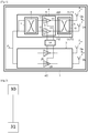
- the AC reference shown on the figure 1 represents a wireless communication device, here for example a cellular mobile telephone comprising at least one electronic device 1, here for example a millimeter radiofrequency device 1 produced in an integrated manner.
- Device 1 comprises two transmission paths 2 and 3 of identical architecture.
- a first transmission path 2 is coupled to two antennas 2a and 2b, and the second transmission path 3 is coupled to two antennas 3a and 3b.
- Device 1 comprises a matrix of two times two antennas.
- the device 1 can include one or more than two transmission paths each coupled to two antennas.
- Transmission paths 2 and 3 can be configured to emit an RF signal or receive an RF signal through the antennas 2a, 2b, 3a, 3b.
- the first transmission path 2 comprises variable gain power amplification means comprising an amplifier stage 4 comprising active elements, for example a first variable gain power amplifier 5 G5 and a second variable gain power amplifier 6 G6 coupled in parallel between a first coupling stage 7 and a second coupling stage 8.
- variable gain power amplification means comprising an amplifier stage 4 comprising active elements, for example a first variable gain power amplifier 5 G5 and a second variable gain power amplifier 6 G6 coupled in parallel between a first coupling stage 7 and a second coupling stage 8.
- the first coupling stage 7 comprises a first hybrid quadrature coupler, here for example a 90 ° power divider referenced 9 of which a first input and a second input are intended to receive a power input signal Pin, including a first output is coupled to the input 11 of the first amplifier 5, and a second output of which is coupled to the input 12 of the second amplifier 6.
- a first hybrid quadrature coupler here for example a 90 ° power divider referenced 9 of which a first input and a second input are intended to receive a power input signal Pin, including a first output is coupled to the input 11 of the first amplifier 5, and a second output of which is coupled to the input 12 of the second amplifier 6.
- the power of the input signal Pin is distributed equally, via the power divider 9, between the first and second outputs of the power divider 9, with a zero phase shift between these first and second outputs.
- the first coupling stage 7 has a first loss coefficient ⁇ 1 equal for example to 1dB.
- the second coupling stage 8 comprises a second hybrid quadrature coupler, here for example a 90 ° power combiner referenced 13 of which a first input terminal IN1 is coupled to the output 14 of the first amplifier 5, of which a second terminal of input IN2 is coupled to the output 15 of the second amplifier 6, of which a first output terminal OUT1 is coupled to the antenna 2a and of which a second output terminal OUT2 is coupled to the antenna 2b.
- a second hybrid quadrature coupler here for example a 90 ° power combiner referenced 13 of which a first input terminal IN1 is coupled to the output 14 of the first amplifier 5, of which a second terminal of input IN2 is coupled to the output 15 of the second amplifier 6, of which a first output terminal OUT1 is coupled to the antenna 2a and of which a second output terminal OUT2 is coupled to the antenna 2b.
- the device 1 further comprises control means 14 configured to control the gain of each power amplifier 5, 6 as a function of the characteristics of the power input signal Pin, characteristics of signals S2a, S2b emitted by antennas 2a and 2b, and characteristics of coupling stages 7 and 8.
- the control means 14 comprise for example a processing unit configured to control the gain of each power amplifier 5, 6 as a function of the characteristics of the power input signal Pin, of the characteristics of the signals S2a, S2b emitted by the antennas 2a and 2b, and characteristics of the coupling stages 7 and 8, and produced for example from a microcontroller.
- the power transmitted to each antenna 2a and 2b is equal to the combination of the powers of the output signals of amplifiers 5 and 6, phase-shifted or not phase-shifted with respect to the input signal Pin depending on whether the gains of amplifiers 5 and 6 are equal or not as illustrated in the following.
- the second coupling stage 8 has a second loss coefficient ⁇ 2 equal for example to the first loss coefficient ⁇ 1.
- the power amplifying means of the second transmission path 3 comprise a first power amplifier 25 of variable gain G25 and a second power amplifier 26 of gain G26.
- control means 14 are further configured to drive the first power amplifier 25 of variable gain G25 and the second power amplifier 26 of gain G26 of the second transmission path 3, as a function of the characteristics of the input signal. power Pin, the characteristics of the signals S3a, S3b emitted by the antennas 3a and 3b, and the characteristics of the coupling stages 7 and 8 of the second transmission path 3.
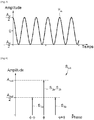
- the power input signal Pin is for example a sinusoidal signal of amplitude Ain centered on zero of frequency Fc as shown in figure 3 .
- the device 1 transmits for example an output signal S out of frequency Fc from the power input signal Pin, the figure 4 representing the line spectrum of the output signal S out as a function of the phase.
- the signal S out comprises a fundamental of amplitude A out with a phase ⁇ and two lines of amplitude A out / 2 with respectively a phase ⁇ - ⁇ and ⁇ + ⁇ , ⁇ being a predetermined phase shift with respect to the frequency of the signal Pine. It is assumed that the antennas 2a and 2b emit the fundamental and the antennas 3a and 3b emit the two amplitude lines A out / 2 out of phase with respect to the amplitude line A out .
- control means 14 determine the value of the gains G5 and G6 of the first transmission path 2 so that the antennas 2a and 2b together transmit a reference signal of amplitude A out corresponding to the fundamental of the signal S out .
- control means 14 determine the value of the gains G25 and G26 so that the antennas 3a and 3b emit the two amplitude lines A out / 2 respectively phase-shifted by + ⁇ and - ⁇ with respect to the signal reference.
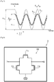
- the figure 5 illustrates a representation of the signals S2a and S2b forming the reference signal transmitted by the antennas 2a and 2b, and of the signals S3a and S3b transmitted by the antennas 3a and 3b.
- the coupling of the two inputs and outputs of the first and second coupling stages of the transmission paths 2, 3 make it possible to phase shift and amplify the signals emitted by the antennas without the implementation of a phase shifter, thus reducing consumption and bulk on the silicon of the transmission paths, the couplers functioning as a phase shifter, the phase shift being controlled by adjusting the gains of the amplification stages 4.
- variable gain power amplification means can comprise passive elements, for example networks of switchable transistors driven by the control means 14, configured to obtain the desired phase shift ⁇ by replacing power amplifiers with variable gain, a network of transistors replacing a power amplifier with variable gain.
- the signals emitted by the antennas are not amplified.
- the figure 6 illustrates a network of transistors 32 comprising three transistors T1, T2 and T3 whose gates are connected to the control means, the drains of transistors T1 and T2 are connected to each other and to an output of the first coupling stage 7, the source of the transistor T1 and the drain of transistor T3 are connected to an input of the second coupling stage 8, and the sources of transistors T2 and T3 are connected to a reference potential Vref chosen according to the value of the gain of network 32.
- phase shift ⁇ varies within an interval of -35 ° to + 35 ° with respect to the signal Pin.
- the figure 7 illustrates another embodiment of the device 1 making it possible to obtain a phase shift ⁇ outside the range of -35 ° to + 35 °.
- phase shifting means 33 controlled by control means 14 are inserted at the input of transmission paths 2 and 3.
- the phase shift means 33 make it possible to pre-phase the signal Pin.
Landscapes
- Engineering & Computer Science (AREA)
- Power Engineering (AREA)
- Computer Networks & Wireless Communication (AREA)
- Signal Processing (AREA)
- Amplifiers (AREA)
- Transmitters (AREA)
- Variable-Direction Aerials And Aerial Arrays (AREA)
Abstract
Description
- Des modes de mise en œuvre et de réalisation de l'invention concernent les dispositifs électroniques dédiés aux transmissions d'information, en particulier pour les applications radiofréquences (« radio frequency » : RF en anglais) et plus particulièrement des dispositifs électroniques comprenant des coupleurs hybrides (« hybrid couplers » en anglais).
- Généralement un dispositif électronique dédié à la transmission radio d'informations comprend une chaîne de transmission comportant plusieurs lignes de transmission reliées chacune à une antenne.
- Chaque ligne de transmission effectue notamment des opérations de filtrage spatial (« beamforming » en anglais) permettant de contrôler la phase et l'amplitude des signaux émis par chaque antenne du dispositif électronique pour créer des interférences constructives ou destructives entre les ondes électromagnétiques émises.
- Généralement un signal destiné à être émis par une antenne transite à travers la ligne de transmission comprenant un premier amplificateur à gain variable relié à un déphaseur, un premier et un deuxième étages de couplage hybride fonctionnant respectivement en diviseur de puissance et en combineur de puissance, les deux étages comportant chacun deux entrées et deux sorties, chaque sortie du premier étage de couplage étant reliée à une entrée du deuxième étage de couplage par un deuxième amplificateur de puissance à gain variable.
- Le déphaseur est relié à une première entrée du premier étage de couplage, la deuxième entrée étant reliée à une première résistance de ballast.
- Une première sortie du deuxième étage est reliée à l'antenne, la deuxième sortie étant reliée à une deuxième résistance de ballast.
- Cependant, chaque ligne de transmission consomme de la puissance électrique pour assurer le filtrage spatial, notamment le premier amplificateur de puissance et le déphaseur, la consommation de puissance électrique est proportionnelle au nombre d'antennes du dispositif (matrice d'antennes).
- En outre, l'implantation de chaque ligne de transmission occupe de la place sur le silicium.
- Il existe ainsi un besoin de proposer une solution technique permettant de diminuer la consommation des opérations de filtrage spatial réalisées par la chaîne de transmission tout en réduisant la place occupée par ladite chaîne sur le silicium.
- Selon un aspect, il est proposé un procédé de conditionnement de signaux émis par au moins deux antennes à partir d'un signal d'entrée de puissance, les deux antennes étant reliées à un chemin de transmission comprenant un premier étage de couplage comportant un diviseur de puissance 90° et un deuxième étage de couplage comportant un combineur de puissance 90°, et des moyens d'amplification de puissance à gain variable, chaque étage de couplage comportant deux entrées et deux sorties, les deux entrées du premier étage de couplage recevant ledit signal d'entrée de puissance, chaque sortie du premier étage de couplage étant reliée à une entrée différente du deuxième étage de couplage par l'intermédiaire des moyens d'amplification de puissance à gain variable, chaque sortie du deuxième étage de couplage étant reliée à une antenne différente, le procédé comprenant la détermination des gains des moyens d'amplification en fonction des caractéristiques du signal d'entrée de puissance, des caractéristiques des signaux émis par les antennes, et des caractéristiques des étages de couplage.
- Le conditionnement des signaux s'entend donc ici comme étant les étapes contribuant à l'élaboration des signaux émis par les antennes à partir d'un signal d'entrée de puissance.
- Le couplage des deux entrées et sorties des premier et deuxième étages de couplage des chemins de transmission permettent de déphaser et amplifier les signaux émis par les antennes sans l'implémentation d'un déphaseur réduisant ainsi la consommation et l'encombrement sur le silicium des chemins de transmission, les coupleurs fonctionnant comme déphaseur, le déphasage étant piloté en ajustant les gains des moyens d'amplification.
- Selon un mode de mise en œuvre, les caractéristiques du signal d'entrée de puissance comprennent l'amplitude et le déphasage dudit signal, et les caractéristiques des signaux émis par les antennes comprennent l'amplitude et le déphasage des signaux émis par rapport à un signal de référence.
- Le déphasage varie dans un intervalle de -35° à +35° par rapport au signal de référence.
- Selon autre un mode de mise en œuvre, les caractéristiques des étages de couplage comprennent un coefficient de perte de chaque étage de couplage.
- Selon encore autre un mode de mise en œuvre, le procédé comprend la détermination du gain de moyens de déphasage reliés à au moins une entrée du premier étage de couplage en fonction des caractéristiques du signal d'entrée de puissance, des caractéristiques des signaux émis par les antennes, et des caractéristiques des étages de couplage.
- L'ajout des moyens de déphasage permet d'étendre le déphasage su un intervalle plus large que celui défini entre -35° à +35°.
- Selon encore autre un mode de mise en œuvre, le procédé comprend un premier réglage des gains identiques du premier chemin de transmission relié aux deux antennes émettant des signaux identiques formant un signal de référence et au moins un deuxième réglage des gains d'au moins un deuxième chemin de transmission relié à deux antennes émettant chacun un signal déphasé par rapport au signal de référence.
- Selon un autre aspect, il est proposé un dispositif électronique, comprenant au moins deux antennes destinées à émettre des signaux, et au moins un chemin de transmission, le chemin de transmission comportant un premier étage de couplage comportant un diviseur de puissance 90° et un deuxième étage de couplage comportant un combineur de puissance 90°, et des moyens d'amplification de puissance à gain variable, chaque étage de couplage comportant deux entrées et deux sorties, les deux entrées du premier étage de couplage étant destinées à recevoir un signal d'entrée de puissance, chaque sortie du premier étage de couplage étant reliée à une entrée différente du deuxième étage de couplage par l'intermédiaire des moyens d'amplification de puissance à gain variable, chaque sortie du deuxième étage de couplage étant reliée à une antenne différente, le dispositif électronique comportant des moyens de commande configurés pour piloter les gains des moyens d'amplification de puissance à gain variable en fonction des caractéristiques du signal d'entrée de puissance, des caractéristiques des signaux émis par les antennes et des caractéristiques des étages de couplage.
- Selon un mode de réalisation, les caractéristiques du signal d'entrée de puissance comprennent l'amplitude et le déphasage dudit signal, et les caractéristiques des signaux émis par les antennes comprennent l'amplitude et le déphasage des signaux émis par rapport à un signal de référence.
- Selon un autre mode de réalisation, les caractéristiques des étages de couplage comprennent un coefficient de perte de chaque étage de couplage.
- Selon encore un autre mode de réalisation, au moins une entrée du premier étage de couplage comprend des moyens de déphasage pilotés par les moyens de commande.
- Selon encore un autre mode de réalisation, les moyens d'amplification de puissance à gain variable comprennent deux moyens d'amplification passifs ou actifs reliant, chaque moyen reliant une sortie du premier étage de couplage à une entrée différente du deuxième étage de couplage.
- Selon encore un autre mode de réalisation, les moyens d'amplification de puissance à gain variable passifs comprennent au moins un réseau de transistors.
- Selon encore un autre mode de réalisation, les moyens d'amplification de puissance à gain variable actifs comprennent au moins un amplificateur de puissance à gain variable.
- Selon encore un autre aspect, il est proposé un appareil de communication sans fil incorporant au moins un dispositif tel que défini ci-avant.
- D'autres avantages et caractéristiques de l'invention apparaîtront à l'examen de la description détaillée de modes de mise en œuvre et de réalisation, nullement limitatifs, et des dessins annexés sur lesquels :
- [
Fig 1 ] - [
Fig 2 ] - [
Fig 3 ] - [
Fig 4 ] - [
Fig 5 ] - [
Fig 6 ], et - [
Fig 7 ] - La référence AC illustrée sur la
figure 1 représente un appareil de communication sans fil, ici par exemple un téléphone portable cellulaire comportant au moins un dispositif électronique 1, ici par exemple un dispositif 1 radiofréquence millimétrique réalisé de façon intégré. - Le dispositif 1 comporte deux chemins de transmission 2 et 3 d'architecture identique.
- Un premier chemin de transmission 2 est couplé à deux antennes 2a et 2b, et le deuxième chemin de transmission 3 est couplé à deux antennes 3a et 3b.
- Le dispositif 1 comporte une matrice de deux fois deux antennes.
- Bien entendu, le dispositif 1 peut comporter un ou plus de deux chemins de transmission couplés chacun à deux antennes.
- Les chemins de transmission 2 et 3 peuvent être configurés pour émettre un signal RF ou recevoir un signal RF via les antennes 2a, 2b, 3a, 3b.
- A des fins de simplification et de clarté, comme les chemins de transmission 2 et 3 sont identiques, seul le premier chemin de transmission 2 est détaillé dans ce qui suit.
- Le premier chemin de transmission 2 comprend des moyens d'amplification de puissance à gain variable comprenant un étage amplificateur 4 comportant des éléments actifs par exemple un premier amplificateur de puissance 5 à gain variable G5 et un deuxième amplificateur de puissance 6 à gain variable G6 couplés en parallèle entre un premier étage de couplage 7 et un deuxième étage de couplage 8.
- Le premier étage de couplage 7 comprend un premier coupleur en quadrature hybride, ici par exemple un diviseur de puissance 90° référencé 9 dont une première entrée et une deuxième entrée sont destinées à recevoir un signal d'entrée de puissance Pin, dont une première sortie est couplée à l'entrée 11 du premier amplificateur 5, et dont une deuxième sortie est couplée à l'entrée 12 du deuxième amplificateur 6.
- Dans un cas idéal, la puissance du signal d'entrée Pin est distribuée également, via le diviseur de puissance 9, entre les première et deuxième sorties du diviseur de puissance 9, avec un déphasage nul entre ces première et deuxième sorties.
- Généralement le premier étage de couplage 7 présente un premier coefficient de perte η1 égal par exemple à 1dB.
- Le deuxième étage de couplage 8 comprend un deuxième coupleur en quadrature hybride, ici par exemple un combineur de puissance 90° référencé 13 dont une première borne d'entrée IN1 est couplée à la sortie 14 du premier amplificateur 5, dont une deuxième borne d'entrée IN2 est couplée à la sortie 15 du deuxième amplificateur 6, dont une première borne de sortie OUT1 est couplée à l'antenne 2a et dont une deuxième borne de sortie OUT2 est couplée à l'antenne 2b.
- Le dispositif 1 comprend en outre des moyens de commande 14 configurés pour piloter le gain de chaque amplificateur de puissance 5, 6 en fonction des caractéristiques du signal d'entrée de puissance Pin, des caractéristiques des signaux S2a, S2b émis par les antennes 2a et 2b, et des caractéristiques des étages de couplage 7 et 8.
- Les moyens de commande 14 comportent par exemple une unité de traitement configurée pour piloter le gain de chaque amplificateur de puissance 5, 6 en fonction des caractéristiques du signal d'entrée de puissance Pin, des caractéristiques des signaux S2a, S2b émis par les antennes 2a et 2b, et des caractéristiques des étages de couplage 7 et 8, et réalisée par exemple à partir d'un microcontrôleur.
- Dans un cas idéal, la puissance transmise à chaque antenne 2a et 2b est égale à la combinaison des puissances des signaux de sortie des amplificateurs 5 et 6, déphasé ou pas déphasé par rapport au signal d'entrée Pin selon que les gains des amplificateurs 5 et 6 sont égaux ou non tel qu'illustré dans ce qui suit.
- Généralement le deuxième étage de couplage 8 présente un deuxième coefficient de perte η2 égal par exemple au premier coefficient de perte η1.
- De manière analogue au premier chemin de transmission 2, les moyens d'amplification de puissance du deuxième chemin de transmission 3 comporte un premier amplificateur de puissance 25 de gain variable G25 et un deuxième amplificateur de puissance 26 de gain G26.
- Bien entendu, les moyens de commande 14 sont en outre configurés pour piloter le premier amplificateur de puissance 25 de gain variable G25 et le deuxième amplificateur de puissance 26 de gain G26 du deuxième chemin de transmission 3, en fonction des caractéristiques du signal d'entrée de puissance Pin, des caractéristiques des signaux S3a, S3b émis par les antennes 3a et 3b, et des caractéristiques des étages de couplage 7 et 8 du deuxième chemin de transmission 3.
- A présent un exemple de mode de mise en œuvre du dispositif 1 est décrit à la
figure 2 . - On suppose que le signal d'entrée de puissance Pin est par exemple un signal sinusoïdal d'amplitude Ain centré sur zéro de fréquence Fc comme représenté à la
figure 3 . - On suppose en outre que le dispositif 1 émet par exemple un signal de sortie Sout de fréquence Fc à partir du signal d'entrée de puissance Pin, la
figure 4 représentant le spectre de raies du signal de sortie Sout en fonction de la phase. - Le signal Sout comporte un fondamental d'amplitude Aout avec une phase Φ et deux raies d'amplitude Aout/2 avec respectivement une phase Φ-ϕ et Φ+ϕ, ϕ étant un déphasage prédéterminé par rapport à la fréquence du signal Pin. On suppose que les antennes 2a et 2b émettent le fondamental et les antennes 3a et 3b émettent les deux raies d'amplitude Aout/2 déphasées par rapport à la raie d'amplitude Aout.
- Dans une étape 30, les moyens de commande 14 déterminent la valeur des gains G5 et G6 du premier chemin de transmission 2 de sorte que les antennes 2a et 2b émettent ensemble un signal de référence d'amplitude Aout correspondant au fondamental du signal Sout.
- La valeur des gains G5 et G6 est identique et donnée par l'équation suivante :

- Puis dans une étape 31, les moyens de commande 14 déterminent la valeur des gains G25 et G26 de sorte que les antennes 3a et 3b émettent les deux raies d'amplitude Aout/2 respectivement déphasées de +ϕ et -ϕ par rapport au signal de référence.
- Les moyens de commande 14 déterminent une différence de gain Gdiff égale à :


- Puis les moyens de commande déterminent la valeur de gain G26 :

- La
figure 5 illustre une représentation des signaux S2a et S2b formant le signal de référence émis par les antennes 2a et 2b, et des signaux S3a et S3b émis par les antennes 3a et 3b. - Le couplage des deux entrées et sorties des premier et deuxième étages de couplage des chemins de transmission 2, 3 permettent de déphaser et amplifier les signaux émis par les antennes sans l'implémentation d'un déphaseur réduisant ainsi la consommation et l'encombrement sur le silicium des chemins de transmission, les coupleurs fonctionnant comme déphaseur, le déphasage étant piloté en ajustant les gains des étages d'amplification 4.
- Selon un autre mode de réalisation du chemin de transmission 2, les moyens d'amplification de puissance à gain variable peuvent comprendre des éléments passifs, par exemple des réseaux de transistors commutables pilotés par les moyens de commande 14, configurés pour obtenir le déphasage ϕ souhaité en remplacement des amplificateurs de puissance à gain variable, un réseau de transistors remplaçant un amplificateur de puissance à gain variable. Dans ce cas, les signaux émis par les antennes ne sont pas amplifiés.
- La
figure 6 illustre un réseau de transistors 32 comprenant trois transistors T1, T2 et T3 dont les grilles sont reliées aux moyens de commande, les drains des transistors T1 et T2 sont reliés entre eux et à une sortie du premier étage de couplage 7, la source du transistor T1 et le drain du transistor T3 sont reliés à une entrée du deuxième étage de couplage 8, et les sources des transistors T2 et T3 sont reliés à un potentiel de référence Vref choisi selon la valeur du gain du réseau 32. - Le déphasage ϕ varie dans un intervalle de -35° à +35° par rapport au signal Pin.
- La
figure 7 illustre un autre mode de réalisation du dispositif 1 permettant d'obtenir un déphasage ϕ en dehors de l'intervalle de -35° à +35°. - Ce mode de réalisation diffère du mode de réalisation exposé à la
figure 1 en ce que des moyens de déphasage 33 pilotés par les moyens de commande 14 sont insérés en entrée des chemins de transmission 2 et 3. - Les moyens de déphasage 33 permettent de pré-déphaser le signal Pin.
Claims (13)
- Procédé de conditionnement de signaux émis par au moins deux antennes à partir d'un signal d'entrée de puissance, les deux antennes étant reliées à un chemin de transmission (2, 3) comprenant un premier étage de couplage (7) comportant un diviseur de puissance 90° et un deuxième étage de couplage (8) comportant un combineur de puissance 90°, et des moyens d'amplification de puissance à gain variable, chaque étage de couplage comportant deux entrées et deux sorties, les deux entrées du premier étage de couplage recevant ledit signal d'entrée de puissance, chaque sortie du premier étage de couplage étant reliée à une entrée différente du deuxième étage de couplage par l'intermédiaire des moyens d'amplification de puissance à gain variable, chaque sortie du deuxième étage de couplage étant reliée à une antenne différente (2a, 2b, 3a, 3b), le procédé comprenant la détermination des gains des moyens d'amplification en fonction des caractéristiques du signal d'entrée de puissance, des caractéristiques des signaux émis par les antennes, et des caractéristiques des étages de couplage.
- Procédé selon la revendication 1, dans lequel les caractéristiques du signal d'entrée de puissance comprennent l'amplitude et le déphasage dudit signal, et les caractéristiques des signaux émis par les antennes comprennent l'amplitude et le déphasage des signaux émis par rapport à un signal de référence.
- Procédé selon l'une des revendications 1 et 2, dans lequel les caractéristiques des étages de couplage (7, 8) comprennent un coefficient de perte de chaque étage de couplage.
- Procédé selon l'une des revendications 1 à 3, comprenant la détermination du gain des moyens de déphasage reliés à au moins une entrée du premier étage de couplage en fonction des caractéristiques du signal d'entrée de puissance, des caractéristiques des signaux émis par les antennes, et des caractéristiques des étages de couplage.
- Procédé selon l'une des revendications 1 à 4, comprenant un premier réglage des gains identiques du premier chemin de transmission relié aux deux antennes émettant des signaux identiques formant un signal de référence et au moins un deuxième réglage des gains d'au moins un deuxième chemin de transmission relié à deux antennes émettant chacun un signal déphasé par rapport au signal de référence.
- Dispositif électronique, comprenant au moins deux antennes destinées à émettre des signaux, et au moins un chemin de transmission (2, 3), le chemin de transmission comportant un premier étage de couplage (7) comportant un diviseur de puissance 90° et un deuxième étage de couplage (8) comportant un combineur de puissance 90°, et des moyens d'amplification de puissance à gain variable (4), chaque étage de couplage comportant deux entrées et deux sorties, les deux entrées du premier étage de couplage étant destinées à recevoir un signal d'entrée de puissance, chaque sortie du premier étage de couplage étant reliée à une entrée différente du deuxième étage de couplage par l'intermédiaire des moyens d'amplification de puissance à gain variable, chaque sortie du deuxième étage de couplage étant reliée à une antenne différente, le dispositif électronique comportant des moyens de commande (14) configurés pour piloter les gains des moyens d'amplification de puissance à gain variable en fonction des caractéristiques du signal d'entrée de puissance, des caractéristiques des signaux émis par les antennes et des caractéristiques des étages de couplage.
- Dispositif selon la revendication 6, dans lequel les caractéristiques du signal d'entrée de puissance comprennent l'amplitude et le déphasage dudit signal, et les caractéristiques des signaux émis par les antennes comprennent l'amplitude et le déphasage des signaux émis par rapport à un signal de référence.
- Dispositif selon l'une des revendications 6 et 7, dans lequel les caractéristiques des étages de couplage comprennent un coefficient de perte de chaque étage de couplage (7, 8).
- Dispositif selon l'une des revendications 6 à 8, dans lequel au moins une entrée du premier étage de couplage comprend des moyens de déphasage pilotés par les moyens de commande (14).
- Dispositif selon l'une des revendications 6 à 9, dans lequel les moyens d'amplification de puissance à gain variable comprennent deux moyens d'amplification passifs ou actifs reliant, chaque moyen reliant une sortie du premier étage de couplage à une entrée différente du deuxième étage de couplage.
- Dispositif selon la revendication 10, dans lequel les moyens d'amplification de puissance à gain variable passifs comprennent au moins un réseau de transistors (32).
- Dispositif selon la revendication 10, dans lequel les moyens d'amplification de puissance à gain variable actifs comprennent au moins un amplificateur de puissance à gain variable (4, 5, 25, 26).
- Appareil de communication (AC) sans fil incorporant au moins un dispositif (1) selon l'une quelconque des revendications 6 à 12.
Applications Claiming Priority (1)
| Application Number | Priority Date | Filing Date | Title |
|---|---|---|---|
| FR1910813A FR3101496B1 (fr) | 2019-09-30 | 2019-09-30 | Procédé de conditionnement de signaux et dispositif associé |
Publications (2)
| Publication Number | Publication Date |
|---|---|
| EP3799328A1 true EP3799328A1 (fr) | 2021-03-31 |
| EP3799328B1 EP3799328B1 (fr) | 2023-11-08 |
Family
ID=69375461
Family Applications (1)
| Application Number | Title | Priority Date | Filing Date |
|---|---|---|---|
| EP20196624.9A Active EP3799328B1 (fr) | 2019-09-30 | 2020-09-17 | Procédé de conditionnement de signaux et dispositif associé |
Country Status (4)
| Country | Link |
|---|---|
| US (1) | US11165400B2 (fr) |
| EP (1) | EP3799328B1 (fr) |
| CN (1) | CN112583426B (fr) |
| FR (1) | FR3101496B1 (fr) |
Families Citing this family (1)
| Publication number | Priority date | Publication date | Assignee | Title |
|---|---|---|---|---|
| US20250125778A1 (en) * | 2023-10-16 | 2025-04-17 | Phasetrum Inc. | Coupler device in phased array system |
Citations (4)
| Publication number | Priority date | Publication date | Assignee | Title |
|---|---|---|---|---|
| EP2456090A1 (fr) * | 2010-11-19 | 2012-05-23 | Broadcom Corporation | Transmetteur à antennes multiples |
| US9137067B1 (en) * | 2013-12-17 | 2015-09-15 | Rockwell Collins, Inc. | High efficiency outphasing transmitter for electronically scanned arrays |
| US20160164466A1 (en) * | 2012-10-30 | 2016-06-09 | Eta Devices, Inc. | Asymmetric Multilevel Backoff Amplifier with Radio-Frequency Splitter |
| US20190158047A1 (en) * | 2017-11-17 | 2019-05-23 | Kabushiki Kaisha Toshiba | Switched amplifier |
Family Cites Families (7)
| Publication number | Priority date | Publication date | Assignee | Title |
|---|---|---|---|---|
| US5966049A (en) * | 1998-12-01 | 1999-10-12 | Space Systems/Loral, Inc. | Broadband linearizer for power amplifiers |
| US7489910B2 (en) * | 2005-03-30 | 2009-02-10 | Kabushiki Kaisha Toshiba | Wireless transmitter and amplifier |
| US7561854B2 (en) * | 2006-12-01 | 2009-07-14 | Harris Corporation | Lossless transmit path antenna switch circuit |
| US9083518B2 (en) * | 2012-02-07 | 2015-07-14 | Rf Micro Devices, Inc. | Tunable hybrid coupler |
| US10103690B2 (en) * | 2016-07-25 | 2018-10-16 | Integrated Device Technology, Inc. | Phase, amplitude and gate-bias optimizer for Doherty amplifier |
| US10608598B2 (en) * | 2018-06-28 | 2020-03-31 | Qualcomm Technologies, Inc. | Amplification in presence of a variable antenna impedance |
| US10862459B2 (en) * | 2018-11-01 | 2020-12-08 | Analog Devices, Inc. | Low-loss vector modulator based phase shifter |
-
2019
- 2019-09-30 FR FR1910813A patent/FR3101496B1/fr active Active
-
2020
- 2020-09-17 EP EP20196624.9A patent/EP3799328B1/fr active Active
- 2020-09-17 US US17/024,339 patent/US11165400B2/en active Active
- 2020-09-29 CN CN202011048871.2A patent/CN112583426B/zh active Active
Patent Citations (4)
| Publication number | Priority date | Publication date | Assignee | Title |
|---|---|---|---|---|
| EP2456090A1 (fr) * | 2010-11-19 | 2012-05-23 | Broadcom Corporation | Transmetteur à antennes multiples |
| US20160164466A1 (en) * | 2012-10-30 | 2016-06-09 | Eta Devices, Inc. | Asymmetric Multilevel Backoff Amplifier with Radio-Frequency Splitter |
| US9137067B1 (en) * | 2013-12-17 | 2015-09-15 | Rockwell Collins, Inc. | High efficiency outphasing transmitter for electronically scanned arrays |
| US20190158047A1 (en) * | 2017-11-17 | 2019-05-23 | Kabushiki Kaisha Toshiba | Switched amplifier |
Also Published As
| Publication number | Publication date |
|---|---|
| US20210099145A1 (en) | 2021-04-01 |
| FR3101496B1 (fr) | 2023-01-20 |
| CN112583426B (zh) | 2022-04-29 |
| EP3799328B1 (fr) | 2023-11-08 |
| US11165400B2 (en) | 2021-11-02 |
| CN112583426A (zh) | 2021-03-30 |
| FR3101496A1 (fr) | 2021-04-02 |
Similar Documents
| Publication | Publication Date | Title |
|---|---|---|
| US12231088B2 (en) | Wideband transmission circuit | |
| US7598805B2 (en) | Load insensitive balanced power amplifier and related operating method | |
| JPH08288771A (ja) | 無線周波数(rf)回路 | |
| EP0836271A1 (fr) | Oscillateur intégré et radio-téléphone mettant en oeuvre un tel oscillateur. | |
| US7937051B2 (en) | Apparatus and method for measuring the level of RF signals, and a transmitter including a wide band measurement circuit | |
| EP3799328B1 (fr) | Procédé de conditionnement de signaux et dispositif associé | |
| US20170359031A1 (en) | A radio frequency power amplifier | |
| FR2721156A1 (fr) | Circuit de linéarisation à prédistorsion. | |
| FR3002708A1 (fr) | Systeme d'amplification de signaux | |
| US20220123703A1 (en) | Attenuator arrangement | |
| Moazzen et al. | Multilevel outphasing system using six-port modulators and Doherty power amplifiers | |
| FR2737619A1 (fr) | Procede et dispositif de linearisation du gain et de la reponse en phase de tubes a ondes progressives et d'amplificateurs a semi-conducteurs, a differents niveaux de puissance | |
| EP1148631A1 (fr) | Convertisseur de fréquence avec rejet de fréquence image | |
| WO2020089125A1 (fr) | Équipement et procédé d'auto-étalonnage d'un réseau d'antennes | |
| EP3619815B1 (fr) | Procédé de contrôle de l'adaptation d'une antenne à un chemin de transmission, et dispositif correspondant | |
| CA2348803A1 (fr) | Melangeur doublement equilibre en technologie mmic | |
| EP2337220A1 (fr) | Evaluation d'une impédance de charge en sortie d'un coupleur directif | |
| EP2457326B1 (fr) | Structure hyperfréquences de commutation à amplificateur distribué avec entrée d'injection de signal de test | |
| WO2018011476A1 (fr) | Dispositif de couplage intégré, en particulier du type hybride 90° | |
| FR2863781A1 (fr) | Dispositif de couplage d'amplificateurs radiofrequence a etat solide | |
| Rathod et al. | Design and Characterization of Solid-State LDMOS Based T/R Module | |
| FR2930845A1 (fr) | Antenne active d'emission/reception a balayage electronique un plan | |
| EP4601201A1 (fr) | Antenne élémentaire multi-ports améliorée et antenne réseau à balayage électronique actif associée | |
| FR2482385A1 (fr) | Circuit de reglage de gain | |
| EP1575161A1 (fr) | Circuit de conversion d'un signal différentiel en un signal non différentiel, et émetteur RF doté d'un tel circuit |
Legal Events
| Date | Code | Title | Description |
|---|---|---|---|
| PUAI | Public reference made under article 153(3) epc to a published international application that has entered the european phase |
Free format text: ORIGINAL CODE: 0009012 |
|
| STAA | Information on the status of an ep patent application or granted ep patent |
Free format text: STATUS: REQUEST FOR EXAMINATION WAS MADE |
|
| 17P | Request for examination filed |
Effective date: 20200917 |
|
| AK | Designated contracting states |
Kind code of ref document: A1 Designated state(s): AL AT BE BG CH CY CZ DE DK EE ES FI FR GB GR HR HU IE IS IT LI LT LU LV MC MK MT NL NO PL PT RO RS SE SI SK SM TR |
|
| AX | Request for extension of the european patent |
Extension state: BA ME |
|
| GRAP | Despatch of communication of intention to grant a patent |
Free format text: ORIGINAL CODE: EPIDOSNIGR1 |
|
| STAA | Information on the status of an ep patent application or granted ep patent |
Free format text: STATUS: GRANT OF PATENT IS INTENDED |
|
| INTG | Intention to grant announced |
Effective date: 20230531 |
|
| GRAS | Grant fee paid |
Free format text: ORIGINAL CODE: EPIDOSNIGR3 |
|
| GRAA | (expected) grant |
Free format text: ORIGINAL CODE: 0009210 |
|
| STAA | Information on the status of an ep patent application or granted ep patent |
Free format text: STATUS: THE PATENT HAS BEEN GRANTED |
|
| AK | Designated contracting states |
Kind code of ref document: B1 Designated state(s): AL AT BE BG CH CY CZ DE DK EE ES FI FR GB GR HR HU IE IS IT LI LT LU LV MC MK MT NL NO PL PT RO RS SE SI SK SM TR |
|
| REG | Reference to a national code |
Ref country code: GB Ref legal event code: FG4D Free format text: NOT ENGLISH |
|
| REG | Reference to a national code |
Ref country code: CH Ref legal event code: EP |
|
| REG | Reference to a national code |
Ref country code: DE Ref legal event code: R096 Ref document number: 602020020616 Country of ref document: DE |
|
| REG | Reference to a national code |
Ref country code: IE Ref legal event code: FG4D Free format text: LANGUAGE OF EP DOCUMENT: FRENCH |
|
| REG | Reference to a national code |
Ref country code: LT Ref legal event code: MG9D |
|
| REG | Reference to a national code |
Ref country code: NL Ref legal event code: MP Effective date: 20231108 |
|
| PG25 | Lapsed in a contracting state [announced via postgrant information from national office to epo] |
Ref country code: GR Free format text: LAPSE BECAUSE OF FAILURE TO SUBMIT A TRANSLATION OF THE DESCRIPTION OR TO PAY THE FEE WITHIN THE PRESCRIBED TIME-LIMIT Effective date: 20240209 |
|
| PG25 | Lapsed in a contracting state [announced via postgrant information from national office to epo] |
Ref country code: IS Free format text: LAPSE BECAUSE OF FAILURE TO SUBMIT A TRANSLATION OF THE DESCRIPTION OR TO PAY THE FEE WITHIN THE PRESCRIBED TIME-LIMIT Effective date: 20240308 |
|
| PG25 | Lapsed in a contracting state [announced via postgrant information from national office to epo] |
Ref country code: LT Free format text: LAPSE BECAUSE OF FAILURE TO SUBMIT A TRANSLATION OF THE DESCRIPTION OR TO PAY THE FEE WITHIN THE PRESCRIBED TIME-LIMIT Effective date: 20231108 |
|
| REG | Reference to a national code |
Ref country code: AT Ref legal event code: MK05 Ref document number: 1630558 Country of ref document: AT Kind code of ref document: T Effective date: 20231108 |
|
| PG25 | Lapsed in a contracting state [announced via postgrant information from national office to epo] |
Ref country code: NL Free format text: LAPSE BECAUSE OF FAILURE TO SUBMIT A TRANSLATION OF THE DESCRIPTION OR TO PAY THE FEE WITHIN THE PRESCRIBED TIME-LIMIT Effective date: 20231108 |
|
| PG25 | Lapsed in a contracting state [announced via postgrant information from national office to epo] |
Ref country code: AT Free format text: LAPSE BECAUSE OF FAILURE TO SUBMIT A TRANSLATION OF THE DESCRIPTION OR TO PAY THE FEE WITHIN THE PRESCRIBED TIME-LIMIT Effective date: 20231108 |
|
| PG25 | Lapsed in a contracting state [announced via postgrant information from national office to epo] |
Ref country code: ES Free format text: LAPSE BECAUSE OF FAILURE TO SUBMIT A TRANSLATION OF THE DESCRIPTION OR TO PAY THE FEE WITHIN THE PRESCRIBED TIME-LIMIT Effective date: 20231108 |
|
| PG25 | Lapsed in a contracting state [announced via postgrant information from national office to epo] |
Ref country code: NL Free format text: LAPSE BECAUSE OF FAILURE TO SUBMIT A TRANSLATION OF THE DESCRIPTION OR TO PAY THE FEE WITHIN THE PRESCRIBED TIME-LIMIT Effective date: 20231108 Ref country code: LT Free format text: LAPSE BECAUSE OF FAILURE TO SUBMIT A TRANSLATION OF THE DESCRIPTION OR TO PAY THE FEE WITHIN THE PRESCRIBED TIME-LIMIT Effective date: 20231108 Ref country code: IS Free format text: LAPSE BECAUSE OF FAILURE TO SUBMIT A TRANSLATION OF THE DESCRIPTION OR TO PAY THE FEE WITHIN THE PRESCRIBED TIME-LIMIT Effective date: 20240308 Ref country code: GR Free format text: LAPSE BECAUSE OF FAILURE TO SUBMIT A TRANSLATION OF THE DESCRIPTION OR TO PAY THE FEE WITHIN THE PRESCRIBED TIME-LIMIT Effective date: 20240209 Ref country code: ES Free format text: LAPSE BECAUSE OF FAILURE TO SUBMIT A TRANSLATION OF THE DESCRIPTION OR TO PAY THE FEE WITHIN THE PRESCRIBED TIME-LIMIT Effective date: 20231108 Ref country code: BG Free format text: LAPSE BECAUSE OF FAILURE TO SUBMIT A TRANSLATION OF THE DESCRIPTION OR TO PAY THE FEE WITHIN THE PRESCRIBED TIME-LIMIT Effective date: 20240208 Ref country code: AT Free format text: LAPSE BECAUSE OF FAILURE TO SUBMIT A TRANSLATION OF THE DESCRIPTION OR TO PAY THE FEE WITHIN THE PRESCRIBED TIME-LIMIT Effective date: 20231108 Ref country code: PT Free format text: LAPSE BECAUSE OF FAILURE TO SUBMIT A TRANSLATION OF THE DESCRIPTION OR TO PAY THE FEE WITHIN THE PRESCRIBED TIME-LIMIT Effective date: 20240308 |
|
| PG25 | Lapsed in a contracting state [announced via postgrant information from national office to epo] |
Ref country code: SE Free format text: LAPSE BECAUSE OF FAILURE TO SUBMIT A TRANSLATION OF THE DESCRIPTION OR TO PAY THE FEE WITHIN THE PRESCRIBED TIME-LIMIT Effective date: 20231108 Ref country code: RS Free format text: LAPSE BECAUSE OF FAILURE TO SUBMIT A TRANSLATION OF THE DESCRIPTION OR TO PAY THE FEE WITHIN THE PRESCRIBED TIME-LIMIT Effective date: 20231108 Ref country code: PL Free format text: LAPSE BECAUSE OF FAILURE TO SUBMIT A TRANSLATION OF THE DESCRIPTION OR TO PAY THE FEE WITHIN THE PRESCRIBED TIME-LIMIT Effective date: 20231108 Ref country code: NO Free format text: LAPSE BECAUSE OF FAILURE TO SUBMIT A TRANSLATION OF THE DESCRIPTION OR TO PAY THE FEE WITHIN THE PRESCRIBED TIME-LIMIT Effective date: 20240208 Ref country code: LV Free format text: LAPSE BECAUSE OF FAILURE TO SUBMIT A TRANSLATION OF THE DESCRIPTION OR TO PAY THE FEE WITHIN THE PRESCRIBED TIME-LIMIT Effective date: 20231108 Ref country code: HR Free format text: LAPSE BECAUSE OF FAILURE TO SUBMIT A TRANSLATION OF THE DESCRIPTION OR TO PAY THE FEE WITHIN THE PRESCRIBED TIME-LIMIT Effective date: 20231108 |
|
| PG25 | Lapsed in a contracting state [announced via postgrant information from national office to epo] |
Ref country code: DK Free format text: LAPSE BECAUSE OF FAILURE TO SUBMIT A TRANSLATION OF THE DESCRIPTION OR TO PAY THE FEE WITHIN THE PRESCRIBED TIME-LIMIT Effective date: 20231108 |
|
| PG25 | Lapsed in a contracting state [announced via postgrant information from national office to epo] |
Ref country code: CZ Free format text: LAPSE BECAUSE OF FAILURE TO SUBMIT A TRANSLATION OF THE DESCRIPTION OR TO PAY THE FEE WITHIN THE PRESCRIBED TIME-LIMIT Effective date: 20231108 |
|
| PG25 | Lapsed in a contracting state [announced via postgrant information from national office to epo] |
Ref country code: SK Free format text: LAPSE BECAUSE OF FAILURE TO SUBMIT A TRANSLATION OF THE DESCRIPTION OR TO PAY THE FEE WITHIN THE PRESCRIBED TIME-LIMIT Effective date: 20231108 |
|
| PG25 | Lapsed in a contracting state [announced via postgrant information from national office to epo] |
Ref country code: SM Free format text: LAPSE BECAUSE OF FAILURE TO SUBMIT A TRANSLATION OF THE DESCRIPTION OR TO PAY THE FEE WITHIN THE PRESCRIBED TIME-LIMIT Effective date: 20231108 Ref country code: SK Free format text: LAPSE BECAUSE OF FAILURE TO SUBMIT A TRANSLATION OF THE DESCRIPTION OR TO PAY THE FEE WITHIN THE PRESCRIBED TIME-LIMIT Effective date: 20231108 Ref country code: RO Free format text: LAPSE BECAUSE OF FAILURE TO SUBMIT A TRANSLATION OF THE DESCRIPTION OR TO PAY THE FEE WITHIN THE PRESCRIBED TIME-LIMIT Effective date: 20231108 Ref country code: IT Free format text: LAPSE BECAUSE OF FAILURE TO SUBMIT A TRANSLATION OF THE DESCRIPTION OR TO PAY THE FEE WITHIN THE PRESCRIBED TIME-LIMIT Effective date: 20231108 Ref country code: EE Free format text: LAPSE BECAUSE OF FAILURE TO SUBMIT A TRANSLATION OF THE DESCRIPTION OR TO PAY THE FEE WITHIN THE PRESCRIBED TIME-LIMIT Effective date: 20231108 Ref country code: DK Free format text: LAPSE BECAUSE OF FAILURE TO SUBMIT A TRANSLATION OF THE DESCRIPTION OR TO PAY THE FEE WITHIN THE PRESCRIBED TIME-LIMIT Effective date: 20231108 Ref country code: CZ Free format text: LAPSE BECAUSE OF FAILURE TO SUBMIT A TRANSLATION OF THE DESCRIPTION OR TO PAY THE FEE WITHIN THE PRESCRIBED TIME-LIMIT Effective date: 20231108 |
|
| REG | Reference to a national code |
Ref country code: DE Ref legal event code: R097 Ref document number: 602020020616 Country of ref document: DE |
|
| PLBE | No opposition filed within time limit |
Free format text: ORIGINAL CODE: 0009261 |
|
| STAA | Information on the status of an ep patent application or granted ep patent |
Free format text: STATUS: NO OPPOSITION FILED WITHIN TIME LIMIT |
|
| RAP4 | Party data changed (patent owner data changed or rights of a patent transferred) |
Owner name: STMICROELECTRONICS FRANCE |
|
| 26N | No opposition filed |
Effective date: 20240809 |
|
| PG25 | Lapsed in a contracting state [announced via postgrant information from national office to epo] |
Ref country code: SI Free format text: LAPSE BECAUSE OF FAILURE TO SUBMIT A TRANSLATION OF THE DESCRIPTION OR TO PAY THE FEE WITHIN THE PRESCRIBED TIME-LIMIT Effective date: 20231108 |
|
| PG25 | Lapsed in a contracting state [announced via postgrant information from national office to epo] |
Ref country code: SI Free format text: LAPSE BECAUSE OF FAILURE TO SUBMIT A TRANSLATION OF THE DESCRIPTION OR TO PAY THE FEE WITHIN THE PRESCRIBED TIME-LIMIT Effective date: 20231108 |
|
| PG25 | Lapsed in a contracting state [announced via postgrant information from national office to epo] |
Ref country code: MC Free format text: LAPSE BECAUSE OF FAILURE TO SUBMIT A TRANSLATION OF THE DESCRIPTION OR TO PAY THE FEE WITHIN THE PRESCRIBED TIME-LIMIT Effective date: 20231108 |
|
| REG | Reference to a national code |
Ref country code: CH Ref legal event code: PL |
|
| PG25 | Lapsed in a contracting state [announced via postgrant information from national office to epo] |
Ref country code: LU Free format text: LAPSE BECAUSE OF NON-PAYMENT OF DUE FEES Effective date: 20240917 |
|
| GBPC | Gb: european patent ceased through non-payment of renewal fee |
Effective date: 20240917 |
|
| PG25 | Lapsed in a contracting state [announced via postgrant information from national office to epo] |
Ref country code: GB Free format text: LAPSE BECAUSE OF NON-PAYMENT OF DUE FEES Effective date: 20240917 |
|
| REG | Reference to a national code |
Ref country code: BE Ref legal event code: MM Effective date: 20240930 |
|
| PG25 | Lapsed in a contracting state [announced via postgrant information from national office to epo] |
Ref country code: BE Free format text: LAPSE BECAUSE OF NON-PAYMENT OF DUE FEES Effective date: 20240930 |
|
| PG25 | Lapsed in a contracting state [announced via postgrant information from national office to epo] |
Ref country code: FR Free format text: LAPSE BECAUSE OF NON-PAYMENT OF DUE FEES Effective date: 20240930 |
|
| PG25 | Lapsed in a contracting state [announced via postgrant information from national office to epo] |
Ref country code: CH Free format text: LAPSE BECAUSE OF NON-PAYMENT OF DUE FEES Effective date: 20240930 |
|
| PG25 | Lapsed in a contracting state [announced via postgrant information from national office to epo] |
Ref country code: IE Free format text: LAPSE BECAUSE OF NON-PAYMENT OF DUE FEES Effective date: 20240917 |
|
| PG25 | Lapsed in a contracting state [announced via postgrant information from national office to epo] |
Ref country code: FI Free format text: LAPSE BECAUSE OF FAILURE TO SUBMIT A TRANSLATION OF THE DESCRIPTION OR TO PAY THE FEE WITHIN THE PRESCRIBED TIME-LIMIT Effective date: 20231108 |
|
| PGFP | Annual fee paid to national office [announced via postgrant information from national office to epo] |
Ref country code: DE Payment date: 20250820 Year of fee payment: 6 |
|
| REG | Reference to a national code |
Ref country code: DE Ref legal event code: R081 Ref document number: 602020020616 Country of ref document: DE Owner name: STMICROELECTRONICS FRANCE, FR Free format text: FORMER OWNER: STMICROELECTRONICS SA, MONTROUGE, FR |
|
| PG25 | Lapsed in a contracting state [announced via postgrant information from national office to epo] |
Ref country code: CY Free format text: LAPSE BECAUSE OF FAILURE TO SUBMIT A TRANSLATION OF THE DESCRIPTION OR TO PAY THE FEE WITHIN THE PRESCRIBED TIME-LIMIT; INVALID AB INITIO Effective date: 20200917 |
|
| PG25 | Lapsed in a contracting state [announced via postgrant information from national office to epo] |
Ref country code: HU Free format text: LAPSE BECAUSE OF FAILURE TO SUBMIT A TRANSLATION OF THE DESCRIPTION OR TO PAY THE FEE WITHIN THE PRESCRIBED TIME-LIMIT; INVALID AB INITIO Effective date: 20200917 |