EP3799312A1 - Phase to digital converter - Google Patents
Phase to digital converter Download PDFInfo
- Publication number
- EP3799312A1 EP3799312A1 EP20192249.9A EP20192249A EP3799312A1 EP 3799312 A1 EP3799312 A1 EP 3799312A1 EP 20192249 A EP20192249 A EP 20192249A EP 3799312 A1 EP3799312 A1 EP 3799312A1
- Authority
- EP
- European Patent Office
- Prior art keywords
- output
- counter
- btd
- digital
- gro
- Prior art date
- Legal status (The legal status is an assumption and is not a legal conclusion. Google has not performed a legal analysis and makes no representation as to the accuracy of the status listed.)
- Granted
Links
Images






Classifications
-
- H—ELECTRICITY
- H03—ELECTRONIC CIRCUITRY
- H03L—AUTOMATIC CONTROL, STARTING, SYNCHRONISATION OR STABILISATION OF GENERATORS OF ELECTRONIC OSCILLATIONS OR PULSES
- H03L7/00—Automatic control of frequency or phase; Synchronisation
- H03L7/06—Automatic control of frequency or phase; Synchronisation using a reference signal applied to a frequency- or phase-locked loop
- H03L7/08—Details of the phase-locked loop
- H03L7/099—Details of the phase-locked loop concerning mainly the controlled oscillator of the loop
- H03L7/0991—Details of the phase-locked loop concerning mainly the controlled oscillator of the loop the oscillator being a digital oscillator, e.g. composed of a fixed oscillator followed by a variable frequency divider
- H03L7/0992—Details of the phase-locked loop concerning mainly the controlled oscillator of the loop the oscillator being a digital oscillator, e.g. composed of a fixed oscillator followed by a variable frequency divider comprising a counter or a frequency divider
-
- H—ELECTRICITY
- H03—ELECTRONIC CIRCUITRY
- H03L—AUTOMATIC CONTROL, STARTING, SYNCHRONISATION OR STABILISATION OF GENERATORS OF ELECTRONIC OSCILLATIONS OR PULSES
- H03L7/00—Automatic control of frequency or phase; Synchronisation
- H03L7/06—Automatic control of frequency or phase; Synchronisation using a reference signal applied to a frequency- or phase-locked loop
- H03L7/08—Details of the phase-locked loop
- H03L7/085—Details of the phase-locked loop concerning mainly the frequency- or phase-detection arrangement including the filtering or amplification of its output signal
-
- G—PHYSICS
- G04—HOROLOGY
- G04F—TIME-INTERVAL MEASURING
- G04F10/00—Apparatus for measuring unknown time intervals by electric means
- G04F10/005—Time-to-digital converters [TDC]
-
- H—ELECTRICITY
- H03—ELECTRONIC CIRCUITRY
- H03L—AUTOMATIC CONTROL, STARTING, SYNCHRONISATION OR STABILISATION OF GENERATORS OF ELECTRONIC OSCILLATIONS OR PULSES
- H03L7/00—Automatic control of frequency or phase; Synchronisation
- H03L7/06—Automatic control of frequency or phase; Synchronisation using a reference signal applied to a frequency- or phase-locked loop
- H03L7/08—Details of the phase-locked loop
- H03L7/099—Details of the phase-locked loop concerning mainly the controlled oscillator of the loop
- H03L7/0995—Details of the phase-locked loop concerning mainly the controlled oscillator of the loop the oscillator comprising a ring oscillator
-
- H—ELECTRICITY
- H03—ELECTRONIC CIRCUITRY
- H03L—AUTOMATIC CONTROL, STARTING, SYNCHRONISATION OR STABILISATION OF GENERATORS OF ELECTRONIC OSCILLATIONS OR PULSES
- H03L2207/00—Indexing scheme relating to automatic control of frequency or phase and to synchronisation
- H03L2207/50—All digital phase-locked loop
Definitions
- phase-to-digital convertor converts a phase difference between clock signals into a digital representation.
- Phase-to-digital convertors are employed in digital phase locked loops (PLL), which are electronic systems that generate an output clock with a frequency that is a multiple of the frequency of an externally provided reference clock.
- PLLs are typically used for computer clock synchronization, demodulation, frequency synthesis, etc.
- a typical PLL contains a phase frequency detector (PFD), a controlled oscillator and a feedback path that includes a feedback divider.
- the PFD receives two clock inputs; a feedback clock from the feedback divider, and a reference clock.
- a clock has two edges, a leading or rising edge at the start of the clock period and a negative or edge that marks the end of a half clock period.
- PFDs detect a phase difference or time delay between rising edges of the reference and feedback clocks. The phase difference, depending on whether it is positive, negative, or zero, determines whether the controlled oscillator increases, decreases, or maintains the frequency fout of the output clock it generates.
- the feedback divider is positioned in the feedback path between the controlled oscillator and the PFD.
- Digital PLLs are replacing analog PLLs in many applications.
- Digital PLLs often employ phase-to-digital convertors, which in turn employ time-to-digital convertor subsystems that convert a phase difference between reference and feedback clocks into a digital representation.
- time-to-digital convertors can present new challenges to accurate operation of systems, including digital PLLs, in which they are employed.
- Phase-to-digital convertors generate a digital signal that is proportional to a phase difference between a pair of clock signals.
- the accuracy of a phase-to-digital convertor can be subject to unexpectedly short or unexpectedly long signal transmission delay within the converter.
- a phase-to-digital convertor whose accuracy is less sensitive to signal transmission delay.
- the phase-to-digital convertor of the present disclosure employs a time-to-digital convertor, which includes a subsystem (referred to as the "stopwatch system") that includes an oscillator and at least two counters.
- the oscillator generates a periodic signal when activated by the rising edge of a first clock.
- the counters increment their respective counter values at different points during each cycle of the oscillator's periodic signal.
- the phase-to-digital convertor selects one of the counter values based on the point during the last periodic cycle when the oscillator was deactivated.
- the phase-to-digital convertor uses the selected counter value to generate a digital representation of a phase difference between the first and second clocks.
- Figure 1 is a block diagram of a simple PLL 100 that includes a phase-to-digital convertor (PDC) 102.
- PLL 100 generates an output clock OCLK that tracks an externally provided reference clock RCLK.
- PDC 102 receives and compares the rising edges of the reference clock RCLK and a feedback clock FBCLK output of feedback divider 112.
- PDC 102 generates a multi-bit digital value indicative of a phase difference or time delay between the two input clocks.
- the multi-bit digital value will be referred to herein as the binary time delay (BTD) value.
- BTD binary time delay
- Digital filter 104 which in one embodiment is a narrowband device, filters BTD, the result of which is subsequently processed by sigma delta modulator (SDM) 106.
- a controlled oscillator system 110 generates an output clock OCLK, the frequency fout of which depends on the output of SDM 106.
- PDC 102 includes a phase frequency detector (PFD) 114 and time-to-digital converter (TDC) 116.
- PFD 114 detects the phase or time delay between the reference clock RCLK and the feedback clock FBCLK. PFD 114 also determines whether the reference clock RCLK is leading or lagging.
- TDC 116 translates this information into the multibit BTD value that represents the magnitude and sign (e.g., leading or lagging) of the phase difference.
- PFD 114 includes a pair of input D flip-flops 202 and 204.
- Flip-flop 202 receives reference clock RCLK at its clock input
- flip-flop 204 receives feedback clock FBCLK at its clock input.
- the D inputs of flip-flops 202 and 204 are connected to supply voltage VDD.
- the Q output of D flip-flop 202 is designated as the up signal UP
- the Q output of D flip-flop 204 is designated as the down signal DOWN.
- Both UP and DOWN signals are input to AND gate 206 and OR gate 208 as shown.
- the output of AND gate 206 is designated as the up and down signal UaD
- the output of OR gate 208 is designated as the up or down signal UoD.
- the clear-inputs of D flip-flops 202 and 204 receive the UaD output of AND gate 206 via signal delay 210 and OR gate 212, which also receives the Reset signal. Accordingly, the UP and DOWN outputs of D flip-flops 202 and 204 are cleared to low when UaD or Reset goes high.
- the clock input of D flip-flop 214 receives the UP signal
- the D input of flip D flip-flop 214 receives the DOWN signal.
- flip-flop 214 If feedback clock FBCLK leads reference clock RCLK, the output of flip-flop 214, which is designated as TD_Sign, will go high, and vice versa. Like flip flops 202 and 204, flip-flop 214 is cleared by Reset, which can be asserted between cycles of the reference clock RCLK.
- PFD 114 can best be understood with reference to the timing diagram shown within Figure 3 , which shows reference clock RCLK leading feedback clock FBCLK by phase difference ⁇ .
- the UP signal output of flip-flop 202 transitions to high at the leading edge 302 of reference clock RCLK. This in turn causes the UoD output of OR gate 208 to go high.
- TD_Sign output of flip-flop 214 stays low at the transition of the UP signal, thus indicating that reference clock RCLK leads the feedback clock FBCLK.
- the DOWN signal output of flip-flop 204 transitions to high at the leading edge 304 of feedback clock FBCLK. With both UP and DOWN asserted high, UaD goes high.
- ⁇ is represented by the time difference between UoD and UaD as shown.
- asserted UaD causes the UP and DOWN outputs of flip-flops 202 and 204, respectively, to go low at substantially the same point in time. This in turn causes both the UoD and UaD outputs of OR gate 208 and AND gate 206, respectively, to go low.
- Figure 4 illustrates TDC 116, which generates a multibit binary time delay BTD value that represents the phase difference ⁇ between reference clock RCLK and feedback clock FBCLK.
- BTD is generated by concatenating three values; TD_Sign, BTD_Upper, and BTD_Lower.
- TDC 116 includes an example gated ring oscillator (GRO), which in turn includes signal delay elements 402 connected in a ring as shown via NAND gate 404.
- the delay elements 402 take form in noninverting buffers, it being understood alternative delay elements are contemplated.
- the output of buffer 402-15 is fed back to the input of NAND gate 404 via feedback path 406.
- NAND gate 404 also receives UoD from PFD 114 (not shown in Figure 4 ).
- the outputs of NAND gate 404 and buffers 402, which are designated as nodes NO - N15 of the GRO, are at a high voltage level prior to GRO activation.
- the GRO is activated when UoD goes high. When activated, the GRO repeats a cycle.
- Figure 5 illustrates the states of nodes N0 - N15 shown in Figure 4 as the GRO undergoes a cycle.
- the GRO cycle consists of a first half cycle followed by a second half cycle as shown in Figure 5 .
- node N0 goes low, and this low voltage level propagates sequentially through buffers 402 during the first half of the GRO cycle, which ends when all of nodes N0 - N15 are low. And the second half of the GRO cycle starts after node N15 transitions to low. Because the output of buffer 402-15 is fed back to an input of NAND gate 404, node N0 goes high in response to N15 going low. And this high level propagates sequentially through buffers 402. The GRO cycle ends, and the next begins after the output (i.e., node N15) of buffer 402-15 transitions back to high. It is noted the GRO cycle repeats while UoD is high.
- TDC 116 includes D flip-flops 410 that capture the state of the GRO immediately when the GRO is deactivated.
- flip-flops 410-0 - 410-15 capture the voltage levels at nodes N0 - N15, respectively, when UaD transitions from low to high.
- the Q outputs of flip-flops 410-0 - 410-15 are collectively provided as an input to thermometric-to-binary converter (TBC) 412 for translation into BTD_Lower.
- TBC thermometric-to-binary converter
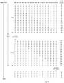
- the table of Figure 6 maps BTD_Lower outputs to respective sets of Q inputs for TBC 412.
- Figure 6 shows that BTD_Lower increases sequentially from 0 to 15 during the first half of the GRO cycle, and increases sequentially from 16 to 31 during the second half of the GRO cycle.
- Counter 414 is configured to count the number of completed GRO cycles.
- Counter 414 includes several inputs including INCRT, ENBL and CLR, which receive the output of AND gate 416, the output of flip-flop 422, and the Reset signal, respectively.
- AND gate 416 receives the output of buffer 402-15 and the output of inverter 420, which in turn receives UaD.
- Counter 414 must be enabled before it begins counting.
- ENBL of counter 414 is coupled to the output of flip-flop 422.
- the D input of flip-flop 422 is coupled to supply voltage VDD, and the clock input of flip-flop 422 is connected to the output of the inverter 424, which in turn receives the output of buffer 402-15.
- Counter 414 is enabled when the output of buffer 402-15 first transitions from high to low, which occurs at end of the first half of the initial GRO cycle as noted above. Counter 414, when enabled, will increment its counter value BTD_Upper each time N15 transitions from low to high (i.e., at the end of each second half cycle) until UaD is asserted high. Counter 414 will clear BTD _Upper when Reset is asserted high.
- TDC 116 includes a latch 430 that latches the value of BTD_Upper when the GRO is deactivated.
- Latch 430 includes separate inputs CLR and LTCH. The latch input LTCH receives UaD. Accordingly, latch 430 latches the BTD_Upper value of counter 414 when UaD goes high. Latch 430 will clear its stored content when Reset is asserted high.
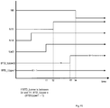
- FIG. 7 illustrates a timing diagram that shows oscillator signals near the end of a GRO cycle. In particular the figure shows: the state at nodes N14 and N15, which correspond to the outputs of buffers 402-14 and 402-15, respectively; UaD, and; the value of BTD _Upper of counter 414.
- relevant components of the TDC 116 are shown in Figure 7 .
- UaD goes high at time t1, which is just before the end of a GRO cycle (i.e., before N15 goes high at time t2).
- counter 414 should deactivate immediately when UaD goes high so that counter 414 does not increment BTD _Upper after N15 transitions to high at time t2.
- Further latch 430 should capture BTD_Upper immediately when UaD goes high. Due to signal delay, however, counter 414 may increment BTD_Upper from M to M+1 at time t3.
- latch 430 will capture BTD_Upper either at time t4, which is before BTD _Upper is incremented, or at time t5, which is after BTD _Upper is incremented. If latch 430 captures BTD _Upper at time t5, the resulting BTD value will be higher than it should be and thus a substantially inaccurate representation of ⁇ .
- Figure 8 is a timing chart that illustrates another example in which TDC 116 may generate an inaccurate representation of ⁇ .
- Figure 8 shows UaD signal going high at time t2, which is just after the end of a full GRO cycle (i.e., after N15 goes high at time t1). Due to signal delay, counter 414 may increment BTD_Upper from M to M+1 at time t3.
- Latch 430 will capture BTD_Upper either at time t4, which is before BTD_Upper is incremented, or at time t5, which is after BTD_Upper is incremented. If latch 430 captures BTD_Upper at time t4, the resulting BTD value will be lower than it should be and thus a substantially inaccurate representation of ⁇ .
- FIG. 9 is a block diagram illustrating an example PLL employing a PDC, which in turn employs a TDC according to one embodiment of the present disclosure.
- PLL 900 is similar to PLL 100 shown in Figure 1 in that they both contain digital filter 104, SDM 106, oscillator system 110, and feedback divider 112.
- PLL 900 includes PDC 902, which in turn includes PFD 114 and TDC 906.
- TDC 906 generates a binary time delay BTD for subsequent processing by digital filter 104.
- TDC 902 generates BTD in a substantially different manner.
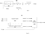
- TDC 906 includes a stopwatch system 1010 that concurrently provides a pair of BTD_Upper values (BTD_Upper1 and BTD_Upper2), and Q outputs (Q0 - Q15).
- stopwatch system 1010 includes an oscillator that generates a periodic signal when activated, and separate counters that increment BTD_Upper1 and BTD_Upper2 at different points in the cycle of the periodic signal. At each point in the cycle at least one of the two counter values will be stable or unaffected by signal transmission delay problems like those described above.
- TDC 906 selects a stable counter value to produce binary time delay BTD.
- TDC 906 includes TBC 412, which generates BTD_Lower as described above.
- TDC 906 also includes a BTD generator 1012 that generates BTD based on TD_Sign provided by PFD 114, BTD _Lower provided by TBC 412, and one of BTD_Upper1 and BTD_Upper2 provided by stopwatch system 1010.
- BTD generator 1012 selects one of BTD_Upper1 and BTD_Upper2 for use in generating BTD based upon BTD Lower.
- BTD generator 1012 generates BTD according to the following conditions:
- FIGS 11 and 12 illustrate alternative embodiments of BTD generator 1012. Each of these figures show stopwatch system 1010 in block diagram form, which generates BTD_Upper1 and BTD_Upper2. TBC 412 generates BTD _Lower based upon the Q0 - Q15 outputs of stopwatch system 1010.
- BTD generator 1012 includes a multiplexer 1102 that receives BTD_Upper1 and BTD_Upper2 from stopwatch system 1010. Additionally, multiplexer 1102 receives BTD_Upper1-1 from decrementor 1104. Decoder 1106 provides a select signal that is used by multiplexer 1102 to select one of the three inputs for output to combiner 1108.
- decoder 1106 decodes BTD _Lower to generate the select signal, which is set to: a first state if 0 ⁇ BTD _Lower ⁇ 7; a second state if 8 ⁇ BTD _Lower ⁇ 23, or; a third state if 24 ⁇ BTD _Lower ⁇ 31.
- Multiplexer 1102 outputs: BTD_Upper1 if the select signal is set to the first state; BTD_Upper2 if the select signal is set to the second state, or; BTD_Upper1 - 1 if the select signal is set to the third state.
- Combiner 1108 receives and combines TD_Sign, the output of multiplexer 1102, and BTD _Lower to generate BTD.
- BTD generator 1012 includes multiplexer 1202 that receives BTD_Upper1 and BTD_Upper2 from stopwatch system 1010. Decoder 1206 provides a select signal that is used by multiplexer 1202 to select one of the two inputs for output to decrementor 1204. Decoder 1206 decodes BTD_Lower to generate the select signal, which is set to: a first state if 0 ⁇ BTD_Lower ⁇ 7 or if 24 ⁇ BTD _Lower ⁇ 31, or; a second state if 8 ⁇ BTD _Lower ⁇ 23.
- Multiplexer 1202 outputs: BTD_Upper1 if the select signal is set to the first state, or; BTD_Upper2 if the select signal is set to the second state.
- Decoder 1206 generates a second signal based upon BTD_Lower, and this second signal is provided to decrementor 1204. Decrementor 1204 may or may not decrement the output of multiplexor 1202. When the second signal is asserted, decrementor 1204 decrements the value provided by multiplexer 1204. Otherwise, decrementor 1204 passes the value it receives from multiplexer 1202 to combiner 1210 without modification. In one embodiment, the second signal is asserted only when 24 ⁇ BTD _Lower ⁇ 31.
- Combiner 1210 receives and combines TD_Sign, the output of decrementor 1204, and BTD _Lower to generate BTD.
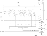
- FIG 13 illustrates relevant aspects of stopwatch system 1010, which includes many of the components shown within Figure 4 .
- stopwatch system 1010 includes the GRO of Figure 4 , which in turn includes fifteen non-inverting buffers 402 connected in a ring via NAND gate 404, which in turn receives the output of buffer 402-15 and UoD from the PFD 114 (not shown in Figure 13 ).
- the GRO When the GRO is activated by UoD, the GRO repeats a cycle in which each of nodes N0 - N15 oscillates between high and low values.
- Figure 14 illustrates the states of nodes N0 - N15 as the GRO undergoes a complete GRO cycle. Each full GRO cycle consists of a first half cycle followed by a second half cycle.
- stopwatch system 1010 includes first and second counters 1302 and 1304. Each of the counters will be enabled soon after the GRO is activated.
- first counter 1302 when enabled, will increment its counter value BTD_Upper1 at the end of each first half cycle
- second counter 1304 when enabled, will increment its counter value BTD_Upper2 at the end of each second half cycle.
- counters 1302 and 1304 can increment their respective counter values at different points in the GRO cycle in alternative embodiments.
- Counter 1302 includes several inputs including INCRT, ENBL and CLR, which receive the output signal of AND gate 1310, the Enable1 output signal of flip-flop 1312, and the Reset signal, respectively.
- the clock input of flip-flop 1312 receives the output of inverter 1318-1.
- Counter 1302 resets its counter value BTD_Upper1 to zero each time the Reset signal goes high.
- Counter 1302 is enabled when the Enable1 output of flip-flop 1312 goes high, which occurs the first time node N0 goes low.
- AND gate 1310 receives the output NAND gate 404 and the output of inverter 420, which in turn receives UaD. When enabled and while UaD is low, counter 1302 increments BTD_Upper1 each time the output N0 of NAND gate 404 transitions from low to high, which occurs at the end of each first half cycle as shown in Figure 14 .
- Counter 1304 includes the same inputs as counter 1302. INCRT, ENBL and CLR, receive the output signal of AND gate 1314, the Enable2 output signal of flip-flop 1316, and the Reset signal, respectively.
- the clock input of flip-flop 1316 receives the output of inverter 1318-2.
- Counter 1304 resets its counter value BTD_Upper2 to zero each time Reset is asserted.
- Counter 1304 is enabled when Enable2 goes high, which occurs the first time when node N15 goes low.
- Counter 1304 is enabled during the initial first half cycle of the GRO cycle.
- AND gate 1314 receives the output buffer 402-15 and the output of inverter 420, which in turn receives UaD.
- counter 1304 When enabled and while UaD is low, counter 1304 increments its counter value BTD_Upper2 each time the output N15 of buffer 402-15 transitions from low to high, which occurs at the end of each GRO cycle as shown in Figure 14 . Since N0 transitions to high before N15 transitions to high, counter 1302 increments before counter 1304 during each GRO cycle. Depending on when the GRO is deactivated, counter 1304 may not increment after counter 1302 increments. While counters 1302 and 1304 increment when NO and N15 transition, they can increment when different nodes transition in alternative embodiments. For example, inputs to AND gates 1310 and 1314 can be connected to nodes N1 and N14, respectively, which means counters 1302 and 1304 would increment with transitions at nodes N1 and N14, respectively.
- Stopwatch system 1010 includes flip-flops 410-0 - 410-15, which capture the voltage levels at nodes N0 - N15, respectively, when UaD transitions from low to high (i.e., when in the GRO is deactivated).
- the Q outputs of flip-flops 410-0 - 410-15 are provided as inputs to thermometric-to-binary converter (TBC) 412 for translation into BTD Lower.
- TBC thermometric-to-binary converter
- Stopwatch system 1010 also includes a pair of latches circuits 1306 and 1308, which receive the BTD_Upper1 and BTD_Upper2 values, respectively from counters 1302 and 1304, respectively.
- Counter latch 1306 includes a clear input CLR that receives Reset, and a latch input LTCH that receives UaD.
- Counter latch 1306 latches or captures the value of BTD_Upper1 when the GRO is deactivated (i.e., when UaD transitions from low to high).
- Counter latch 1308 includes a clear input CLR that receives Reset and a latch input LTCH that receives BTD_Upper2.
- Counter latch 1308 captures the value of BTD_Upper2 when the GRO is deactivated. Both latches 1306 and 1308 clear their captured values when Reset is asserted high.
- the accuracy of counter 1302 or 1304 may be susceptible to signal delay issues at various points in the GRO cycle. However, the accuracy of both will not be susceptible at the same time. In other words, at least one of BTD_Upper1 or BTD_Upper2 will be accurate or stable at all times during the GRO cycle. Based on the point in the cycle at which the GRO is deactivated, TDC 906 will select the stable value (i.e., BTD_Upper1 or BTD_Upper2) for subsequent use in generating BTD. Because BTD is generated with a stable BTD_Upper1 or BTD_Upper2, the BTD generated by TDC 906 is substantially insensitive to the signal delay issues described with reference to Figures 7 and 8 .
- BTD generator 1012 will generate an accurate BTD representation of phase delay ⁇ , regardless of the point during the full GRO cycle at which UaD transitions to high.
- Figure 15 is a diagram similar to that shown within Figure 7 and shows the levels of nodes N0, N14, and N15 near the end of a GRO cycle (i.e., when N15 transitions to high).
- UaD goes high at time t1, which is between the times at which nodes N14 and N15 go high.
- M not M+1, should be used to generate BTD since UaD goes high before the completion of the full GRO cycle.
- the resulting BTD will be a substantially accurate representation of ⁇ .
- FIG 16 shows another example in which an unstable value is avoided when generating BTD.
- BTD_Upper2 increments to M+1 at t4, which occurs after N15 transitions to high at t1 and after NO transitions to low at t2.
- BTW _Lower is properly 0 after UaD transitions to high at time t3.
- BTD_Upper2 is slow to increment due to signal delay.
- BTD_Upper2 is unstable just after UaD transitions to high (i.e., deactivation of the GRO).
- BTD_Upper2 should not be used to generate BTD.
- BRD_Lower1 is stable after time t3.
- the resulting BTD will be a substantially accurate representation of ⁇ .
- an apparatus in one embodiment, includes a phase to digital converter (PDC) configured to generate a digital output that represents a phase difference between first and second clocks.
- the PDC includes a gated ring oscillator (GRO), which includes N signal delay elements coupled together in a ring via a logic gate, wherein a 1st signal delay element of the ring comprises an input coupled to an output of the logic gate, and wherein a Nth signal delay element of the ring comprises an output coupled to a first input of the logic gate.
- GRO gated ring oscillator
- the apparatus also includes a convertor is coupled to the GRO and configured to generate low order bits of the digital output based on outputs of the logic gate and the N signal delay elements.
- the apparatus also includes a first counter includes an input coupled to an output of one of the N signal delay elements or the logic gate, wherein the first counter is configured to generate a first digital counter value.
- the apparatus also includes a second counter includes an input coupled to an output of another one of the N signal delay elements or the logic gate, wherein the second counter is configured to generate a second digital counter value.
- the PDC generates the digital output signal based on the low order bits and one of the first and second digital counter values.
- the PDC may further include a phase frequency detector (PFD), which includes a first output coupled to a second input of the logic gate, wherein the PFD is configured to start the GRO with a first edge of the first clock, and wherein the PFD is configured to stop the GRO with a first edge of the second clock.
- the input of the first counter may be coupled to the output of the logic gate, and the input of the second counter may be coupled to the output of the Nth signal delay element.
- the PDC may further include a multiplexor for selecting the first or second digital counter value based on the low order bits, wherein the PDC generates the digital output based on the first or second digital counter value selected by the multiplexor.
- the multiplexor may select the first digital counter value when the lower order bits represent a value that is contained in a range of values, and the multiplexor may select the second digital counter value when the lower order bits represent a value that is not contained in the range of values.
- the PDC may further include a combinational arithmetic circuit that decrements the first digital counter when selected by the multiplexor, and when the lower order bits represent a value that is contained in a second range of values, wherein the first and second range of values are non-overlapping.
- Each of the N signal delay elements may be a non-inverting buffer.
- the apparatus may further include a controlled oscillator configured to generate an output clock with a frequency that depends on the digital output of the PDC, and a feedback divider configured to generate the second clock based on the system clock.
- an apparatus in another embodiment, includes a gated ring oscillator (GRO), wherein the GRO includes N signal delay elements coupled together in a ring via a logic gate, wherein a 1st signal delay element of the ring includes an input coupled to an output of the logic gate, and wherein a Nth delay element of the ring comprises an output coupled to a first input of the logic gate.
- the apparatus also includes a GRO controller, wherein the GRO controller comprises a first output coupled to a second input of the logic gate, wherein the GRO controller is configured to activate the GRO in response to a first signal transitioning between first and second states, and wherein the GRO controller is configured to deactivate the GRO in response to a second signal transitioning between the first and second states.
- the apparatus also includes N+1 latches for latching respective outputs of the logic gate and the N signal delay elements in response to GRO controller deactivating the GRO.
- the apparatus also includes a first counter configured to increment a first counter value in response to an output of the one of the N+1 signal delay elements or the logic gate transitioning from the first state to the second state.
- the apparatus also includes a second counter configured to increment a second counter value in response to an output of another one of the N+1 signal delay elements or the logic gate transitioning from the first state to the second state.
- the apparatus also includes a circuit for generating a digital value that is proportional to a time difference between the activation and deactivation of the GRO, wherein the circuit generates the digital value based on outputs of the N+1 latches and one of the first and second counter values.
- the outputs of each of the N signal delay elements and the logic gate may oscillate between the first and second states while the gate GRO is activated.
- the input of the first counter may be coupled to the output of the logic gate, and the input of the second counter may be coupled to the output of the Nth signal delay element.
- the apparatus may further include a multiplexor for selecting the first or second digital counter value based on the low order bits, wherein the PDC generates the digital output based on the first or second counter value selected by the multiplexor.
- the multiplexor may select the first counter value when the lower order bits represent a value that is contained in a range of values, and wherein the multiplexor may select the second counter value when the lower order bits represent a value that is not contained in the range of values.
- the apparatus may further include a combinational arithmetic circuit that decrements the first counter when selected by the multiplexor, and when the lower order bits represent a value that is contained in a second range of values, wherein the first and second range of values are non-overlapping.
- an apparatus in still another embodiment, includes an oscillator that generates a periodic signal at an output when activated.
- the apparatus also includes first counter and second counters that increment first and second counter values, respectively, during each cycle of the periodic signal.
- the apparatus also includes a controller, wherein the controller is configured to activate the oscillator in response to a first signal transitioning between first and second states, and wherein the controller is configured to deactivate the oscillator in response to a second signal transitioning between the first and second states.
- the apparatus also includes a circuit for generating a first digital value that is proportional to a point in time in a cycle of the periodic signal when the second signal transitions between first and second states.
- the apparatus also includes a multiplexor for selecting the first counter value or the second counter value based on the first digital value.
- the apparatus also includes a circuit for generating a second digital value that represents a time difference between a time when the first signal transitions between first and second states and a point in time when the second signal transitions between first and second states, wherein the circuit generates the second digital signal based on the first digital signal and the first or second counter value selected by the multiplexor.
- the first counter may increment the first counter value before the second counter increments the second counter value.
- the first counter may increment the first counter value at a first point in time from the beginning of each cycle of the periodic signal, and wherein the second counter may increment the second counter value at a second point in time from the beginning of each cycle of the periodic signal.
- the oscillator may include N signal delay elements coupled together in a ring via a logic gate, wherein a 1 st signal delay element of the ring comprises an input coupled to an output of the logic gate, and wherein a Nth delay element of the ring comprises an output coupled to a first input of the logic gate, the first counter may include an input coupled to an output of one of the N signal delay elements or the logic gate, and the second counter may include an input coupled to an output of another one of the N signal delay elements or the logic gate.
- the input of the first counter may be coupled to the output of the logic gate, and the input of the second counter may be coupled to the output of the Nth signal delay element.
- the multiplexor may select the first counter value when the first digital value is contained in a range of values, and wherein the multiplexor may select the second counter value when the first digital value is not contained in the range of values.
- a phase to digital converter (PDC) generates a digital output that represents a phase difference between first and second clocks.
- the PDC includes a gated ring oscillator (GRO), which includes N signal delay elements coupled together in a ring via a logic gate, wherein a 1 st signal delay element of the ring comprises an input coupled to an output of the logic gate, and wherein a Nth signal delay element of the ring comprises an output coupled to a first input of the logic gate.
- GRO gated ring oscillator
- a convertor is coupled to the GRO and configured to generate low order bits of the digital output based on outputs of the logic gate and the N signal delay elements.
- a first counter includes an input coupled to an output of one of the N signal delay elements or the logic gate, wherein the first counter is configured to generate a first digital counter value.
- a second counter includes an input coupled to an output of another one of the N signal delay elements or the logic gate, wherein the second counter is configured to generate a second digital counter value.
- the PDC generates the digital output signal based on the low order bits and one of the first and second digital counter values.
Landscapes
- Physics & Mathematics (AREA)
- General Physics & Mathematics (AREA)
- Stabilization Of Oscillater, Synchronisation, Frequency Synthesizers (AREA)
Abstract
Description
- A phase-to-digital convertor, as its name implies, converts a phase difference between clock signals into a digital representation. Phase-to-digital convertors are employed in digital phase locked loops (PLL), which are electronic systems that generate an output clock with a frequency that is a multiple of the frequency of an externally provided reference clock. PLLs are typically used for computer clock synchronization, demodulation, frequency synthesis, etc.
- A typical PLL contains a phase frequency detector (PFD), a controlled oscillator and a feedback path that includes a feedback divider. The PFD receives two clock inputs; a feedback clock from the feedback divider, and a reference clock. A clock has two edges, a leading or rising edge at the start of the clock period and a negative or edge that marks the end of a half clock period. PFDs detect a phase difference or time delay between rising edges of the reference and feedback clocks. The phase difference, depending on whether it is positive, negative, or zero, determines whether the controlled oscillator increases, decreases, or maintains the frequency fout of the output clock it generates. The feedback divider is positioned in the feedback path between the controlled oscillator and the PFD. The feedback divider, also called a clock divider, receives the output clock, and generates the feedback clock with frequency ffb = fout/Nfb where Nfb is often an integer. If the phase of the reference and feedback clocks are kept in lock step, the reference and feedback clock frequencies should be the same.
- Digital PLLs are replacing analog PLLs in many applications. Digital PLLs often employ phase-to-digital convertors, which in turn employ time-to-digital convertor subsystems that convert a phase difference between reference and feedback clocks into a digital representation. Unfortunately, time-to-digital convertors can present new challenges to accurate operation of systems, including digital PLLs, in which they are employed.
- The present technology may be better understood, and its numerous objects, features, and advantages made apparent to those skilled in the art by referencing the accompanying drawings.
-
Figure 1 is a block diagram of a PLL that includes a phase-to-digital converter. -
Figure 2 is a schematic diagram illustrating an example phase-frequency detector employed in the PLL ofFigure 1 . -
Figure 3 is a timing diagram illustrating operational aspects of the phase-frequency detector. -
Figure 4 is a diagram illustrating an example time-to-digital converter employed in PLL ofFigure 1 . -
Figure 5 illustrates the states of nodes of the oscillator shown inFigure 4 during a cycle thereof. -
Figure 6 is a table that shows the outputs of an example thermometric-to-binary converter for respective inputs. -
Figure 7 is a timing diagram illustrating adverse effects of time delay to the operation of the time-to-digital converter shown inFigure 4 . -
Figure 8 is another timing diagram illustrating adverse effects of time delay to the operation of the time-to-digital converter shown inFigure 4 . -
Figure 9 is a block diagram illustrating a PLL employing a phase-to-digital converter, which in turn employs a time-to-digital converter according to one embodiment of the present disclosure. -
Figure 10 is a block diagram illustrating an example time-to-digital converter according to one embodiment of the present disclosure. -
Figure 11 is a block diagram illustrating an example binary-time-delay generator employed in the time-to-digital converter ofFigure 10 . -
Figure 12 is a block diagram illustrating another example of a binary-time-delay generator employed in the time-to-digital converter ofFigure 10 . -
Figure 13 is a schematic diagram of an example stopwatch system employed in the time-to-digital converter ofFigure 11 . -
Figure 14 illustrates the states of nodes of the oscillator shown inFigure 13 during a cycle thereof. -
Figure 15 is a timing diagram illustrating example operational aspects of the present disclosure. - The use of the same reference symbols in different drawings indicates similar or identical items.
- Phase-to-digital convertors generate a digital signal that is proportional to a phase difference between a pair of clock signals. The accuracy of a phase-to-digital convertor can be subject to unexpectedly short or unexpectedly long signal transmission delay within the converter. Disclosed is a phase-to-digital convertor whose accuracy is less sensitive to signal transmission delay. The phase-to-digital convertor of the present disclosure employs a time-to-digital convertor, which includes a subsystem (referred to as the "stopwatch system") that includes an oscillator and at least two counters. The oscillator generates a periodic signal when activated by the rising edge of a first clock. The counters increment their respective counter values at different points during each cycle of the oscillator's periodic signal. When the oscillator is deactivated by the rising edge of a second clock, the phase-to-digital convertor selects one of the counter values based on the point during the last periodic cycle when the oscillator was deactivated. The phase-to-digital convertor uses the selected counter value to generate a digital representation of a phase difference between the first and second clocks. The phase-to-digital convertor of the present disclosure will be described with reference to use within a PLL, it being understood the present disclosure should not be limited thereto.
- As noted above, the accuracy of phase-to-digital convertors can be sensitive to signal transmission delay.
Figures 1-8 illustrate this problem in greater detail.Figure 1 is a block diagram of asimple PLL 100 that includes a phase-to-digital convertor (PDC) 102.PLL 100 generates an output clock OCLK that tracks an externally provided reference clock RCLK. PDC 102 receives and compares the rising edges of the reference clock RCLK and a feedback clock FBCLK output offeedback divider 112.PDC 102 generates a multi-bit digital value indicative of a phase difference or time delay between the two input clocks. The multi-bit digital value will be referred to herein as the binary time delay (BTD) value. -
Digital filter 104, which in one embodiment is a narrowband device, filters BTD, the result of which is subsequently processed by sigma delta modulator (SDM) 106. A controlledoscillator system 110 generates an output clock OCLK, the frequency fout of which depends on the output ofSDM 106. The output clock OCLK is provided tofeedback divider 112, which in turn provides feedback clock FBCLK toPDC 102 with frequency ffb = fout/Nfb. -
PDC 102 includes a phase frequency detector (PFD) 114 and time-to-digital converter (TDC) 116.PFD 114 detects the phase or time delay between the reference clock RCLK and the feedback clock FBCLK.PFD 114 also determines whether the reference clock RCLK is leading or lagging. TDC 116 translates this information into the multibit BTD value that represents the magnitude and sign (e.g., leading or lagging) of the phase difference. - An
example PFD 114 is shown in the schematic diagram ofFigure 2 . PFD 114 includes a pair of input D flip-flops flop 202 receives reference clock RCLK at its clock input, and flip-flop 204 receives feedback clock FBCLK at its clock input. The D inputs of flip-flops flop 202 is designated as the up signal UP, while the Q output of D flip-flop 204 is designated as the down signal DOWN. After flip-flops gate 206 and ORgate 208 as shown. The output ofAND gate 206 is designated as the up and down signal UaD, while the output of ORgate 208 is designated as the up or down signal UoD. The clear-inputs of D flip-flops gate 206 viasignal delay 210 andOR gate 212, which also receives the Reset signal. Accordingly, the UP and DOWN outputs of D flip-flops Figure 2 the clock input of D flip-flop 214 receives the UP signal, and the D input of flip D flip-flop 214 receives the DOWN signal. If feedback clock FBCLK leads reference clock RCLK, the output of flip-flop 214, which is designated as TD_Sign, will go high, and vice versa. Likeflip flops flop 214 is cleared by Reset, which can be asserted between cycles of the reference clock RCLK. - The operation of
PFD 114 can best be understood with reference to the timing diagram shown withinFigure 3 , which shows reference clock RCLK leading feedback clock FBCLK by phase difference ΦΔ. The UP signal output of flip-flop 202 transitions to high at theleading edge 302 of reference clock RCLK. This in turn causes the UoD output of ORgate 208 to go high. Although not shown inFigure 3 , TD_Sign output of flip-flop 214 stays low at the transition of the UP signal, thus indicating that reference clock RCLK leads the feedback clock FBCLK. The DOWN signal output of flip-flop 204 transitions to high at theleading edge 304 of feedback clock FBCLK. With both UP and DOWN asserted high, UaD goes high. ΦΔ is represented by the time difference between UoD and UaD as shown. After a delay introduced by delay element 210 (and to a lesser extent by OR gate 212), asserted UaD causes the UP and DOWN outputs of flip-flops gate 208 and ANDgate 206, respectively, to go low. - With continuing reference to
Figures 1 - 3 ,Figure 4 illustratesTDC 116, which generates a multibit binary time delay BTD value that represents the phase difference ΦΔ between reference clock RCLK and feedback clock FBCLK. As will be more fully described, BTD is generated by concatenating three values; TD_Sign, BTD_Upper, and BTD_Lower. -
TDC 116 includes an example gated ring oscillator (GRO), which in turn includes signal delay elements 402 connected in a ring as shown viaNAND gate 404. The delay elements 402 take form in noninverting buffers, it being understood alternative delay elements are contemplated. The output of buffer 402-15 is fed back to the input ofNAND gate 404 viafeedback path 406.NAND gate 404 also receives UoD from PFD 114 (not shown inFigure 4 ). The outputs ofNAND gate 404 and buffers 402, which are designated as nodes NO - N15 of the GRO, are at a high voltage level prior to GRO activation. - The GRO is activated when UoD goes high. When activated, the GRO repeats a cycle.
Figure 5 illustrates the states of nodes N0 - N15 shown inFigure 4 as the GRO undergoes a cycle. The GRO cycle consists of a first half cycle followed by a second half cycle as shown inFigure 5 . - With continuing reference to
Figures 4 and5 , when UoD transitions to high, node N0 goes low, and this low voltage level propagates sequentially through buffers 402 during the first half of the GRO cycle, which ends when all of nodes N0 - N15 are low. And the second half of the GRO cycle starts after node N15 transitions to low. Because the output of buffer 402-15 is fed back to an input ofNAND gate 404, node N0 goes high in response to N15 going low. And this high level propagates sequentially through buffers 402. The GRO cycle ends, and the next begins after the output (i.e., node N15) of buffer 402-15 transitions back to high. It is noted the GRO cycle repeats while UoD is high. -
TDC 116 includes D flip-flops 410 that capture the state of the GRO immediately when the GRO is deactivated. In other words, flip-flops 410-0 - 410-15 capture the voltage levels at nodes N0 - N15, respectively, when UaD transitions from low to high. The Q outputs of flip-flops 410-0 - 410-15 are collectively provided as an input to thermometric-to-binary converter (TBC) 412 for translation into BTD_Lower. The table ofFigure 6 maps BTD_Lower outputs to respective sets of Q inputs forTBC 412.Figure 6 shows that BTD_Lower increases sequentially from 0 to 15 during the first half of the GRO cycle, and increases sequentially from 16 to 31 during the second half of the GRO cycle. -
Counter 414 is configured to count the number of completed GRO cycles.Counter 414 includes several inputs including INCRT, ENBL and CLR, which receive the output of ANDgate 416, the output of flip-flop 422, and the Reset signal, respectively. ANDgate 416 receives the output of buffer 402-15 and the output ofinverter 420, which in turn receives UaD.Counter 414 must be enabled before it begins counting. ENBL ofcounter 414 is coupled to the output of flip-flop 422. The D input of flip-flop 422 is coupled to supply voltage VDD, and the clock input of flip-flop 422 is connected to the output of theinverter 424, which in turn receives the output of buffer 402-15.Counter 414 is enabled when the output of buffer 402-15 first transitions from high to low, which occurs at end of the first half of the initial GRO cycle as noted above.Counter 414, when enabled, will increment its counter value BTD_Upper each time N15 transitions from low to high (i.e., at the end of each second half cycle) until UaD is asserted high.Counter 414 will clear BTD _Upper when Reset is asserted high. -
TDC 116 includes alatch 430 that latches the value of BTD_Upper when the GRO is deactivated.Latch 430 includes separate inputs CLR and LTCH. The latch input LTCH receives UaD. Accordingly, latch 430 latches the BTD_Upper value ofcounter 414 when UaD goes high.Latch 430 will clear its stored content when Reset is asserted high. -
Combiner 432, as its name implies, combines or concatenates the time delay signal TD_Sign, the latched BTD_Upper value provided by thelatch 430, and the BTD_Lower value provided byTBC 412, to create BTD. In other words,combiner 432 generates BTD = TD_Sign|| BTD_Upper||BTD_Lower. - Most of the time the BTD value output of
TDC 116 is a substantially accurate digital representation of the phase delay ΦΔ. Unfortunately, under somecircumstances TDC 116 may generate a less than accurate BTD value. For example,TDC 116 may not produce an accurate BTD when the GRO is deactivated (i.e., when UaD transitions to high) near the end of a GRO cycle. To illustrate,Figure 7 illustrates a timing diagram that shows oscillator signals near the end of a GRO cycle. In particular the figure shows: the state at nodes N14 and N15, which correspond to the outputs of buffers 402-14 and 402-15, respectively; UaD, and; the value of BTD _Upper ofcounter 414. For convenience, relevant components of theTDC 116 are shown inFigure 7 . - UaD goes high at time t1, which is just before the end of a GRO cycle (i.e., before N15 goes high at time t2). Ideally, counter 414 should deactivate immediately when UaD goes high so that
counter 414 does not increment BTD _Upper after N15 transitions to high at time t2.Further latch 430 should capture BTD_Upper immediately when UaD goes high. Due to signal delay, however, counter 414 may increment BTD_Upper from M to M+1 at time t3. Depending on signal delay, latch 430 will capture BTD_Upper either at time t4, which is before BTD _Upper is incremented, or at time t5, which is after BTD _Upper is incremented. Iflatch 430 captures BTD _Upper at time t5, the resulting BTD value will be higher than it should be and thus a substantially inaccurate representation of ΦΔ. -
Figure 8 is a timing chart that illustrates another example in whichTDC 116 may generate an inaccurate representation of ΦΔ.Figure 8 shows UaD signal going high at time t2, which is just after the end of a full GRO cycle (i.e., after N15 goes high at time t1). Due to signal delay, counter 414 may increment BTD_Upper from M to M+1 at time t3.Latch 430 will capture BTD_Upper either at time t4, which is before BTD_Upper is incremented, or at time t5, which is after BTD_Upper is incremented. Iflatch 430 captures BTD_Upper at time t4, the resulting BTD value will be lower than it should be and thus a substantially inaccurate representation of ΦΔ. - The present disclosure provides a TDC that is substantially more accurate when compared to
TDC 116.Figure 9 is a block diagram illustrating an example PLL employing a PDC, which in turn employs a TDC according to one embodiment of the present disclosure.PLL 900 is similar toPLL 100 shown inFigure 1 in that they both containdigital filter 104,SDM 106,oscillator system 110, andfeedback divider 112.PLL 900 includesPDC 902, which in turn includesPFD 114 andTDC 906. LikeTDC 116,TDC 906 generates a binary time delay BTD for subsequent processing bydigital filter 104. However,TDC 902 generates BTD in a substantially different manner. - An
example TDC 906 is shown inFigure 10 .TDC 906 includes astopwatch system 1010 that concurrently provides a pair of BTD_Upper values (BTD_Upper1 and BTD_Upper2), and Q outputs (Q0 - Q15). As will be shown in later figures,stopwatch system 1010 includes an oscillator that generates a periodic signal when activated, and separate counters that increment BTD_Upper1 and BTD_Upper2 at different points in the cycle of the periodic signal. At each point in the cycle at least one of the two counter values will be stable or unaffected by signal transmission delay problems like those described above.TDC 906 selects a stable counter value to produce binary time delay BTD. -
TDC 906 includesTBC 412, which generates BTD_Lower as described above.TDC 906 also includes aBTD generator 1012 that generates BTD based on TD_Sign provided byPFD 114, BTD _Lower provided byTBC 412, and one of BTD_Upper1 and BTD_Upper2 provided bystopwatch system 1010.BTD generator 1012 selects one of BTD_Upper1 and BTD_Upper2 for use in generating BTD based upon BTD Lower. In one embodiment,BTD generator 1012 generates BTD according to the following conditions: - If BTD Lower is 0 - 7, then BTD = TD_Sign||BTD_Upper1||BTD_Lower
- If BTD Lower is 8 - 23, then BTD = TD_Sign||BTD_Upper2||BTD_Lower
- If BTD_Lower is 24 - 31, then BTD = TD_Sign||(BTD_Upper1-1)||BTD_Lower
-
Figures 11 and12 illustrate alternative embodiments ofBTD generator 1012. Each of these figures showstopwatch system 1010 in block diagram form, which generates BTD_Upper1 and BTD_Upper2.TBC 412 generates BTD _Lower based upon the Q0 - Q15 outputs ofstopwatch system 1010. InFigure 11 ,BTD generator 1012 includes amultiplexer 1102 that receives BTD_Upper1 and BTD_Upper2 fromstopwatch system 1010. Additionally,multiplexer 1102 receives BTD_Upper1-1 fromdecrementor 1104.Decoder 1106 provides a select signal that is used bymultiplexer 1102 to select one of the three inputs for output tocombiner 1108. In the disclosedembodiment decoder 1106 decodes BTD _Lower to generate the select signal, which is set to: a first state if 0 ≤ BTD _Lower ≤ 7; a second state if 8 ≤ BTD _Lower ≤ 23, or; a third state if 24 ≤ BTD _Lower ≤ 31. Multiplexer 1102 outputs: BTD_Upper1 if the select signal is set to the first state; BTD_Upper2 if the select signal is set to the second state, or; BTD_Upper1 - 1 if the select signal is set to the third state.Combiner 1108 receives and combines TD_Sign, the output ofmultiplexer 1102, and BTD _Lower to generate BTD. - In
Figure 12 BTD generator 1012 includesmultiplexer 1202 that receives BTD_Upper1 and BTD_Upper2 fromstopwatch system 1010.Decoder 1206 provides a select signal that is used bymultiplexer 1202 to select one of the two inputs for output todecrementor 1204.Decoder 1206 decodes BTD_Lower to generate the select signal, which is set to: a first state if 0 ≤ BTD_Lower ≤ 7 or if 24 ≤ BTD _Lower ≤ 31, or; a second state if 8 ≤ BTD _Lower ≤ 23. Multiplexer 1202 outputs: BTD_Upper1 if the select signal is set to the first state, or; BTD_Upper2 if the select signal is set to the second state.Decoder 1206 generates a second signal based upon BTD_Lower, and this second signal is provided todecrementor 1204.Decrementor 1204 may or may not decrement the output ofmultiplexor 1202. When the second signal is asserted,decrementor 1204 decrements the value provided bymultiplexer 1204. Otherwise, decrementor 1204 passes the value it receives frommultiplexer 1202 tocombiner 1210 without modification. In one embodiment, the second signal is asserted only when 24 ≤ BTD _Lower ≤ 31.Combiner 1210 receives and combines TD_Sign, the output ofdecrementor 1204, and BTD _Lower to generate BTD. -
Figure 13 illustrates relevant aspects ofstopwatch system 1010, which includes many of the components shown withinFigure 4 . For example,stopwatch system 1010 includes the GRO ofFigure 4 , which in turn includes fifteen non-inverting buffers 402 connected in a ring viaNAND gate 404, which in turn receives the output of buffer 402-15 and UoD from the PFD 114 (not shown inFigure 13 ). When the GRO is activated by UoD, the GRO repeats a cycle in which each of nodes N0 - N15 oscillates between high and low values.Figure 14 illustrates the states of nodes N0 - N15 as the GRO undergoes a complete GRO cycle. Each full GRO cycle consists of a first half cycle followed by a second half cycle. - With continuing reference to
Figures 13 and14 ,stopwatch system 1010 includes first andsecond counters first counter 1302, when enabled, will increment its counter value BTD_Upper1 at the end of each first half cycle, andsecond counter 1304, when enabled, will increment its counter value BTD_Upper2 at the end of each second half cycle. It should be noted that counters 1302 and 1304 can increment their respective counter values at different points in the GRO cycle in alternative embodiments. -
Counter 1302 includes several inputs including INCRT, ENBL and CLR, which receive the output signal of ANDgate 1310, the Enable1 output signal of flip-flop 1312, and the Reset signal, respectively. The clock input of flip-flop 1312 receives the output of inverter 1318-1.Counter 1302 resets its counter value BTD_Upper1 to zero each time the Reset signal goes high.Counter 1302 is enabled when the Enable1 output of flip-flop 1312 goes high, which occurs the first time node N0 goes low. ANDgate 1310 receives theoutput NAND gate 404 and the output ofinverter 420, which in turn receives UaD. When enabled and while UaD is low,counter 1302 increments BTD_Upper1 each time the output N0 ofNAND gate 404 transitions from low to high, which occurs at the end of each first half cycle as shown inFigure 14 . -
Counter 1304 includes the same inputs ascounter 1302. INCRT, ENBL and CLR, receive the output signal of ANDgate 1314, the Enable2 output signal of flip-flop 1316, and the Reset signal, respectively. The clock input of flip-flop 1316 receives the output of inverter 1318-2.Counter 1304 resets its counter value BTD_Upper2 to zero each time Reset is asserted.Counter 1304 is enabled when Enable2 goes high, which occurs the first time when node N15 goes low.Counter 1304 is enabled during the initial first half cycle of the GRO cycle. ANDgate 1314 receives the output buffer 402-15 and the output ofinverter 420, which in turn receives UaD. When enabled and while UaD is low,counter 1304 increments its counter value BTD_Upper2 each time the output N15 of buffer 402-15 transitions from low to high, which occurs at the end of each GRO cycle as shown inFigure 14 . Since N0 transitions to high before N15 transitions to high,counter 1302 increments beforecounter 1304 during each GRO cycle. Depending on when the GRO is deactivated,counter 1304 may not increment aftercounter 1302 increments. Whilecounters gates counters -
Stopwatch system 1010 includes flip-flops 410-0 - 410-15, which capture the voltage levels at nodes N0 - N15, respectively, when UaD transitions from low to high (i.e., when in the GRO is deactivated). The Q outputs of flip-flops 410-0 - 410-15 are provided as inputs to thermometric-to-binary converter (TBC) 412 for translation into BTD Lower. -
Stopwatch system 1010 also includes a pair oflatches circuits counters Counter latch 1306 includes a clear input CLR that receives Reset, and a latch input LTCH that receives UaD.Counter latch 1306 latches or captures the value of BTD_Upper1 when the GRO is deactivated (i.e., when UaD transitions from low to high).Counter latch 1308 includes a clear input CLR that receives Reset and a latch input LTCH that receives BTD_Upper2.Counter latch 1308 captures the value of BTD_Upper2 when the GRO is deactivated. Both latches 1306 and 1308 clear their captured values when Reset is asserted high. - The accuracy of
counter TDC 906 will select the stable value (i.e., BTD_Upper1 or BTD_Upper2) for subsequent use in generating BTD. Because BTD is generated with a stable BTD_Upper1 or BTD_Upper2, the BTD generated byTDC 906 is substantially insensitive to the signal delay issues described with reference toFigures 7 and8 . In other words,BTD generator 1012 will generate an accurate BTD representation of phase delay ΦΔ, regardless of the point during the full GRO cycle at which UaD transitions to high. To illustrate,Figure 15 is a diagram similar to that shown withinFigure 7 and shows the levels of nodes N0, N14, and N15 near the end of a GRO cycle (i.e., when N15 transitions to high). With continuing reference toFigures 10 - 14 , UaD goes high at time t1, which is between the times at which nodes N14 and N15 go high. One of ordinary skill understands that M, not M+1, should be used to generate BTD since UaD goes high before the completion of the full GRO cycle. Due to signal delay BTD_Upper2 increments to M+1 at time t3, which is shortly after t2, the time at which N15 goes high. BTD_Upper1 will not increment between times t1 and t4.Latches Latch 1308 will capture either BTD_Upper2=M or BTD_Upper2=M+1 depending upon whetherlatch 1308 completes its latching operation before or after BTD_Upper2 increments to M+1. Due to the uncertainty of whenlatch 1308 captures BTD_Upper2, the value captured bylatch 1308 should not be used to generate BTD. However,latch 1306 will capture BTD_Upper1=M+1 regardless of whetherlatch 1306 completes its operation before or after time t3. The value for BTD _Lower is most probably 30 or 31, and as aresult BTD generator 1012 selects BTD_Upper1-1 = M, for use in generating BTD. The resulting BTD will be a substantially accurate representation of ΦΔ. -
Figure 16 shows another example in which an unstable value is avoided when generating BTD. InFigure 16 BTD_Upper2 increments to M+1 at t4, which occurs after N15 transitions to high at t1 and after NO transitions to low at t2. BTW _Lower is properly 0 after UaD transitions to high at time t3. BTD_Upper2 is slow to increment due to signal delay. As a result, BTD_Upper2 is unstable just after UaD transitions to high (i.e., deactivation of the GRO). BTD_Upper2 should not be used to generate BTD. Fortunately, BRD_Lower1 is stable after time t3. The value for BTD_Lower is most probably 0 or 2, and as aresult BTD generator 1012 selects BTD_Upper1 = M+1, for use in generating BTD. The resulting BTD will be a substantially accurate representation of ΦΔ. - The following are various embodiments of the present disclosure. In one embodiment, an apparatus includes a phase to digital converter (PDC) configured to generate a digital output that represents a phase difference between first and second clocks. The PDC includes a gated ring oscillator (GRO), which includes N signal delay elements coupled together in a ring via a logic gate, wherein a 1st signal delay element of the ring comprises an input coupled to an output of the logic gate, and wherein a Nth signal delay element of the ring comprises an output coupled to a first input of the logic gate. The apparatus also includes a convertor is coupled to the GRO and configured to generate low order bits of the digital output based on outputs of the logic gate and the N signal delay elements. The apparatus also includes a first counter includes an input coupled to an output of one of the N signal delay elements or the logic gate, wherein the first counter is configured to generate a first digital counter value. The apparatus also includes a second counter includes an input coupled to an output of another one of the N signal delay elements or the logic gate, wherein the second counter is configured to generate a second digital counter value. The PDC generates the digital output signal based on the low order bits and one of the first and second digital counter values. The PDC may further include a phase frequency detector (PFD), which includes a first output coupled to a second input of the logic gate, wherein the PFD is configured to start the GRO with a first edge of the first clock, and wherein the PFD is configured to stop the GRO with a first edge of the second clock. The input of the first counter may be coupled to the output of the logic gate, and the input of the second counter may be coupled to the output of the Nth signal delay element. The PDC may further include a multiplexor for selecting the first or second digital counter value based on the low order bits, wherein the PDC generates the digital output based on the first or second digital counter value selected by the multiplexor. The multiplexor may select the first digital counter value when the lower order bits represent a value that is contained in a range of values, and the multiplexor may select the second digital counter value when the lower order bits represent a value that is not contained in the range of values. The PDC may further include a combinational arithmetic circuit that decrements the first digital counter when selected by the multiplexor, and when the lower order bits represent a value that is contained in a second range of values, wherein the first and second range of values are non-overlapping. Each of the N signal delay elements may be a non-inverting buffer. The apparatus may further include a controlled oscillator configured to generate an output clock with a frequency that depends on the digital output of the PDC, and a feedback divider configured to generate the second clock based on the system clock.
- In another embodiment, an apparatus includes a gated ring oscillator (GRO), wherein the GRO includes N signal delay elements coupled together in a ring via a logic gate, wherein a 1st signal delay element of the ring includes an input coupled to an output of the logic gate, and wherein a Nth delay element of the ring comprises an output coupled to a first input of the logic gate. The apparatus also includes a GRO controller, wherein the GRO controller comprises a first output coupled to a second input of the logic gate, wherein the GRO controller is configured to activate the GRO in response to a first signal transitioning between first and second states, and wherein the GRO controller is configured to deactivate the GRO in response to a second signal transitioning between the first and second states. The apparatus also includes N+1 latches for latching respective outputs of the logic gate and the N signal delay elements in response to GRO controller deactivating the GRO. The apparatus also includes a first counter configured to increment a first counter value in response to an output of the one of the N+1 signal delay elements or the logic gate transitioning from the first state to the second state. The apparatus also includes a second counter configured to increment a second counter value in response to an output of another one of the N+1 signal delay elements or the logic gate transitioning from the first state to the second state. The apparatus also includes a circuit for generating a digital value that is proportional to a time difference between the activation and deactivation of the GRO, wherein the circuit generates the digital value based on outputs of the N+1 latches and one of the first and second counter values. The outputs of each of the N signal delay elements and the logic gate may oscillate between the first and second states while the gate GRO is activated. The input of the first counter may be coupled to the output of the logic gate, and the input of the second counter may be coupled to the output of the Nth signal delay element. The apparatus may further include a multiplexor for selecting the first or second digital counter value based on the low order bits, wherein the PDC generates the digital output based on the first or second counter value selected by the multiplexor. The multiplexor may select the first counter value when the lower order bits represent a value that is contained in a range of values, and wherein the multiplexor may select the second counter value when the lower order bits represent a value that is not contained in the range of values. The apparatus may further include a combinational arithmetic circuit that decrements the first counter when selected by the multiplexor, and when the lower order bits represent a value that is contained in a second range of values, wherein the first and second range of values are non-overlapping.
- In still another embodiment, an apparatus includes an oscillator that generates a periodic signal at an output when activated. The apparatus also includes first counter and second counters that increment first and second counter values, respectively, during each cycle of the periodic signal. The apparatus also includes a controller, wherein the controller is configured to activate the oscillator in response to a first signal transitioning between first and second states, and wherein the controller is configured to deactivate the oscillator in response to a second signal transitioning between the first and second states. The apparatus also includes a circuit for generating a first digital value that is proportional to a point in time in a cycle of the periodic signal when the second signal transitions between first and second states. The apparatus also includes a multiplexor for selecting the first counter value or the second counter value based on the first digital value. The apparatus also includes a circuit for generating a second digital value that represents a time difference between a time when the first signal transitions between first and second states and a point in time when the second signal transitions between first and second states, wherein the circuit generates the second digital signal based on the first digital signal and the first or second counter value selected by the multiplexor. The first counter may increment the first counter value before the second counter increments the second counter value. The first counter may increment the first counter value at a first point in time from the beginning of each cycle of the periodic signal, and wherein the second counter may increment the second counter value at a second point in time from the beginning of each cycle of the periodic signal. The oscillator may include N signal delay elements coupled together in a ring via a logic gate, wherein a 1 st signal delay element of the ring comprises an input coupled to an output of the logic gate, and wherein a Nth delay element of the ring comprises an output coupled to a first input of the logic gate, the first counter may include an input coupled to an output of one of the N signal delay elements or the logic gate, and the second counter may include an input coupled to an output of another one of the N signal delay elements or the logic gate. The input of the first counter may be coupled to the output of the logic gate, and the input of the second counter may be coupled to the output of the Nth signal delay element. The multiplexor may select the first counter value when the first digital value is contained in a range of values, and wherein the multiplexor may select the second counter value when the first digital value is not contained in the range of values.
A phase to digital converter (PDC) generates a digital output that represents a phase difference between first and second clocks. The PDC includes a gated ring oscillator (GRO), which includes N signal delay elements coupled together in a ring via a logic gate, wherein a 1 st signal delay element of the ring comprises an input coupled to an output of the logic gate, and wherein a Nth signal delay element of the ring comprises an output coupled to a first input of the logic gate. A convertor is coupled to the GRO and configured to generate low order bits of the digital output based on outputs of the logic gate and the N signal delay elements. A first counter includes an input coupled to an output of one of the N signal delay elements or the logic gate, wherein the first counter is configured to generate a first digital counter value. A second counter includes an input coupled to an output of another one of the N signal delay elements or the logic gate, wherein the second counter is configured to generate a second digital counter value. The PDC generates the digital output signal based on the low order bits and one of the first and second digital counter values. - Although the present invention has been described in connection with several embodiments, the invention is not intended to be limited to the specific forms set forth herein. On the contrary, it is intended to cover such alternatives, modifications, and equivalents as can be reasonably included within the scope of the invention as defined by the appended claims.
Claims (8)
- An apparatus comprising:a phase to digital converter (PDC) configured to generate a digital output that represents a phase difference between first and second clocks, the PDC comprising:a gated ring oscillator (GRO), wherein the GRO comprises N signal delay elements coupled together in a ring via a logic gate, wherein a 1st signal delay element of the ring comprises an input coupled to an output of the logic gate, and wherein a Nth signal delay element of the ring comprises an output coupled to a first input of the logic gate;a convertor coupled to the GRO and configured to generate low order bits of the digital output based on outputs of the logic gate and the N signal delay elements;a first counter comprising an input coupled to an output of one of the N signal delay elements or the logic gate, wherein the first counter is configured to generate a first digital counter value;a second counter comprising an input coupled to an output of another one of the N signal delay elements or the logic gate, wherein the second counter is configured to generate a second digital counter value;wherein the PDC generates the digital output signal based on the low order bits and one of the first and second digital counter values.
- The apparatus of claim 1 wherein the PDC further comprises a phase frequency detector (PFD) comprising a first output coupled to a second input of the logic gate, wherein the PFD is configured to start the GRO with a first edge of the first clock, and wherein the PFD is configured to stop the GRO with a first edge of the second clock.
- The apparatus of claim 1 or 2 wherein the input of the first counter is coupled to the output of the logic gate, and the input of the second counter is coupled to the output of the Nth signal delay element.
- The apparatus of any preceding claim wherein the PDC further comprises a multiplexor for selecting the first or second digital counter value based on the low order bits, wherein the PDC generates the digital output based on the first or second digital counter value selected by the multiplexor.
- The apparatus of claim 4 wherein the multiplexor selects the first digital counter value when the lower order bits represent a value that is contained in a range of values, and wherein the multiplexor selects the second digital counter value when the lower order bits represent a value that is not contained in the range of values.
- The apparatus of claim 4 or 5 wherein the PDC further comprises a combinational arithmetic circuit that decrements the first digital counter when selected by the multiplexor, and when the lower order bits represent a value that is contained in a second range of values, wherein the first and second range of values are non-overlapping.
- The apparatus of any preceding claim wherein each of the N signal delay elements is a non-inverting buffer.
- The apparatus of any preceding claim further comprising:a controlled oscillator configured to generate an output clock with a frequency that depends on the digital output of the PDC;a feedback divider configured to generate the second clock based on the system clock.
Applications Claiming Priority (1)
| Application Number | Priority Date | Filing Date | Title |
|---|---|---|---|
| US16/580,117 US10819355B1 (en) | 2019-09-24 | 2019-09-24 | Phase to digital converter |
Publications (2)
| Publication Number | Publication Date |
|---|---|
| EP3799312A1 true EP3799312A1 (en) | 2021-03-31 |
| EP3799312B1 EP3799312B1 (en) | 2025-04-09 |
Family
ID=72193391
Family Applications (1)
| Application Number | Title | Priority Date | Filing Date |
|---|---|---|---|
| EP20192249.9A Active EP3799312B1 (en) | 2019-09-24 | 2020-08-21 | Phase to digital converter |
Country Status (2)
| Country | Link |
|---|---|
| US (1) | US10819355B1 (en) |
| EP (1) | EP3799312B1 (en) |
Families Citing this family (6)
| Publication number | Priority date | Publication date | Assignee | Title |
|---|---|---|---|---|
| CN111433686B (en) * | 2017-12-14 | 2021-09-14 | 华为国际有限公司 | Time-to-digital converter |
| CN111654281B (en) * | 2020-06-10 | 2023-08-04 | 上海兆芯集成电路股份有限公司 | time converter |
| US11533058B2 (en) * | 2020-12-17 | 2022-12-20 | Qualcomm Incorporated | Digital phase-frequency detector with split control loops for low jitter and fast locking |
| US11736110B2 (en) * | 2021-09-30 | 2023-08-22 | Shaoxing Yuanfang Semiconductor Co., Ltd. | Time-to-digital converter (TDC) to operate with input clock signals with jitter |
| CN114675525B (en) * | 2021-09-30 | 2022-09-02 | 绍兴圆方半导体有限公司 | Time-to-digital converter and clock synchronization system |
| US11592786B1 (en) * | 2022-05-10 | 2023-02-28 | Shaoxing Yuanfang Semiconductor Co., Ltd. | Time-to-digital converter (TDC) measuring phase difference between periodic inputs |
Citations (3)
| Publication number | Priority date | Publication date | Assignee | Title |
|---|---|---|---|---|
| US5416444A (en) * | 1993-01-14 | 1995-05-16 | Nippondenso Co., Ltd. | Ring oscillator and pulse phase difference encoding circuit |
| US20120139772A1 (en) * | 2010-12-07 | 2012-06-07 | Denso Corporation | Pulse phase difference coding circuit |
| US8390347B1 (en) * | 2012-02-22 | 2013-03-05 | Freescale Semiconductor, Inc. | Single period phase to digital converter |
Family Cites Families (15)
| Publication number | Priority date | Publication date | Assignee | Title |
|---|---|---|---|---|
| JP2868266B2 (en) * | 1990-01-25 | 1999-03-10 | 株式会社日本自動車部品総合研究所 | Signal phase difference detection circuit and signal phase difference detection method |
| JP3175600B2 (en) * | 1996-08-09 | 2001-06-11 | 株式会社デンソー | Time measuring device |
| JP3956847B2 (en) * | 2002-04-24 | 2007-08-08 | 株式会社デンソー | A / D conversion method and apparatus |
| US7629915B2 (en) | 2006-05-26 | 2009-12-08 | Realtek Semiconductor Corp. | High resolution time-to-digital converter and method thereof |
| KR100845133B1 (en) | 2006-11-15 | 2008-07-10 | 삼성전자주식회사 | High resolution time to digital converter |
| US7583152B2 (en) | 2008-01-04 | 2009-09-01 | Qualcomm Incorporated | Phase-locked loop with self-correcting phase-to-digital transfer function |
| US8022849B2 (en) | 2008-04-14 | 2011-09-20 | Qualcomm, Incorporated | Phase to digital converter in all digital phase locked loop |
| US8076960B2 (en) | 2009-04-29 | 2011-12-13 | Qualcomm Incorporated | Digital phase-locked loop with two-point modulation using an accumulator and a phase-to-digital converter |
| US8581759B2 (en) | 2012-04-17 | 2013-11-12 | Panasonic Corporation | Vernier phase to digital converter for a rotary traveling wave oscillator |
| US8791734B1 (en) | 2013-02-13 | 2014-07-29 | Silicon Laboratories Inc. | Cascaded PLL for reducing low-frequency drift in holdover mode |
| KR20140113216A (en) | 2013-03-15 | 2014-09-24 | 삼성전자주식회사 | Digital phase-locked loop using phase-to-digital converter, method thereof, and devices having the same |
| JP6299516B2 (en) * | 2014-08-05 | 2018-03-28 | 株式会社デンソー | Time measurement circuit |
| US9971312B1 (en) * | 2017-07-07 | 2018-05-15 | Qualcomm Incorporated | Pulse to digital converter |
| US9998126B1 (en) * | 2017-07-07 | 2018-06-12 | Qualcomm Incorporated | Delay locked loop (DLL) employing pulse to digital converter (PDC) for calibration |
| US10355702B2 (en) * | 2017-07-18 | 2019-07-16 | Qualcomm Incorporated | Hybrid phase-locked loop |
-
2019
- 2019-09-24 US US16/580,117 patent/US10819355B1/en active Active
-
2020
- 2020-08-21 EP EP20192249.9A patent/EP3799312B1/en active Active
Patent Citations (3)
| Publication number | Priority date | Publication date | Assignee | Title |
|---|---|---|---|---|
| US5416444A (en) * | 1993-01-14 | 1995-05-16 | Nippondenso Co., Ltd. | Ring oscillator and pulse phase difference encoding circuit |
| US20120139772A1 (en) * | 2010-12-07 | 2012-06-07 | Denso Corporation | Pulse phase difference coding circuit |
| US8390347B1 (en) * | 2012-02-22 | 2013-03-05 | Freescale Semiconductor, Inc. | Single period phase to digital converter |
Non-Patent Citations (1)
| Title |
|---|
| VOLODYMYR KRATYUK ET AL: "A Design Procedure for All-Digital Phase-Locked Loops Based on a Charge-Pump Phase-Locked-Loop Analogy", IEEE TRANSACTIONS ON CIRCUITS AND SYSTEMS II: ANALOG AND DIGITALSIGNAL PROCESSING, INSTITUTE OF ELECTRICAL AND ELECTRONICS ENGINEERS INC, 345 EAST 47 STREET, NEW YORK, N.Y. 10017, USA, vol. 54, no. 3, 1 March 2007 (2007-03-01), pages 247 - 251, XP011175096, ISSN: 1057-7130, DOI: 10.1109/TCSII.2006.889443 * |
Also Published As
| Publication number | Publication date |
|---|---|
| US10819355B1 (en) | 2020-10-27 |
| EP3799312B1 (en) | 2025-04-09 |
Similar Documents
| Publication | Publication Date | Title |
|---|---|---|
| EP3799312B1 (en) | Phase to digital converter | |
| JP5590867B2 (en) | Time / digital converter and digital phase lock loop | |
| US5530383A (en) | Method and apparatus for a frequency detection circuit for use in a phase locked loop | |
| CN1622466B (en) | Phase-locked loop circuit with phase-lock detection function and method for detecting phase-lock | |
| JP3886167B2 (en) | Lock detection circuit | |
| EP2972598B1 (en) | Mixed signal tdc with embedded t2v adc | |
| US6879195B2 (en) | PLL lock detection circuit using edge detection | |
| CN101753142B (en) | Time-to-digital converter and all-digital phase locked loop | |
| CN109639271B (en) | Lock indication circuit and phase-locked loop formed by same | |
| US6441667B1 (en) | Multiphase clock generator | |
| CN119148493A (en) | Time-to-digital converter, delay measurement method and digital phase-locked loop | |
| US8390347B1 (en) | Single period phase to digital converter | |
| US20110074514A1 (en) | Frequency measurement circuit and pll synthesizer provided therewith | |
| US7015727B2 (en) | Generating a lock signal indicating whether an output clock signal generated by a PLL is in lock with an input reference signal | |
| CN107026647B (en) | Time-to-digital system and frequency synthesizer | |
| CN113452365A (en) | Automatic frequency correction circuit and correction method suitable for under-sampling phase-locked loop | |
| CN110518906A (en) | Signal generating circuit and its method, digit time conversion circuit and its method | |
| US20220052703A1 (en) | Signal generation circuit and method, and digit-to-time conversion circuit and method | |
| TW200805893A (en) | Phase error measurement circuit and method thereof | |
| KR101710450B1 (en) | Phase locked loop and method for using the same | |
| CN102055469B (en) | Phase discriminator and phase locked loop circuit | |
| US4801894A (en) | Frequency detector for frequency locked loop | |
| CN111371455B (en) | System for dynamic switching of PLL output frequency | |
| US7847641B2 (en) | Digital phase and frequency detector | |
| JP2001021596A (en) | Binary signal comparison device and PLL circuit using the same |
Legal Events
| Date | Code | Title | Description |
|---|---|---|---|
| PUAI | Public reference made under article 153(3) epc to a published international application that has entered the european phase |
Free format text: ORIGINAL CODE: 0009012 |
|
| STAA | Information on the status of an ep patent application or granted ep patent |
Free format text: STATUS: THE APPLICATION HAS BEEN PUBLISHED |
|
| AK | Designated contracting states |
Kind code of ref document: A1 Designated state(s): AL AT BE BG CH CY CZ DE DK EE ES FI FR GB GR HR HU IE IS IT LI LT LU LV MC MK MT NL NO PL PT RO RS SE SI SK SM TR |
|
| AX | Request for extension of the european patent |
Extension state: BA ME |
|
| STAA | Information on the status of an ep patent application or granted ep patent |
Free format text: STATUS: REQUEST FOR EXAMINATION WAS MADE |
|
| 17P | Request for examination filed |
Effective date: 20210930 |
|
| RBV | Designated contracting states (corrected) |
Designated state(s): AL AT BE BG CH CY CZ DE DK EE ES FI FR GB GR HR HU IE IS IT LI LT LU LV MC MK MT NL NO PL PT RO RS SE SI SK SM TR |
|
| STAA | Information on the status of an ep patent application or granted ep patent |
Free format text: STATUS: EXAMINATION IS IN PROGRESS |
|
| 17Q | First examination report despatched |
Effective date: 20230224 |
|
| GRAP | Despatch of communication of intention to grant a patent |
Free format text: ORIGINAL CODE: EPIDOSNIGR1 |
|
| STAA | Information on the status of an ep patent application or granted ep patent |
Free format text: STATUS: GRANT OF PATENT IS INTENDED |
|
| INTG | Intention to grant announced |
Effective date: 20241115 |
|
| GRAS | Grant fee paid |
Free format text: ORIGINAL CODE: EPIDOSNIGR3 |
|
| GRAA | (expected) grant |
Free format text: ORIGINAL CODE: 0009210 |
|
| STAA | Information on the status of an ep patent application or granted ep patent |
Free format text: STATUS: THE PATENT HAS BEEN GRANTED |
|
| AK | Designated contracting states |
Kind code of ref document: B1 Designated state(s): AL AT BE BG CH CY CZ DE DK EE ES FI FR GB GR HR HU IE IS IT LI LT LU LV MC MK MT NL NO PL PT RO RS SE SI SK SM TR |
|
| REG | Reference to a national code |
Ref country code: GB Ref legal event code: FG4D |
|
| REG | Reference to a national code |
Ref country code: CH Ref legal event code: EP |
|
| REG | Reference to a national code |
Ref country code: DE Ref legal event code: R096 Ref document number: 602020049003 Country of ref document: DE |
|
| REG | Reference to a national code |
Ref country code: IE Ref legal event code: FG4D |
|
| REG | Reference to a national code |
Ref country code: NL Ref legal event code: MP Effective date: 20250409 |
|
| PG25 | Lapsed in a contracting state [announced via postgrant information from national office to epo] |
Ref country code: NL Free format text: LAPSE BECAUSE OF FAILURE TO SUBMIT A TRANSLATION OF THE DESCRIPTION OR TO PAY THE FEE WITHIN THE PRESCRIBED TIME-LIMIT Effective date: 20250409 |
|
| REG | Reference to a national code |
Ref country code: AT Ref legal event code: MK05 Ref document number: 1784481 Country of ref document: AT Kind code of ref document: T Effective date: 20250409 |
|
| PG25 | Lapsed in a contracting state [announced via postgrant information from national office to epo] |
Ref country code: FI Free format text: LAPSE BECAUSE OF FAILURE TO SUBMIT A TRANSLATION OF THE DESCRIPTION OR TO PAY THE FEE WITHIN THE PRESCRIBED TIME-LIMIT Effective date: 20250409 Ref country code: PT Free format text: LAPSE BECAUSE OF FAILURE TO SUBMIT A TRANSLATION OF THE DESCRIPTION OR TO PAY THE FEE WITHIN THE PRESCRIBED TIME-LIMIT Effective date: 20250811 Ref country code: ES Free format text: LAPSE BECAUSE OF FAILURE TO SUBMIT A TRANSLATION OF THE DESCRIPTION OR TO PAY THE FEE WITHIN THE PRESCRIBED TIME-LIMIT Effective date: 20250409 |
|
| PGFP | Annual fee paid to national office [announced via postgrant information from national office to epo] |
Ref country code: DE Payment date: 20250724 Year of fee payment: 6 |
|
| REG | Reference to a national code |
Ref country code: LT Ref legal event code: MG9D |
|
| PG25 | Lapsed in a contracting state [announced via postgrant information from national office to epo] |
Ref country code: GR Free format text: LAPSE BECAUSE OF FAILURE TO SUBMIT A TRANSLATION OF THE DESCRIPTION OR TO PAY THE FEE WITHIN THE PRESCRIBED TIME-LIMIT Effective date: 20250710 Ref country code: NO Free format text: LAPSE BECAUSE OF FAILURE TO SUBMIT A TRANSLATION OF THE DESCRIPTION OR TO PAY THE FEE WITHIN THE PRESCRIBED TIME-LIMIT Effective date: 20250709 |
|
| PG25 | Lapsed in a contracting state [announced via postgrant information from national office to epo] |
Ref country code: PL Free format text: LAPSE BECAUSE OF FAILURE TO SUBMIT A TRANSLATION OF THE DESCRIPTION OR TO PAY THE FEE WITHIN THE PRESCRIBED TIME-LIMIT Effective date: 20250409 |
|
| PG25 | Lapsed in a contracting state [announced via postgrant information from national office to epo] |
Ref country code: BG Free format text: LAPSE BECAUSE OF FAILURE TO SUBMIT A TRANSLATION OF THE DESCRIPTION OR TO PAY THE FEE WITHIN THE PRESCRIBED TIME-LIMIT Effective date: 20250409 |
|
| PG25 | Lapsed in a contracting state [announced via postgrant information from national office to epo] |
Ref country code: HR Free format text: LAPSE BECAUSE OF FAILURE TO SUBMIT A TRANSLATION OF THE DESCRIPTION OR TO PAY THE FEE WITHIN THE PRESCRIBED TIME-LIMIT Effective date: 20250409 |
|
| PG25 | Lapsed in a contracting state [announced via postgrant information from national office to epo] |
Ref country code: AT Free format text: LAPSE BECAUSE OF FAILURE TO SUBMIT A TRANSLATION OF THE DESCRIPTION OR TO PAY THE FEE WITHIN THE PRESCRIBED TIME-LIMIT Effective date: 20250409 |
|
| PG25 | Lapsed in a contracting state [announced via postgrant information from national office to epo] |
Ref country code: RS Free format text: LAPSE BECAUSE OF FAILURE TO SUBMIT A TRANSLATION OF THE DESCRIPTION OR TO PAY THE FEE WITHIN THE PRESCRIBED TIME-LIMIT Effective date: 20250709 |
|
| PG25 | Lapsed in a contracting state [announced via postgrant information from national office to epo] |
Ref country code: IS Free format text: LAPSE BECAUSE OF FAILURE TO SUBMIT A TRANSLATION OF THE DESCRIPTION OR TO PAY THE FEE WITHIN THE PRESCRIBED TIME-LIMIT Effective date: 20250809 |
|
| PG25 | Lapsed in a contracting state [announced via postgrant information from national office to epo] |
Ref country code: LV Free format text: LAPSE BECAUSE OF FAILURE TO SUBMIT A TRANSLATION OF THE DESCRIPTION OR TO PAY THE FEE WITHIN THE PRESCRIBED TIME-LIMIT Effective date: 20250409 |
|
| REG | Reference to a national code |
Ref country code: DE Ref legal event code: R097 Ref document number: 602020049003 Country of ref document: DE |
|
| PG25 | Lapsed in a contracting state [announced via postgrant information from national office to epo] |
Ref country code: SM Free format text: LAPSE BECAUSE OF FAILURE TO SUBMIT A TRANSLATION OF THE DESCRIPTION OR TO PAY THE FEE WITHIN THE PRESCRIBED TIME-LIMIT Effective date: 20250409 Ref country code: DK Free format text: LAPSE BECAUSE OF FAILURE TO SUBMIT A TRANSLATION OF THE DESCRIPTION OR TO PAY THE FEE WITHIN THE PRESCRIBED TIME-LIMIT Effective date: 20250409 |
|
| PG25 | Lapsed in a contracting state [announced via postgrant information from national office to epo] |
Ref country code: CZ Free format text: LAPSE BECAUSE OF FAILURE TO SUBMIT A TRANSLATION OF THE DESCRIPTION OR TO PAY THE FEE WITHIN THE PRESCRIBED TIME-LIMIT Effective date: 20250409 |
|
| PG25 | Lapsed in a contracting state [announced via postgrant information from national office to epo] |
Ref country code: EE Free format text: LAPSE BECAUSE OF FAILURE TO SUBMIT A TRANSLATION OF THE DESCRIPTION OR TO PAY THE FEE WITHIN THE PRESCRIBED TIME-LIMIT Effective date: 20250409 |
|
| PG25 | Lapsed in a contracting state [announced via postgrant information from national office to epo] |
Ref country code: SK Free format text: LAPSE BECAUSE OF FAILURE TO SUBMIT A TRANSLATION OF THE DESCRIPTION OR TO PAY THE FEE WITHIN THE PRESCRIBED TIME-LIMIT Effective date: 20250409 Ref country code: RO Free format text: LAPSE BECAUSE OF FAILURE TO SUBMIT A TRANSLATION OF THE DESCRIPTION OR TO PAY THE FEE WITHIN THE PRESCRIBED TIME-LIMIT Effective date: 20250409 |
|
| PG25 | Lapsed in a contracting state [announced via postgrant information from national office to epo] |
Ref country code: IT Free format text: LAPSE BECAUSE OF FAILURE TO SUBMIT A TRANSLATION OF THE DESCRIPTION OR TO PAY THE FEE WITHIN THE PRESCRIBED TIME-LIMIT Effective date: 20250409 |
|
| PLBE | No opposition filed within time limit |
Free format text: ORIGINAL CODE: 0009261 |
|
| STAA | Information on the status of an ep patent application or granted ep patent |
Free format text: STATUS: NO OPPOSITION FILED WITHIN TIME LIMIT |
|
| REG | Reference to a national code |
Ref country code: CH Ref legal event code: L10 Free format text: ST27 STATUS EVENT CODE: U-0-0-L10-L00 (AS PROVIDED BY THE NATIONAL OFFICE) Effective date: 20260218 |
|
| 26N | No opposition filed |
Effective date: 20260112 |
|
| REG | Reference to a national code |
Ref country code: CH Ref legal event code: H13 Free format text: ST27 STATUS EVENT CODE: U-0-0-H10-H13 (AS PROVIDED BY THE NATIONAL OFFICE) Effective date: 20260324 |
|
| PG25 | Lapsed in a contracting state [announced via postgrant information from national office to epo] |
Ref country code: MC Free format text: LAPSE BECAUSE OF FAILURE TO SUBMIT A TRANSLATION OF THE DESCRIPTION OR TO PAY THE FEE WITHIN THE PRESCRIBED TIME-LIMIT Effective date: 20250409 |
|
| PG25 | Lapsed in a contracting state [announced via postgrant information from national office to epo] |
Ref country code: LU Free format text: LAPSE BECAUSE OF NON-PAYMENT OF DUE FEES Effective date: 20250821 |
|
| PG25 | Lapsed in a contracting state [announced via postgrant information from national office to epo] |
Ref country code: CH Free format text: LAPSE BECAUSE OF NON-PAYMENT OF DUE FEES Effective date: 20250831 |
|
| GBPC | Gb: european patent ceased through non-payment of renewal fee |
Effective date: 20250821 |