EP3799257B1 - Receiving end and transmitting end of wireless charging system and wireless charging system - Google Patents
Receiving end and transmitting end of wireless charging system and wireless charging system Download PDFInfo
- Publication number
- EP3799257B1 EP3799257B1 EP19902660.0A EP19902660A EP3799257B1 EP 3799257 B1 EP3799257 B1 EP 3799257B1 EP 19902660 A EP19902660 A EP 19902660A EP 3799257 B1 EP3799257 B1 EP 3799257B1
- Authority
- EP
- European Patent Office
- Prior art keywords
- impedance
- rectifier
- receive end
- receive
- transmit
- Prior art date
- Legal status (The legal status is an assumption and is not a legal conclusion. Google has not performed a legal analysis and makes no representation as to the accuracy of the status listed.)
- Active
Links
Images




Classifications
-
- H—ELECTRICITY
- H02—GENERATION; CONVERSION OR DISTRIBUTION OF ELECTRIC POWER
- H02M—APPARATUS FOR CONVERSION BETWEEN AC AND AC, BETWEEN AC AND DC, OR BETWEEN DC AND DC, AND FOR USE WITH MAINS OR SIMILAR POWER SUPPLY SYSTEMS; CONVERSION OF DC OR AC INPUT POWER INTO SURGE OUTPUT POWER; CONTROL OR REGULATION THEREOF
- H02M1/00—Details of apparatus for conversion
- H02M1/0048—Circuits or arrangements for reducing losses
- H02M1/0054—Transistor switching losses
- H02M1/0058—Transistor switching losses by employing soft switching techniques, i.e. commutation of transistors when applied voltage is zero or when current flow is zero
-
- B—PERFORMING OPERATIONS; TRANSPORTING
- B60—VEHICLES IN GENERAL
- B60L—PROPULSION OF ELECTRICALLY-PROPELLED VEHICLES; SUPPLYING ELECTRIC POWER FOR AUXILIARY EQUIPMENT OF ELECTRICALLY-PROPELLED VEHICLES; ELECTRODYNAMIC BRAKE SYSTEMS FOR VEHICLES IN GENERAL; MAGNETIC SUSPENSION OR LEVITATION FOR VEHICLES; MONITORING OPERATING VARIABLES OF ELECTRICALLY-PROPELLED VEHICLES; ELECTRIC SAFETY DEVICES FOR ELECTRICALLY-PROPELLED VEHICLES
- B60L53/00—Methods of charging batteries, specially adapted for electric vehicles; Charging stations or on-board charging equipment therefor; Exchange of energy storage elements in electric vehicles
- B60L53/10—Methods of charging batteries, specially adapted for electric vehicles; Charging stations or on-board charging equipment therefor; Exchange of energy storage elements in electric vehicles characterised by the energy transfer between the charging station and the vehicle
- B60L53/12—Inductive energy transfer
- B60L53/122—Circuits or methods for driving the primary coil, e.g. supplying electric power to the coil
-
- H—ELECTRICITY
- H02—GENERATION; CONVERSION OR DISTRIBUTION OF ELECTRIC POWER
- H02J—ELECTRIC POWER NETWORKS; CIRCUIT ARRANGEMENTS OR SYSTEMS FOR SUPPLYING OR DISTRIBUTING ELECTRIC POWER; SYSTEMS FOR STORING ELECTRIC ENERGY
- H02J50/00—Circuit arrangements or systems for wireless supply or distribution of electric power
- H02J50/10—Circuit arrangements or systems for wireless supply or distribution of electric power using inductive coupling
-
- H—ELECTRICITY
- H02—GENERATION; CONVERSION OR DISTRIBUTION OF ELECTRIC POWER
- H02J—ELECTRIC POWER NETWORKS; CIRCUIT ARRANGEMENTS OR SYSTEMS FOR SUPPLYING OR DISTRIBUTING ELECTRIC POWER; SYSTEMS FOR STORING ELECTRIC ENERGY
- H02J50/00—Circuit arrangements or systems for wireless supply or distribution of electric power
- H02J50/10—Circuit arrangements or systems for wireless supply or distribution of electric power using inductive coupling
- H02J50/12—Circuit arrangements or systems for wireless supply or distribution of electric power using inductive coupling of the resonant type
-
- H—ELECTRICITY
- H02—GENERATION; CONVERSION OR DISTRIBUTION OF ELECTRIC POWER
- H02J—ELECTRIC POWER NETWORKS; CIRCUIT ARRANGEMENTS OR SYSTEMS FOR SUPPLYING OR DISTRIBUTING ELECTRIC POWER; SYSTEMS FOR STORING ELECTRIC ENERGY
- H02J50/00—Circuit arrangements or systems for wireless supply or distribution of electric power
- H02J50/80—Circuit arrangements or systems for wireless supply or distribution of electric power involving the exchange of data, concerning supply or distribution of electric power, between transmitting devices and receiving devices
-
- Y—GENERAL TAGGING OF NEW TECHNOLOGICAL DEVELOPMENTS; GENERAL TAGGING OF CROSS-SECTIONAL TECHNOLOGIES SPANNING OVER SEVERAL SECTIONS OF THE IPC; TECHNICAL SUBJECTS COVERED BY FORMER USPC CROSS-REFERENCE ART COLLECTIONS [XRACs] AND DIGESTS
- Y02—TECHNOLOGIES OR APPLICATIONS FOR MITIGATION OR ADAPTATION AGAINST CLIMATE CHANGE
- Y02T—CLIMATE CHANGE MITIGATION TECHNOLOGIES RELATED TO TRANSPORTATION
- Y02T10/00—Road transport of goods or passengers
- Y02T10/60—Other road transportation technologies with climate change mitigation effect
- Y02T10/70—Energy storage systems for electromobility, e.g. batteries
-
- Y—GENERAL TAGGING OF NEW TECHNOLOGICAL DEVELOPMENTS; GENERAL TAGGING OF CROSS-SECTIONAL TECHNOLOGIES SPANNING OVER SEVERAL SECTIONS OF THE IPC; TECHNICAL SUBJECTS COVERED BY FORMER USPC CROSS-REFERENCE ART COLLECTIONS [XRACs] AND DIGESTS
- Y02—TECHNOLOGIES OR APPLICATIONS FOR MITIGATION OR ADAPTATION AGAINST CLIMATE CHANGE
- Y02T—CLIMATE CHANGE MITIGATION TECHNOLOGIES RELATED TO TRANSPORTATION
- Y02T10/00—Road transport of goods or passengers
- Y02T10/60—Other road transportation technologies with climate change mitigation effect
- Y02T10/7072—Electromobility specific charging systems or methods for batteries, ultracapacitors, supercapacitors or double-layer capacitors
-
- Y—GENERAL TAGGING OF NEW TECHNOLOGICAL DEVELOPMENTS; GENERAL TAGGING OF CROSS-SECTIONAL TECHNOLOGIES SPANNING OVER SEVERAL SECTIONS OF THE IPC; TECHNICAL SUBJECTS COVERED BY FORMER USPC CROSS-REFERENCE ART COLLECTIONS [XRACs] AND DIGESTS
- Y02—TECHNOLOGIES OR APPLICATIONS FOR MITIGATION OR ADAPTATION AGAINST CLIMATE CHANGE
- Y02T—CLIMATE CHANGE MITIGATION TECHNOLOGIES RELATED TO TRANSPORTATION
- Y02T90/00—Enabling technologies or technologies with a potential or indirect contribution to GHG emissions mitigation
- Y02T90/10—Technologies relating to charging of electric vehicles
- Y02T90/14—Plug-in electric vehicles
Definitions
- the present invention relates to the field of power electronics technologies, and in particular, to a receive end and a transmit end of a wireless charging system, and a wireless charging system
- Methods for charging a battery of an electric vehicle usually include contact charging and wireless charging.
- the contact charging means electricity conduction through metallic contact between a plug and a socket, and the wireless charging means transferring electric energy by using a coupled alternating magnetic field as a medium
- the wireless charging has many advantages and has become a main manner of charging the electric vehicle in the future.
- FIG. 1 is a schematic diagram of a wireless charging system
- the wireless charging system includes a transmit end and a receive end.
- the transmit end includes an inverter HI, a transmit end compensation network 100, a transmit end controller 400, and a transmit coil Ct.
- the receive end includes a rectifier H2, a receive end compensation network 200, and a receive end controller 300.
- the HI is connected to a direct current power source, the HI is configured to invert a direct current into an alternating current.
- the transmit end compensation network 100 compensates an alternating current output by the HI and then outputs the compensated alternating current to the transmit coil Ct, and the transmit coil Ct is configured to transmit the alternating current in a form of an alternating magnetic field.
- a receive coil Cr of the receive end is configured to receive an alternating magnetic field and output an alternating current
- the receive end compensation network 200 is configured to compensate the alternating current and then output the compensated alternating current to the rectifier H2
- the H2 is configured to rectify the alternating current into a direct current and supply the direct current to a load.
- the HI includes four controllable switching transistors Q1 to Q4 and the H2 includes four controllable switching transistors S1 to S4.
- controllable switching transistor Because the controllable switching transistor generates a loss in a switching process, it is desirable that the controllable switching transistor generates a loss as less as possible in the switching process, to improve operation efficiency of the wireless charging system.
- CN 108656994 A discloses a transmitting end, which is configured to adjust the reflected impedance reflected from the receiving end to the transmitting end according to the target impedance sent by the transmitting end controller, so that the inverter at the transmitting end implements zero voltage switching.
- US 2017/025897 A1 discloses a method for adjusting the output power of the rectifier at the receiving end, without reflecting the output power to the primary side.
- capacitivity corresponds to capacitive impedance
- the present invention provides a receive end and a transmit end of a wireless charging system, and a wireless charging system, which can ensure that an inverter of the transmit end implements zero voltage switching, and reduce a loss generated by a controllable switching transistor, thereby improving operation efficiency of the wireless charging system.
- an embodiment of this application provides a receive end of a wireless charging system, including a receive coil, a rectifier, and a receive end controller, where the receive coil receives an alternating magnetic field and outputs an alternating current; the rectifier rectifies the alternating current from the receive coil into a direct current; the receive end controller adjusts, based on a target impedance sent by a transmit end controller, a reflection impedance reflected from the receive end to a transmit end, so that an inverter of the transmit end implements zero voltage switching; and the rectifier is either a full bridge rectifier or a half bridge rectifier, when the rectifier is a full bridge rectifier, a bridge arm voltage is a voltage between two bridge arm midpoints of a full bridge rectifier, and when the rectifier is a half bridge rectifier, a bridge arm voltage is a voltage between a single bridge arm midpoint of the half bridge rectifier and ground.
- the receive end adjusts the reflection impedance reflected from the receive end to the transmit end, to further adjust an equivalent output impedance of the inverter of the transmit end, so that a controllable switching transistor of the inverter implements zero voltage switching, and the receive end adjusts the reflection impedance based on the target impedance sent from the transmit end, that is, a reflection impedance required by the transmit end is used as the target impedance, so that the receive end adjusts an actual reflection impedance of the receive end based on the target impedance to meet a requirement of the transmit end.
- the equivalent output impedance of the inverter exhibits a resistance inductivity
- the controllable switching transistor of the inverter may be enabled to implement zero voltage switching.
- the receive end controller is further configured to: obtain a corresponding target input impedance of the rectifier based on the target impedance; and obtain an equivalent input impedance of the rectifier, compare the target input impedance of the rectifier with the equivalent input impedance, and adjust a phase difference between an input current and a bridge arm voltage of the rectifier based on a comparison result so that the reflection impedance is consistent with the target impedance.
- the phase difference between the input current and the bridge arm voltage of the rectifier is adjusted so that the reflection impedance of the receive end is consistent with the target impedance.
- the equivalent input impedance of the rectifier may be obtained based on the input current and the bridge arm voltage of the rectifier, that is, the bridge arm voltage divided by the input current is the equivalent input impedance.
- the receive end controller is specifically configured to: compare the equivalent input impedance of the rectifier with the target input impedance, decrease the phase difference between the input current and the bridge arm voltage of the rectifier when the equivalent input impedance of the rectifier exhibits a capacitivity greater than that of the target input impedance, and increase the phase difference between the input current and the bridge arm voltage of the rectifier when the equivalent input impedance of the rectifier exhibits a capacitivity less than or equal to that of the target input impedance.
- the equivalent input impedance of the rectifier exhibits a capacitivity greater than that of the target impedance is specifically: an imaginary part of the equivalent input impedance of the rectifier is a negative value, an imaginary part of the target impedance is a negative value, and an absolute value of the imaginary part of the equivalent input impedance of the rectifier is greater than an absolute value of the imaginary part of the target impedance.
- the receive end further includes a receive end LCC compensation network, where the receive end LCC compensation network is connected between the receive coil and the rectifier, and is configured to compensate the alternating current output by the receive coil and then send the compensated alternating current to the rectifier.
- the LCC compensation network includes three branches, one inductive branch and two capacitive branches, and the three branches exhibit equal impedance modulus values.
- architectures of compensation networks of the receive end and the transmit end are the same, that is, both LCC compensation networks.
- the receive end controller is specifically configured to obtain the target input impedance of the rectifier based on the target impedance, a modulus value of an impedance of each branch in the receive end LCC compensation network, and a mutual inductance between a transmit coil and the receive coil.
- an embodiment of this application further provides a transmit end of a wireless charging system, including a transmit coil, an inverter, and a transmit end controller, where the inverter inverts a direct current output by a direct current power source into an alternating current; the transmit coil transmits the alternating current in a form of an alternating magnetic field; and the transmit end controller obtains a target impedance based on an input voltage of the inverter, a phase difference between two bridge arms of the inverter, and a power that the wireless charging system needs to output, and sends the target impedance to a receive end controller, so that the receive end controller controls a reflection impedance of a receive end to be consistent with the target impedance.
- the transmit end may obtain a reflection impedance required by the transmit end, and send the reflection impedance as the target impedance to the receive end controller, and when the reflection impedance reflected by the receive end is used to enable an equivalent output impedance of the inverter of the transmit end to exhibit a resistance inductivity, a controllable switching transistor of the inverter may be enabled to implement zero voltage switching.
- the transmit end controller is further configured to: obtain the reflection impedance of the receive end based on an output voltage and an output current of the transmit end, compare the reflection impedance of the receive end with the target impedance, and if the reflection impedance of the receive end is consistent with the target impedance, send, to the receive end controller, a message to end adjustment of a phase difference between an input current and a bridge arm voltage of a rectifier.
- an embodiment of this application further provides a wireless charging system, including a power battery string, the receive end described above, and the transmit end described above, where the receive end charges the power battery string.
- the receive end adjusts the reflection impedance reflected from the receive end to the transmit end, to further adjust the equivalent output impedance of the inverter of the transmit end, so that the controllable switching transistor of the inverter implements zero voltage switching (ZVS), and the receive end adjusts the reflection impedance based on the target impedance sent from the transmit end, that is, a reflection impedance required by the transmit end is used as the target impedance, so that the receive end adjusts the actual reflection impedance of the receive end based on the target impedance to meet the requirement of the transmit end.
- ZVS zero voltage switching
- the controllable switching transistor of the inverter may be enabled to implement ZVS.
- the controllable switching transistor of the inverter implements ZVS, power consumption generated in an operation process of the controllable switching transistor may be reduced, thereby improving operation efficiency of the wireless charging system.
- FIG. 1 is a schematic diagram of a wireless charging system.
- the wireless charging system may wirelessly charge an electric terminal, that is, a transmit end and a receive end are not connected through a wire, but wirelessly transfer electromagnetic energy through alternating magnetic field interaction.
- the transmit end of the wireless charging system usually includes an inverter HI, a transmit end compensation circuit 100, and a transmit coil Ct.
- the HI in FIG. 1 includes four controllable switching transistors that are Q1 to Q4, respectively.
- a function of the inverter HI is to invert a direct current output by a direct current power source into an alternating current;
- a function of the transmit end compensation circuit 100 is to compensate the alternating current and then output the compensated alternating current to the transmit coil Ct;
- a function of the transmit coil Ct is to transmit the alternating current in a form of an alternating magnetic field so that a receive coil Cr wirelessly receives the alternating magnetic field.
- the receive end includes the receive coil Cr, a receive end compensation network 200, and a rectifier H2.
- the receive coil Cr is configured to receive an alternating magnetic field from the transmit coil Ct and output an alternating current.
- the receive end compensation network 200 is configured to compensate the alternating current and output the compensated alternating current to the rectifier H2.
- the rectifier H2 includes controllable switching transistors S1 to S4.
- a receive end controller 300 communicates wirelessly with a transmit end controller 400.
- the rectifier H2 is either a full bridge rectifier or a half bridge rectifier.
- the four switching transistors may all be controllable switching transistors, or may include two controllable switching transistors and two uncontrollable diodes.
- the transmit end controller 400 communicates wirelessly with the receive end controller 300.
- Manners of wireless communication may include but are not limited to any one or any combination of the following manners: Bluetooth, Wireless Fidelity (WiFi), Zigbee, a radio frequency identification (RFID) technology, long range (Lora) wireless technology, and a Near Field Communication (NFC) technology.
- WiFi Wireless Fidelity
- RFID radio frequency identification
- Lora long range
- NFC Near Field Communication
- the inverter of the transmit end of the wireless charging system to ensure that a controllable switching transistor of the inverter implements a zero voltage switching (ZVS) effect, an equivalent output impedance of the inverter is required to exhibit a specific resistance inductivity when the inverter implements ZVS, that is, the inverter can output a specific ZVS reactive power, and a value of the inductivity needs to be suitable.
- the ZVS means that a value of a voltage across both ends of a controllable switching transistor is ideally 0 when the controllable switching transistor is turned off and turned on.
- the voltage across both ends of the controllable switching transistor may be a relatively small voltage, and a smaller voltage leads to lower power consumption.
- a lack of an inductivity may cause the inverter to lose the ZVS effect, cause an increase in switching losses, or even cause damage to the inverter. If the inductivity is high, the reactive power output by the inverter is relatively large, which causes a turn-on loss of the inverter to increase and efficiency to decrease. Therefore, the inverter of the transmit end is enabled to implement ZVS, thereby achieving efficiency optimization of the wireless charging system.
- a reflection impedance reflected from the receive end to the transmit end is adjusted, so that a controllable switching transistor of the inverter of the transmit end implements ZVS.
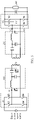
- FIG. 2 is a schematic diagram of a receive end of a wireless charging system of this application.
- the receive end of the wireless charging system provided in this invention includes a receive coil Cr, a rectifier, and a receive end controller 300.
- the receive coil receives an alternating magnetic field and outputs an alternating current.
- the rectifier rectifies the alternating current from the receive coil into a direct current.
- the rectifier is a full bridge rectifier or a half bridge rectifier.
- four switching transistors may all be controllable switching transistors, such as controllable switching transistors S1 to S4 shown in FIG. 2 , or may include two controllable switching transistors and two uncontrollable diodes.
- the receive end controller 300 adjusts, based on a target impedance sent by a transmit end controller, a reflection impedance reflected from the receive end to the transmit end, so that an inverter of the transmit end implements zero voltage switching; when the rectifier is a full bridge rectifier, the bridge arm voltage is a voltage between two bridge arm midpoints of the full bridge rectifier. As shown in FIG. 2 , the S1 and the S3 form a first bridge arm, the S2 and the S4 form a second bridge arm, a first bridge arm midpoint means a common end of the S1 and the S3, and a second bridge arm midpoint means a common end of the S2 and the S4. When the rectifier is a half bridge rectifier, the bridge arm voltage is a voltage between a single bridge arm midpoint of the half bridge rectifier and ground.
- the transmit end and the receive end are each provided with a wireless communications module, and the transmit end controller and the receive end controller 300 communicate with each other through their respective wireless communications modules.
- the transmit end controller sends the target impedance to the wireless communications module of the receive end through the wireless communications module of the transmit end, and then the wireless communications module of the receive end sends the received target impedance to the receive end controller 300.
- the inverter of the transmit end includes four controllable switching transistors Q1 to Q4. Because the inverter of the transmit end includes the controllable switching transistors, it is required to enable the controllable switching transistors to implement ZVS, thereby reducing power consumption generated by the controllable switching transistors in an action process.
- the reflection impedance reflected from the receive end to the transmit end is adjusted, to further adjust an equivalent output impedance of the inverter of the transmit end, so that a controllable switching transistor of the inverter is controlled to implement ZVS, and the receive end adjusts the reflection impedance based on the target impedance sent from the transmit end, that is, a reflection impedance required by the transmit end is used as the target impedance, so that the receive end adjusts a reflection impedance of the receive end so that the reflection impedance meets a requirement of the transmit end.
- the equivalent output impedance of the inverter exhibits a resistance inductivity
- the controllable switching transistor of the inverter may be enabled to implement ZVS.
- the reflection impedance of the receive end is mainly adjusted by adjusting a phase difference between a bridge arm voltage and an input current of the rectifier.
- FIG. 3 is a waveform diagram of the bridge arm voltage and the input current of the rectifier.
- U2 is the bridge arm voltage of the rectifier, and 12 is the input current of the rectifier.
- a phase of the bridge arm voltage U2 lags behind a phase of the input current 12, where an angle of the lag is ⁇ , that is, the phase difference between the bridge arm voltage and the input current of the rectifier is ⁇ .
- the phase difference ⁇ may be adjusted according to a need.
- an equivalent input impedance of the rectifier may be enabled to exhibit a resistance capacitivity.
- the receive end provided in in embodiments of this invention may further include a receive end LCC compensation network, where the receive end LCC compensation network is connected between the receive coil and the rectifier, and is configured to compensate the alternating current output by the receive coil and then send the compensated alternating current to the rectifier.
- the technical solution provided herein may include compensation networks applied to both the transmit end and the receive end being of an LCC structure.
- FIG. 4 is a schematic diagram of a compensation network that is of an LCC structure. It may be learned from the figure that, LCC includes one inductor L and two capacitors C.
- FIG. 5 is a schematic diagram of a transmit end and a receive end that are both LCC compensation networks. It may be learned from FIG. 5 that, the transmit end includes LCC and the receive end also includes LCC.
- FIG. 6 is an equivalent schematic diagram of a compensation network that is an LCC wireless charging system.
- An inverter of a transmit end is equivalent to an alternating voltage source, and a rectifier of a receive end is equivalent to a variable load Z2.
- compensation networks of the transmit end and the receive end are both LCC, and an equivalent circuit may be obtained as shown in FIG. 6 .
- a receive end controller adjusts an equivalent input impedance of a rectifier to further adjust a reflection impedance, and an operation principle thereof is described in detail below with reference to a flowchart.
- FIG. 7 is a flowchart of adjusting a reflection impedance by a receive end controller.
- the receive end controller receives a target impedance sent by a transmit end controller.
- the receive end controller obtains a corresponding target input impedance of a rectifier based on the target impedance.
- the receive end controller After obtaining the target input impedance of the rectifier, the receive end controller needs to first determine whether the target input impedance is within an adjustable impedance range of a receive end, and if the target input impedance is not within the adjustable impedance range of the receive end, waits for the transmit end controller to send a new target impedance. If the target input impedance is within the adjustable impedance range of the receive end, S704 is performed.
- the receive end controller obtains an equivalent input impedance of the rectifier.
- the receive end controller obtains the equivalent input impedance of the rectifier based on an input current and a bridge arm voltage of the rectifier, that is, the bridge arm voltage divided by the input current is the equivalent input impedance of the rectifier.
- That the equivalent input impedance of the rectifier exhibits a capacitivity greater than that of the target impedance is specifically: an imaginary part of the equivalent input impedance of the rectifier is a negative value, an imaginary part of the target impedance is a negative value, and an absolute value of the imaginary part of the equivalent input impedance of the rectifier is greater than an absolute value of the imaginary part of the target impedance.
- Im2 is an imaginary part, and represents a capacitive part or an inductive part.
- Im2 >0 it indicates that the imaginary part is positive and is an inductive impedance, and in this case, a phase of a current on the Im2 lags behind a phase of a voltage on the Im2 by 90 degrees.
- Im2 ⁇ When Im2 ⁇ 0, it indicates that the imaginary part is negative and is a capacitive impedance, and in this case, a phase of a current on the Im2 is ahead of a phase of a voltage on the Im2 by 90 degrees.
- a large capacitivity means that an absolute value of Im2 is relatively large.
- phase difference between the input current and the bridge arm voltage of the rectifier is adjusted so that a reflection impedance of the receive end is consistent with the target impedance.
- the receive end may adjust the capacitivity value of the equivalent input impedance of the rectifier by adjusting the phase difference between the input current and the bridge arm voltage of the rectifier. Because a capacitivity of the equivalent input impedance of the rectifier may be adjusted to adjust a value of the reflection impedance reflected from the receive end to a transmit end, so that the reflection impedance actually reflected from the receive end to the transmit end is consistent with a reflection impedance required by the transmit end, and therefore, it is possible to ensure that an inverter of the transmit end implements ZVS.
- the ZVS of the inverter is implemented by adjusting the reflection impedance of the receive end, that is, the rectifier is considered as a load with a variable impedance, and an impedance of the inverter itself does not need to be adjusted.
- the receive end controller is specifically configured to obtain the target input impedance of the rectifier based on the target impedance, a modulus value of an impedance of each branch in the receive end LCC compensation network, and a mutual inductance between a transmit coil and a receive coil.
- FIG. 8a is an equivalent circuit diagram of a receive end of this application
- FIG. 8a is an equivalent circuit corresponding to a receive end LCC compensation network.
- a target impedance Zr includes a real part Rzr and an imaginary part Xzr, as shown in the following formula.
- a target input impedance Zrec of a rectifier may be obtained by using the following formula, where X2 is a modulus value of an impedance of each branch in the receive end LCC compensation network and the modulus value means an absolute value of the impedance.
- M is a mutual inductance between a transmit coil and a receive coil.
- FIG. 8b is a schematic diagram of a transmit end in a wireless charging system according to this application.
- the transmit end of the wireless charging system includes a transmit coil Ct, an inverter HI, and a transmit end controller 300.
- the inverter HI is configured to invert a direct current output by a direct current power source into an alternating current. It may be understood that when the field of application of the wireless charging system is an electric vehicle, the transmit end is provided on ground, the receive end is provided on the electric vehicle, and the transmit end and the receive end wirelessly communicate with each other. In addition, charging is performed wirelessly, and specifically, energy is transferred by using an alternating magnetic field.
- the transmit coil Ct is configured to transmit the alternating current in a form of an alternating magnetic field.
- the transmit end controller 300 is configured to: obtain a target impedance based on an input voltage of the inverter HI, a phase difference between two bridge arms of the inverter HI, and a power that the wireless charging system needs to output, and send the target impedance to the receive end controller 400, so that the receive end controller 400 controls a reflection impedance of the receive end to be consistent with the target impedance.
- Two bridge arms of the HI are bridge arms respectively formed by Q1 and Q3, and bridge arms respectively formed by Q2 and Q4.
- An input voltage of the HI means an output voltage of a direct current power source, and a method for obtaining the target impedance is described below with reference to an equivalent circuit diagram of the transmit end.
- FIG. 9 is an equivalent circuit diagram of a transmit end of this application Uinv represents a direct current power source and Ubus represents a voltage of Uinv.
- a transmit end controller 300 obtains a target impedance based on Ubus and a phase difference between two bridge arms of the HI, and a power Po that a receive end needs to output, which may be specifically obtained by using the following formula.
- R Zr P o ⁇ X 2 2 2 ⁇ ⁇ U bus ⁇ sin ⁇ 2 2
- X Zr P o ⁇ X 2 ⁇ tan ⁇ ⁇ ⁇ 2 2 2 ⁇ ⁇ U bus ⁇ sin ⁇ 2 2
- Po is a power that a wireless charging system needs to output, for example, when applied to the field of electric vehicles, a value of Po is determined by a battery of an electric vehicle.
- the transmit end controller 300 obtains a target impedance of a reflection impedance according to Formula (1) and Formula (2), that is, a value of a reflection impedance that needs to be reflected by the receive end.
- a target impedance of a reflection impedance according to Formula (1) and Formula (2) that is, a value of a reflection impedance that needs to be reflected by the receive end.
- the target impedance cannot be reached by adjusting the reflection impedance at one time.
- the transmit end controller 300 is further configured to: obtain the reflection impedance of the receive end based on an output voltage and an output current of the transmit end, compare the reflection impedance of the receive end with the target impedance, and if the reflection impedance of the receive end is consistent with the target impedance, send, to the receive end controller 400, a message to end adjustment of a phase difference between the input current and the bridge arm voltage of the rectifier.
- An equivalent circuit diagram shown in FIG. 9 includes three impedance branches: a first branch including jX, a second branch including -jX, and a third branch including jX and a reflection impedance Z.
- the three branches of a transmit end LCC compensation network include equal modulus values of impedances, that is, an impedance of each branch is X.
- the transmit end controller 300 obtains the value of the reflection impedance based on a voltage and a current of the third branch.
- FIG. 10 is a waveform diagram of a voltage and a current of a third branch corresponding to FIG. 9 .
- the voltage of the third branch is ahead of the current of the third branch by a phase ⁇ . That is, a phase difference between the voltage and the current of the third branch is ⁇ .
- An imaginary part of the reflection impedance Z (a voltage peak of the transmit coil/a current peak of the transmit coil) ⁇ sin ⁇ - X.
- the real part and the imaginary part of the target impedance Zr are calculated in Formula (1) and Formula (2), while the real part and the imaginary part of Z are a real part and an imaginary part of the actual reflection impedance.
- the transmit end controller 300 may determine, based on the real part and the imaginary part of the actual reflection impedance, whether the receive end needs to continue adjusting a phase difference between a bridge arm voltage and an input current of the rectifier. When the real part and the imaginary part of the actual reflection impedance are respectively consistent with the real part and the imaginary part of the target impedance, it is not necessary to continue adjusting the phase difference between the bridge arm voltage and the input current of the rectifier.
- Example of a wireless charging system Based on the receive end and the transmit end of the wireless charging system provided in the foregoing parts of the present description, it is as well provided a wireless charging system, and the wireless charging system includes the transmit end and the receive end described earlier herein.
- the wireless charging system further includes a power battery string.
- the receive end charges the power battery string.
- the receive end When the wireless charging system is applied to the field of electric vehicles, the receive end is located on an electric vehicle, and the receive end charges a power battery string of the electric vehicle, that is, the power battery string supplies energy to the electric vehicle is supplying power by a motor on the electric vehicle, and the motor supplies a driving force to the electric vehicle.
- the transmit end included in the wireless charging system may implement ZVS of the inverter, thereby reducing a loss generated by a controllable switching transistor of the inverter in an operation process, and further improving electric energy transmission efficiency of a transmit coil and a receive coil.
- FIG. 11 is a waveform diagram corresponding to a difference of 2.75 ⁇ s between a bridge arm voltage U1 of an inverter and a bridge arm voltage U2 of a rectifier of this application
- FIG. 12 is a waveform diagram corresponding to a difference of 1.75 ⁇ s between a bridge arm voltage U1 of an inverter and a bridge arm voltage U2 of a rectifier of this application It may be understood that a phase of U2 is ahead of a phase of U1.
- a relatively large equivalent impedance capacitivity on a receive side for example, a positive current of I2 in a case of 1.75 ⁇ s is greater than a positive current of 12 in a case of 2.75 ⁇ s
- a relatively large equivalent impedance inductivity of the transmit end for example, a negative current of I1 in a case of 2.75 ⁇ s is less than a negative current of I1 in a case of 1.75 ⁇ s
- turn-on losses of the inverter and the rectifier are increased. Therefore, an angle by which the receive side is ahead of may be appropriately increased to decrease a reactive current, thereby achieving a smaller turn-on loss. Because the turn-on loss is directly proportional to the square of a current, the reactive current decreases, and a current on the controllable switching transistor decreases.
- At least one of a, b, or c may represent a, b, c, "a and b", “a and c", “b and c", or "a, b, and c", where a, b, c may be a single one or a plurality of.
Landscapes
- Engineering & Computer Science (AREA)
- Power Engineering (AREA)
- Computer Networks & Wireless Communication (AREA)
- Transportation (AREA)
- Mechanical Engineering (AREA)
- Charge And Discharge Circuits For Batteries Or The Like (AREA)
Description
- The present invention relates to the field of power electronics technologies, and in particular, to a receive end and a transmit end of a wireless charging system, and a wireless charging system
- With aggravation of energy shortage and environmental pollution problems of modern society, as a new energy vehicle, an electric vehicle attracts wide attention once launched. However, most of existing electric vehicles are limited by a battery capacity, and can run for a relatively short distance. In addition, a long battery charging time and shortage of corresponding charging station resources of electric vehicles become biggest bottlenecks that impede application and popularization of electric vehicles.
- Methods for charging a battery of an electric vehicle usually include contact charging and wireless charging. The contact charging means electricity conduction through metallic contact between a plug and a socket, and the wireless charging means transferring electric energy by using a coupled alternating magnetic field as a medium Compared with the contact charging, the wireless charging has many advantages and has become a main manner of charging the electric vehicle in the future.
- An operation principle of a wireless charging system is described below with reference to an accompanying drawing.
FIG. 1 is a schematic diagram of a wireless charging system - The wireless charging system includes a transmit end and a receive end. The transmit end includes an inverter HI, a transmit
end compensation network 100, a transmitend controller 400, and a transmit coil Ct. The receive end includes a rectifier H2, a receiveend compensation network 200, and a receiveend controller 300. - Because the HI is connected to a direct current power source, the HI is configured to invert a direct current into an alternating current. The transmit
end compensation network 100 compensates an alternating current output by the HI and then outputs the compensated alternating current to the transmit coil Ct, and the transmit coil Ct is configured to transmit the alternating current in a form of an alternating magnetic field. - A receive coil Cr of the receive end is configured to receive an alternating magnetic field and output an alternating current, the receive
end compensation network 200 is configured to compensate the alternating current and then output the compensated alternating current to the rectifier H2, and the H2 is configured to rectify the alternating current into a direct current and supply the direct current to a load. - The HI includes four controllable switching transistors Q1 to Q4 and the H2 includes four controllable switching transistors S1 to S4.
- Because the controllable switching transistor generates a loss in a switching process, it is desirable that the controllable switching transistor generates a loss as less as possible in the switching process, to improve operation efficiency of the wireless charging system.
-
CN 108656994 A discloses a transmitting end, which is configured to adjust the reflected impedance reflected from the receiving end to the transmitting end according to the target impedance sent by the transmitting end controller, so that the inverter at the transmitting end implements zero voltage switching. -
US 2017/025897 A1 discloses a method for adjusting the output power of the rectifier at the receiving end, without reflecting the output power to the primary side. - As used herein, the term capacitivity corresponds to capacitive impedance.
- To resolve the foregoing technical problems in the prior art, the present invention provides a receive end and a transmit end of a wireless charging system, and a wireless charging system, which can ensure that an inverter of the transmit end implements zero voltage switching, and reduce a loss generated by a controllable switching transistor, thereby improving operation efficiency of the wireless charging system.
- According to a first aspect, an embodiment of this application provides a receive end of a wireless charging system, including a receive coil, a rectifier, and a receive end controller, where the receive coil receives an alternating magnetic field and outputs an alternating current; the rectifier rectifies the alternating current from the receive coil into a direct current; the receive end controller adjusts, based on a target impedance sent by a transmit end controller, a reflection impedance reflected from the receive end to a transmit end, so that an inverter of the transmit end implements zero voltage switching; and the rectifier is either a full bridge rectifier or a half bridge rectifier, when the rectifier is a full bridge rectifier, a bridge arm voltage is a voltage between two bridge arm midpoints of a full bridge rectifier, and when the rectifier is a half bridge rectifier, a bridge arm voltage is a voltage between a single bridge arm midpoint of the half bridge rectifier and ground.
- The receive end adjusts the reflection impedance reflected from the receive end to the transmit end, to further adjust an equivalent output impedance of the inverter of the transmit end, so that a controllable switching transistor of the inverter implements zero voltage switching, and the receive end adjusts the reflection impedance based on the target impedance sent from the transmit end, that is, a reflection impedance required by the transmit end is used as the target impedance, so that the receive end adjusts an actual reflection impedance of the receive end based on the target impedance to meet a requirement of the transmit end. When the equivalent output impedance of the inverter exhibits a resistance inductivity, the controllable switching transistor of the inverter may be enabled to implement zero voltage switching.
- Specifically, in any of the embodiments directed to a receive end in the present invention, the receive end controller is further configured to: obtain a corresponding target input impedance of the rectifier based on the target impedance; and obtain an equivalent input impedance of the rectifier, compare the target input impedance of the rectifier with the equivalent input impedance, and adjust a phase difference between an input current and a bridge arm voltage of the rectifier based on a comparison result so that the reflection impedance is consistent with the target impedance.
- The phase difference between the input current and the bridge arm voltage of the rectifier is adjusted so that the reflection impedance of the receive end is consistent with the target impedance.
- The equivalent input impedance of the rectifier may be obtained based on the input current and the bridge arm voltage of the rectifier, that is, the bridge arm voltage divided by the input current is the equivalent input impedance.
- Preferably, the receive end controller is specifically configured to: compare the equivalent input impedance of the rectifier with the target input impedance, decrease the phase difference between the input current and the bridge arm voltage of the rectifier when the equivalent input impedance of the rectifier exhibits a capacitivity greater than that of the target input impedance, and increase the phase difference between the input current and the bridge arm voltage of the rectifier when the equivalent input impedance of the rectifier exhibits a capacitivity less than or equal to that of the target input impedance.
- Preferably, that the equivalent input impedance of the rectifier exhibits a capacitivity greater than that of the target impedance is specifically: an imaginary part of the equivalent input impedance of the rectifier is a negative value, an imaginary part of the target impedance is a negative value, and an absolute value of the imaginary part of the equivalent input impedance of the rectifier is greater than an absolute value of the imaginary part of the target impedance. Preferably, the receive end further includes a receive end LCC compensation network, where the receive end LCC compensation network is connected between the receive coil and the rectifier, and is configured to compensate the alternating current output by the receive coil and then send the compensated alternating current to the rectifier.
- The LCC compensation network includes three branches, one inductive branch and two capacitive branches, and the three branches exhibit equal impedance modulus values. Usually, architectures of compensation networks of the receive end and the transmit end are the same, that is, both LCC compensation networks.
- Preferably, the receive end controller is specifically configured to obtain the target input impedance of the rectifier based on the target impedance, a modulus value of an impedance of each branch in the receive end LCC compensation network, and a mutual inductance between a transmit coil and the receive coil.
- According to a second aspect, an embodiment of this application further provides a transmit end of a wireless charging system, including a transmit coil, an inverter, and a transmit end controller, where the inverter inverts a direct current output by a direct current power source into an alternating current; the transmit coil transmits the alternating current in a form of an alternating magnetic field; and the transmit end controller obtains a target impedance based on an input voltage of the inverter, a phase difference between two bridge arms of the inverter, and a power that the wireless charging system needs to output, and sends the target impedance to a receive end controller, so that the receive end controller controls a reflection impedance of a receive end to be consistent with the target impedance.
- The transmit end may obtain a reflection impedance required by the transmit end, and send the reflection impedance as the target impedance to the receive end controller, and when the reflection impedance reflected by the receive end is used to enable an equivalent output impedance of the inverter of the transmit end to exhibit a resistance inductivity, a controllable switching transistor of the inverter may be enabled to implement zero voltage switching.
- Specifically, in any of the embodiments directed to a transmit end in the present invention, the transmit end controller is further configured to: obtain the reflection impedance of the receive end based on an output voltage and an output current of the transmit end, compare the reflection impedance of the receive end with the target impedance, and if the reflection impedance of the receive end is consistent with the target impedance, send, to the receive end controller, a message to end adjustment of a phase difference between an input current and a bridge arm voltage of a rectifier.
- According to a third aspect, an embodiment of this application further provides a wireless charging system, including a power battery string, the receive end described above, and the transmit end described above, where the receive end charges the power battery string.
- Compared with the prior art, the present invention has at least the following advantages:
The receive end adjusts the reflection impedance reflected from the receive end to the transmit end, to further adjust the equivalent output impedance of the inverter of the transmit end, so that the controllable switching transistor of the inverter implements zero voltage switching (ZVS), and the receive end adjusts the reflection impedance based on the target impedance sent from the transmit end, that is, a reflection impedance required by the transmit end is used as the target impedance, so that the receive end adjusts the actual reflection impedance of the receive end based on the target impedance to meet the requirement of the transmit end. When the equivalent output impedance of the inverter exhibits a resistance inductivity, the controllable switching transistor of the inverter may be enabled to implement ZVS. When the controllable switching transistor of the inverter implements ZVS, power consumption generated in an operation process of the controllable switching transistor may be reduced, thereby improving operation efficiency of the wireless charging system. - To describe the technical solutions of this application more clearly, the following briefly describes the accompanying drawings required for describing the the teachings of the present disclosure or the prior art. Apparently, the accompanying drawings in the following description show some features of this application.
-
FIG. 1 is a schematic diagram of a wireless charging system; -
FIG. 2 is a schematic diagram of a receive end of a wireless charging system; -
FIG. 3 is a waveform diagram of a bridge arm voltage and an input current of a rectifier; -
FIG. 4 is a schematic diagram of a compensation network that is of an LCC structure; -
FIG. 5 is a schematic diagram of a transmit end and a receive end that are both LCC compensatior networks; -
FIG. 6 is an equivalent schematic diagram of a compensation network that is an LCC wireless charging system; -
FIG. 7 is a flowchart of adjusting a reflection impedance by a receive end controller; -
FIG. 8a is an equivalent circuit diagram of a receive end; -
FIG. 8b is a schematic diagram of a transmit end in a wireless charging system; -
FIG. 9 is an equivalent circuit diagram of a transmit end; -
FIG. 10 is a waveform diagram of a voltage and a current of a third branch corresponding toFIG. 9 ; -
FIG. 11 is a waveform diagram corresponding to a difference of 2.75 µs between a bridge arm voltage U1 of an inverter and a bridge arm voltage U2 of a rectifier; and -
FIG. 12 is a waveform diagram corresponding to a difference of 1.75 µs between a bridge arm voltage U1 of an inverter and a bridge arm voltage U2 of a rectifier. - To enable a person skilled in the art to better understand the technical solutions provided in this application, an application scenario is first described below. A receive end provided in this application is applied to a wireless charging system. Specifically, referring to
FIG. 1, FIG. 1 is a schematic diagram of a wireless charging system. - The wireless charging system may wirelessly charge an electric terminal, that is, a transmit end and a receive end are not connected through a wire, but wirelessly transfer electromagnetic energy through alternating magnetic field interaction.
- In actual application, the transmit end of the wireless charging system usually includes an inverter HI, a transmit
end compensation circuit 100, and a transmit coil Ct. The HI inFIG. 1 includes four controllable switching transistors that are Q1 to Q4, respectively. A function of the inverter HI is to invert a direct current output by a direct current power source into an alternating current; a function of the transmitend compensation circuit 100 is to compensate the alternating current and then output the compensated alternating current to the transmit coil Ct; a function of the transmit coil Ct is to transmit the alternating current in a form of an alternating magnetic field so that a receive coil Cr wirelessly receives the alternating magnetic field. - The receive end includes the receive coil Cr, a receive
end compensation network 200, and a rectifier H2. The receive coil Cr is configured to receive an alternating magnetic field from the transmit coil Ct and output an alternating current. The receiveend compensation network 200 is configured to compensate the alternating current and output the compensated alternating current to the rectifier H2. The rectifier H2 includes controllable switching transistors S1 to S4. A receiveend controller 300 communicates wirelessly with a transmitend controller 400. - The rectifier H2 is either a full bridge rectifier or a half bridge rectifier. When the rectifier is a full bridge rectifier, the four switching transistors may all be controllable switching transistors, or may include two controllable switching transistors and two uncontrollable diodes.
- The transmit
end controller 400 communicates wirelessly with the receiveend controller 300. Manners of wireless communication may include but are not limited to any one or any combination of the following manners: Bluetooth, Wireless Fidelity (WiFi), Zigbee, a radio frequency identification (RFID) technology, long range (Lora) wireless technology, and a Near Field Communication (NFC) technology. - For the inverter of the transmit end of the wireless charging system, to ensure that a controllable switching transistor of the inverter implements a zero voltage switching (ZVS) effect, an equivalent output impedance of the inverter is required to exhibit a specific resistance inductivity when the inverter implements ZVS, that is, the inverter can output a specific ZVS reactive power, and a value of the inductivity needs to be suitable. The ZVS means that a value of a voltage across both ends of a controllable switching transistor is ideally 0 when the controllable switching transistor is turned off and turned on. Certainly, in actual application, the voltage across both ends of the controllable switching transistor may be a relatively small voltage, and a smaller voltage leads to lower power consumption. A lack of an inductivity may cause the inverter to lose the ZVS effect, cause an increase in switching losses, or even cause damage to the inverter. If the inductivity is high, the reactive power output by the inverter is relatively large, which causes a turn-on loss of the inverter to increase and efficiency to decrease. Therefore, the inverter of the transmit end is enabled to implement ZVS, thereby achieving efficiency optimization of the wireless charging system.
- According to the technical solutions provided in the embodiments of this application, a reflection impedance reflected from the receive end to the transmit end is adjusted, so that a controllable switching transistor of the inverter of the transmit end implements ZVS.
- To make a person skilled in the art understand the technical solutions in the present invention better, the following clearly describes the technical solutions in the embodiments of the present invention with reference to the accompanying drawings in the embodiments of the present invention.
- First example of a receive end:
FIG. 2 is a schematic diagram of a receive end of a wireless charging system of this application. - The receive end of the wireless charging system provided in this invention includes a receive coil Cr, a rectifier, and a receive
end controller 300. - The receive coil receives an alternating magnetic field and outputs an alternating current.
- The rectifier rectifies the alternating current from the receive coil into a direct current.
- The rectifier is a full bridge rectifier or a half bridge rectifier. When the rectifier is a full bridge rectifier, four switching transistors may all be controllable switching transistors, such as controllable switching transistors S1 to S4 shown in
FIG. 2 , or may include two controllable switching transistors and two uncontrollable diodes. - The receive
end controller 300 adjusts, based on a target impedance sent by a transmit end controller, a reflection impedance reflected from the receive end to the transmit end, so that an inverter of the transmit end implements zero voltage switching; when the rectifier is a full bridge rectifier, the bridge arm voltage is a voltage between two bridge arm midpoints of the full bridge rectifier. As shown inFIG. 2 , the S1 and the S3 form a first bridge arm, the S2 and the S4 form a second bridge arm, a first bridge arm midpoint means a common end of the S1 and the S3, and a second bridge arm midpoint means a common end of the S2 and the S4. When the rectifier is a half bridge rectifier, the bridge arm voltage is a voltage between a single bridge arm midpoint of the half bridge rectifier and ground. - It may be understood that the transmit end and the receive end are each provided with a wireless communications module, and the transmit end controller and the receive
end controller 300 communicate with each other through their respective wireless communications modules. For example, the transmit end controller sends the target impedance to the wireless communications module of the receive end through the wireless communications module of the transmit end, and then the wireless communications module of the receive end sends the received target impedance to the receiveend controller 300. - As shown in
FIG. 2 , the inverter of the transmit end includes four controllable switching transistors Q1 to Q4. Because the inverter of the transmit end includes the controllable switching transistors, it is required to enable the controllable switching transistors to implement ZVS, thereby reducing power consumption generated by the controllable switching transistors in an action process. - In the present invention, the reflection impedance reflected from the receive end to the transmit end is adjusted, to further adjust an equivalent output impedance of the inverter of the transmit end, so that a controllable switching transistor of the inverter is controlled to implement ZVS, and the receive end adjusts the reflection impedance based on the target impedance sent from the transmit end, that is, a reflection impedance required by the transmit end is used as the target impedance, so that the receive end adjusts a reflection impedance of the receive end so that the reflection impedance meets a requirement of the transmit end. When the equivalent output impedance of the inverter exhibits a resistance inductivity, the controllable switching transistor of the inverter may be enabled to implement ZVS.
- The reflection impedance of the receive end is mainly adjusted by adjusting a phase difference between a bridge arm voltage and an input current of the rectifier. Specifically, referring to
FIG. 3, FIG. 3 is a waveform diagram of the bridge arm voltage and the input current of the rectifier. - In
FIG. 3 , U2 is the bridge arm voltage of the rectifier, and 12 is the input current of the rectifier. - It may be learned from the figure that, a phase of the bridge arm voltage U2 lags behind a phase of the input current 12, where an angle of the lag is θ, that is, the phase difference between the bridge arm voltage and the input current of the rectifier is θ. The phase difference θ may be adjusted according to a need. When the phase of U2 lags behind that of 12, an equivalent input impedance of the rectifier may be enabled to exhibit a resistance capacitivity.
- The receive end provided in in embodiments of this invention may further include a receive end LCC compensation network, where the receive end LCC compensation network is connected between the receive coil and the rectifier, and is configured to compensate the alternating current output by the receive coil and then send the compensated alternating current to the rectifier.
- It should be noted that the technical solution provided herein may include compensation networks applied to both the transmit end and the receive end being of an LCC structure.
- It may be understood that the compensation networks of the transmit end and the receive end may be of an LC structure, or may be of a single C structure, or the like in addition to the LCC structure, and details are not described herein. Specifically, referring to
FIG. 4, FIG. 4 is a schematic diagram of a compensation network that is of an LCC structure. It may be learned from the figure that, LCC includes one inductor L and two capacitors C. - For a wireless charging system in which the compensation networks of the transmit end and the receive end are both of an LCC structure, specifically, referring to
FIG. 5, FIG. 5 is a schematic diagram of a transmit end and a receive end that are both LCC compensation networks. It may be learned fromFIG. 5 that, the transmit end includes LCC and the receive end also includes LCC. - Second example of a receive end:
FIG. 6 is an equivalent schematic diagram of a compensation network that is an LCC wireless charging system. - An inverter of a transmit end is equivalent to an alternating voltage source, and a rectifier of a receive end is equivalent to a variable load Z2. For example, compensation networks of the transmit end and the receive end are both LCC, and an equivalent circuit may be obtained as shown in
FIG. 6 . - A receive end controller adjusts an equivalent input impedance of a rectifier to further adjust a reflection impedance, and an operation principle thereof is described in detail below with reference to a flowchart.
-
FIG. 7 is a flowchart of adjusting a reflection impedance by a receive end controller. - S701. The receive end controller receives a target impedance sent by a transmit end controller.
- S702. The receive end controller obtains a corresponding target input impedance of a rectifier based on the target impedance.
- After obtaining the target input impedance of the rectifier, the receive end controller needs to first determine whether the target input impedance is within an adjustable impedance range of a receive end, and if the target input impedance is not within the adjustable impedance range of the receive end, waits for the transmit end controller to send a new target impedance. If the target input impedance is within the adjustable impedance range of the receive end, S704 is performed.
- S703. The receive end controller obtains an equivalent input impedance of the rectifier.
- Specifically, the receive end controller obtains the equivalent input impedance of the rectifier based on an input current and a bridge arm voltage of the rectifier, that is, the bridge arm voltage divided by the input current is the equivalent input impedance of the rectifier.
- S704. Compare a capacitivity value of the target input impedance and that of the equivalent input impedance of the rectifier.
- S705. Decrease a phase difference between the input current and the bridge arm voltage of the rectifier when the equivalent input impedance of the rectifier exhibits a capacitivity greater than that of the target input impedance, and increase the phase difference between the input current and the bridge arm voltage of the rectifier when the equivalent input impedance of the rectifier exhibits a capacitivity less than or equal to that of the target input impedance.
- That the equivalent input impedance of the rectifier exhibits a capacitivity greater than that of the target impedance is specifically:
an imaginary part of the equivalent input impedance of the rectifier is a negative value, an imaginary part of the target impedance is a negative value, and an absolute value of the imaginary part of the equivalent input impedance of the rectifier is greater than an absolute value of the imaginary part of the target impedance. - For example, Z2 is used to represent the equivalent input impedance of the rectifier, Z2 = R2 + jIm2, where R2 represents a real part, represents a resistive part, and a current flowing through the R2 is in phase with a voltage across both ends of the R2. Im2 is an imaginary part, and represents a capacitive part or an inductive part. When Im2 > 0, it indicates that the imaginary part is positive and is an inductive impedance, and in this case, a phase of a current on the Im2 lags behind a phase of a voltage on the Im2 by 90 degrees. When Im2 < 0, it indicates that the imaginary part is negative and is a capacitive impedance, and in this case, a phase of a current on the Im2 is ahead of a phase of a voltage on the Im2 by 90 degrees. A large capacitivity means that an absolute value of Im2 is relatively large.
- The phase difference between the input current and the bridge arm voltage of the rectifier is adjusted so that a reflection impedance of the receive end is consistent with the target impedance.
- The receive end may adjust the capacitivity value of the equivalent input impedance of the rectifier by adjusting the phase difference between the input current and the bridge arm voltage of the rectifier. Because a capacitivity of the equivalent input impedance of the rectifier may be adjusted to adjust a value of the reflection impedance reflected from the receive end to a transmit end, so that the reflection impedance actually reflected from the receive end to the transmit end is consistent with a reflection impedance required by the transmit end, and therefore, it is possible to ensure that an inverter of the transmit end implements ZVS. The ZVS of the inverter is implemented by adjusting the reflection impedance of the receive end, that is, the rectifier is considered as a load with a variable impedance, and an impedance of the inverter itself does not need to be adjusted.
- The receive end controller is specifically configured to obtain the target input impedance of the rectifier based on the target impedance, a modulus value of an impedance of each branch in the receive end LCC compensation network, and a mutual inductance between a transmit coil and a receive coil.
- A process in which the receive end controller obtains the target input impedance is described below with reference to the accompanying drawings.
FIG. 8a is an equivalent circuit diagram of a receive end of this applicationFIG. 8a is an equivalent circuit corresponding to a receive end LCC compensation network. A target impedance Zr includes a real part Rzr and an imaginary part Xzr, as shown in the following formula. A target input impedance Zrec of a rectifier may be obtained by using the following formula, where X2 is a modulus value of an impedance of each branch in the receive end LCC compensation network and the modulus value means an absolute value of the impedance. M is a mutual inductance between a transmit coil and a receive coil.

- First example of a transmit end:
FIG. 8b is a schematic diagram of a transmit end in a wireless charging system according to this application. - The transmit end of the wireless charging system provided includes a transmit coil Ct, an inverter HI, and a transmit
end controller 300. - The inverter HI is configured to invert a direct current output by a direct current power source into an alternating current. It may be understood that when the field of application of the wireless charging system is an electric vehicle, the transmit end is provided on ground, the receive end is provided on the electric vehicle, and the transmit end and the receive end wirelessly communicate with each other. In addition, charging is performed wirelessly, and specifically, energy is transferred by using an alternating magnetic field.
- The transmit coil Ct is configured to transmit the alternating current in a form of an alternating magnetic field.
- The transmit
end controller 300 is configured to: obtain a target impedance based on an input voltage of the inverter HI, a phase difference between two bridge arms of the inverter HI, and a power that the wireless charging system needs to output, and send the target impedance to the receiveend controller 400, so that the receiveend controller 400 controls a reflection impedance of the receive end to be consistent with the target impedance. - Two bridge arms of the HI are bridge arms respectively formed by Q1 and Q3, and bridge arms respectively formed by Q2 and Q4.
- An input voltage of the HI means an output voltage of a direct current power source, and a method for obtaining the target impedance is described below with reference to an equivalent circuit diagram of the transmit end.
-
FIG. 9 is an equivalent circuit diagram of a transmit end of this application Uinv represents a direct current power source and Ubus represents a voltage of Uinv. - A transmit
end controller 300 obtains a target impedance based on Ubus and a phase difference between two bridge arms of the HI, and a power Po that a receive end needs to output, which may be specifically obtained by using the following formula. - A real part Rzr of the target impedance is Formula (1):

- An imaginary part Xzr of the target impedance is Formula (2):

- Po is a power that a wireless charging system needs to output, for example, when applied to the field of electric vehicles, a value of Po is determined by a battery of an electric vehicle.
- It may be understood that the transmit
end controller 300 obtains a target impedance of a reflection impedance according to Formula (1) and Formula (2), that is, a value of a reflection impedance that needs to be reflected by the receive end. However, in actual operation, usually, the target impedance cannot be reached by adjusting the reflection impedance at one time. Therefore, the transmitend controller 300 is further configured to: obtain the reflection impedance of the receive end based on an output voltage and an output current of the transmit end, compare the reflection impedance of the receive end with the target impedance, and if the reflection impedance of the receive end is consistent with the target impedance, send, to the receiveend controller 400, a message to end adjustment of a phase difference between the input current and the bridge arm voltage of the rectifier. - A manner in which the transmit
end controller 300 obtains an actual reflection impedance is described below with reference toFIG. 9 . - An equivalent circuit diagram shown in
FIG. 9 includes three impedance branches: a first branch including jX, a second branch including -jX, and a third branch including jX and a reflection impedance Z. The three branches of a transmit end LCC compensation network include equal modulus values of impedances, that is, an impedance of each branch is X. - The transmit
end controller 300 obtains the value of the reflection impedance based on a voltage and a current of the third branch. -
FIG. 10 is a waveform diagram of a voltage and a current of a third branch corresponding toFIG. 9 . - The voltage of the third branch is ahead of the current of the third branch by a phase α. That is, a phase difference between the voltage and the current of the third branch is α.
- Then, a real part of a reflection impedance Z = (a voltage peak of a transmit coil/a current peak of the transmit coil) ∗ cos α.
- An imaginary part of the reflection impedance Z = (a voltage peak of the transmit coil/a current peak of the transmit coil) ∗ sin α - X.
- It may be understood that the real part and the imaginary part of the target impedance Zr are calculated in Formula (1) and Formula (2), while the real part and the imaginary part of Z are a real part and an imaginary part of the actual reflection impedance. The transmit
end controller 300 may determine, based on the real part and the imaginary part of the actual reflection impedance, whether the receive end needs to continue adjusting a phase difference between a bridge arm voltage and an input current of the rectifier. When the real part and the imaginary part of the actual reflection impedance are respectively consistent with the real part and the imaginary part of the target impedance, it is not necessary to continue adjusting the phase difference between the bridge arm voltage and the input current of the rectifier. - Example of a wireless charging system:
Based on the receive end and the transmit end of the wireless charging system provided in the foregoing parts of the present description, it is as well provided a wireless charging system, and the wireless charging system includes the transmit end and the receive end described earlier herein. - The wireless charging system further includes a power battery string.
- The receive end charges the power battery string.
- When the wireless charging system is applied to the field of electric vehicles, the receive end is located on an electric vehicle, and the receive end charges a power battery string of the electric vehicle, that is, the power battery string supplies energy to the electric vehicle is supplying power by a motor on the electric vehicle, and the motor supplies a driving force to the electric vehicle.
- Because the transmit end included in the wireless charging system may implement ZVS of the inverter, thereby reducing a loss generated by a controllable switching transistor of the inverter in an operation process, and further improving electric energy transmission efficiency of a transmit coil and a receive coil.
- To intuitively understand the beneficial effects of the technical solutions provided herein, the following is described in detail with reference to an experimental simulation waveform diagram
FIG. 11 is a waveform diagram corresponding to a difference of 2.75 µs between a bridge arm voltage U1 of an inverter and a bridge arm voltage U2 of a rectifier of this applicationFIG. 12 is a waveform diagram corresponding to a difference of 1.75 µs between a bridge arm voltage U1 of an inverter and a bridge arm voltage U2 of a rectifier of this application It may be understood that a phase of U2 is ahead of a phase of U1. - By comparing
FIG. 11 and FIG. 12 , it may be learned that because an angle by which the bridge arm voltage of the rectifier is ahead of is decreased, that is, from 2.75 µs to 1.75 µs. It may be learned that a negative current of an I1 current line marked by a circle is increased, and that a larger negative current makes it easier to implement ZVS. Therefore, it is more advantageous for a controllable switching transistor of an inverter of a transmit end to implement ZVS. - It may be learned that a relatively large equivalent impedance capacitivity on a receive side (for example, a positive current of I2 in a case of 1.75 µs is greater than a positive current of 12 in a case of 2.75 µs) leads to a relatively large equivalent impedance inductivity of the transmit end (for example, a negative current of I1 in a case of 2.75 µs is less than a negative current of I1 in a case of 1.75 µs), and in this case, turn-on losses of the inverter and the rectifier are increased. Therefore, an angle by which the receive side is ahead of may be appropriately increased to decrease a reactive current, thereby achieving a smaller turn-on loss. Because the turn-on loss is directly proportional to the square of a current, the reactive current decreases, and a current on the controllable switching transistor decreases.
- It should be understood that "at least one" in this application means one or more, and "a plurality of' means two or more. "and/or" is used to describe an association relationship between associated objects and represents that three relationships may exist. For example, "A and/or B" may represent the following three cases: Only A exists, only B exists, and both A and B exist, where A and B each may be singular or plural. The character "/" generally indicates an "or" relationship between the associated objects. "at least one of the following" or similar expressions thereof mean any combination of these, including a single one or any combination of plural items. For example, at least one of a, b, or c may represent a, b, c, "a and b", "a and c", "b and c", or "a, b, and c", where a, b, c may be a single one or a plurality of.
- The present invention is defined by the appended claims.
Claims (8)
- A receive end of a wireless charging system, comprising a receive coil (Cr), a rectifier (H2), and a receive end controller, wherein the receive coil is configured to receive an alternating magnetic field and output an alternating current:the rectifier is configured to rectify the alternating current from the receive coil into a direct current; andthe receive end controller is configured to adjust, based on a target impedance sent by a transmit end controller, a reflection impedance reflected from the receive end to the transmit end, so that an inverter of the transmit end implements zero voltage switching; and a bridge arm voltage is a voltage between two bridge arm midpoints of a full bridge rectifier or a voltage between a single bridge arm midpoint of a half bridge rectifier and ground;wherein the rectifier is a full bridge rectifier comprising at least two controllable switching transistors or a half bridge rectifier comprising two controllable switching transistors;the receive end controller is specifically configured to obtain a corresponding target input impedance of the rectifier based on the target impedance; andobtain an equivalent input impedance of the rectifier, compare the corresponding target input impedance of the rectifier with the equivalent input impedance, and adjust a phase difference between an input current and a bridge arm voltage of the rectifier based on a comparison result so that the reflection impedance is consistent with the target impedance.
- The receive end according to claim 1, wherein the receive end controller is specifically configured to:
compare the equivalent input impedance of the rectifier with the corresponding target input impedance of the rectifier, decrease the phase difference between the input current and the bridge arm voltage of the rectifier when the equivalent input impedance of the rectifier exhibits a capacitive impedance greater than that of the corresponding target input impedance of the rectifier, and increase the phase difference between the input current and the bridge arm voltage of the rectifier when the equivalent input impedance of the rectifier exhibits a capacitive impedance less than or equal to that of the corresponding target input impedance of the rectifier. - The receive end according to claim 2, wherein that the equivalent input impedance of the rectifier exhibits a capacitive impedance greater than that of the target impedance is specifically:
an imaginary part of the equivalent input impedance of the rectifier is a negative value, an imaginary part of the target impedance is a negative value, and an absolute value of the imaginary part of the equivalent input impedance of the rectifier is greater than an absolute value of the imaginary part of the target impedance. - The receive end according to claim 1, further comprising a receive end LCC compensation network, wherein
the receive end LCC compensation network is connected between the receive coil and the rectifier, and is configured to compensate the alternating current output by the receive coil and then send the compensated alternating current to the rectifier. - The receive end according to claim 4, wherein the receive end controller is specifically configured to obtain the corresponding target input impedance of the rectifier based on the target impedance, a modulus value of an impedance of each branch in the receive end LCC compensation network, and a mutual inductance between a transmit coil and the receive coil.
- The receive end according to any one of claims 1 to 4, wherein the receive end controller is specifically configured to obtain the equivalent input impedance of the rectifier based on the input current and the bridge arm voltage of the rectifier.
- A transmit end of a wireless charging system, comprising a transmit coil (Ct), an inverter (H1), and a transmit end controller, whereinthe inverter is configured to invert a direct current output by a direct current power source into an alternating current;the transmit coil is configured to transmit the alternating current in a form of an alternating magnetic field; andthe transmit end controller is configured to: obtain a target impedance based on an input voltage of the inverter, a phase difference between two bridge arms of the inverter, and a power that the wireless charging system needs to output, and send the target impedance to a receive end controller, so that the receive end controller controls a reflection impedance of a receive end to be consistent with the target impedance, wherein the transmit end controller is further configured to: obtain the reflection impedance of the receive end based on an output voltage and an output current of the transmit end, compare the reflection impedance of the receive end with the target impedance, and if the reflection impedance of the receive end is consistent with the target impedance, send, to the receive end controller, a message to end adjustment of a phase difference between the input current and the bridge arm voltage of the rectifier.
- A wireless charging system, comprising a power battery string, the receive end according to any one of claims 1 to 6, and the transmit end according to claim 7, wherein
the receive end is configured to charge the power battery string.
Applications Claiming Priority (2)
| Application Number | Priority Date | Filing Date | Title |
|---|---|---|---|
| CN201811612206.4A CN109742863B (en) | 2018-12-27 | 2018-12-27 | Receiver, transmitter and wireless charging system of a wireless charging system |
| PCT/CN2019/107427 WO2020134230A1 (en) | 2018-12-27 | 2019-09-24 | Receiving end and transmitting end of wireless charging system and wireless charging system |
Publications (3)
| Publication Number | Publication Date |
|---|---|
| EP3799257A1 EP3799257A1 (en) | 2021-03-31 |
| EP3799257A4 EP3799257A4 (en) | 2021-10-06 |
| EP3799257B1 true EP3799257B1 (en) | 2022-12-28 |
Family
ID=66360210
Family Applications (1)
| Application Number | Title | Priority Date | Filing Date |
|---|---|---|---|
| EP19902660.0A Active EP3799257B1 (en) | 2018-12-27 | 2019-09-24 | Receiving end and transmitting end of wireless charging system and wireless charging system |
Country Status (5)
| Country | Link |
|---|---|
| US (1) | US11177696B2 (en) |
| EP (1) | EP3799257B1 (en) |
| CN (1) | CN109742863B (en) |
| MX (1) | MX2021001495A (en) |
| WO (1) | WO2020134230A1 (en) |
Families Citing this family (22)
| Publication number | Priority date | Publication date | Assignee | Title |
|---|---|---|---|---|
| CN109742863B (en) * | 2018-12-27 | 2023-06-20 | 华为技术有限公司 | Receiver, transmitter and wireless charging system of a wireless charging system |
| WO2021022817A1 (en) * | 2019-08-07 | 2021-02-11 | 华为技术有限公司 | Wireless charging device, and method and system for position detection |
| CN111030318B (en) | 2019-12-31 | 2022-04-12 | 华为数字能源技术有限公司 | wireless power transfer system |
| CN110816321B (en) * | 2019-08-12 | 2022-11-11 | 华为技术有限公司 | Wireless charging transmitting device, transmitting method and wireless charging system |
| CN110808625B (en) * | 2019-10-30 | 2021-07-16 | 华为技术有限公司 | A wireless charging receiver, system and control method |
| KR102752111B1 (en) * | 2019-10-30 | 2025-01-09 | 후아웨이 테크놀러지 컴퍼니 리미티드 | Wireless charging receiver, system and control method |
| CN110855022A (en) * | 2019-12-16 | 2020-02-28 | 上海圣享科技股份有限公司 | Wireless Power Supply and Receiver with Magnetic Core |
| CN111371195A (en) * | 2020-03-17 | 2020-07-03 | 江苏方天电力技术有限公司 | A power conversion circuit for LCC-S wireless power transmission system |
| CN111756121B (en) * | 2020-07-07 | 2021-11-23 | 国网浙江省电力有限公司宁波供电公司 | High-power wireless power supply coupling mechanism and parameter design method thereof |
| CN111970666B (en) | 2020-07-24 | 2022-04-22 | 华为技术有限公司 | Method, apparatus and device for near field communication power adjustment |
| CN112436614B (en) * | 2020-10-10 | 2022-06-24 | 温州大学 | A wireless power transmission device with anti-offset performance and its realization method |
| US12136827B2 (en) * | 2021-02-10 | 2024-11-05 | Solace Power Inc. | Auxiliary inverter for use with a main inverter of a transmitter of a wireless power transfer system |
| CN114123541B (en) * | 2021-11-12 | 2024-03-01 | 国网江苏省电力有限公司苏州供电分公司 | An optimized control method for the charging and discharging process of LCC wireless charging system |
| CN114172249B (en) * | 2022-01-10 | 2023-11-07 | 深圳威迈斯新能源股份有限公司 | Automobile wireless charging system and control method thereof |
| CN114598236B (en) * | 2022-03-28 | 2023-03-24 | 苏州大学 | Wireless motor system based on variable capacitor |
| CN114865737B (en) * | 2022-04-22 | 2026-02-27 | 中兴新能源科技有限公司 | Output impedance control methods, devices, equipment and storage media |
| CN114701373B (en) * | 2022-06-07 | 2022-09-02 | 合肥有感科技有限责任公司 | Wireless charging control method |
| CN115940437A (en) * | 2022-11-23 | 2023-04-07 | 中国华能集团清洁能源技术研究院有限公司 | Series-series compensated wireless power transmission system and parameter configuration method |
| US20240339848A1 (en) * | 2023-04-10 | 2024-10-10 | Renesas Electronics America Inc. | Overvoltage protection for wireless power transfer |
| JP7847866B2 (en) * | 2023-09-22 | 2026-04-20 | 株式会社パワーウェーブ | Inverter, rectifier circuit, and contactless power supply system |
| CN117977831B (en) * | 2024-03-27 | 2024-07-02 | 广东工业大学 | A constant power control method for wireless power transmission system |
| CN119093613B (en) * | 2024-11-07 | 2025-07-15 | 宁波莱盟机器人有限公司 | A segmented uninterruptible power supply system for motor motion track |
Family Cites Families (24)
| Publication number | Priority date | Publication date | Assignee | Title |
|---|---|---|---|---|
| US8947041B2 (en) * | 2008-09-02 | 2015-02-03 | Qualcomm Incorporated | Bidirectional wireless power transmission |
| CN102222967B (en) | 2011-06-17 | 2013-09-18 | 武汉中原电子集团有限公司 | Self-adaptive wireless charging system |
| CN102361357B (en) * | 2011-09-22 | 2013-06-26 | 重庆大学 | CPT (contact-less power transfer) system based on static capacitor array and control method thereof |
| US20170317529A1 (en) * | 2012-05-21 | 2017-11-02 | University Of Washington | Distributed control adaptive wireless power transfer system |
| GB2505719A (en) * | 2012-09-11 | 2014-03-12 | Bombardier Transp Gmbh | Inductive power transfer circuit for electric vehicle |
| CN103746462B (en) * | 2013-07-11 | 2016-01-20 | 重庆米亚车辆技术有限公司 | A kind of bilateral LCC compensating network for wireless power transmission and tuning methods thereof |
| KR101604172B1 (en) * | 2013-12-26 | 2016-03-16 | 울산대학교 산학협력단 | Capacitively coupled Wireless Charging Apparatus |
| EP3108487B1 (en) * | 2014-01-22 | 2019-02-27 | Apple Inc. | Coupled-coil power control for inductive power transfer systems |
| WO2016032981A1 (en) * | 2014-08-25 | 2016-03-03 | NuVolta Technologies | Wireless power transfer system and method |
| US10170937B2 (en) * | 2015-07-24 | 2019-01-01 | Qualcomm Incorporated | Devices, systems, and methods for adjusting output power using synchronous rectifier control |
| US10112495B2 (en) * | 2015-07-27 | 2018-10-30 | Ford Global Technologies, Llc | Vehicle wireless charging system including an inverter to control a voltage input to a vehicle power converter |
| CN105186705B (en) * | 2015-08-04 | 2017-11-10 | 宁波微鹅电子科技有限公司 | A kind of efficient electric energy transmitting terminal, non-contact electric energy transmission device and method of electric energy transfer |
| CN109075613B (en) * | 2016-02-02 | 2022-05-31 | 韦特里西提公司 | Controlling a wireless power transfer system |
| US20170256956A1 (en) * | 2016-03-04 | 2017-09-07 | Qualcomm Incorporated | Multi-impedance rectification for wireless power transfer |
| CN106452080A (en) * | 2016-09-12 | 2017-02-22 | 中国科学院电工研究所 | Wireless charging inverter for electric vehicle |
| CN206595897U (en) * | 2017-03-14 | 2017-10-27 | 南京航空航天大学 | A kind of voltage source and current source complex incentive noncontact translation circuit |
| CN109510501B (en) | 2017-09-12 | 2021-07-09 | 华为技术有限公司 | A soft switching converter and wireless charging system |
| KR102537368B1 (en) * | 2018-03-16 | 2023-05-25 | 현대자동차주식회사 | Power receiving device having bridgeless rectifier in an electric car wireless power transmission system |
| CN108656994B (en) * | 2018-05-11 | 2021-07-13 | 华北水利水电大学 | A Variable Capacitance Electric Vehicle IPT System |
| CN108718106B (en) * | 2018-06-26 | 2020-05-01 | 深圳极数充物联技术有限公司 | Wireless charging system for electric automobile |
| WO2020087360A1 (en) | 2018-10-31 | 2020-05-07 | 华为技术有限公司 | Wireless charging receiving apparatus, method, terminal, and system |
| CN109327065B (en) | 2018-12-06 | 2020-02-21 | 华为技术有限公司 | Receiver, method, power consumption terminal, transmitter and system of wireless charging system |
| CN109672343B (en) | 2018-12-17 | 2020-12-18 | 华为技术有限公司 | A phase calibration circuit and method of a receiving end, and a receiving end |
| CN109742863B (en) * | 2018-12-27 | 2023-06-20 | 华为技术有限公司 | Receiver, transmitter and wireless charging system of a wireless charging system |
-
2018
- 2018-12-27 CN CN201811612206.4A patent/CN109742863B/en active Active
-
2019
- 2019-09-24 MX MX2021001495A patent/MX2021001495A/en unknown
- 2019-09-24 WO PCT/CN2019/107427 patent/WO2020134230A1/en not_active Ceased
- 2019-09-24 EP EP19902660.0A patent/EP3799257B1/en active Active
-
2020
- 2020-12-29 US US17/136,894 patent/US11177696B2/en active Active
Also Published As
| Publication number | Publication date |
|---|---|
| MX2021001495A (en) | 2021-04-28 |
| CN109742863A (en) | 2019-05-10 |
| CN109742863B (en) | 2023-06-20 |
| US11177696B2 (en) | 2021-11-16 |
| US20210126491A1 (en) | 2021-04-29 |
| EP3799257A4 (en) | 2021-10-06 |
| WO2020134230A1 (en) | 2020-07-02 |
| EP3799257A1 (en) | 2021-03-31 |
| BR112021002268A2 (en) | 2021-05-04 |
Similar Documents
| Publication | Publication Date | Title |
|---|---|---|
| EP3799257B1 (en) | Receiving end and transmitting end of wireless charging system and wireless charging system | |
| US11901760B2 (en) | Receive end and transmit end of wireless charging system, method, electrical terminal, and system | |
| CN110450656B (en) | A closed-loop control system for wireless charging of electric vehicles based on differential inductance | |
| CN110808625B (en) | A wireless charging receiver, system and control method | |
| US20220255358A1 (en) | Wireless charging receiver, system, and control method | |
| US12088188B2 (en) | Wireless charging control method, and wireless charging transmitter and system | |
| US11190042B2 (en) | Wireless charging transmitting apparatus, transmitting method, and wireless charging system | |
| EP4344022A1 (en) | Transmitting end and receiving end for wireless charging, and wireless charging system | |
| US11038433B2 (en) | Phase alignment circuit and method of receive end, and receive end | |
| WO2021083287A1 (en) | Wireless charging receiver, system and control method | |
| CN102969776A (en) | Wireless charging device of electronic automobile | |
| US12272963B2 (en) | Wireless charging transmitting apparatus and method and wireless charging system | |
| JP2017519471A (en) | Transmission system and method for inductive charging of electrically driven vehicle, and vehicle configuration | |
| CN105071551A (en) | Wireless energy transmission device | |
| EP2827471B1 (en) | Power-receiving device and power-receiving method | |
| US11894694B2 (en) | Wireless charging device and to-be-charged device | |
| Nafiaa et al. | Magnetic resonance coupling wireless power transfer for green technologies | |
| CN106427653B (en) | II-shaped LCL structure based on array coil type wireless energy transmission and working method of structure | |
| CN110311478A (en) | Wireless power transmission impedance matching methods and device based on negative resistance | |
| CN211790895U (en) | Lightweight wireless charging receiving terminal and wireless charging system | |
| CN115149666A (en) | Wireless charging system, transmitter-side charging device and receiver-side charging device | |
| Zheng et al. | Research on Control of Wireless Power Transfer System Based on Switched Inductor | |
| BR112021002268B1 (en) | Receiving end of a wireless charging system, transmitting end of a wireless charging system, and wireless charging system. | |
| CN108521175A (en) | The working method of the efficient voltage conversion of wireless charging receiving terminal and closed-loop control | |
| Lin et al. | A Wireless Charging System for Vehicle-to-Vehicle Constant Voltage and Constant Current Based on Frequency Conversion |
Legal Events
| Date | Code | Title | Description |
|---|---|---|---|
| STAA | Information on the status of an ep patent application or granted ep patent |
Free format text: STATUS: THE INTERNATIONAL PUBLICATION HAS BEEN MADE |
|
| PUAI | Public reference made under article 153(3) epc to a published international application that has entered the european phase |
Free format text: ORIGINAL CODE: 0009012 |
|
| STAA | Information on the status of an ep patent application or granted ep patent |
Free format text: STATUS: REQUEST FOR EXAMINATION WAS MADE |
|
| 17P | Request for examination filed |
Effective date: 20201221 |
|
| AK | Designated contracting states |
Kind code of ref document: A1 Designated state(s): AL AT BE BG CH CY CZ DE DK EE ES FI FR GB GR HR HU IE IS IT LI LT LU LV MC MK MT NL NO PL PT RO RS SE SI SK SM TR |
|
| AX | Request for extension of the european patent |
Extension state: BA ME |
|
| A4 | Supplementary search report drawn up and despatched |
Effective date: 20210908 |
|
| RIC1 | Information provided on ipc code assigned before grant |
Ipc: B60L 53/122 20190101ALI20210902BHEP Ipc: H02J 50/80 20160101ALI20210902BHEP Ipc: H02J 50/12 20160101AFI20210902BHEP |
|
| DAV | Request for validation of the european patent (deleted) | ||
| DAX | Request for extension of the european patent (deleted) | ||
| REG | Reference to a national code |
Ref country code: DE Ref legal event code: R079 Ref document number: 602019023825 Country of ref document: DE Free format text: PREVIOUS MAIN CLASS: H02J0050100000 Ipc: H02J0050120000 |
|
| RIC1 | Information provided on ipc code assigned before grant |
Ipc: B60L 53/122 20190101ALI20220701BHEP Ipc: H02J 50/80 20160101ALI20220701BHEP Ipc: H02J 50/12 20160101AFI20220701BHEP |
|
| GRAP | Despatch of communication of intention to grant a patent |
Free format text: ORIGINAL CODE: EPIDOSNIGR1 |
|
| STAA | Information on the status of an ep patent application or granted ep patent |
Free format text: STATUS: GRANT OF PATENT IS INTENDED |
|
| INTG | Intention to grant announced |
Effective date: 20220817 |
|
| GRAS | Grant fee paid |
Free format text: ORIGINAL CODE: EPIDOSNIGR3 |
|
| GRAA | (expected) grant |
Free format text: ORIGINAL CODE: 0009210 |
|
| STAA | Information on the status of an ep patent application or granted ep patent |
Free format text: STATUS: THE PATENT HAS BEEN GRANTED |
|
| AK | Designated contracting states |
Kind code of ref document: B1 Designated state(s): AL AT BE BG CH CY CZ DE DK EE ES FI FR GB GR HR HU IE IS IT LI LT LU LV MC MK MT NL NO PL PT RO RS SE SI SK SM TR |
|
| REG | Reference to a national code |
Ref country code: GB Ref legal event code: FG4D |
|
| REG | Reference to a national code |
Ref country code: CH Ref legal event code: EP |
|
| REG | Reference to a national code |
Ref country code: DE Ref legal event code: R096 Ref document number: 602019023825 Country of ref document: DE |
|
| REG | Reference to a national code |
Ref country code: AT Ref legal event code: REF Ref document number: 1541075 Country of ref document: AT Kind code of ref document: T Effective date: 20230115 |
|
| REG | Reference to a national code |
Ref country code: IE Ref legal event code: FG4D |
|
| REG | Reference to a national code |
Ref country code: LT Ref legal event code: MG9D |
|
| PG25 | Lapsed in a contracting state [announced via postgrant information from national office to epo] |
Ref country code: SE Free format text: LAPSE BECAUSE OF FAILURE TO SUBMIT A TRANSLATION OF THE DESCRIPTION OR TO PAY THE FEE WITHIN THE PRESCRIBED TIME-LIMIT Effective date: 20221228 Ref country code: NO Free format text: LAPSE BECAUSE OF FAILURE TO SUBMIT A TRANSLATION OF THE DESCRIPTION OR TO PAY THE FEE WITHIN THE PRESCRIBED TIME-LIMIT Effective date: 20230328 Ref country code: LT Free format text: LAPSE BECAUSE OF FAILURE TO SUBMIT A TRANSLATION OF THE DESCRIPTION OR TO PAY THE FEE WITHIN THE PRESCRIBED TIME-LIMIT Effective date: 20221228 Ref country code: FI Free format text: LAPSE BECAUSE OF FAILURE TO SUBMIT A TRANSLATION OF THE DESCRIPTION OR TO PAY THE FEE WITHIN THE PRESCRIBED TIME-LIMIT Effective date: 20221228 |
|
| REG | Reference to a national code |
Ref country code: NL Ref legal event code: MP Effective date: 20221228 |
|
| REG | Reference to a national code |
Ref country code: AT Ref legal event code: MK05 Ref document number: 1541075 Country of ref document: AT Kind code of ref document: T Effective date: 20221228 |
|
| PG25 | Lapsed in a contracting state [announced via postgrant information from national office to epo] |
Ref country code: RS Free format text: LAPSE BECAUSE OF FAILURE TO SUBMIT A TRANSLATION OF THE DESCRIPTION OR TO PAY THE FEE WITHIN THE PRESCRIBED TIME-LIMIT Effective date: 20221228 Ref country code: LV Free format text: LAPSE BECAUSE OF FAILURE TO SUBMIT A TRANSLATION OF THE DESCRIPTION OR TO PAY THE FEE WITHIN THE PRESCRIBED TIME-LIMIT Effective date: 20221228 Ref country code: HR Free format text: LAPSE BECAUSE OF FAILURE TO SUBMIT A TRANSLATION OF THE DESCRIPTION OR TO PAY THE FEE WITHIN THE PRESCRIBED TIME-LIMIT Effective date: 20221228 Ref country code: GR Free format text: LAPSE BECAUSE OF FAILURE TO SUBMIT A TRANSLATION OF THE DESCRIPTION OR TO PAY THE FEE WITHIN THE PRESCRIBED TIME-LIMIT Effective date: 20230329 |
|
| P01 | Opt-out of the competence of the unified patent court (upc) registered |
Effective date: 20230524 |
|
| PG25 | Lapsed in a contracting state [announced via postgrant information from national office to epo] |
Ref country code: NL Free format text: LAPSE BECAUSE OF FAILURE TO SUBMIT A TRANSLATION OF THE DESCRIPTION OR TO PAY THE FEE WITHIN THE PRESCRIBED TIME-LIMIT Effective date: 20221228 |
|
| PG25 | Lapsed in a contracting state [announced via postgrant information from national office to epo] |
Ref country code: SM Free format text: LAPSE BECAUSE OF FAILURE TO SUBMIT A TRANSLATION OF THE DESCRIPTION OR TO PAY THE FEE WITHIN THE PRESCRIBED TIME-LIMIT Effective date: 20221228 Ref country code: RO Free format text: LAPSE BECAUSE OF FAILURE TO SUBMIT A TRANSLATION OF THE DESCRIPTION OR TO PAY THE FEE WITHIN THE PRESCRIBED TIME-LIMIT Effective date: 20221228 Ref country code: PT Free format text: LAPSE BECAUSE OF FAILURE TO SUBMIT A TRANSLATION OF THE DESCRIPTION OR TO PAY THE FEE WITHIN THE PRESCRIBED TIME-LIMIT Effective date: 20230428 Ref country code: ES Free format text: LAPSE BECAUSE OF FAILURE TO SUBMIT A TRANSLATION OF THE DESCRIPTION OR TO PAY THE FEE WITHIN THE PRESCRIBED TIME-LIMIT Effective date: 20221228 Ref country code: EE Free format text: LAPSE BECAUSE OF FAILURE TO SUBMIT A TRANSLATION OF THE DESCRIPTION OR TO PAY THE FEE WITHIN THE PRESCRIBED TIME-LIMIT Effective date: 20221228 Ref country code: CZ Free format text: LAPSE BECAUSE OF FAILURE TO SUBMIT A TRANSLATION OF THE DESCRIPTION OR TO PAY THE FEE WITHIN THE PRESCRIBED TIME-LIMIT Effective date: 20221228 Ref country code: AT Free format text: LAPSE BECAUSE OF FAILURE TO SUBMIT A TRANSLATION OF THE DESCRIPTION OR TO PAY THE FEE WITHIN THE PRESCRIBED TIME-LIMIT Effective date: 20221228 |
|
| PG25 | Lapsed in a contracting state [announced via postgrant information from national office to epo] |
Ref country code: SK Free format text: LAPSE BECAUSE OF FAILURE TO SUBMIT A TRANSLATION OF THE DESCRIPTION OR TO PAY THE FEE WITHIN THE PRESCRIBED TIME-LIMIT Effective date: 20221228 Ref country code: PL Free format text: LAPSE BECAUSE OF FAILURE TO SUBMIT A TRANSLATION OF THE DESCRIPTION OR TO PAY THE FEE WITHIN THE PRESCRIBED TIME-LIMIT Effective date: 20221228 Ref country code: IS Free format text: LAPSE BECAUSE OF FAILURE TO SUBMIT A TRANSLATION OF THE DESCRIPTION OR TO PAY THE FEE WITHIN THE PRESCRIBED TIME-LIMIT Effective date: 20230428 Ref country code: AL Free format text: LAPSE BECAUSE OF FAILURE TO SUBMIT A TRANSLATION OF THE DESCRIPTION OR TO PAY THE FEE WITHIN THE PRESCRIBED TIME-LIMIT Effective date: 20221228 |
|
| REG | Reference to a national code |
Ref country code: DE Ref legal event code: R097 Ref document number: 602019023825 Country of ref document: DE |
|
| PG25 | Lapsed in a contracting state [announced via postgrant information from national office to epo] |
Ref country code: DK Free format text: LAPSE BECAUSE OF FAILURE TO SUBMIT A TRANSLATION OF THE DESCRIPTION OR TO PAY THE FEE WITHIN THE PRESCRIBED TIME-LIMIT Effective date: 20221228 |
|
| PLBE | No opposition filed within time limit |
Free format text: ORIGINAL CODE: 0009261 |
|
| STAA | Information on the status of an ep patent application or granted ep patent |
Free format text: STATUS: NO OPPOSITION FILED WITHIN TIME LIMIT |
|
| 26N | No opposition filed |
Effective date: 20230929 |
|
| PG25 | Lapsed in a contracting state [announced via postgrant information from national office to epo] |
Ref country code: SI Free format text: LAPSE BECAUSE OF FAILURE TO SUBMIT A TRANSLATION OF THE DESCRIPTION OR TO PAY THE FEE WITHIN THE PRESCRIBED TIME-LIMIT Effective date: 20221228 |
|
| REG | Reference to a national code |
Ref country code: CH Ref legal event code: PL |
|
| PG25 | Lapsed in a contracting state [announced via postgrant information from national office to epo] |
Ref country code: LU Free format text: LAPSE BECAUSE OF NON-PAYMENT OF DUE FEES Effective date: 20230924 |
|
| REG | Reference to a national code |
Ref country code: BE Ref legal event code: MM Effective date: 20230930 |
|
| PG25 | Lapsed in a contracting state [announced via postgrant information from national office to epo] |
Ref country code: LU Free format text: LAPSE BECAUSE OF NON-PAYMENT OF DUE FEES Effective date: 20230924 Ref country code: IT Free format text: LAPSE BECAUSE OF FAILURE TO SUBMIT A TRANSLATION OF THE DESCRIPTION OR TO PAY THE FEE WITHIN THE PRESCRIBED TIME-LIMIT Effective date: 20221228 Ref country code: MC Free format text: LAPSE BECAUSE OF FAILURE TO SUBMIT A TRANSLATION OF THE DESCRIPTION OR TO PAY THE FEE WITHIN THE PRESCRIBED TIME-LIMIT Effective date: 20221228 |
|
| REG | Reference to a national code |
Ref country code: IE Ref legal event code: MM4A |
|
| PG25 | Lapsed in a contracting state [announced via postgrant information from national office to epo] |
Ref country code: IE Free format text: LAPSE BECAUSE OF NON-PAYMENT OF DUE FEES Effective date: 20230924 |
|
| PG25 | Lapsed in a contracting state [announced via postgrant information from national office to epo] |
Ref country code: CH Free format text: LAPSE BECAUSE OF NON-PAYMENT OF DUE FEES Effective date: 20230930 |
|
| PG25 | Lapsed in a contracting state [announced via postgrant information from national office to epo] |
Ref country code: IE Free format text: LAPSE BECAUSE OF NON-PAYMENT OF DUE FEES Effective date: 20230924 Ref country code: CH Free format text: LAPSE BECAUSE OF NON-PAYMENT OF DUE FEES Effective date: 20230930 |
|
| PG25 | Lapsed in a contracting state [announced via postgrant information from national office to epo] |
Ref country code: BE Free format text: LAPSE BECAUSE OF NON-PAYMENT OF DUE FEES Effective date: 20230930 |
|
| PG25 | Lapsed in a contracting state [announced via postgrant information from national office to epo] |
Ref country code: BG Free format text: LAPSE BECAUSE OF FAILURE TO SUBMIT A TRANSLATION OF THE DESCRIPTION OR TO PAY THE FEE WITHIN THE PRESCRIBED TIME-LIMIT Effective date: 20221228 |
|
| PG25 | Lapsed in a contracting state [announced via postgrant information from national office to epo] |
Ref country code: BG Free format text: LAPSE BECAUSE OF FAILURE TO SUBMIT A TRANSLATION OF THE DESCRIPTION OR TO PAY THE FEE WITHIN THE PRESCRIBED TIME-LIMIT Effective date: 20221228 |
|
| PG25 | Lapsed in a contracting state [announced via postgrant information from national office to epo] |
Ref country code: CY Free format text: LAPSE BECAUSE OF FAILURE TO SUBMIT A TRANSLATION OF THE DESCRIPTION OR TO PAY THE FEE WITHIN THE PRESCRIBED TIME-LIMIT; INVALID AB INITIO Effective date: 20190924 |
|
| PG25 | Lapsed in a contracting state [announced via postgrant information from national office to epo] |
Ref country code: HU Free format text: LAPSE BECAUSE OF FAILURE TO SUBMIT A TRANSLATION OF THE DESCRIPTION OR TO PAY THE FEE WITHIN THE PRESCRIBED TIME-LIMIT; INVALID AB INITIO Effective date: 20190924 |
|
| PGFP | Annual fee paid to national office [announced via postgrant information from national office to epo] |
Ref country code: DE Payment date: 20250730 Year of fee payment: 7 |
|
| PGFP | Annual fee paid to national office [announced via postgrant information from national office to epo] |
Ref country code: GB Payment date: 20250731 Year of fee payment: 7 |
|
| PGFP | Annual fee paid to national office [announced via postgrant information from national office to epo] |
Ref country code: FR Payment date: 20250808 Year of fee payment: 7 |
|
| PG25 | Lapsed in a contracting state [announced via postgrant information from national office to epo] |
Ref country code: TR Free format text: LAPSE BECAUSE OF FAILURE TO SUBMIT A TRANSLATION OF THE DESCRIPTION OR TO PAY THE FEE WITHIN THE PRESCRIBED TIME-LIMIT Effective date: 20221228 |