EP3799119A1 - Packaging structure and packaging method - Google Patents
Packaging structure and packaging method Download PDFInfo
- Publication number
- EP3799119A1 EP3799119A1 EP19931580.5A EP19931580A EP3799119A1 EP 3799119 A1 EP3799119 A1 EP 3799119A1 EP 19931580 A EP19931580 A EP 19931580A EP 3799119 A1 EP3799119 A1 EP 3799119A1
- Authority
- EP
- European Patent Office
- Prior art keywords
- channel
- area
- redistribution layer
- package
- package base
- Prior art date
- Legal status (The legal status is an assumption and is not a legal conclusion. Google has not performed a legal analysis and makes no representation as to the accuracy of the status listed.)
- Pending
Links
Images


Classifications
-
- H—ELECTRICITY
- H10—SEMICONDUCTOR DEVICES; ELECTRIC SOLID-STATE DEVICES NOT OTHERWISE PROVIDED FOR
- H10W—GENERIC PACKAGES, INTERCONNECTIONS, CONNECTORS OR OTHER CONSTRUCTIONAL DETAILS OF DEVICES COVERED BY CLASS H10
- H10W70/00—Package substrates; Interposers; Redistribution layers [RDL]
- H10W70/60—Insulating or insulated package substrates; Interposers; Redistribution layers
-
- H—ELECTRICITY
- H10—SEMICONDUCTOR DEVICES; ELECTRIC SOLID-STATE DEVICES NOT OTHERWISE PROVIDED FOR
- H10W—GENERIC PACKAGES, INTERCONNECTIONS, CONNECTORS OR OTHER CONSTRUCTIONAL DETAILS OF DEVICES COVERED BY CLASS H10
- H10W20/00—Interconnections in chips, wafers or substrates
- H10W20/40—Interconnections external to wafers or substrates, e.g. back-end-of-line [BEOL] metallisations or vias connecting to gate electrodes
-
- H—ELECTRICITY
- H10—SEMICONDUCTOR DEVICES; ELECTRIC SOLID-STATE DEVICES NOT OTHERWISE PROVIDED FOR
- H10W—GENERIC PACKAGES, INTERCONNECTIONS, CONNECTORS OR OTHER CONSTRUCTIONAL DETAILS OF DEVICES COVERED BY CLASS H10
- H10W20/00—Interconnections in chips, wafers or substrates
- H10W20/40—Interconnections external to wafers or substrates, e.g. back-end-of-line [BEOL] metallisations or vias connecting to gate electrodes
- H10W20/41—Interconnections external to wafers or substrates, e.g. back-end-of-line [BEOL] metallisations or vias connecting to gate electrodes characterised by their conductive parts
- H10W20/435—Cross-sectional shapes or dispositions of interconnections
-
- H—ELECTRICITY
- H10—SEMICONDUCTOR DEVICES; ELECTRIC SOLID-STATE DEVICES NOT OTHERWISE PROVIDED FOR
- H10W—GENERIC PACKAGES, INTERCONNECTIONS, CONNECTORS OR OTHER CONSTRUCTIONAL DETAILS OF DEVICES COVERED BY CLASS H10
- H10W20/00—Interconnections in chips, wafers or substrates
- H10W20/40—Interconnections external to wafers or substrates, e.g. back-end-of-line [BEOL] metallisations or vias connecting to gate electrodes
- H10W20/45—Interconnections external to wafers or substrates, e.g. back-end-of-line [BEOL] metallisations or vias connecting to gate electrodes characterised by their insulating parts
- H10W20/48—Insulating materials thereof
-
- H—ELECTRICITY
- H10—SEMICONDUCTOR DEVICES; ELECTRIC SOLID-STATE DEVICES NOT OTHERWISE PROVIDED FOR
- H10W—GENERIC PACKAGES, INTERCONNECTIONS, CONNECTORS OR OTHER CONSTRUCTIONAL DETAILS OF DEVICES COVERED BY CLASS H10
- H10W20/00—Interconnections in chips, wafers or substrates
- H10W20/40—Interconnections external to wafers or substrates, e.g. back-end-of-line [BEOL] metallisations or vias connecting to gate electrodes
- H10W20/49—Adaptable interconnections, e.g. fuses or antifuses
-
- H—ELECTRICITY
- H10—SEMICONDUCTOR DEVICES; ELECTRIC SOLID-STATE DEVICES NOT OTHERWISE PROVIDED FOR
- H10W—GENERIC PACKAGES, INTERCONNECTIONS, CONNECTORS OR OTHER CONSTRUCTIONAL DETAILS OF DEVICES COVERED BY CLASS H10
- H10W42/00—Arrangements for protection of devices
- H10W42/60—Arrangements for protection of devices protecting against electrostatic charges or discharges, e.g. Faraday shields
-
- H—ELECTRICITY
- H10—SEMICONDUCTOR DEVICES; ELECTRIC SOLID-STATE DEVICES NOT OTHERWISE PROVIDED FOR
- H10W—GENERIC PACKAGES, INTERCONNECTIONS, CONNECTORS OR OTHER CONSTRUCTIONAL DETAILS OF DEVICES COVERED BY CLASS H10
- H10W70/00—Package substrates; Interposers; Redistribution layers [RDL]
- H10W70/099—Connecting interconnections to insulating or insulated package substrates, interposers or redistribution layers
-
- H—ELECTRICITY
- H10—SEMICONDUCTOR DEVICES; ELECTRIC SOLID-STATE DEVICES NOT OTHERWISE PROVIDED FOR
- H10W—GENERIC PACKAGES, INTERCONNECTIONS, CONNECTORS OR OTHER CONSTRUCTIONAL DETAILS OF DEVICES COVERED BY CLASS H10
- H10W70/00—Package substrates; Interposers; Redistribution layers [RDL]
- H10W70/60—Insulating or insulated package substrates; Interposers; Redistribution layers
- H10W70/62—Insulating or insulated package substrates; Interposers; Redistribution layers characterised by their interconnections
- H10W70/65—Shapes or dispositions of interconnections
-
- H—ELECTRICITY
- H10—SEMICONDUCTOR DEVICES; ELECTRIC SOLID-STATE DEVICES NOT OTHERWISE PROVIDED FOR
- H10W—GENERIC PACKAGES, INTERCONNECTIONS, CONNECTORS OR OTHER CONSTRUCTIONAL DETAILS OF DEVICES COVERED BY CLASS H10
- H10W70/00—Package substrates; Interposers; Redistribution layers [RDL]
- H10W70/60—Insulating or insulated package substrates; Interposers; Redistribution layers
- H10W70/67—Insulating or insulated package substrates; Interposers; Redistribution layers characterised by their insulating layers or insulating parts
- H10W70/688—Flexible insulating substrates
-
- H—ELECTRICITY
- H10—SEMICONDUCTOR DEVICES; ELECTRIC SOLID-STATE DEVICES NOT OTHERWISE PROVIDED FOR
- H10W—GENERIC PACKAGES, INTERCONNECTIONS, CONNECTORS OR OTHER CONSTRUCTIONAL DETAILS OF DEVICES COVERED BY CLASS H10
- H10W70/00—Package substrates; Interposers; Redistribution layers [RDL]
- H10W70/60—Insulating or insulated package substrates; Interposers; Redistribution layers
- H10W70/62—Insulating or insulated package substrates; Interposers; Redistribution layers characterised by their interconnections
- H10W70/65—Shapes or dispositions of interconnections
- H10W70/652—Cross-sectional shapes
-
- H—ELECTRICITY
- H10—SEMICONDUCTOR DEVICES; ELECTRIC SOLID-STATE DEVICES NOT OTHERWISE PROVIDED FOR
- H10W—GENERIC PACKAGES, INTERCONNECTIONS, CONNECTORS OR OTHER CONSTRUCTIONAL DETAILS OF DEVICES COVERED BY CLASS H10
- H10W72/00—Interconnections or connectors in packages
- H10W72/01—Manufacture or treatment
- H10W72/019—Manufacture or treatment of bond pads
-
- H—ELECTRICITY
- H10—SEMICONDUCTOR DEVICES; ELECTRIC SOLID-STATE DEVICES NOT OTHERWISE PROVIDED FOR
- H10W—GENERIC PACKAGES, INTERCONNECTIONS, CONNECTORS OR OTHER CONSTRUCTIONAL DETAILS OF DEVICES COVERED BY CLASS H10
- H10W72/00—Interconnections or connectors in packages
- H10W72/90—Bond pads, in general
- H10W72/941—Dispositions of bond pads
- H10W72/9413—Dispositions of bond pads on encapsulations
-
- H—ELECTRICITY
- H10—SEMICONDUCTOR DEVICES; ELECTRIC SOLID-STATE DEVICES NOT OTHERWISE PROVIDED FOR
- H10W—GENERIC PACKAGES, INTERCONNECTIONS, CONNECTORS OR OTHER CONSTRUCTIONAL DETAILS OF DEVICES COVERED BY CLASS H10
- H10W74/00—Encapsulations, e.g. protective coatings
- H10W74/10—Encapsulations, e.g. protective coatings characterised by their shape or disposition
- H10W74/131—Encapsulations, e.g. protective coatings characterised by their shape or disposition the semiconductor body being only partially enclosed
- H10W74/142—Encapsulations, e.g. protective coatings characterised by their shape or disposition the semiconductor body being only partially enclosed the encapsulations exposing the passive side of the semiconductor body
Definitions
- the present application relates to the technical field of chip package, and in particular, to a package structure and a packaging method.
- every external channel of the chip must be provided with an electro-static discharge (Electro-Static discharge, ESD for short) protection circuit, so as to prevent static electricity from bringing instantaneous super charge inside the chip and causing static electricity damage to the chip.
- ESD Electro-Static discharge
- the ESD protection circuit may bring relatively great parasitism to the channel where the ESD protection circuit is located, and the parasitism of the ESD protection circuit during chip operation will seriously affect the communication speed of the chip.
- the present application provides a package structure and a packaging method, so as to realize electrostatic protection for a channel that needs to be protected in an electronic device during a packaging process of an electronic device, and reduce the parasitic influence of an ESD protection circuit on the electronic device after the packaging is finished.
- the present application provides a package structure, including: a package base and a redistribution layer disposed on the package base; where the package base includes a plurality of device areas; and a channel set is provided in a device area, the channel set is used to connect an electronic device, and the redistribution layer is used to lead a subset of to-be-protected channels that needs electrostatic protection in the channel set out to a preset area on the package base, so that all or part of channels in the subset of to-be-protected channels form a series circuit in the preset area, where the series circuit is used to connect with an electrostatic discharge end.
- the package base further includes: a device separation area set between adjacent device areas; where the preset area is the device separation area, and the series circuit is disconnected during a separation operation on the device separation area; or, the preset area is a partial area in the device area; and the series circuit is disconnected after a packaging operation of the electronic device is completed.
- an insulating layer is provided on the package base; where the insulating layer is provided with a window structure; the redistribution layer is disposed on a side of the insulating layer away from the package base; and the redistribution layer is connected with a channel in the channel set through the window structure.
- a channel lead pad is provided on the package base, where the channel lead pad is used to establish a connection between the channel and the electronic device; and the channel lead pad is connected with the redistribution layer through the window structure.
- the package base is provided with a channel window, and the channel lead pad is disposed on the channel window, so as to establish a connection between the channel lead pad and the channel.
- the electrostatic discharge end is a grounding end or an electrostatic protection module port.
- the redistribution layer is made of a metal material or a non-metal conductive material.
- the redistribution layer is a single-layer structure or a multi-layer structure.
- the package base is a wafer, a substrate or a flexible circuit board.
- a protective coating is provided on the redistribution layer.
- the present application further provides a packaging method, including:
- the packaging method further includes:
- the providing a redistribution layer on a device area of a package base includes:
- the forming the redistribution layer on the package base includes:
- the packaging method further includes: forming a protective coating on the redistribution layer.
- the electrostatic discharge end is a grounding end or an electrostatic protection module port.
- the redistribution layer is made of a metal material or a non-metal conductive material.
- the redistribution layer is a single-layer structure or a multi-layer structure.
- the package base is a wafer, a substrate or a flexible circuit board.
- a subset of to-be-protected channels that needs electrostatic protection in a channel set is led out to a preset area on a package base through a redistribution layer, so that all or part of channels in the subset of to-be-protected channels form a series circuit in the preset area and then connect with an electrostatic discharge end, thereby realizing electrostatic protection of the channel that needs to be protected.
- a process, a method, a system, a product or an apparatus including a series of steps or units is not necessarily limited to those steps or units clearly listed, but may include other steps or units that are not clearly listed or inherent to such process, method, product or apparatus.
- FIG. 1 is a schematic structural diagram of a package structure according to Embodiment 1 of the present application.
- the package structure provided in this embodiment includes: a package base and a redistribution layer 302 disposed on the package base.
- the package base includes a plurality of device areas 102.
- the package base may be a wafer, a substrate or a flexible circuit board, and there is no limitation on a specific form of the package base in this embodiment.
- a wafer 101 may be selected as the package base for illustration.
- the device area 102 it may be a partial area on the package base, which is used to package a chip or any other device.
- a channel set is provided in the device area 102, where the channel set in the device area 102 is used to connect an electronic device. It is worth understanding that a channel in the channel set here may be any connection channel in the package structure, which may be on the wafer 101, may be made by package processing, or may be on a substrate.
- the redistribution layer 302 it may be understood as a patterned conductive layer on a surface of the wafer 101, and can be used to rearrange the channel set on the device area 102.
- the redistribution layer 302 may be a single-layer conductive layer structure or a multi-layer conductive layer structure.
- the redistribution layer 302 there is no limitation on a specific layer number of the redistribution layer 302, and it is only necessary to ensure that a subset of to-be-protected channels that needs electrostatic protection in the channel set on the device area 102 can be led out to a preset area on the wafer 101 through the redistribution layer 302, so that all or part of channels in the subset of to-be-protected channels form a series circuit in the preset area.
- the above channel set may be a channel lead pad on the wafer 101, or may be a pad structure obtained by secondary packaging processing on the basis of the channel lead pad on the original wafer 101, and additionally, it may also be a channel lead pad on another type of substrate or flexible circuit board.
- all or part of channels in the subset of to-be-protected channels that needs electrostatic protection in the channel set may form a series circuit in a preset area of the wafer 101 through the redistribution layer 302, and the series circuit may be connected with an electrostatic discharge end (such as an ESD protection module port or a ground wire).
- the preset area may be any position on the wafer 101, which may be determined according to an actual packaging process and a layout form of the channel set. Specifically, the preset area may be an area outside the device area 102 or a partial area in the device area, and it is only necessary to ensure that after the package of the electronic device is finished, medium layer disconnection processing of the series circuit in the preset area will not affect the normal operation of the electronic device.
- the preset area may be a device separation area 105 set between adjacent device areas 102. All or part of channels in the subset of to-be-protected channels that needs electrostatic protection in the channel set are led out to the device separation area 105 through the redistribution layer 302, and then all of the channels are connected in series or partially in series in the device separation area 105 to form a common potential. Then the series circuit is connected with an ESD protection module port or a ground wire to form a zero potential.
- the redistribution layer 302 may be made of a metal material, such as aluminum, copper, nickel, palladium, gold, etc., and any conductive material such as a non-metal conductive material may also be used.
- the device separation area 105 may be an area formed by electronic device edges 103 of two adjacent device areas 102, where the device separation area 105 may be a cutting channel between chips. After the package of the chip is finished, the chips are separated by a chip separation process.
- the package structure according to this embodiment can reduce the effect of ESD on the chip during the packaging process. Moreover, when the packaging is finished, the chips will be cut into individual chip, and the series circuit formed in the cutting channel will be cut off by a cutting process, so that the channels separate again to restore the chip function. When the chip is subsequently loaded onto a board, the ESD protection for the chip will be continued by the board-level ESD protection process.
- the above preset area may also be a partial area in the device area 102.
- the preset area may be a middle part of the device area 102 or other areas where the redistribution layer 302 can be laid out.
- the preset area can be adaptively designed according to a specific arrangement of the channel set in the device area 102. Specifically, all or part of channels in the subset of to-be-protected channels that needs electrostatic protection in the channel set may be led out to a partial area in the device area 102 through the redistribution layer 302, and then all of the channels are connected in series or partially in series in the partial area of the device area 102 to form a common potential.
- the series circuit is connected with an ESD protection module port or a ground wire to form a zero potential.
- the electric charge will preferentially move to a lower potential, and all of the electric charges will be led away along the channel provided with the ESD protection circuit or the ground wire, thereby protecting the circuit inside the chip from the effect of the electrostatic discharge.
- the series circuit may be disconnected by a conductive medium layer cutting process, such as laser cutting. Then, the device areas 102 are sliced, and the chip are separated by a chip separation process.
- the package structure according to this embodiment can reduce the effect of the ESD on the chip during the packaging process. Moreover, when the packaging is finished, the series circuit is disconnected by the conductive medium layer cutting process, so that the channels separate again to restore the chip function. When the chip is subsequently loaded onto a board, the ESD protection for the chip will be continued by the board-level ESD protection process.
- a subset of to-be-protected channels that needs electrostatic protection in a channel set is led out to a preset area on a package base through a redistribution layer, so that all or part of channels in the subset of to-be-protected channels form a series circuit in the preset area and then connect with the electrostatic discharge end, thereby realizing electrostatic protection of the channel that needs to be protected.
- the channels may be separated again by disconnecting a multi-channel series circuit, so as to restore the chip function. It can be seen that a chip module obtained by slicing the package structure according to the embodiment can reduce or even avoid the parasitism of an ESD protection circuit on each channel of the chip, so as to effectively reduce power consumption during the working of the chip, and also improve the communication speed of the chip.
- a wafer may be selected as the package base, and a packaging method for the package structure may be combined for description.
- FIG. 2 is a schematic structural diagram of a package base of a package structure according to Embodiment 2 of the present application.
- the wafer 101 includes a plurality of device areas 102 and a device separation area 105 set between adjacent device areas 102.
- a channel set is provided in the device area 102, where the channel set in the device area 102 is used to connect an electronic device. It is worth understanding that a channel in the channel set here may be any connection channel in the package structure, for example, may be a channel used to package a chip to establish a connection with the chip.
- the wafer 101 is provided with a channel lead pad 104, where the channel lead pad 104 is used to establish a connection between the channel and the electronic device.
- the device separation area 105 may be an area formed by electronic device edges 103 of two adjacent device areas 102, where the device separation area 105 may be a cutting channel between chips. After the package of the chip is finished, the cutting channel is cut by a chip separation process to separate the chips.
- a pad window 103 has been made for the channel lead pad 104 before processing a wafer 101. If a windowing process of an incoming material has been completed, the wafer 101 only needs a simple cleaning process and then can be used. If the windowing process of the incoming material has not been completed, a packaging factory needs to carry out the windowing process by a dry etching process or a wet etching process, so as to expose a metal pad.
- FIG. 3 is a schematic structure diagram of a conductive medium layer formed in the package structure according to Embodiment 2 of the present application. As shown in FIG. 3 , if an insulating layer on a surface of the wafer 101 can meet a preset insulation standard and parasitism standard when the wafer 101 leaves a factory, a conductive medium layer 301 can be directly formed on the wafer 101.
- the conductive medium layer 301 may be formed by sputtering, vapor deposition, electroplating, chemical plating, pasting conductive film and other processes. In this embodiment, there is no limitation on a specific forming process and material for the conductive medium layer 301, as long as theoretical conductive requirements can be met.
- the conductive medium layer 301 is usually in micron scale, such as 1-8 microns.
- FIG. 4 is a schematic structure diagram of a redistribution layer formed in the package structure according to Embodiment 2 of the present application.
- the conductive medium layer 301 needs to be patterned to form the redistribution layer 302.
- the conductive medium layer 301 may be patterned by means of first photoresist coating, then photoetching, and then dry etching, or by means of first photoresist coating, then photoetching, and then wet etching, or by means of other patterning processes such as laser direct writing.
- the redistribution layer 302 formed by a patterning process can lead all or part of channels in the channel set to the device separation area 105 to form a series circuit, and the series circuit is then connected with an electrostatic discharge end (for example, a channel provided with an ESD protection circuit or a ground wire). Therefore, all of the channels that need ESD protection are led to the device separation area 105, and then all of the channels are connected in series or partially in series in the device separation area 105 to form a common potential. Then the series circuit is connected with the channel with ESD protection or the ground wire to form a zero potential.
- an electrostatic discharge end for example, a channel provided with an ESD protection circuit or a ground wire
- FIG. 5 is a schematic structure diagram of an insulating layer formed in the package structure according to Embodiment 3 of the present application. Referring to FIG. 2 and FIG. 5 , if an insulating layer on a surface of a wafer 101 cannot meet a preset insulation standard and parasitism standard when the wafer 101 leaves the factory, it is necessary to provide an insulating layer 201 on the wafer 101.
- the insulating layer 201 may be formed on the wafer 101, where a layer of insulating layer 201 may be formed on the surface of the wafer 101 by means of uniform coating, plasma spraying, printing, film pasting and the like.
- FIG. 6 is a schematic structure diagram of a window structure formed in the package structure according to Embodiment 3 of the present application. As shown in FIG. 6 , in order to form an effective connection, after the insulating layer 201 is formed, it is necessary to provide a window structure 202 on the insulating layer.
- a photoetching process and an etching process may be used to form the window structure 202 on the insulating layer 201, so as to expose the channel lead pad 104.
- the thickness of the insulating layer 201 is usually in micron scale, for example, 5 microns.
- FIG. 7 is a schematic structure diagram of a conductive medium layer formed in the package structure according to Embodiment 3 of the present application. As shown in FIG. 7 , after the insulating layer 201 is formed on the wafer 101 and the window structure 202 is formed, a conductive medium layer 301 may be further formed on a side of the insulating layer 201 away from the wafer 101.
- the conductive medium layer 301 may be formed by sputtering, vapor deposition, electroplating, chemical plating, pasting conductive film and other processes. In this embodiment, there is no limitation on a specific forming process and material for the conductive medium layer 301, as long as theoretical conductive requirements can be met.
- the conductive medium layer 301 is usually in micron scale, such as 1-8 microns.
- FIG. 8 is a schematic structure diagram of a redistribution layer formed in the package structure according to Embodiment 3 of the present application.
- the conductive medium layer 301 needs to be patterned to form the redistribution layer 302.
- the conductive medium layer 301 may be patterned by means of first photoresist coating, then photoetching, and then dry etching, or by means of first photoresist coating, then photoetching, and then wet etching, or by means of other patterning processes such as laser direct writing.
- the redistribution layer 302 formed by a patterning process can lead all or part of channels in the channel set to the device separation area 105 to form a series circuit, and the series circuit is then connected with an electrostatic discharge end (for example, a channel provided with an ESD protection circuit or a ground wire). Therefore, all of the channels that need ESD protection are led to the device separation area 105, and then all of the channels are connected in series or partially in series in the device separation area 105 to form a common potential. Then the series circuit is connected with the channel with ESD protection or the ground wire to form a zero potential.
- an electrostatic discharge end for example, a channel provided with an ESD protection circuit or a ground wire
- a protective coating may be further provided on the redistribution layer 302, and then whether to make a window for the protective coating and a subsequent process can be set according to actual packaging requirements.
- FIG. 9 is a schematic flowchart of a packaging method according to Embodiment 4 of the present application.
- the packaging method according to this embodiment includes: Step 401: providing a channel set on a device area of a package base.
- the package base includes a plurality of device areas. It is worth understanding that the package base may be a wafer, a substrate or a flexible circuit board, and there is no limitation on a specific form of the package base in this embodiment. In order to explain principle of this embodiment in detail, a wafer may be selected as the package base for illustration. As for the device area, it may be a partial area on the package base, which is used to package a chip or any other device.
- a channel set is provided in the device area, where the channel set in the device area is used to connect an electronic device. It is worth understanding that a channel in the channel set here may be any connection channel in the package structure, which may be on the wafer, may be made by package processing, or may be on the substrate.
- the above channel set may be a channel lead pad on the wafer, or may be a pad structure obtained by secondary packaging processing on the basis of the channel lead pad on the original wafer, and additionally, it may also be a channel lead pad on another type of substrate or flexible circuit board.
- Step 402 providing a redistribution layer on the device area of the package base.
- the redistribution layer it may be understood as a patterned conductive layer on a surface of the wafer, and can be used to rearrange the channel set on the device area.
- the redistribution layer may be a single-layer conductive layer structure or a multi-layer conductive layer structure.
- there is no limitation on a specific layer number of the redistribution layer and it is only necessary to ensure that a subset of to-be-protected channels that needs electrostatic protection in the channel set on the device area can be led out to a preset area on the wafer through the redistribution layer, so that all or part of channels in the subset of to-be-protected channels form a series circuit in the preset area.
- Step 403 packaging an electronic device on the device area.
- an electronic device can be packaged on the device area.
- all or part of channels in the subset of to-be-protected channels that needs electrostatic protection in the channel set may form a series circuit in a preset area of the wafer through the redistribution layer, and the series circuit may be connected with an electrostatic discharge end (such as an ESD protection module port or a ground wire).
- FIG. 10 is a schematic flowchart diagram of a packaging method according to Embodiment 5 of the present application.
- the packaging method according to this embodiment includes: Step 501: providing a channel set on a device area of a package base.
- step 501 in this embodiment refers to the description related to the step 401 in FIG. 9 , which will not be repeated here.
- Step 502 forming a conductive medium layer on the package base.
- the package base includes a plurality of device areas and a device separation area set between adjacent device areas. It is worth understanding that the package base may be a wafer, a substrate or a flexible circuit board, and there is no limitation on a specific form of the package base in this embodiment. In order to explain principles in the embodiment in detail, a wafer may be selected as the package base for illustration.
- the wafer includes a plurality of device areas and a device separation area set between adjacent device areas.
- a channel set is provided in the device area, where the channel set in the device area is used to connect an electronic device. It is worth understanding that a channel in the channel set here may be any connection channel in the package structure, for example, may be a channel used to package a chip to establish a connection with the chip.
- the wafer is provided with a channel lead pad, where the channel lead pad is used to establish a connection between the channel and the electronic device.
- the device separation area may be an area formed by electronic device edges of two adjacent device areas, where the device separation area may be a cutting channel between chips. After the package of the chip is finished, the cutting channel is cut by a chip separation process to separate the chips.
- an insulating layer on a surface of the wafer can meet a preset insulation standard and parasitism standard when the wafer leaves a factory, a conductive medium layer can be directly formed on the wafer.
- the conductive medium layer may be formed by sputtering, vapor deposition, electroplating, chemical plating, pasting conductive film and other processes.
- the conductive medium layer is usually in micron scale, such as 1-8 microns.
- Step 503 patterning the conductive medium layer to form a redistribution layer.
- the conductive medium layer needs to be patterned to form the redistribution layer. It is worth noting that the conductive medium layer may be patterned by means of first photoresist coating, then photoetching, and then dry etching, or by means of first photoresist coating, then photoetching, and then wet etching, or by means of other patterning processes such as laser direct writing. In this embodiment, there is no limitation on a specific patterning process for the conductive medium layer.
- Step 504 packaging an electronic device on the device area.
- the redistribution layer formed by a patterning process can lead all or part of channels in the subset of to-be-protected channels that needs electrostatic protection in the channel set out to the preset area of the package base to form a series circuit.
- the above preset area may be any position on the package base, which may be determined according to an actual packaging process and a layout form of the channel set.
- the preset area may be an area outside the device area or a partial area in the device area, and it is only necessary to ensure that after the package of the electronic device is finished, medium layer disconnection processing of the series circuit in the preset area will not affect the normal operation of the electronic device.
- the preset area may be a device separation area set between adjacent device areas 102. All or part of channels in the subset of to-be-protected channels that needs electrostatic protection in the channel set are led out to the device separation area through the redistribution layer, and then all of the channels are connected in series or partially in series in the device separation area 105 to form a common potential. Then the series circuit is connected with an ESD protection module port or a ground wire to form a zero potential. In this way, when the chip is affected by electrostatic discharge, the electric charge will preferentially move to a lower potential, and all of the electric charges will be led away along the channel provided with the ESD protection circuit or the ground wire, thereby protecting a circuit inside the chip from the effect of the electrostatic discharge.
- the redistribution layer 302 may be made of a metal material, such as aluminum, copper, nickel, palladium, gold, etc., and any conductive material such as a non-metal conductive material may also be used.
- the above preset area may also be a partial area in the device area.
- the preset area may be a middle part of the device area or other areas where the redistribution layer can be laid out.
- the preset area can be adaptively designed according to a specific arrangement of the channel set in the device area. All or part of channels in the subset of to-be-protected channels that needs electrostatic protection in the channel set may be led out to a partial area in the device area through the redistribution layer, and then all of the channels are connected in series or partially in series in the partial area of the device area to form a common potential. Then the series circuit is connected with an ESD protection module port or a ground wire to form a zero potential.
- the subset of to-be-protected channels that needs electrostatic protection in the channel set can be led out to the preset area of the package base, so that all or part of channels in the subset of to-be-protected channels form a series circuit in the preset area and then connect with the electrostatic discharge end, thereby realizing electrostatic protection of the channel that needs to be protected.
- the device separation area can be set as a cutting channel between chips. After the package of the chip is finished, the chips are separated by a chip separation process. When the packaging is finished, the chips will be cut into individual chips, and the series circuit formed in the cutting channel will be cut off by a cutting process, so that the channels separate again to restore the chip function. When the chip is subsequently loaded onto a board, the ESD protection for the chip will be continued by the board-level ESD protection process.
- the series circuit may be disconnected by a conductive medium layer cutting process, such as laser cutting. Then, the device areas are sliced, and the chips are separated by the chip separation process.
- the series circuit for electrostatic protection is disconnected to separate the channels again, so as to restore the chip function. It can be seen that the package structure according to this embodiment can reduce or even avoid the parasitism of the ESD protection circuit on each channel, so as to effectively reduce power consumption during the working of the chip, and also improve the communication speed of the chip.
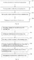
- FIG. 11 is a flow schematic chart of a packaging method according to Embodiment 6 of the present application.
- the packaging method according to this embodiment includes: Step 601: providing a channel set on a device area of a package base.
- step 601 in this embodiment refers to the description related to the step 401 in FIG. 9 , which will not be repeated here.
- Step 602 forming an insulating layer on the package base.
- a wafer may be also selected as the package base for illustration. Specifically, if an insulating layer on a surface of the wafer cannot meet the preset insulation standard and parasitism standard when the wafer leaves a factory, it is necessary to dispose an insulating layer on the wafer.
- the insulating layer may be formed on the wafer, where a layer of insulating layer may be formed on the surface of the wafer by means of uniform coating, plasma spraying, printing, film pasting and the like.
- Step 603 providing a window structure on the insulating layer.
- the photoetching process and the etching process may be used to form the window structure on the insulating layer, so as to expose the channel lead pad.
- the thickness of the insulating layer is usually in micron scale, for example, 5 microns.
- Step 604 forming a conductive medium layer on a side of the insulating layer away from the package base.
- a conductive medium layer may be further formed on the side of the insulating layer away from the wafer.
- the conductive medium layer may be formed by sputtering, vapor deposition, electroplating, chemical plating, pasting conductive film and other processes.
- the conductive medium layer is usually in micron scale, such as 1-8 microns.
- Step 605 patterning the conductive medium layer to form a redistribution layer.
- the conductive medium layer needs to be patterned to form the redistribution layer. It is worth noting that the conductive medium layer may be patterned by means of first photoresist coating, then photoetching, and then dry etching, or by means of first photoresist coating, then photoetching, and then wet etching, or by means of other patterning processes such as laser direct writing. In this embodiment, there is no limitation on a specific patterning process for the conductive medium layer.
- Step 606 packaging an electronic device on the device area.
- step 606 in this embodiment refers to the description of the step 504 in the embodiment shown in FIG. 10 , which will not be repeated here.
Landscapes
- Semiconductor Integrated Circuits (AREA)
- Engineering & Computer Science (AREA)
- Power Engineering (AREA)
- Physics & Mathematics (AREA)
- Geometry (AREA)
- Manufacturing & Machinery (AREA)
Abstract
Description
- The present application relates to the technical field of chip package, and in particular, to a package structure and a packaging method.
- With the development of science and technology, a requirement for a communication speed of a chip is getting higher and higher. Therefore, a higher requirement is put forward for a chip package structure.
- At present, in order to ensure the stability of performance and service life of a chip, every external channel of the chip must be provided with an electro-static discharge (Electro-Static discharge, ESD for short) protection circuit, so as to prevent static electricity from bringing instantaneous super charge inside the chip and causing static electricity damage to the chip.
- However, the ESD protection circuit may bring relatively great parasitism to the channel where the ESD protection circuit is located, and the parasitism of the ESD protection circuit during chip operation will seriously affect the communication speed of the chip.
- The present application provides a package structure and a packaging method, so as to realize electrostatic protection for a channel that needs to be protected in an electronic device during a packaging process of an electronic device, and reduce the parasitic influence of an ESD protection circuit on the electronic device after the packaging is finished.
- In a first aspect, the present application provides a package structure, including: a package base and a redistribution layer disposed on the package base;
where the package base includes a plurality of device areas; and
a channel set is provided in a device area, the channel set is used to connect an electronic device, and the redistribution layer is used to lead a subset of to-be-protected channels that needs electrostatic protection in the channel set out to a preset area on the package base, so that all or part of channels in the subset of to-be-protected channels form a series circuit in the preset area, where the series circuit is used to connect with an electrostatic discharge end. - In a possible design, the package base further includes: a device separation area set between adjacent device areas;
where the preset area is the device separation area, and the series circuit is disconnected during a separation operation on the device separation area; or,
the preset area is a partial area in the device area; and the series circuit is disconnected after a packaging operation of the electronic device is completed. - In a possible design, an insulating layer is provided on the package base; where
the insulating layer is provided with a window structure;
the redistribution layer is disposed on a side of the insulating layer away from the package base; and
the redistribution layer is connected with a channel in the channel set through the window structure. - In a possible design, a channel lead pad is provided on the package base, where the channel lead pad is used to establish a connection between the channel and the electronic device; and
the channel lead pad is connected with the redistribution layer through the window structure. - In a possible design, the package base is provided with a channel window, and the channel lead pad is disposed on the channel window, so as to establish a connection between the channel lead pad and the channel.
- In a possible design, the electrostatic discharge end is a grounding end or an electrostatic protection module port.
- In a possible design, the redistribution layer is made of a metal material or a non-metal conductive material.
- In a possible design, the redistribution layer is a single-layer structure or a multi-layer structure.
- In a possible design, the package base is a wafer, a substrate or a flexible circuit board.
- In a possible design, a protective coating is provided on the redistribution layer.
- In a second aspect, the present application further provides a packaging method, including:
- providing a redistribution layer and a channel set on a device area of a package base, where a subset of to-be-protected channels that needs electrostatic protection in the channel set is led out to a preset area on the package base through the redistribution layer, so that all or part of channels in the subset of to-be-protected channels form a series circuit in the preset area, where the series circuit is used to connect with an electrostatic discharge end; and
- packaging an electronic device on the device area, so as to establish a connection between the channel set and the electronic device.
- In a possible design, after packaging an electronic device on the device area, the packaging method further includes:
- performing a separation operation on a device separation area, so as to disconnect the series circuit, where the device separation area is set between adjacent device areas, and the preset area is the device separation area; or,
- disconnecting the series circuit by a disconnection process on the redistribution layer, where the preset area is a partial area in the device area.
- In a possible design, the providing a redistribution layer on a device area of a package base includes:
- forming an insulating layer on the package base;
- providing a window structure on the insulating layer; and
- forming the redistribution layer on a side of the insulating layer away from the package base; where the redistribution layer is connected with a channel in the channel set through the window structure.
- In a possible design, the forming the redistribution layer on the package base includes:
- forming a conductive medium layer; and
- patterning the conductive medium layer to form the redistribution layer.
- In a possible design, after forming the redistribution layer, the packaging method further includes:
forming a protective coating on the redistribution layer. - In a possible design, the electrostatic discharge end is a grounding end or an electrostatic protection module port.
- In a possible design, the redistribution layer is made of a metal material or a non-metal conductive material.
- In a possible design, the redistribution layer is a single-layer structure or a multi-layer structure.
- In a possible design, the package base is a wafer, a substrate or a flexible circuit board.
- In the package structure and the packaging method provided by the present application, a subset of to-be-protected channels that needs electrostatic protection in a channel set is led out to a preset area on a package base through a redistribution layer, so that all or part of channels in the subset of to-be-protected channels form a series circuit in the preset area and then connect with an electrostatic discharge end, thereby realizing electrostatic protection of the channel that needs to be protected.
- In order to more clearly explain the technical solutions of embodiments of the present application or the prior art, the following will make a brief introduction to the drawings used in the description of the embodiments or the prior art. Obviously, the drawings in the following description are some of the embodiments of the present application. Those skilled in the art can also obtain other drawings according to these drawings without creative efforts.
-
FIG. 1 is a schematic structural diagram of a package structure according to Embodiment 1 of the present application; -
FIG. 2 is a schematic structural diagram of a package base of a package structure according to Embodiment 2 of the present application; -
FIG. 3 is a schematic structural diagram of a conductive medium layer formed in the package structure according to Embodiment 2 of the present application; -
FIG. 4 is a schematic structural diagram of a redistribution layer formed in the package structure according to Embodiment 2 of the present application; -
FIG. 5 is a schematic structural diagram of an insulating layer formed in a package structure according to Embodiment 3 of the present application; -
FIG. 6 is a schematic structural diagram of a window structure formed in the package structure according to Embodiment 3 of the present application; -
FIG. 7 is a schematic structural diagram of a conductive medium layer formed in the package structure according to Embodiment 3 of the present application; -
FIG. 8 is a schematic structural diagram of a redistribution layer formed in the package structure according to Embodiment 3 of the present application; -
FIG. 9 is a schematic flowchart of a packaging method according to Embodiment 4 of the present application; -
FIG. 10 is a schematic flowchart of a packaging method according to Embodiment 5 of the present application; and -
FIG. 11 is a schematic flowchart of a packaging method according to Embodiment 6 of the present application. - Through the above drawings, specific embodiments of the present disclosure have been shown, which will be described in more detail in the following. These drawings and descriptions are not intended to limit the scope of the conception of the present disclosure in any way, but to illustrate the concepts of the present disclosure for those skilled in the art with reference to specific embodiments.
- In order to make purposes, technical solutions and advantages of embodiments of the present application clearer, the technical solutions in the embodiments of the present application will be described clearly and completely in combination with the drawings in the embodiments of the present application. Obviously, the described embodiments are a part of, not all of, the embodiments of the present application. On the basis of the embodiments of the present application, all of other embodiments obtained by those skilled in the art without creative efforts fall into the protection scope of the present application.
- The terms "first", "second", "third", "fourth" and the like (if any) in the description and the claims as well as the drawings of the present application are used to distinguish similar objects, rather than to describe a specific order or sequence. It should be understood that the data as used can be interchanged where appropriate so that the embodiments of the present application described herein can, for example, be implemented in a sequence other than those illustrated or described here. In addition, the terms "include" and "comprise" as well as any variation thereof are intended to refer to non-exclusive inclusion. For example, a process, a method, a system, a product or an apparatus including a series of steps or units is not necessarily limited to those steps or units clearly listed, but may include other steps or units that are not clearly listed or inherent to such process, method, product or apparatus.
- In combination with specific embodiments, the following describes in detail the technical solution of the present application and how the technical solution of the present application solves the above-mentioned technical problems. The following several specific embodiments can be combined with each other, and the same or similar concepts or processes may not be repeated in some embodiments. The embodiments of the present application will be described in combination with the drawings.
-
FIG. 1 is a schematic structural diagram of a package structure according to Embodiment 1 of the present application. As shown inFIG. 1 , the package structure provided in this embodiment includes: a package base and aredistribution layer 302 disposed on the package base. - Where the package base includes a plurality of
device areas 102. It is worth understanding that the package base may be a wafer, a substrate or a flexible circuit board, and there is no limitation on a specific form of the package base in this embodiment. In order to explain the principle of this embodiment in detail, awafer 101 may be selected as the package base for illustration. As for thedevice area 102, it may be a partial area on the package base, which is used to package a chip or any other device. - Moreover, a channel set is provided in the
device area 102, where the channel set in thedevice area 102 is used to connect an electronic device. It is worth understanding that a channel in the channel set here may be any connection channel in the package structure, which may be on thewafer 101, may be made by package processing, or may be on a substrate. - As for the
redistribution layer 302, it may be understood as a patterned conductive layer on a surface of thewafer 101, and can be used to rearrange the channel set on thedevice area 102. Theredistribution layer 302 may be a single-layer conductive layer structure or a multi-layer conductive layer structure. In this embodiment, there is no limitation on a specific layer number of theredistribution layer 302, and it is only necessary to ensure that a subset of to-be-protected channels that needs electrostatic protection in the channel set on thedevice area 102 can be led out to a preset area on thewafer 101 through theredistribution layer 302, so that all or part of channels in the subset of to-be-protected channels form a series circuit in the preset area. - In addition, it should be understood that the above channel set may be a channel lead pad on the
wafer 101, or may be a pad structure obtained by secondary packaging processing on the basis of the channel lead pad on theoriginal wafer 101, and additionally, it may also be a channel lead pad on another type of substrate or flexible circuit board. - It is worth noting that in a packaging process of an electronic device, for example, in a packaging process of a chip, external environment (such as equipment, materials, persons, etc.) may bring static electricity, which can easily cause instantaneous super charge inside the chip. Therefore, it is necessary to perform electrostatic discharge protection on a channel which is in the
device area 102 and is for establishing a connection with the chip. In the prior art, an individual ESD protection circuit is provided for each channel that needs to be protected, and after the package is finished and a chip module is formed through cutting, these ESD protection circuits are still parasitic on the channels. These parasitic ESD protection circuits consume power during the working of the chip module, and will cause reverse inductance when the chip module is working, thus reducing a driving voltage of each channel, thereby affecting the communication speed of the chip module. - In this embodiment, in order to be able to perform electrostatic protection on the channel that needs to be protected, all or part of channels in the subset of to-be-protected channels that needs electrostatic protection in the channel set may form a series circuit in a preset area of the
wafer 101 through theredistribution layer 302, and the series circuit may be connected with an electrostatic discharge end (such as an ESD protection module port or a ground wire). - Where, the preset area may be any position on the
wafer 101, which may be determined according to an actual packaging process and a layout form of the channel set. Specifically, the preset area may be an area outside thedevice area 102 or a partial area in the device area, and it is only necessary to ensure that after the package of the electronic device is finished, medium layer disconnection processing of the series circuit in the preset area will not affect the normal operation of the electronic device. - For example, the preset area may be a
device separation area 105 set betweenadjacent device areas 102. All or part of channels in the subset of to-be-protected channels that needs electrostatic protection in the channel set are led out to thedevice separation area 105 through theredistribution layer 302, and then all of the channels are connected in series or partially in series in thedevice separation area 105 to form a common potential. Then the series circuit is connected with an ESD protection module port or a ground wire to form a zero potential. In this way, when the chip is affected by electrostatic discharge, the electric charge will preferentially move to a lower potential, and all of the electric charges will be led away along the channel provided with the ESD protection circuit or the ground wire, thereby protecting a circuit inside the chip from the effect of the electrostatic discharge. Where, theredistribution layer 302 may be made of a metal material, such as aluminum, copper, nickel, palladium, gold, etc., and any conductive material such as a non-metal conductive material may also be used. - The
device separation area 105 may be an area formed by electronic device edges 103 of twoadjacent device areas 102, where thedevice separation area 105 may be a cutting channel between chips. After the package of the chip is finished, the chips are separated by a chip separation process. - It can be seen that the package structure according to this embodiment can reduce the effect of ESD on the chip during the packaging process. Moreover, when the packaging is finished, the chips will be cut into individual chip, and the series circuit formed in the cutting channel will be cut off by a cutting process, so that the channels separate again to restore the chip function. When the chip is subsequently loaded onto a board, the ESD protection for the chip will be continued by the board-level ESD protection process.
- For another example, the above preset area may also be a partial area in the
device area 102. Specifically, the preset area may be a middle part of thedevice area 102 or other areas where theredistribution layer 302 can be laid out. The preset area can be adaptively designed according to a specific arrangement of the channel set in thedevice area 102. Specifically, all or part of channels in the subset of to-be-protected channels that needs electrostatic protection in the channel set may be led out to a partial area in thedevice area 102 through theredistribution layer 302, and then all of the channels are connected in series or partially in series in the partial area of thedevice area 102 to form a common potential. Then the series circuit is connected with an ESD protection module port or a ground wire to form a zero potential. In this way, when the chip is affected by electrostatic discharge, the electric charge will preferentially move to a lower potential, and all of the electric charges will be led away along the channel provided with the ESD protection circuit or the ground wire, thereby protecting the circuit inside the chip from the effect of the electrostatic discharge. - After the packaging operation of the electronic device is finished, the series circuit may be disconnected by a conductive medium layer cutting process, such as laser cutting. Then, the
device areas 102 are sliced, and the chip are separated by a chip separation process. - It can be seen that the package structure according to this embodiment can reduce the effect of the ESD on the chip during the packaging process. Moreover, when the packaging is finished, the series circuit is disconnected by the conductive medium layer cutting process, so that the channels separate again to restore the chip function. When the chip is subsequently loaded onto a board, the ESD protection for the chip will be continued by the board-level ESD protection process.
- In the present embodiment, a subset of to-be-protected channels that needs electrostatic protection in a channel set is led out to a preset area on a package base through a redistribution layer, so that all or part of channels in the subset of to-be-protected channels form a series circuit in the preset area and then connect with the electrostatic discharge end, thereby realizing electrostatic protection of the channel that needs to be protected.
- In addition, after the package of the electronic device is finished, the channels may be separated again by disconnecting a multi-channel series circuit, so as to restore the chip function. It can be seen that a chip module obtained by slicing the package structure according to the embodiment can reduce or even avoid the parasitism of an ESD protection circuit on each channel of the chip, so as to effectively reduce power consumption during the working of the chip, and also improve the communication speed of the chip.
- In order to describe in detail the package structure according to the present application, a wafer may be selected as the package base, and a packaging method for the package structure may be combined for description.
-
FIG. 2 is a schematic structural diagram of a package base of a package structure according to Embodiment 2 of the present application. As shown inFIG. 2 , thewafer 101 includes a plurality ofdevice areas 102 and adevice separation area 105 set betweenadjacent device areas 102. - Moreover, a channel set is provided in the
device area 102, where the channel set in thedevice area 102 is used to connect an electronic device. It is worth understanding that a channel in the channel set here may be any connection channel in the package structure, for example, may be a channel used to package a chip to establish a connection with the chip. - The
wafer 101 is provided with achannel lead pad 104, where thechannel lead pad 104 is used to establish a connection between the channel and the electronic device. - The
device separation area 105 may be an area formed by electronic device edges 103 of twoadjacent device areas 102, where thedevice separation area 105 may be a cutting channel between chips. After the package of the chip is finished, the cutting channel is cut by a chip separation process to separate the chips. - It is worth noting that, referring to
FIG. 1 and FIG. 2 , it is necessary to confirm whether apad window 103 has been made for thechannel lead pad 104 before processing awafer 101. If a windowing process of an incoming material has been completed, thewafer 101 only needs a simple cleaning process and then can be used. If the windowing process of the incoming material has not been completed, a packaging factory needs to carry out the windowing process by a dry etching process or a wet etching process, so as to expose a metal pad. -
FIG. 3 is a schematic structure diagram of a conductive medium layer formed in the package structure according to Embodiment 2 of the present application. As shown inFIG. 3 , if an insulating layer on a surface of thewafer 101 can meet a preset insulation standard and parasitism standard when thewafer 101 leaves a factory, a conductivemedium layer 301 can be directly formed on thewafer 101. - It is worth noting that the conductive
medium layer 301 may be formed by sputtering, vapor deposition, electroplating, chemical plating, pasting conductive film and other processes. In this embodiment, there is no limitation on a specific forming process and material for the conductivemedium layer 301, as long as theoretical conductive requirements can be met. Optionally, the conductivemedium layer 301 is usually in micron scale, such as 1-8 microns. -
FIG. 4 is a schematic structure diagram of a redistribution layer formed in the package structure according to Embodiment 2 of the present application. As shown inFIG. 4 , after the conductive medium layer is formed, the conductivemedium layer 301 needs to be patterned to form theredistribution layer 302. It is worth noting that the conductivemedium layer 301 may be patterned by means of first photoresist coating, then photoetching, and then dry etching, or by means of first photoresist coating, then photoetching, and then wet etching, or by means of other patterning processes such as laser direct writing. In this embodiment, there is no limitation on a specific patterning process for the conductivemedium layer 301. - Referring to
FIG. 1 again, theredistribution layer 302 formed by a patterning process can lead all or part of channels in the channel set to thedevice separation area 105 to form a series circuit, and the series circuit is then connected with an electrostatic discharge end (for example, a channel provided with an ESD protection circuit or a ground wire). Therefore, all of the channels that need ESD protection are led to thedevice separation area 105, and then all of the channels are connected in series or partially in series in thedevice separation area 105 to form a common potential. Then the series circuit is connected with the channel with ESD protection or the ground wire to form a zero potential. In this way, when the chip is affected by electrostatic discharge, the electric charge will preferentially move to a lower potential, and all of the electric charges will be led away along the channel provided with the ESD protection circuit or the ground wire, thereby protecting the circuit inside the chip from the effect of the electrostatic discharge. -
FIG. 5 is a schematic structure diagram of an insulating layer formed in the package structure according to Embodiment 3 of the present application. Referring toFIG. 2 andFIG. 5 , if an insulating layer on a surface of awafer 101 cannot meet a preset insulation standard and parasitism standard when thewafer 101 leaves the factory, it is necessary to provide aninsulating layer 201 on thewafer 101. - Specifically, the insulating
layer 201 may be formed on thewafer 101, where a layer of insulatinglayer 201 may be formed on the surface of thewafer 101 by means of uniform coating, plasma spraying, printing, film pasting and the like. -
FIG. 6 is a schematic structure diagram of a window structure formed in the package structure according to Embodiment 3 of the present application. As shown inFIG. 6 , in order to form an effective connection, after the insulatinglayer 201 is formed, it is necessary to provide awindow structure 202 on the insulating layer. - Specifically, as for the forming process of the
window structure 202, a photoetching process and an etching process may be used to form thewindow structure 202 on the insulatinglayer 201, so as to expose thechannel lead pad 104. - In addition, it is worth noting that there is no specific limitation on the forming process of the insulating
layer 201 and thewindow structure 202, and there is also no specific limitation on the material of the insulating layer 20, as long as it is ensured that the surface of thedevice area 102 can be insulated, and thechannel lead pad 104 can be exposed. Optionally, the thickness of the insulatinglayer 201 is usually in micron scale, for example, 5 microns. -
FIG. 7 is a schematic structure diagram of a conductive medium layer formed in the package structure according to Embodiment 3 of the present application. As shown inFIG. 7 , after the insulatinglayer 201 is formed on thewafer 101 and thewindow structure 202 is formed, a conductivemedium layer 301 may be further formed on a side of the insulatinglayer 201 away from thewafer 101. - It is worth noting that the conductive
medium layer 301 may be formed by sputtering, vapor deposition, electroplating, chemical plating, pasting conductive film and other processes. In this embodiment, there is no limitation on a specific forming process and material for the conductivemedium layer 301, as long as theoretical conductive requirements can be met. Optionally, the conductivemedium layer 301 is usually in micron scale, such as 1-8 microns. -
FIG. 8 is a schematic structure diagram of a redistribution layer formed in the package structure according to Embodiment 3 of the present application. As shown inFIG. 8 , after the conductive medium layer is formed, the conductivemedium layer 301 needs to be patterned to form theredistribution layer 302. It is worth noting that the conductivemedium layer 301 may be patterned by means of first photoresist coating, then photoetching, and then dry etching, or by means of first photoresist coating, then photoetching, and then wet etching, or by means of other patterning processes such as laser direct writing. In this embodiment, there is no limitation on a specific patterning process for the conductivemedium layer 301. - Referring to
FIG. 1 again, theredistribution layer 302 formed by a patterning process can lead all or part of channels in the channel set to thedevice separation area 105 to form a series circuit, and the series circuit is then connected with an electrostatic discharge end (for example, a channel provided with an ESD protection circuit or a ground wire). Therefore, all of the channels that need ESD protection are led to thedevice separation area 105, and then all of the channels are connected in series or partially in series in thedevice separation area 105 to form a common potential. Then the series circuit is connected with the channel with ESD protection or the ground wire to form a zero potential. In this way, when the chip is affected by electrostatic discharge, the electric charge will preferentially move to a lower potential, and all of the electric charges will be led away along the channel provided with the ESD protection circuit or the ground wire, thereby protecting the circuit inside the chip from the effect of the electrostatic discharge. - On the basis of the above embodiments, in order to protect the formed
redistribution layer 302, a protective coating may be further provided on theredistribution layer 302, and then whether to make a window for the protective coating and a subsequent process can be set according to actual packaging requirements. -
FIG. 9 is a schematic flowchart of a packaging method according to Embodiment 4 of the present application. As shown inFIG. 9 , the packaging method according to this embodiment includes:
Step 401: providing a channel set on a device area of a package base. - The package base includes a plurality of device areas. It is worth understanding that the package base may be a wafer, a substrate or a flexible circuit board, and there is no limitation on a specific form of the package base in this embodiment. In order to explain principle of this embodiment in detail, a wafer may be selected as the package base for illustration. As for the device area, it may be a partial area on the package base, which is used to package a chip or any other device.
- Specifically, a channel set is provided in the device area, where the channel set in the device area is used to connect an electronic device. It is worth understanding that a channel in the channel set here may be any connection channel in the package structure, which may be on the wafer, may be made by package processing, or may be on the substrate.
- Optionally, the above channel set may be a channel lead pad on the wafer, or may be a pad structure obtained by secondary packaging processing on the basis of the channel lead pad on the original wafer, and additionally, it may also be a channel lead pad on another type of substrate or flexible circuit board.
- Step 402: providing a redistribution layer on the device area of the package base.
- Specifically, as for the redistribution layer, it may be understood as a patterned conductive layer on a surface of the wafer, and can be used to rearrange the channel set on the device area. The redistribution layer may be a single-layer conductive layer structure or a multi-layer conductive layer structure. In this embodiment, there is no limitation on a specific layer number of the redistribution layer, and it is only necessary to ensure that a subset of to-be-protected channels that needs electrostatic protection in the channel set on the device area can be led out to a preset area on the wafer through the redistribution layer, so that all or part of channels in the subset of to-be-protected channels form a series circuit in the preset area.
- Step 403: packaging an electronic device on the device area.
- After the redistribution layer is provided on the device area of the package base, an electronic device can be packaged on the device area.
- In a packaging process of the electronic device, for example, in a packaging process of a chip, external environment (such as equipment, materials, persons, etc.) may bring static electricity, which can easily cause instantaneous super charge inside the chip. Therefore, it is necessary to perform electrostatic discharge protection on a channel which is in the
device area 102 and is for establishing a connection with the chip. In the prior art, an individual ESD protection circuit is provided for each channel that needs to be protected, and after the package is finished and a chip module is formed through cutting, these ESD protection circuits are still parasitic on the channels. These parasitic ESD protection circuits consume power during the working of the chip module, and will cause reverse inductance when the chip module is working, thus reducing a driving voltage of each channel, thereby affecting the communication speed of the chip module. - In this embodiment, in order to be able to perform electrostatic protection on the channel that needs to be protected, all or part of channels in the subset of to-be-protected channels that needs electrostatic protection in the channel set may form a series circuit in a preset area of the wafer through the redistribution layer, and the series circuit may be connected with an electrostatic discharge end (such as an ESD protection module port or a ground wire).
-
FIG. 10 is a schematic flowchart diagram of a packaging method according to Embodiment 5 of the present application. As shown inFIG. 10 , the packaging method according to this embodiment includes:
Step 501: providing a channel set on a device area of a package base. - It is worth noting that the specific description of the
step 501 in this embodiment refers to the description related to thestep 401 inFIG. 9 , which will not be repeated here. - Step 502: forming a conductive medium layer on the package base.
- The package base includes a plurality of device areas and a device separation area set between adjacent device areas. It is worth understanding that the package base may be a wafer, a substrate or a flexible circuit board, and there is no limitation on a specific form of the package base in this embodiment. In order to explain principles in the embodiment in detail, a wafer may be selected as the package base for illustration.
- Specifically, the wafer includes a plurality of device areas and a device separation area set between adjacent device areas.
- Moreover, a channel set is provided in the device area, where the channel set in the device area is used to connect an electronic device. It is worth understanding that a channel in the channel set here may be any connection channel in the package structure, for example, may be a channel used to package a chip to establish a connection with the chip.
- The wafer is provided with a channel lead pad, where the channel lead pad is used to establish a connection between the channel and the electronic device.
- The device separation area may be an area formed by electronic device edges of two adjacent device areas, where the device separation area may be a cutting channel between chips. After the package of the chip is finished, the cutting channel is cut by a chip separation process to separate the chips.
- If an insulating layer on a surface of the wafer can meet a preset insulation standard and parasitism standard when the wafer leaves a factory, a conductive medium layer can be directly formed on the wafer.
- It is worth noting that the conductive medium layer may be formed by sputtering, vapor deposition, electroplating, chemical plating, pasting conductive film and other processes. In this embodiment, there is no limitation on a specific forming process and material for the conductive medium layer, as long as theoretical conductive requirements can be met. Optionally, the conductive medium layer is usually in micron scale, such as 1-8 microns.
- Step 503: patterning the conductive medium layer to form a redistribution layer.
- After the conductive medium layer is formed, the conductive medium layer needs to be patterned to form the redistribution layer. It is worth noting that the conductive medium layer may be patterned by means of first photoresist coating, then photoetching, and then dry etching, or by means of first photoresist coating, then photoetching, and then wet etching, or by means of other patterning processes such as laser direct writing. In this embodiment, there is no limitation on a specific patterning process for the conductive medium layer.
- Step 504: packaging an electronic device on the device area.
- The redistribution layer formed by a patterning process can lead all or part of channels in the subset of to-be-protected channels that needs electrostatic protection in the channel set out to the preset area of the package base to form a series circuit.
- Where, the above preset area may be any position on the package base, which may be determined according to an actual packaging process and a layout form of the channel set. Specifically, the preset area may be an area outside the device area or a partial area in the device area, and it is only necessary to ensure that after the package of the electronic device is finished, medium layer disconnection processing of the series circuit in the preset area will not affect the normal operation of the electronic device.
- For example, the preset area may be a device separation area set between
adjacent device areas 102. All or part of channels in the subset of to-be-protected channels that needs electrostatic protection in the channel set are led out to the device separation area through the redistribution layer, and then all of the channels are connected in series or partially in series in thedevice separation area 105 to form a common potential. Then the series circuit is connected with an ESD protection module port or a ground wire to form a zero potential. In this way, when the chip is affected by electrostatic discharge, the electric charge will preferentially move to a lower potential, and all of the electric charges will be led away along the channel provided with the ESD protection circuit or the ground wire, thereby protecting a circuit inside the chip from the effect of the electrostatic discharge. Where, theredistribution layer 302 may be made of a metal material, such as aluminum, copper, nickel, palladium, gold, etc., and any conductive material such as a non-metal conductive material may also be used. - For another example, the above preset area may also be a partial area in the device area. Specifically, the preset area may be a middle part of the device area or other areas where the redistribution layer can be laid out. The preset area can be adaptively designed according to a specific arrangement of the channel set in the device area. All or part of channels in the subset of to-be-protected channels that needs electrostatic protection in the channel set may be led out to a partial area in the device area through the redistribution layer, and then all of the channels are connected in series or partially in series in the partial area of the device area to form a common potential. Then the series circuit is connected with an ESD protection module port or a ground wire to form a zero potential. In this way, when the chip is affected by electrostatic discharge, the electric charge will preferentially move to a lower potential, and all of the electric charges will be led away along the channel provided with the ESD protection circuit or the ground wire, thereby protecting the circuit inside the chip from the effect of the electrostatic discharge.
- In this embodiment, by forming the redistribution layer, the subset of to-be-protected channels that needs electrostatic protection in the channel set can be led out to the preset area of the package base, so that all or part of channels in the subset of to-be-protected channels form a series circuit in the preset area and then connect with the electrostatic discharge end, thereby realizing electrostatic protection of the channel that needs to be protected.
- On the basis of the above Embodiment 4, in order to slice the package structure obtained by the above embodiment to obtain a chip module, and ensure that the sliced chip module can work normally, after the package of the electronic device is finished, it is also necessary to disconnect the series circuit formed by all or part of channels in the subset of to-be-protected channels in the preset area.
- Specifically, when the above preset area is a device separation area, the device separation area can be set as a cutting channel between chips. After the package of the chip is finished, the chips are separated by a chip separation process. When the packaging is finished, the chips will be cut into individual chips, and the series circuit formed in the cutting channel will be cut off by a cutting process, so that the channels separate again to restore the chip function. When the chip is subsequently loaded onto a board, the ESD protection for the chip will be continued by the board-level ESD protection process.
- In addition, when the above preset area is a partial area in the device area, after the package of the electronic device is finished, the series circuit may be disconnected by a conductive medium layer cutting process, such as laser cutting. Then, the device areas are sliced, and the chips are separated by the chip separation process.
- It can be seen that in this embodiment, the series circuit for electrostatic protection is disconnected to separate the channels again, so as to restore the chip function. It can be seen that the package structure according to this embodiment can reduce or even avoid the parasitism of the ESD protection circuit on each channel, so as to effectively reduce power consumption during the working of the chip, and also improve the communication speed of the chip.
-
FIG. 11 is a flow schematic chart of a packaging method according to Embodiment 6 of the present application. As shown inFIG. 11 , the packaging method according to this embodiment includes:
Step 601: providing a channel set on a device area of a package base. - It is worth noting that the specific description of the
step 601 in this embodiment refers to the description related to thestep 401 inFIG. 9 , which will not be repeated here. - Step 602: forming an insulating layer on the package base.
- A wafer may be also selected as the package base for illustration. Specifically, if an insulating layer on a surface of the wafer cannot meet the preset insulation standard and parasitism standard when the wafer leaves a factory, it is necessary to dispose an insulating layer on the wafer.
- Specifically, the insulating layer may be formed on the wafer, where a layer of insulating layer may be formed on the surface of the wafer by means of uniform coating, plasma spraying, printing, film pasting and the like.
- Step 603: providing a window structure on the insulating layer.
- In order to form an effective connection, after the insulating layer is formed, it is necessary to provide a window structure on the insulating layer.
- Specifically, as for the forming process of the window structure, the photoetching process and the etching process may be used to form the window structure on the insulating layer, so as to expose the channel lead pad.
- In addition, it is worth noting that there is no specific limitation on the forming process of the insulating layer and the window structure, and there is also no specific limitation on the material of the insulating layer, as long as it is ensured that the surface of the device area can be insulated, and the channel lead pad can be exposed. Optionally, the thickness of the insulating layer is usually in micron scale, for example, 5 microns.
- Step 604: forming a conductive medium layer on a side of the insulating layer away from the package base.
- After the insulating layer is formed on the wafer and the window structure is formed, a conductive medium layer may be further formed on the side of the insulating layer away from the wafer.
- It is worth noting that the conductive medium layer may be formed by sputtering, vapor deposition, electroplating, chemical plating, pasting conductive film and other processes. In this embodiment, there is no limitation on a specific forming process and material for the conductive medium layer, as long as theoretical conductive requirements can be met. Optionally, the conductive medium layer is usually in micron scale, such as 1-8 microns.
- Step 605: patterning the conductive medium layer to form a redistribution layer.
- After the conductive medium layer is formed, the conductive medium layer needs to be patterned to form the redistribution layer. It is worth noting that the conductive medium layer may be patterned by means of first photoresist coating, then photoetching, and then dry etching, or by means of first photoresist coating, then photoetching, and then wet etching, or by means of other patterning processes such as laser direct writing. In this embodiment, there is no limitation on a specific patterning process for the conductive medium layer.
- Step 606: packaging an electronic device on the device area.
- It is worth noting that the specific implementation of the
step 606 in this embodiment refers to the description of thestep 504 in the embodiment shown inFIG. 10 , which will not be repeated here. - Those skilled in the art will easily think of other implementations of the present disclosure after considering the description and practicing the application disclosed herein. The present application is intended to cover any variations, uses or adaptive changes of the present disclosure, and these variations, uses or adaptive changes follow general principles of the present disclosure and include common knowledge or conventional technical means in the technical field that is not disclosed in the present disclosure. The description and the embodiments are only regarded as illustrative, and the true scope and spirit of the present disclosure are pointed out by the following claims.
- It should be understood that the present disclosure is not limited to the precise structures already described above and shown in the drawings, and various modifications and changes may be made without departing from the scope thereof. The scope of the present disclosure is only limited by the claims.
Claims (19)
- A package structure, comprising: a package base and a redistribution layer disposed on the package base;
wherein the package base comprises a plurality of device areas; and
a channel set is provided in a device area, the channel set is used to connect an electronic device, and the redistribution layer is used to lead a subset of to-be-protected channels that needs electrostatic protection in the channel set out to a preset area on the package base, so that all or part of channels in the subset of to-be-protected channels form a series circuit in the preset area, wherein the series circuit is used to connect with an electrostatic discharge end. - The package structure according to claim 1, wherein the package base further comprises: a device separation area set between adjacent device areas;
wherein the preset area is the device separation area, and the series circuit is disconnected during a separation operation on the device separation area; or,
the preset area is a partial area in the device area; and the series circuit is disconnected after a packaging operation of the electronic device is completed. - The package structure according to claim 1 or 2, wherein an insulating layer is provided on the package base; wherein
the insulating layer is provided with a window structure;
the redistribution layer is disposed on a side of the insulating layer away from the package base; and
the redistribution layer is connected with a channel in the channel set through the window structure. - The package structure according to claim 3, wherein a channel lead pad is provided on the package base, wherein the channel lead pad is used to establish a connection between the channel and the electronic device; and
the channel lead pad is connected with the redistribution layer through the window structure. - The package structure according to claim 4, wherein the package base is provided with a channel window, and the channel lead pad is disposed on the channel window, so as to establish a connection between the channel lead pad and the channel.
- The package structure according to claim 1 or 2, wherein the electrostatic discharge end is a grounding end or an electrostatic protection module port.
- The package structure according to claim 1 or 2, wherein the redistribution layer is made of a metal material or a non-metal conductive material.
- The package structure according to claim 1 or 2, wherein the redistribution layer is a single-layer structure or a multi-layer structure.
- The package structure according to claim 1 or 2, wherein the package base is a wafer, a substrate or a flexible circuit board.
- The package structure according to claim 1 or 2, wherein a protective coating is provided on the redistribution layer.
- A packaging method, comprising:providing a channel set and a redistribution layer on a device area of a package base, wherein a subset of to-be-protected channels that needs electrostatic protection in the channel set is led out to a preset area on the package base through the redistribution layer, so that all or part of channels in the subset of to-be-protected channels form a series circuit in the preset area, wherein the series circuit is used to connect with an electrostatic discharge end; andpackaging an electronic device on the device area, so as to establish a connection between the channel set and the electronic device.
- The packaging method according to claim 11, wherein after packaging an electronic device on the device area, the packaging method further comprises:performing a separation operation on a device separation area, so as to disconnect the series circuit, wherein the device separation area is set between adjacent device areas, and the preset area is the device separation area; or,disconnecting the series circuit by a disconnection process on the redistribution layer, wherein the preset area is a partial area in the device area.
- The packaging method according to claim 11 or 12, wherein the providing a redistribution layer on a device area of a package base comprises:forming an insulating layer on the package base;providing a window structure on the insulating layer; andforming the redistribution layer on a side of the insulating layer away from the package base; wherein the redistribution layer is connected with a channel in the channel set through the window structure.
- The packaging method according to claim 13, wherein the forming the redistribution layer on the package base comprises:forming a conductive medium layer; andpatterning the conductive medium layer to form the redistribution layer.
- The packaging method according to claim 14, wherein after forming the redistribution layer, the packaging method further comprises:
forming a protective coating on the redistribution layer. - The packaging method according to claim 11 or 12, wherein the electrostatic discharge end is a grounding end or an electrostatic protection module port.
- The packaging method according to claim 11 or 12, wherein the redistribution layer is made of a metal material or a non-metal conductive material.
- The packaging method according to claim 11 or 12, wherein the redistribution layer is a single-layer structure or a multi-layer structure.
- The packaging method according to claim 11 or 12, wherein the package base is a wafer, a substrate or a flexible circuit board.
Applications Claiming Priority (1)
| Application Number | Priority Date | Filing Date | Title |
|---|---|---|---|
| PCT/CN2019/089832 WO2020243880A1 (en) | 2019-06-03 | 2019-06-03 | Packaging structure and packaging method |
Publications (2)
| Publication Number | Publication Date |
|---|---|
| EP3799119A1 true EP3799119A1 (en) | 2021-03-31 |
| EP3799119A4 EP3799119A4 (en) | 2021-08-25 |
Family
ID=70306520
Family Applications (1)
| Application Number | Title | Priority Date | Filing Date |
|---|---|---|---|
| EP19931580.5A Pending EP3799119A4 (en) | 2019-06-03 | 2019-06-03 | ENCAPSULATION STRUCTURE AND ENCAPSULATION PROCESS |
Country Status (5)
| Country | Link |
|---|---|
| US (1) | US11646278B2 (en) |
| EP (1) | EP3799119A4 (en) |
| KR (1) | KR20210013141A (en) |
| CN (1) | CN111066143B (en) |
| WO (1) | WO2020243880A1 (en) |
Family Cites Families (10)
| Publication number | Priority date | Publication date | Assignee | Title |
|---|---|---|---|---|
| JP3427352B2 (en) * | 1999-08-24 | 2003-07-14 | アムコー テクノロジー コリア インコーポレーティド | Circuit board for semiconductor package |
| US7859098B2 (en) * | 2006-04-19 | 2010-12-28 | Stats Chippac Ltd. | Embedded integrated circuit package system |
| TWI341580B (en) * | 2007-06-05 | 2011-05-01 | Siliconware Precision Industries Co Ltd | Metohod for fabricating semiconductor device installed with passive components |
| CN101325164A (en) * | 2007-06-12 | 2008-12-17 | 矽品精密工业股份有限公司 | Method for fabricating semiconductor device connected with passive device |
| US8183593B2 (en) * | 2009-10-16 | 2012-05-22 | Oracle America, Inc. | Semiconductor die with integrated electro-static discharge device |
| CN103531580B (en) * | 2012-07-06 | 2016-08-03 | 联咏科技股份有限公司 | Chip package structure |
| US8896094B2 (en) * | 2013-01-23 | 2014-11-25 | Taiwan Semiconductor Manufacturing Company, Ltd. | Methods and apparatus for inductors and transformers in packages |
| US9960227B2 (en) * | 2013-09-11 | 2018-05-01 | Xilinx, Inc. | Removal of electrostatic charges from interposer for die attachment |
| CN205486157U (en) * | 2015-12-31 | 2016-08-17 | 茂丞科技股份有限公司 | fingerprint identification device |
| CN109449140B (en) * | 2018-10-31 | 2020-09-11 | 昆山国显光电有限公司 | Display panel and motherboard |
-
2019
- 2019-06-03 CN CN201980004135.6A patent/CN111066143B/en active Active
- 2019-06-03 EP EP19931580.5A patent/EP3799119A4/en active Pending
- 2019-06-03 WO PCT/CN2019/089832 patent/WO2020243880A1/en not_active Ceased
- 2019-06-03 KR KR1020207036736A patent/KR20210013141A/en not_active Ceased
-
2020
- 2020-12-28 US US17/134,748 patent/US11646278B2/en active Active
Also Published As
| Publication number | Publication date |
|---|---|
| US20210118825A1 (en) | 2021-04-22 |
| CN111066143B (en) | 2023-01-24 |
| EP3799119A4 (en) | 2021-08-25 |
| US11646278B2 (en) | 2023-05-09 |
| WO2020243880A1 (en) | 2020-12-10 |
| CN111066143A (en) | 2020-04-24 |
| KR20210013141A (en) | 2021-02-03 |
Similar Documents
| Publication | Publication Date | Title |
|---|---|---|
| US7476563B2 (en) | Method of packaging a device using a dielectric layer | |
| EP3125281B1 (en) | Semiconductor device and method of encapsulating semiconductor die | |
| US5930098A (en) | Multichip semiconductor structures with interchip electrostatic discharge protection, and fabrication methods therefore | |
| US7894172B2 (en) | ESD protection structure | |
| US9824955B2 (en) | Semiconductor device | |
| US20150187705A1 (en) | Semiconductor package having emi shielding and method of fabricating the same | |
| CN102171824A (en) | Electrostatic discharge (ESD) shielding for stacked ICs | |
| KR102548550B1 (en) | Semiconductor package and method for manufacturing the semiconductor package | |
| CN108288614B (en) | Method for manufacturing semiconductor device chip | |
| CN102289115A (en) | Method for manufacturing master board and TFT (Thin Film Transistor) array substrate | |
| WO2014132939A1 (en) | Semiconductor device | |
| KR20160046369A (en) | Semiconductor package | |
| US9252139B2 (en) | Stacked semiconductor package and method for manufacturing the same | |
| US11646278B2 (en) | Package structure and packaging method | |
| US7170361B1 (en) | Method and apparatus of interposing voltage reference traces between signal traces in semiconductor devices | |
| US20080203545A1 (en) | Semiconductor device and method of fabrication thereof | |
| CN209929300U (en) | Package structure | |
| CN101271874B (en) | Semiconductor element with noise suppression function and manufacturing method thereof | |
| CN115911003A (en) | Driver chip and manufacturing method thereof, display module | |
| CN103383920B (en) | The passivation of wafer level chip scale package device | |
| US8293640B2 (en) | Semiconductor structure and manufacturing method thereof | |
| US20110084394A1 (en) | Semiconductor Structure | |
| CN210042372U (en) | An FPC with anti-static structure | |
| KR20200025293A (en) | semiconductor device and a method of fabricating the same | |
| CN102254857B (en) | Semiconductor technology and structure |
Legal Events
| Date | Code | Title | Description |
|---|---|---|---|
| STAA | Information on the status of an ep patent application or granted ep patent |
Free format text: STATUS: THE INTERNATIONAL PUBLICATION HAS BEEN MADE |
|
| PUAI | Public reference made under article 153(3) epc to a published international application that has entered the european phase |
Free format text: ORIGINAL CODE: 0009012 |
|
| STAA | Information on the status of an ep patent application or granted ep patent |
Free format text: STATUS: REQUEST FOR EXAMINATION WAS MADE |
|
| 17P | Request for examination filed |
Effective date: 20201222 |
|
| AK | Designated contracting states |
Kind code of ref document: A1 Designated state(s): AL AT BE BG CH CY CZ DE DK EE ES FI FR GB GR HR HU IE IS IT LI LT LU LV MC MK MT NL NO PL PT RO RS SE SI SK SM TR |
|
| AX | Request for extension of the european patent |
Extension state: BA ME |
|
| A4 | Supplementary search report drawn up and despatched |
Effective date: 20210723 |
|
| RIC1 | Information provided on ipc code assigned before grant |
Ipc: H01L 21/78 20060101AFI20210719BHEP Ipc: H01L 23/60 20060101ALI20210719BHEP Ipc: H01L 23/485 20060101ALI20210719BHEP Ipc: H01L 23/00 20060101ALI20210719BHEP Ipc: H01L 23/498 20060101ALN20210719BHEP |
|
| DAV | Request for validation of the european patent (deleted) | ||
| DAX | Request for extension of the european patent (deleted) |