EP3797181B1 - Copper strip for producing electrical contacts and method for producing a copper strip and plug-in connector - Google Patents
Copper strip for producing electrical contacts and method for producing a copper strip and plug-in connector Download PDFInfo
- Publication number
- EP3797181B1 EP3797181B1 EP19726624.0A EP19726624A EP3797181B1 EP 3797181 B1 EP3797181 B1 EP 3797181B1 EP 19726624 A EP19726624 A EP 19726624A EP 3797181 B1 EP3797181 B1 EP 3797181B1
- Authority
- EP
- European Patent Office
- Prior art keywords
- coating
- phase
- copper strip
- copper
- tin
- Prior art date
- Legal status (The legal status is an assumption and is not a legal conclusion. Google has not performed a legal analysis and makes no representation as to the accuracy of the status listed.)
- Active
Links
- 239000010949 copper Substances 0.000 title claims description 72
- 229910052802 copper Inorganic materials 0.000 title claims description 72
- RYGMFSIKBFXOCR-UHFFFAOYSA-N Copper Chemical compound [Cu] RYGMFSIKBFXOCR-UHFFFAOYSA-N 0.000 title claims description 71
- 238000004519 manufacturing process Methods 0.000 title claims description 8
- 238000000576 coating method Methods 0.000 claims description 79
- 239000011248 coating agent Substances 0.000 claims description 78
- ATJFFYVFTNAWJD-UHFFFAOYSA-N Tin Chemical compound [Sn] ATJFFYVFTNAWJD-UHFFFAOYSA-N 0.000 claims description 48
- 229910052718 tin Inorganic materials 0.000 claims description 48
- 229910017692 Ag3Sn Inorganic materials 0.000 claims description 41
- 239000000463 material Substances 0.000 claims description 41
- 238000000034 method Methods 0.000 claims description 35
- 230000008569 process Effects 0.000 claims description 29
- 229910052709 silver Inorganic materials 0.000 claims description 27
- 239000004332 silver Substances 0.000 claims description 27
- 229910018471 Cu6Sn5 Inorganic materials 0.000 claims description 20
- 229910000881 Cu alloy Inorganic materials 0.000 claims description 16
- PXHVJJICTQNCMI-UHFFFAOYSA-N Nickel Chemical compound [Ni] PXHVJJICTQNCMI-UHFFFAOYSA-N 0.000 claims description 12
- 238000007598 dipping method Methods 0.000 claims description 11
- 238000009713 electroplating Methods 0.000 claims description 9
- 239000002245 particle Substances 0.000 claims description 8
- 229910017052 cobalt Inorganic materials 0.000 claims description 5
- 239000010941 cobalt Substances 0.000 claims description 5
- GUTLYIVDDKVIGB-UHFFFAOYSA-N cobalt atom Chemical compound [Co] GUTLYIVDDKVIGB-UHFFFAOYSA-N 0.000 claims description 5
- 229910052732 germanium Inorganic materials 0.000 claims description 5
- GNPVGFCGXDBREM-UHFFFAOYSA-N germanium atom Chemical compound [Ge] GNPVGFCGXDBREM-UHFFFAOYSA-N 0.000 claims description 5
- 229910052759 nickel Inorganic materials 0.000 claims description 5
- 229910052787 antimony Inorganic materials 0.000 claims description 4
- WATWJIUSRGPENY-UHFFFAOYSA-N antimony atom Chemical compound [Sb] WATWJIUSRGPENY-UHFFFAOYSA-N 0.000 claims description 4
- 229910052797 bismuth Inorganic materials 0.000 claims description 4
- JCXGWMGPZLAOME-UHFFFAOYSA-N bismuth atom Chemical compound [Bi] JCXGWMGPZLAOME-UHFFFAOYSA-N 0.000 claims description 4
- BQCADISMDOOEFD-UHFFFAOYSA-N Silver Chemical group [Ag] BQCADISMDOOEFD-UHFFFAOYSA-N 0.000 description 26
- 230000015572 biosynthetic process Effects 0.000 description 19
- 229910018082 Cu3Sn Inorganic materials 0.000 description 17
- 230000032683 aging Effects 0.000 description 15
- 238000001816 cooling Methods 0.000 description 14
- 238000009792 diffusion process Methods 0.000 description 10
- 230000000694 effects Effects 0.000 description 10
- 239000011148 porous material Substances 0.000 description 9
- 238000007792 addition Methods 0.000 description 8
- 239000000853 adhesive Substances 0.000 description 8
- 230000001070 adhesive effect Effects 0.000 description 8
- 230000008901 benefit Effects 0.000 description 6
- 230000009466 transformation Effects 0.000 description 6
- 239000002244 precipitate Substances 0.000 description 4
- 238000007669 thermal treatment Methods 0.000 description 3
- 230000002411 adverse Effects 0.000 description 2
- 230000004888 barrier function Effects 0.000 description 2
- 238000005260 corrosion Methods 0.000 description 2
- 230000007797 corrosion Effects 0.000 description 2
- 230000001419 dependent effect Effects 0.000 description 2
- 238000011161 development Methods 0.000 description 2
- 230000018109 developmental process Effects 0.000 description 2
- 230000002349 favourable effect Effects 0.000 description 2
- 230000006872 improvement Effects 0.000 description 2
- 230000013011 mating Effects 0.000 description 2
- 230000008092 positive effect Effects 0.000 description 2
- 238000001556 precipitation Methods 0.000 description 2
- 239000000047 product Substances 0.000 description 2
- XLYOFNOQVPJJNP-UHFFFAOYSA-N water Substances O XLYOFNOQVPJJNP-UHFFFAOYSA-N 0.000 description 2
- 229910017755 Cu-Sn Inorganic materials 0.000 description 1
- 229910017927 Cu—Sn Inorganic materials 0.000 description 1
- 238000005299 abrasion Methods 0.000 description 1
- 229910045601 alloy Inorganic materials 0.000 description 1
- 239000000956 alloy Substances 0.000 description 1
- 238000005275 alloying Methods 0.000 description 1
- 230000001609 comparable effect Effects 0.000 description 1
- KUNSUQLRTQLHQQ-UHFFFAOYSA-N copper tin Chemical compound [Cu].[Sn] KUNSUQLRTQLHQQ-UHFFFAOYSA-N 0.000 description 1
- 239000013078 crystal Substances 0.000 description 1
- 238000005538 encapsulation Methods 0.000 description 1
- 230000002401 inhibitory effect Effects 0.000 description 1
- 230000005764 inhibitory process Effects 0.000 description 1
- 239000007788 liquid Substances 0.000 description 1
- 239000002184 metal Substances 0.000 description 1
- 229910052751 metal Inorganic materials 0.000 description 1
- 230000004048 modification Effects 0.000 description 1
- 238000012986 modification Methods 0.000 description 1
- 230000002093 peripheral effect Effects 0.000 description 1
- 238000001953 recrystallisation Methods 0.000 description 1
- 238000003878 thermal aging Methods 0.000 description 1
Images

Classifications
-
- C—CHEMISTRY; METALLURGY
- C23—COATING METALLIC MATERIAL; COATING MATERIAL WITH METALLIC MATERIAL; CHEMICAL SURFACE TREATMENT; DIFFUSION TREATMENT OF METALLIC MATERIAL; COATING BY VACUUM EVAPORATION, BY SPUTTERING, BY ION IMPLANTATION OR BY CHEMICAL VAPOUR DEPOSITION, IN GENERAL; INHIBITING CORROSION OF METALLIC MATERIAL OR INCRUSTATION IN GENERAL
- C23C—COATING METALLIC MATERIAL; COATING MATERIAL WITH METALLIC MATERIAL; SURFACE TREATMENT OF METALLIC MATERIAL BY DIFFUSION INTO THE SURFACE, BY CHEMICAL CONVERSION OR SUBSTITUTION; COATING BY VACUUM EVAPORATION, BY SPUTTERING, BY ION IMPLANTATION OR BY CHEMICAL VAPOUR DEPOSITION, IN GENERAL
- C23C2/00—Hot-dipping or immersion processes for applying the coating material in the molten state without affecting the shape; Apparatus therefor
- C23C2/04—Hot-dipping or immersion processes for applying the coating material in the molten state without affecting the shape; Apparatus therefor characterised by the coating material
- C23C2/08—Tin or alloys based thereon
-
- B—PERFORMING OPERATIONS; TRANSPORTING
- B32—LAYERED PRODUCTS
- B32B—LAYERED PRODUCTS, i.e. PRODUCTS BUILT-UP OF STRATA OF FLAT OR NON-FLAT, e.g. CELLULAR OR HONEYCOMB, FORM
- B32B15/00—Layered products comprising a layer of metal
- B32B15/01—Layered products comprising a layer of metal all layers being exclusively metallic
-
- B—PERFORMING OPERATIONS; TRANSPORTING
- B32—LAYERED PRODUCTS
- B32B—LAYERED PRODUCTS, i.e. PRODUCTS BUILT-UP OF STRATA OF FLAT OR NON-FLAT, e.g. CELLULAR OR HONEYCOMB, FORM
- B32B15/00—Layered products comprising a layer of metal
- B32B15/20—Layered products comprising a layer of metal comprising aluminium or copper
-
- C—CHEMISTRY; METALLURGY
- C23—COATING METALLIC MATERIAL; COATING MATERIAL WITH METALLIC MATERIAL; CHEMICAL SURFACE TREATMENT; DIFFUSION TREATMENT OF METALLIC MATERIAL; COATING BY VACUUM EVAPORATION, BY SPUTTERING, BY ION IMPLANTATION OR BY CHEMICAL VAPOUR DEPOSITION, IN GENERAL; INHIBITING CORROSION OF METALLIC MATERIAL OR INCRUSTATION IN GENERAL
- C23C—COATING METALLIC MATERIAL; COATING MATERIAL WITH METALLIC MATERIAL; SURFACE TREATMENT OF METALLIC MATERIAL BY DIFFUSION INTO THE SURFACE, BY CHEMICAL CONVERSION OR SUBSTITUTION; COATING BY VACUUM EVAPORATION, BY SPUTTERING, BY ION IMPLANTATION OR BY CHEMICAL VAPOUR DEPOSITION, IN GENERAL
- C23C2/00—Hot-dipping or immersion processes for applying the coating material in the molten state without affecting the shape; Apparatus therefor
- C23C2/02—Pretreatment of the material to be coated, e.g. for coating on selected surface areas
-
- C—CHEMISTRY; METALLURGY
- C23—COATING METALLIC MATERIAL; COATING MATERIAL WITH METALLIC MATERIAL; CHEMICAL SURFACE TREATMENT; DIFFUSION TREATMENT OF METALLIC MATERIAL; COATING BY VACUUM EVAPORATION, BY SPUTTERING, BY ION IMPLANTATION OR BY CHEMICAL VAPOUR DEPOSITION, IN GENERAL; INHIBITING CORROSION OF METALLIC MATERIAL OR INCRUSTATION IN GENERAL
- C23C—COATING METALLIC MATERIAL; COATING MATERIAL WITH METALLIC MATERIAL; SURFACE TREATMENT OF METALLIC MATERIAL BY DIFFUSION INTO THE SURFACE, BY CHEMICAL CONVERSION OR SUBSTITUTION; COATING BY VACUUM EVAPORATION, BY SPUTTERING, BY ION IMPLANTATION OR BY CHEMICAL VAPOUR DEPOSITION, IN GENERAL
- C23C2/00—Hot-dipping or immersion processes for applying the coating material in the molten state without affecting the shape; Apparatus therefor
- C23C2/26—After-treatment
- C23C2/261—After-treatment in a gas atmosphere, e.g. inert or reducing atmosphere
-
- C—CHEMISTRY; METALLURGY
- C23—COATING METALLIC MATERIAL; COATING MATERIAL WITH METALLIC MATERIAL; CHEMICAL SURFACE TREATMENT; DIFFUSION TREATMENT OF METALLIC MATERIAL; COATING BY VACUUM EVAPORATION, BY SPUTTERING, BY ION IMPLANTATION OR BY CHEMICAL VAPOUR DEPOSITION, IN GENERAL; INHIBITING CORROSION OF METALLIC MATERIAL OR INCRUSTATION IN GENERAL
- C23C—COATING METALLIC MATERIAL; COATING MATERIAL WITH METALLIC MATERIAL; SURFACE TREATMENT OF METALLIC MATERIAL BY DIFFUSION INTO THE SURFACE, BY CHEMICAL CONVERSION OR SUBSTITUTION; COATING BY VACUUM EVAPORATION, BY SPUTTERING, BY ION IMPLANTATION OR BY CHEMICAL VAPOUR DEPOSITION, IN GENERAL
- C23C30/00—Coating with metallic material characterised only by the composition of the metallic material, i.e. not characterised by the coating process
-
- C—CHEMISTRY; METALLURGY
- C25—ELECTROLYTIC OR ELECTROPHORETIC PROCESSES; APPARATUS THEREFOR
- C25D—PROCESSES FOR THE ELECTROLYTIC OR ELECTROPHORETIC PRODUCTION OF COATINGS; ELECTROFORMING; APPARATUS THEREFOR
- C25D5/00—Electroplating characterised by the process; Pretreatment or after-treatment of workpieces
- C25D5/48—After-treatment of electroplated surfaces
- C25D5/50—After-treatment of electroplated surfaces by heat-treatment
- C25D5/505—After-treatment of electroplated surfaces by heat-treatment of electroplated tin coatings, e.g. by melting
-
- C—CHEMISTRY; METALLURGY
- C25—ELECTROLYTIC OR ELECTROPHORETIC PROCESSES; APPARATUS THEREFOR
- C25D—PROCESSES FOR THE ELECTROLYTIC OR ELECTROPHORETIC PRODUCTION OF COATINGS; ELECTROFORMING; APPARATUS THEREFOR
- C25D7/00—Electroplating characterised by the article coated
-
- H—ELECTRICITY
- H01—ELECTRIC ELEMENTS
- H01R—ELECTRICALLY-CONDUCTIVE CONNECTIONS; STRUCTURAL ASSOCIATIONS OF A PLURALITY OF MUTUALLY-INSULATED ELECTRICAL CONNECTING ELEMENTS; COUPLING DEVICES; CURRENT COLLECTORS
- H01R13/00—Details of coupling devices of the kinds covered by groups H01R12/70 or H01R24/00 - H01R33/00
- H01R13/02—Contact members
- H01R13/03—Contact members characterised by the material, e.g. plating, or coating materials
-
- H—ELECTRICITY
- H01—ELECTRIC ELEMENTS
- H01R—ELECTRICALLY-CONDUCTIVE CONNECTIONS; STRUCTURAL ASSOCIATIONS OF A PLURALITY OF MUTUALLY-INSULATED ELECTRICAL CONNECTING ELEMENTS; COUPLING DEVICES; CURRENT COLLECTORS
- H01R43/00—Apparatus or processes specially adapted for manufacturing, assembling, maintaining, or repairing of line connectors or current collectors or for joining electric conductors
- H01R43/16—Apparatus or processes specially adapted for manufacturing, assembling, maintaining, or repairing of line connectors or current collectors or for joining electric conductors for manufacturing contact members, e.g. by punching and by bending
-
- H—ELECTRICITY
- H01—ELECTRIC ELEMENTS
- H01R—ELECTRICALLY-CONDUCTIVE CONNECTIONS; STRUCTURAL ASSOCIATIONS OF A PLURALITY OF MUTUALLY-INSULATED ELECTRICAL CONNECTING ELEMENTS; COUPLING DEVICES; CURRENT COLLECTORS
- H01R4/00—Electrically-conductive connections between two or more conductive members in direct contact, i.e. touching one another; Means for effecting or maintaining such contact; Electrically-conductive connections having two or more spaced connecting locations for conductors and using contact members penetrating insulation
- H01R4/58—Electrically-conductive connections between two or more conductive members in direct contact, i.e. touching one another; Means for effecting or maintaining such contact; Electrically-conductive connections having two or more spaced connecting locations for conductors and using contact members penetrating insulation characterised by the form or material of the contacting members
Definitions
- the electrical contacts are then usually punched out of the prefabricated, coated copper strips and formed into the predetermined shape in a multiple forming tool in a cold forming process.
- the adhesive strength of the coating is particularly important here, since the contact surface required for the electrically conductive connection is reduced or can even be completely interrupted by the detachment of the coating (peeling off).
- the detachment of the coating can be increased or caused by diffusion processes between the copper base material and the tin coating and the Kirkendall pores produced thereby.
- the base material 2 is coated on both sides with a coating 3, 4 of a thin layer of tin (Sn) in a dipping process.
- This tin contains the proportion of silver proposed according to the invention.
- Silver is an element that is insoluble in tin, even in the smallest amounts, and therefore deliberately forms precipitates, here the intermetallic intermediate phase Ag3Sn.
- the intermetallic intermediate phase is formed when the tin is applied in the dipping process when the tin solidifies on the base material.
- the particle size and shape can also be influenced later, e.g. by thermal treatment.
- the quantity ratio of the silver to the tin is selected in such a way that the proportion by weight of the silver in relation to the tin is less than 0.5 percent by weight.
Description
Kupferband zur Herstellung von elektrischen Kontakten und Verfahren zur Herstellung eines Kupferbandes und Steckverbinder Die vorliegende Erfindung betrifft ein Kupferband zur Herstellung von elektrischen Kontakten mit einer Beschichtung aus Zinn mit den Merkmalen des Oberbegriffs von Anspruch 1 und ein Verfahren zur Herstellung eines Kupferbandes mit den Merkmalen des Oberbegriffs von Anspruch 9 und einen Steckverbinder mit den Merkmalen des Oberbegriffs von Anspruch 13.The present invention relates to a copper strip for manufacturing electrical contacts with a tin coating having the features of the preamble of
Kupferbänder dienen zur Herstellung von elektrischen Kontakten in Steckkontaktverbindungen. Solche Steckkontaktverbindungen kommen in unterschiedlichen Anwendungsbereichen zum Einsatz wie z.B. in der Kraftfahrzeugelektrik, in der Nachrichtentechnik oder in der Industrieanlagenelektronik. Die elektrischen Kontakte in den Steckkontaktverbindungen dienen der Verwirklichung der elektrisch leitenden Verbindung und bilden damit das wesentliche Bauteil der Steckkontaktverbindung. Aus diesem Grunde unterliegen die elektrischen Kontakte erhöhten Anforderungen hinsichtlich der Zuverlässigkeit der elektrischen Verbindung bis zu einer vorbestimmten Lebensdauer und nach einer vorbestimmten Anzahl von Steckzyklen bei verschiedenen Temperatur- und Feuchtigkeits- und Belastungsbedingungen. Ferner fordern insbesondere die Kraftfahrzeughersteller, dass die Steckkräfte der Steckverbindungen vorgegebene Maximalwerte nicht überschreiten.Copper strips are used to make electrical contacts in plug-in contact connections. Such plug-in contact connections are used in different areas of application, such as in motor vehicle electrics, in communications engineering or in industrial plant electronics. The electrical contacts in the plug-in contact connections are used to implement the electrically conductive connection and thus form the essential component of the plug-in contact connection. For this reason, the electrical contacts are subject to increased requirements with regard to the reliability of the electrical connection up to a predetermined service life and after a predetermined number of mating cycles under different temperature, humidity and load conditions. Furthermore, motor vehicle manufacturers in particular require that the plug-in forces of the plug-in connections do not exceed specified maximum values.
Die Kupferbänder und die daraus hergestellten elektrischen Kontakte sind aus Kupfer oder einer Kupferlegierung als Basiswerkstoff hergestellt, welches sich aufgrund der besonders guten elektrischen Leitfähigkeit als vorteilhaft herausgestellt hat. Zum Schutz gegen Korrosion und Verschleiß sowie zur Senkung des Übergangswiderstandes und zur Reduzierung der Stecckräfte hat es sich dabei ferner als vorteilhaft herausgestellt, die elektrischen Kontakte mit einer Beschichtung aus Zinn zu versehen, was z.B. durch eine Tauchverzinnung der Kupferbänder verwirklicht werden kann.The copper strips and the electrical contacts made from them are made of copper or a copper alloy as the base material, which is due to the particularly good electrical conductivity has turned out to be advantageous. To protect against corrosion and wear and to reduce contact resistance and mating forces, it has also proven advantageous to provide the electrical contacts with a tin coating, which can be achieved, for example, by dip-tinning the copper strips.
Die elektrischen Kontakte werden dann üblicherweise aus den vorgefertigten, beschichteten Kupferbändern herausgestanzt und in einem Mehrfachumformwerkzeug in einem Kaltumformprozess zu der vorbestimmten Form geformt.The electrical contacts are then usually punched out of the prefabricated, coated copper strips and formed into the predetermined shape in a multiple forming tool in a cold forming process.
Aufgrund der von den Kraftfahrzeugherstellern geforderten hohen Anforderungen an die Lebensdauer und die Funktionsfähigkeit der elektrischen Kontakte im Allgemeinen auch unter extremen Bedingungen kann es problematisch sein, die geforderten Anforderungen hinsichtlich der Temperaturbeständigkeit, der Relaxationsbeständigkeit, der Korrosionsbeständigkeit und der Haftfestigkeit der Beschichtung zu erfüllen. Dabei ist insbesondere die Haftfestigkeit der Beschichtung von besonderer Bedeutung, da durch das Lösen der Beschichtung (Peeling off) die für die elektrisch leitende Verbindung erforderliche Kontaktfläche reduziert wird oder sogar gänzlich unterbrochen werden kann. Das Lösen der Beschichtung kann dabei durch Diffusionsvorgänge zwischen dem Kupfer-Basismaterial und der Zinnbeschichtung und der dadurch erzeugten Kirkendall-Poren verstärkt oder verursacht sein.Due to the high demands made by motor vehicle manufacturers on the service life and the functionality of the electrical contacts in general, even under extreme conditions, it can be problematic to meet the required requirements with regard to temperature resistance, relaxation resistance, corrosion resistance and the adhesion of the coating. The adhesive strength of the coating is particularly important here, since the contact surface required for the electrically conductive connection is reduced or can even be completely interrupted by the detachment of the coating (peeling off). The detachment of the coating can be increased or caused by diffusion processes between the copper base material and the tin coating and the Kirkendall pores produced thereby.
Solche beschichteten Metall- oder auch Kupferbänder sind z.B. aus den Druckschriften
Bei den dortigen Kupferbändern werden zur Verbesserung der Haftfestigkeit der Beschichtung dem dort als Basiswerkstoff bezeichneten Kupfer verschiedene Legierungsbestandteile zugegeben, durch welche das Diffusionsverhalten in der intermetallischen Phase zwischen dem Kupfer und der Beschichtung soweit beeinflusst wird, dass die Bildung der für die Ablösung ursächlichen Cu3Sn-Phase oder auch ε-Phase aus der Cu6Sn5-Phase oder auch η-Phase reduziert wird.In the case of the copper strips there, to improve the adhesive strength of the coating, various alloying components are added to the copper, which is referred to as the base material, which influence the diffusion behavior in the intermetallic phase between the copper and the coating to such an extent that the Cu3Sn phase, which is the cause of the detachment, is formed or also ε-phase from the Cu6Sn5-phase or also η-phase is reduced.
Ein Nachteil dieser Lösung ist jedoch, dass durch die Modifikation des Basiswerkstoffs bestehende Werkstoffnormen für den Basiswerkstoff in Extremfällen nicht eingehalten werden können. Ferner können die Eigenschaften des Basiswerkstoffs wie z.B. die elektrische Leitfähigkeit nachteilig beeinflusst werden. Darüber hinaus kann diese Lösung nicht bei der Verwendung von Reinkupfer als Basiswerkstoff wie z.B. Cu-ETP oder Cu-OFE angewendet werden.A disadvantage of this solution, however, is that the modification of the base material means that existing material standards for the base material cannot be complied with in extreme cases. Furthermore, the properties of the base material, such as electrical conductivity, can be adversely affected. In addition, this solution cannot be used when using pure copper as the base material, such as Cu-ETP or Cu-OFE.
Vor diesem Hintergrund liegt der Erfindung die Aufgabe zugrunde, ein Kupferband zur Herstellung von elektrischen Kontakten mit einer Beschichtung aus Zinn bereitzustellen, welches eine verbesserte und insbesondere dauerhafte Haftfestigkeit der Beschichtung aufweisen soll und außerdem kostengünstig herzustellen ist. Ferner liegt der Erfindung die Aufgabe zugrunde, ein Verfahren zur Herstellung eines Kupferbandes mit einer verbesserten und dauerhaften Haftfestigkeit der Beschichtung bereitzustellen. Außerdem liegt der Erfindung die Aufgabe zugrunde, einen verbesserten Steckverbinder aus einem solchen Kupferband bereitzustellen.Against this background, the invention is based on the object of providing a copper strip for the production of electrical contacts with a coating of tin, which should have improved and in particular permanent adhesion of the coating and is also inexpensive to produce. Furthermore, the invention is based on the object of providing a method for producing a copper strip with an improved and permanent adhesive strength of the coating. In addition, the invention is based on the object of providing an improved plug connector made from such a copper strip.
Zur Lösung der Aufgabe wird ein Kupferband mit den Merkmalen von Anspruch 1 vorgeschlagen. Weitere bevorzugte Weiterentwicklungen sind den Unteransprüchen, der Figur und der zugehörigen Beschreibung zu entnehmen.To solve the problem, a copper strip with the features of
Erfindungsgemäß wird zur Lösung der Aufgabe ein Kupferband zur Herstellung von elektrischen Kontakten, mit einem Basiswerkstoff aus Kupfer oder einer Kupferlegierung, und einer Beschichtung aus Zinn vorgeschlagen, wobei die Beschichtung aus Zinn einen Anteil von unlöslichen, ausscheidungsbildenden Elementen von 0,003 bis 1,0, bevorzugt bis 0,5, bevorzugt bis 0,05, besonders bevorzugt bis 0,01 Gewichtsprozent aufweist, und wobei das unlösliche, ausscheidungsbildende Element Silber in einem Anteil von 0,08 bis 0,5 Gewichtsprozent in Form einer Ag3Sn Phase in der Beschichtung vorliegt.According to the invention, a copper strip for producing electrical contacts, with a base material of copper or a copper alloy and a coating of tin, is proposed to achieve the object, the coating of tin preferably having a proportion of insoluble, precipitation-forming elements of 0.003 to 1.0 to 0.5, preferably to 0.05, particularly preferably to 0.01 percent by weight, and wherein the insoluble, precipitate-forming element is silver in a proportion of 0.08 to 0.5 percent by weight in the form of an Ag 3 Sn phase in the coating present.
Der Vorteil der vorgeschlagenen Lösung ist zunächst darin zu sehen, dass die unlöslichen, ausscheidungsbildenden Elemente bewusst in der Beschichtung, bzw. der Zinnschicht und nicht wie im Stand der Technik in dem Basiswerkstoff vorgesehen sind. Da die Beschichtung, bzw. die Zinnschicht erheblich dünner als der Basiswerkstoff ausgebildet ist, reicht damit eine erheblich geringere Menge der unlöslichen, ausscheidungsbildenden Elemente aus, als dies bei der Zugabe zu dem Basiswerkstoff erforderlich ist, um den gewünschten Effekt herbeizuführen. Der Effekt der Verbesserung der Haftfestigkeit basiert darauf, dass die unlöslichen, ausscheidungsbildenden Elemente bewusst eine intermetallische Phase mit dem Zinn oder selbst Ausscheidungen bilden, welche die Entstehung der Cu3Sn-Phase (ε-Phase) vermindert oder unterdrückt. Durch diesen Effekt wird das Risiko der Entstehung der sogenannten Kirkendall-Poren gesenkt, wodurch der Peeling-Off Effekt reduziert und die Haftfestigkeit der Beschichtung auf den Basiswerkstoff verbessert wird. Da die unlöslichen, ausscheidungsbildenden Elemente bewusst in der Beschichtung, bzw. der Zinnschicht vorgesehen sind, tritt der durch diese bewusst herbeigeführte Effekt gezielt im Bereich und nahe der für die Haftfestigkeit besonders wichtigen Grenzschicht zwischen dem Basiswerkstoff und der Beschichtung auf, und die Elemente werden zur Erzielung des herbeizuführenden Effektes besonders gut ausgenutzt. Die Beschichtung verhindert dadurch praktisch selbst ihren Ablöseprozess von dem Basiswerkstoff. Ferner ist ein Vorteil darin zu sehen, dass der Basiswerkstoff also das Kupfer oder die Kupferlegierung für die erfindungsgemäße Lösung nicht verändert zu werden braucht. Es kann praktisch Kupfer oder jede Kupferlegierung ohne eine spezielle Zugabe von Elementen verwendet werden, soweit sie den Anforderungen an die elektrische Leitfähigkeit genügt. Außerdem wird die Kupferlegierung dadurch nicht durch die zuzugebenden Elemente verändert, sodass diese nicht hinsichtlich ihrer elektrischen bzw. technologischen Eigenschaften negativ verändert wird.The advantage of the proposed solution can initially be seen in the fact that the insoluble, precipitate-forming elements are deliberately provided in the coating or the tin layer and not in the base material, as is the case in the prior art. Since the coating or the tin layer is considerably thinner than the base material, a considerably smaller amount of the insoluble, precipitation-forming elements is sufficient than is required when adding it to the base material in order to bring about the desired effect. The effect of improving the adhesive strength is based on the fact that the insoluble, precipitate-forming elements deliberately form an intermetallic phase with the tin or precipitates themselves, which reduces or suppresses the formation of the Cu3Sn phase (ε-phase). This effect reduces the risk of the formation of so-called Kirkendall pores, which reduces the peeling-off effect and improves the adhesion of the coating to the base material. Since the insoluble, precipitation-forming elements are deliberately provided in the coating or the tin layer, the effect deliberately brought about by this occurs specifically in the area and close to the boundary layer between the base material and the coating, which is particularly important for the adhesive strength on, and the elements are used particularly well to achieve the effect to be brought about. As a result, the coating itself practically prevents the process of detaching itself from the base material. A further advantage can be seen in the fact that the base material, ie the copper or the copper alloy, does not have to be changed for the solution according to the invention. Virtually copper or any copper alloy can be used without any special addition of elements as long as it satisfies the electrical conductivity requirements. In addition, the copper alloy is not changed by the elements to be added, so that it is not negatively changed in terms of its electrical or technological properties.
Weiter wird vorgeschlagen, dass die ausscheidungsbildenden Elemente zusätzlich durch eines oder mehrere der folgenden Elemente gebildet sind: Germanium, Nickel, Cobalt in einem Anteil von jeweils 0,003 bis 0,5 Gewichtsprozent. Silber (Ag) ist bereits in geringsten Mengen in dem Zinn (Sn) unlöslich und bildet mit dem Zinn eine intermetallische Phase Ag3Sn, welche die Bildung der Cu3Sn-Phase hemmt. Ein vergleichbarer Effekt kann auch durch die Verwendung von Germanium (Ge), Nickel (Ni) und Cobalt (Co) erreicht werden, welche vergleichbare intermetallische Phasen oder Ausscheidungen bilden, die wiederum die Bildung der Cu3Sn-Phase hemmen. Da die Elemente wie z.B. Silber sehr teuer sind, ist es von besonderem Vorteil, dass die Elemente bewusst nur in der Beschichtung und nicht in dem Basiswerkstoff vorgesehen sind. Die Beschichtung des Kupferbandes weist ein erheblich geringeres Volumen als der Basiswerkstoff auf, sodass zur Erzielung des gewünschten Effektes eine erheblich geringere Menge des zugegebenen Elementes erforderlich ist, als dies bei einer Verwendung des Elementes in dem Basiswerkstoff erforderlich wäre. Dadurch können die Herstellkosten des Kupferbandes erheblich reduziert werden. Sofern mehrere der vorgeschlagenen Elemente vorgesehen sind, sollte die Summe der Gewichtsanteile der einzelnen Elemente die nach Anspruch 1 vorgeschlagenen Grenzwerte nicht überschreiten und auch nicht unterschreiten.It is also proposed that the precipitation-forming elements are additionally formed by one or more of the following elements: germanium, nickel, cobalt in a proportion of 0.003 to 0.5 percent by weight in each case. Even the smallest amounts of silver (Ag) are insoluble in tin (Sn) and form an intermetallic Ag3Sn phase with the tin, which inhibits the formation of the Cu3Sn phase. A comparable effect can also be achieved by using germanium (Ge), nickel (Ni) and cobalt (Co), which form comparable intermetallic phases or precipitates, which in turn inhibit the formation of the Cu3Sn phase. Since the elements such as silver are very expensive, it is of particular advantage that the elements are deliberately only provided in the coating and not in the base material. The coating of the copper strip has a significantly smaller volume than the base material, so that a significantly smaller amount of the added element is required to achieve the desired effect than would be required if the element were used in the base material. This can reduce the manufacturing costs of the copper strip can be significantly reduced. If several of the proposed elements are provided, the sum of the parts by weight of the individual elements should not exceed or fall below the limit values proposed according to
Gemäß der Erfindung vorliegt das unlösliche, ausscheidungsbildende Element Silber in einem Anteil von 0,08 bis 0,5 Gewichtsprozent in Form einer Ag3Sn Phase in der Beschichtung. Silber hat sich als unlösliches, ausscheidungsbildendes Element als besonders bevorzugt herausgestellt, da Silber eine Ag3Sn Phase bildet, welche die Diffusion des Kupfers aus der Cu6Sn5 Phase und damit die Bildung der nachteiligen Cu3Sn Phase besonders gut hemmt. Dabei wird insbesondere die Diffusion von Kupfer und Zinn im Bereich der intermetallischen Phase beeinflusst und dadurch die Bildung der nachteiligen Cu3Sn Phase gehemmt. Dabei hat sich der vorgeschlagene Anteil des Silbers als besonders effektiv bei einer gleichzeitig möglichst geringen Menge des teuren Silbers herausgestellt. Die silberhaltige Ag3Sn Phase bildet sich dabei bevorzugt im Bereich der Cu6Sn5 Partikel bzw. um diese herum aus und hemmt dadurch das Anwachsen der Cu3Sn Phase und somit das Risiko der Entstehung der Kirkendall Poren besonders effektiv.According to the invention, the insoluble, precipitate-forming element silver is present in the coating in a proportion of 0.08 to 0.5 percent by weight in the form of an Ag3Sn phase. Silver has turned out to be particularly preferred as an insoluble, precipitation-forming element, since silver forms an Ag3Sn phase, which particularly well inhibits the diffusion of copper from the Cu6Sn5 phase and thus the formation of the disadvantageous Cu3Sn phase. In particular, the diffusion of copper and tin in the area of the intermetallic phase is influenced and the formation of the disadvantageous Cu3Sn phase is thereby inhibited. The proposed proportion of silver has turned out to be particularly effective with the smallest possible amount of expensive silver at the same time. The silver-containing Ag3Sn phase forms preferentially in the area of the Cu6Sn5 particles or around them and thereby inhibits the growth of the Cu3Sn phase and thus the risk of the formation of Kirkendall pores particularly effectively.
Dabei ist die Ag3Sn Phase in der Beschichtung bevorzugt in Partikeln mit einem Flächenmittelwert von 0,01 bis 0,03 µm2, bevorzugt von 0,0140 bis 0,0180 µm2 vorhanden, welche sich als ausreichend zur Hemmung des Cu3Sn Wachstums herausgestellt hat. Dieser Flächenwert kann sowohl durch die Bemessung des Anteils des Silbers in der Beschichtung als auch durch die Wahl der Abkühlform des Kupferbandes eingestellt werden. Die Ag3Sn-Phase kann dabei sowohl in einer Nadelstruktur als auch in Plättchenform in dem Gefüge vorliegen, wobei der Flächenmittelwert jeweils für einen geschlossenen Abschnitt der Ag3Sn Phase in dem Gefüge gilt.The Ag3Sn phase in the coating is preferably present in particles with an average area value of 0.01 to 0.03 μm 2 , preferably 0.0140 to 0.0180 μm 2 , which has been found to be sufficient to inhibit Cu3Sn growth. This area value can be set both by measuring the proportion of silver in the coating and by choosing the form of cooling of the copper strip. The Ag3Sn phase can be present in the microstructure both in a needle structure and in the form of flakes, with the mean area value each applies to a closed section of the Ag3Sn phase in the structure.
Ferner ist die Ag3Sn Phase in der Beschichtung bevorzugt in Partikelgrößen mit einem gemittelten Umfang von 0,2 bis 0,8 µm bevorzugt von 0,4 bis 0,6 µm vorhanden, welche sich als ausreichend zur Hemmung des Cu3Sn Wachstums herausgestellt hat. Dieser Umfangswert kann ebenfalls sowohl durch die Bemessung des Anteils des Silbers in der Beschichtung als auch durch die Wahl der Abkühlform des Kupferbandes eingestellt werden. Ebenso wie zu dem Flächenmittelwert gilt auch hier, dass die Ag3Sn Phase sowohl in einer Nadelstruktur als auch in einer Plättchenstruktur vorliegen kann. Auch in diesem Fall liegt die Ag3Sn Phase in der Nadelstruktur oder der Plättchenstruktur in geschlossenen Abschnitten vor, und der vorgeschlagene Umfangswert ist der gemittelte Umfangswert einer Nadel bzw. eines Plättchens in dem Gefüge.Furthermore, the Ag3Sn phase in the coating is preferably present in particle sizes with an average size of 0.2 to 0.8 μm, preferably 0.4 to 0.6 μm, which has been found to be sufficient to inhibit Cu3Sn growth. This peripheral value can also be set both by measuring the proportion of silver in the coating and by choosing the form of cooling of the copper strip. As with the mean area value, it also applies here that the Ag3Sn phase can be present both in a needle structure and in a platelet structure. Also in this case, the Ag3Sn phase is present in the acicular structure or the platelet structure in closed portions, and the suggested perimeter value is the average perimeter value of a needle or a platelet in the structure.
Weiter wird vorgeschlagen, dass in der Beschichtung und/oder in einer an den Basiswerkstoff angrenzenden Grenzschicht der Beschichtung ein Anteil des Kupfers in einer Cu6Sn5 Phase vorliegt und die Ag3Sn Phase die Cu6Sn5 Phase umfasst. Die Cu6Sn5 Phase wird damit durch die Ag3Sn Phase gegenüber dem aus der Grenzschicht diffundierenden Kupfer isoliert, so dass dadurch die Entstehung der für die Kirkendall-Poren ursächliche Cu3Sn Phase besonders gut gehemmt werden kann.It is further proposed that in the coating and/or in a boundary layer of the coating adjoining the base material, a proportion of the copper is present in a Cu6Sn5 phase and the Ag3Sn phase comprises the Cu6Sn5 phase. The Cu6Sn5 phase is thus isolated by the Ag3Sn phase from the copper diffusing out of the boundary layer, so that the formation of the Cu3Sn phase, which is the cause of the Kirkendall pores, can be inhibited particularly well.
Weiter wird vorgeschlagen, dass die ausscheidungsbildenden Elemente durch eines oder mehrere der folgenden Elemente gebildet sind: Antimon oder Wismut in einem Anteil von 0,02 bis 1,0 Gewichtsprozent. Sofern mehrere der vorgeschlagenen Elemente vorgesehen sind, sollte die Summe der Gewichtsanteile der einzelnen Elemente die nach Anspruch 1 vorgeschlagenen Grenzwerte nicht überschreiten und auch nicht unterschreiten. Durch die Verwendung von Wismut und Antimon in dem vorgeschlagenen Gewichtsanteil kann ein vergleichbarer Effekt erzielt werden, wie dies durch die Verwendung von Silber, Germanium, Cobalt und Nickel erreicht wird, wobei selbstverständlich auch eine Kombination der beschriebenen Elemente denkbar ist.It is further proposed that the precipitation-forming elements are formed by one or more of the following elements: antimony or bismuth in a proportion of 0.02 to 1.0 percent by weight. If several of the proposed elements are provided, the sum of the parts by weight of the individual elements should be as proposed in
Die Kupferlegierung weist neben den entsprechend der Werkstoffnorm standardmäßig erlaubten Elementzugaben keine weiteren, die Interdiffusion des Kupfers beeinflussenden Elementzugaben auf, sodass der herbeizuführende Effekt ausschließlich ausgehend von der Beschichtung bewirkt wird. Ferner wird die positive Eigenschaft der Kupferlegierung hinsichtlich der Stromtragfähigkeit und der elektrischen Leitfähigkeit im Allgemeinen dadurch nicht nachteilig verändert.In addition to the element additions permitted by default according to the material standard, the copper alloy does not have any other element additions that influence the interdiffusion of the copper, so that the effect to be brought about is brought about exclusively by the coating. Furthermore, the positive properties of the copper alloy in terms of current-carrying capacity and electrical conductivity are generally not adversely changed as a result.
Weiter wird vorgeschlagen, dass die Beschichtung eine höhere Härte als der Basiswerkstoff aufweist. Durch die höhere Härte der Beschichtung ist das Kupferband widerstandsfähiger gegenüber äußeren mechanischen Einwirkungen und insbesondere gegenüber einem Abrieb und Verschleiß. Die Ausbildung der höheren Härte wird hier durch den Zusatz der unlöslichen, ausscheidungsbildenden Elemente unterstützt, so dass der Zusatz dieser Elemente nicht nur den Vorteil der Verminderung der Entstehung der Kirkendall Poren sondern zusätzlich auch den Vorteil von verbesserten mechanischen Eigenschaften aufweist. Die höhere Härte kann neben dem Zusatz der ausscheidungsbildenden Elemente auch durch eine Auslagerung des Kupferbandes bei einer bestimmten Temperatur und über einen bestimmten Zeitraum unterstützt werden. Eine solche Auslagerung kann z.B. über einen Zeitraum von 500 bis 1500 h bevorzugt von 1000 h bei einer Temperatur von 80 bis 150 °C bevorzugt bei 130 °C erfolgen. Durch die Auslagerung wird es ermöglicht, dass die Cu-Sn Phasen soweit anwachsen können, dass möglichst kein freies Sn in der Beschichtung mehr vorhanden ist. Durch diese durch das Vorhandensein der Ag3Sn Phase bedingte Gefügeumwandlung während der Auslagerung wird die Härte der Beschichtung gegenüber dem Ausgangszustand bewusst erhöht, so dass die Härte der Beschichtung anschließend insbesondere höher als die Härte des Basiswerkstoffs ist. Die Gefügeumwandlung umfasst ein Durchwachsen der intermetallischen Phase in Form eines Diffusionsprozesses, welcher durch die Temperatur und die Zeit bedingt ist. Die Gefügeumwandlung zu der höheren Härte findet grundsätzlich auch ohne das Vorhandensein der Ag3Sn Phase statt, sie wird aber durch die Ag3Sn Phase begünstigt, so dass sich das Vorhandensein der Ag3Sn auch günstig auf die Ausbildung der vorteilhaften höheren Härte auswirkt. Dabei kann die Auslagerung und die Gefügeumwandlung nicht nur unter den genannten kontrollierten Bedingungen, sondern zusätzlich auch durch einen Transport des Kupferbandes über eine größere Wegstrecke z.B. im Wege einer Verschiffung oder auch durch den Gebrauch des Kupferbandes in der weiterverarbeiteten Form z.B. als Steckverbinder also über einen vergleichsweise langen Zeitraum stattfinden. Wichtig für die Gefügeumwandlung ist nur, dass das Gefüge in der Beschichtung des Kupferbandes oder in dem daraus gefertigten Produkt in einer thermischen Behandlung, welche auch durch eine ausreichend lange Abkühlphase verwirklicht sein kann, entsprechend umgewandelt wird, und sich dadurch die höhere Härte einstellt. Die Auslagerung bzw. die Abkühlung unter kontrollierten Bedingungen oder auch durch den einfachen Gebrauch stellt eine thermisch bedingte Gefügeumwandlung dar, durch welche die höhere Härte bewirkt wird. In jedem Fall hat die anschließend vorhandene höhere Härte den Vorteil einer erhöhten Widerstandsfähigkeit des Kupferbandes und des daraus gefertigten Produktes.It is also proposed that the coating has a higher hardness than the base material. Due to the higher hardness of the coating, the copper strip is more resistant to external mechanical influences and in particular to abrasion and wear. The development of higher hardness is supported here by the addition of the insoluble, precipitation-forming elements, so that the addition of these elements not only has the advantage of reducing the formation of Kirkendall pores, but also has the additional advantage of improved mechanical properties. In addition to adding the precipitation-forming elements, the higher hardness can also be supported by aging the copper strip at a specific temperature and for a specific period of time. Such aging can take place, for example, over a period of 500 to 1500 h, preferably 1000 h, at a temperature of 80 to 150° C., preferably at 130° C. The aging makes it possible for the Cu-Sn phases can grow to such an extent that there is no longer any free Sn in the coating. Due to this structural transformation caused by the presence of the Ag3Sn phase during aging, the hardness of the coating is deliberately increased compared to the initial state, so that the hardness of the coating is subsequently particularly higher than the hardness of the base material. The structural transformation includes growing through of the intermetallic phase in the form of a diffusion process, which is dependent on temperature and time. The structural transformation to the higher hardness also takes place in principle without the presence of the Ag3Sn phase, but it is favored by the Ag3Sn phase, so that the presence of Ag3Sn also has a favorable effect on the formation of the advantageous higher hardness. The aging and the structural transformation can be carried out not only under the controlled conditions mentioned, but also by transporting the copper strip over a longer distance, e.g. by shipping, or by using the copper strip in the further processed form, e.g. as a connector, i.e. over a comparatively take place over a long period of time. The only important thing for the structural transformation is that the structure in the coating of the copper strip or in the product made from it is correspondingly transformed in a thermal treatment, which can also be achieved by a sufficiently long cooling phase, and the higher hardness is set as a result. Aging or cooling under controlled conditions or through simple use represents a thermally induced microstructural transformation, which causes the higher hardness. In any case, the resulting higher hardness has the advantage of increased resistance of the copper strip and the product made from it.
Weiter wird zur Lösung der Aufgabe ein Verfahren zur Herstellung eines Kupferbandes zur Herstellung von elektrischen Kontakten, mit einem Basiswerkstoff aus einer Kupferlegierung, und einer Beschichtung aus Zinn vorgeschlagen, bei der die Beschichtung aus Zinn in einem Tauchverfahren und/oder einem Galvanikverfahren mit einem Anteil von unlöslichen, ausscheidungsbildenden Element Silber in einem Anteil von 0,08 bis 0,5 Gewichtsprozent in Form einer Ag3Sn Phase in der Beschichtung auf den Basiswerkstoff aufgetragen wird. Durch das vorgeschlagene Verfahren kann jede Kupferlegierung mit einer Beschichtung aus Zinn mit einer verbesserten Haftfestigkeit versehen werden, ohne dass sie dazu verändert werden muss. Die Verbesserung der Haftfestigkeit der Beschichtung wird ausschließlich durch die Beschichtung selbst bewirkt. Dabei bieten sich sowohl Tauchverfahren als auch Galvanikverfahren zu einem gleichmäßigen, großflächigen und kostengünstigen Auftrag der Beschichtung in einer vorbestimmten, möglichst geringen Dicke an. Als ein mögliches Tauchverfahren ist z.B. ein Feuerverzinnungsprozess denkbar, bei dem die Beschichtung während des Beschichtungsprozesses flüssig ist, und die gewünschte Gefügestruktur sich dann bei der Abkühlung selbsttätig ausbildet.To solve the problem, a method is also proposed for producing a copper strip for producing electrical contacts, with a base material made of a copper alloy and a tin coating, in which the tin coating is applied in a dipping process and/or an electroplating process with a proportion of insoluble, precipitation-forming element silver is applied to the base material in a proportion of 0.08 to 0.5 percent by weight in the form of an Ag 3 Sn phase in the coating. With the proposed method, any copper alloy can be provided with a coating of tin with improved adhesion without having to be modified for this purpose. The improvement in the adhesion of the coating is brought about solely by the coating itself. Both dipping methods and electroplating methods lend themselves to a uniform, large-area and cost-effective application of the coating in a predetermined thickness that is as small as possible. A hot-dip tinning process, for example, is conceivable as a possible dipping process, in which the coating is liquid during the coating process and the desired microstructure then forms automatically during cooling.
Weiter wird vorgeschlagen, dass die unlöslichen, ausscheidungsbildenden Elemente in einem ersten Schritt in dem Galvanikverfahren auf dem Basiswerkstoff abgeschieden werden, und die Beschichtung aus Zinn in einem zweiten Schritt durch das Tauchverfahren aufgetragen wird. Die ausscheidungsbildenden, in dem Zinn unlöslichen Elemente werden damit zuerst in einem sehr dünnen Überzug auf das Kupferband bzw. den durch die Kupferlegierung gebildeten Basiswerkstoff aufgetragen, bevor die eigentliche durch das Zinn gebildete Beschichtung in dem Tauchverfahren anschließend aufgebracht wird. Die für die Verbesserung der Haftfestigkeit ursächlichen Elemente bzw. die dadurch gebildete Phase der Elemente in Verbindung mit dem Zinn wird damit unmittelbar zwischen der Kupferlegierung und dem Zinn gebildet, sodass die zur Bildung der Cu3Sn-Phase erforderliche Diffusion des Kupfers unmittelbar in der Verbindungszone der Beschichtung zu der Kupferlegierung unterbunden bzw. gehemmt wird. Der galvanisierte Überzug der Kupferlegierung mit den unlöslichen, ausscheidungsbildenden Elementen bildet zusammen mit dem Zinn eine Zwischenphase, welche als Sperrschicht für das Kupfer dient. Zusätzlich ist es auch denkbar, dass zwischen dem Basismaterial und der Beschichtung eine Zwischenschicht vorgesehen ist. Für den Fall, dass die Zwischenschicht aus Kupfer gebildet ist oder Kupferanteile aufweist, kann die Zwischenschicht auch als Unterkupferung bezeichnet werden.It is also proposed that the insoluble, precipitation-forming elements are deposited on the base material in a first step in the electroplating process, and the coating of tin is applied in a second step by the dipping process. The precipitation-forming elements that are insoluble in the tin are thus first applied in a very thin coating to the copper strip or the base material formed by the copper alloy, before the actual coating formed by the tin is subsequently applied in the dipping process. The ones for improvement The elements responsible for the adhesive strength or the phase of the elements formed as a result in connection with the tin is thus formed directly between the copper alloy and the tin, so that the diffusion of the copper required to form the Cu3Sn phase is prevented directly in the connection zone of the coating to the copper alloy or is inhibited. The electroplated coating of the copper alloy with the insoluble, precipitate-forming elements forms, together with the tin, an intermediate phase which serves as a barrier layer for the copper. In addition, it is also conceivable that an intermediate layer is provided between the base material and the coating. In the event that the intermediate layer is formed from copper or has copper portions, the intermediate layer can also be referred to as sub-copper.
Weiter wird vorgeschlagen, dass die Beschichtung aus Zinn in einem Galvanikverfahren aufgetragen wird und nach dem Auftragen einer Reflow-Behandlung unterzogen wird. In der Reflow-Behandlung wird das Zinn der Beschichtung nachträglich kurzzeitig wieder aufgeschmolzen. Dadurch kann eine ungünstige Gefügeausbildung in der Beschichtung wie z.B. mit langen Einkristallen (Whiskern) durch eine Rekristallisation nachträglich verbessert werden.It is further proposed that the tin coating be applied in an electroplating process and, after application, be subjected to a reflow treatment. In the reflow treatment, the tin of the coating is subsequently melted again for a short time. This means that an unfavorable microstructure in the coating, e.g. with long single crystals (whiskers), can be subsequently improved by recrystallization.
Weiter wird vorgeschlagen, dass das Kupferband an Luft ausgelagert wird. Durch die Auslagerung des Kupferbandes an Luft und die damit verbundene Abkühlung bildet sich die zur Hemmung der Cu3Sn Phase erforderliche Phase der ausscheidungsbildenden Elemente in einer Partikelgröße bzw. einer Gefügeform aus, welche die Nachfolgediffusion des Kupfers besonders effektiv hemmt. Durch die Auslagerung an Luft erfolgt der Abkühlprozess in einem ausreichend langem Zeitraum, welcher die Bildung der günstigen Ag3Sn Phase besonders positiv begünstigt.It is also proposed that the copper strip is exposed to air. Due to the exposure of the copper strip to air and the associated cooling, the phase of the precipitation-forming elements required to inhibit the Cu3Sn phase forms in a particle size or a microstructure that inhibits the subsequent diffusion of the copper particularly effectively. The cooling process takes place through exposure to air in a sufficiently long period of time, which particularly favors the formation of the favorable Ag3Sn phase.
Weiter wird zur Lösung der Aufgabe ein Steckverbinder aus einem Kupferband nach einem der Ansprüche 1 bis 9 oder aus einem nach einem Verfahren nach einem der Ansprüche 10 bis 13 hergestellten Kupferband vorgeschlagen. Der Steckverbinder wird aus dem beschichteten Kupferband herausgestanzt und durch ein Mehrfachumformwerkzeug in eine komplexe, vorbestimmte Geometrie gebogen.Furthermore, to achieve the object, a plug connector made from a copper strip according to one of
Die Erfindung wird im Folgenden anhand bevorzugter Ausführungsformen unter Bezugnahme auf die beigefügte Figur näher erläutert. Dabei zeigen
- Fig. 1
- einen Schnitt durch ein erfindungsgemäßes Kupferband mit einer Beschichtung aus Zinn; und
- Fig. 2
- ein Ausschnitt eines durch die erfindungsgemäße Legierung ausgebildeten Gefüges der Beschichtung in vergrößerter Darstellung; und
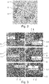
- Fig. 3
- verschiedene Gefügestrukturen nahe der Grenzschicht und in einem Abstand zu der Grenzschicht nach verschiedenen Abkühlverfahren.
- 1
- a section through a copper strip according to the invention with a coating of tin; and
- 2
- a section of a structure of the coating formed by the alloy according to the invention, in an enlarged view; and
- 3
- different microstructures near the interface and at a distance from the interface after different cooling methods.
In der
Der Basiswerkstoff 2 wird in einem Tauchverfahren beidseitig mit einer Beschichtung 3, 4 aus einer dünnen Schicht aus Zinn (Sn) beschichtet. Dieses Zinn enthält den erfindungsgemäß vorgeschlagenen Anteil an Silber. Silber ist ein Element, welches auch in kleinsten Mengen unlöslich in dem Zinn ist und damit bewusst Ausscheidungen bildet, hier die intermetallische Zwischenphase Ag3Sn. Die intermetallische Zwischenphase wird dabei beim Auftragen des Zinns in dem Tauchverfahren gebildet, wenn das Zinn auf dem Basiswerkstoff erstarrt. Ferner kann die Partikelgröße und Form auch nachträglich z.B. durch eine thermische Behandlung beeinflußt werden. Das Mengenverhältnis des Silbers zu dem Zinn ist dabei so gewählt, dass der Gewichtsanteil des Silbers in Bezug zu dem Zinn weniger als 0,5 Gewichtsprozent beträgt. Aus Kostengründen kann der Gewichtsanteil des teuren Silbers weiter auf unter 0,1 Gewichtsprozent oder sogar unter 0,05 Gewichtsprozent besonders bevorzugt bis 0,01 Gewichtsprozent reduziert werden. Auch diese sehr geringen Mengen des Silbers in der Beschichtung aus Zinn reichen aus, um eine ausreichende Zwischenphase Ag3Sn zu bilden, welche die Diffusion des Kupfers und damit die Entstehung der Cu3Sn-Phase hemmt und dadurch die Haftfestigkeit durch die vermiedenen Kirkendall-Poren erhöht.The
Als unlösliche, ausscheidungsbildende Elemente kommen ferner Antimon (Sb), Germanium (Ge), Nickel (Ni), Wismut (Bi) und Cobalt (Co) in Frage. Unter dem Begriff unlöslich und ausscheidungsbildend soll dabei die Eigenschaft verstanden werden, Ausscheidungen in der Beschichtung zu erzeugen, welche entweder durch intermetallische Zwischenphasen des Elementes zusammen mit dem Zinn oder durch Ausscheidungen der Elemente selbst gebildet sein können. Diese Ausscheidungen dienen der Hemmung der Diffusion und der dadurch bewirkten Bildung der Cu3Sn-Phase, welche ursächlich für die Bildung der Kirkendall-Poren ist, sodass durch die zugegebenen Elemente die Bildung der Kirkendall-Poren reduziert und die Haftfestigkeit erhöht werden kann.Other insoluble, precipitate-forming elements are antimony (Sb), germanium (Ge), nickel (Ni), bismuth (Bi) and cobalt (Co). The term insoluble and precipitation-forming is to be understood as meaning the property of producing precipitations in the coating, which are formed either by intermetallic intermediate phases of the element together with the tin or by precipitations of the elements can be formed themselves. These precipitates serve to inhibit diffusion and the resulting formation of the Cu3Sn phase, which is the cause of the formation of the Kirkendall pores, so that the addition of elements reduces the formation of the Kirkendall pores and increases the adhesive strength.
Das ausscheidungsbildende, unlösliche Element Silber ist hier durch ein Tauchverfahren, bevorzugt durch ein Feuerverzinnungsverfahren auf den Basiswerkstoff 2 aufgetragen worden. Es ist aber auch denkbar, das Silber und das Zinn in einem oder zwei Schritten jeweils in einem Galvanikverfahren und/oder in einer Kombination aus einem Tauchverfahren und einem Galvanikverfahren aufzutragen.The precipitation-forming, insoluble element silver has been applied to the
Dabei kann die Beschichtung 3, 4 zusätzlich in einem Reflow-Verfahren kurzzeitig wieder aufgeschmolzen werden, wodurch ungünstige Gefügeeigenschaften beseitigt werden können.In this case, the
In der
Die Ag3Sn Phase 6 bildet durch die Zugabe in dem vorgeschlagenen Anteilsbereich Körner mit einer Korngröße mit einem Flächenmittelwert von 0,01 bis 0,03 µm2 bevorzugt von 0,0140 bis 0,0180 µm2 und einem gemittelten Umfang von 0,2 bis 0,8 µm bevorzugt von 0,4 bis 0,6 µm aus, welche für den zu erreichenden Zweck der Hemmung der Ag3Sn Phase bei einer gleichzeitig möglichst geringen Menge an Silber optimal ist. Die Ag3Sn Phase 6 hemmt die Diffusion des für die Bildung der Cu3Sn Phase notwendigen Kupfers in dem an die Cu6Sn5 Phase 5 angrenzenden Bereich, so dass die Bildung der Cu3Sn Phase gehemmt wird. Dabei ist es für den zu erreichenden Zweck nicht zwangsläufig notwendig, dass die Cu6Sn5 Phase 5 vollständig durch die Ag3Sn Phase 6 umfasst ist. Es ist dabei auch nicht von Nachteil, wenn vereinzelte Körner der Cu6Sn5 Phase 5 nicht von einer Ag3Sn Phase 6 umfasst sind.The
In der
Es ist in den oberen Darstellungen erkennbar, dass sich die Ag3Sn Phase 6 bei einer schnellen Abkühlung oder Auslagerung durch Wasser in einer Partikelstruktur zwischen einem Restanteil 7 des Zinns ausbildet, wobei die Gefügestruktur nahe der Cu6Sn5 Phase 5 noch feiner ist. In der mittleren Darstellung ist die Gefügestruktur nach einer Auslagerung des Kupferbandes 1 an Luft zu erkennen, in welcher der Restanteil 7 des Zinns aufgrund der längeren Abkühlphase zu gröberen Körnern herangewachsen ist, und die Ag3Sn Phase 6 in einer feinen Nadelstruktur zwischen dem Restanteil 7 Zinn angeordnet ist. Wie in der mittleren, rechten Darstellung zu erkennen ist, ist die Nadelstruktur der Ag3Sn Phase 6 dabei nahe der Cu6Sn5 Phase 5 deutlicher ausgeprägt. In den unteren Darstellungen ist erkennbar, dass die Ag3Sn Phase 6 bei einer Auslagerung im Ofen also bei noch längeren Abkühlzeiten ebenfalls zu einer noch ausgeprägten Nadelstruktur heranwächst und durch eine ebenfalls ausgeprägteren Nadelstruktur heranwächst.It can be seen in the illustrations above that the
Anhand der Gefügestrukturen ist erkennbar, dass durch eine Auslagerung an Luft eine erwünschte nadelförmige Morphologie der Ag3Sn Phase 6 und eine ausreichende Kapselung der Cu6Sn5 Phase 5 durch die Ag3Sn Phase 6 erreicht werden kann. Da die Auslagerung an Luft überdies die kostengünstigste Variante der Auslagerung ist, ist die Auslagerung an Luft hier das bevorzugte Auslagerungsverfahren.From the microstructure it can be seen that a desired needle-shaped morphology of the
Die Grenzschicht ist hier durch eine Schicht der Cu6Sn5 Phase 5 gebildet und weist eine Dicke von 10 bis 100 µm auf. Je nach dem Anteil des Silbers kann diese Grenzschicht dicker oder auch dünner ausgebildet sein, und sie kann zusätzliche Körner der Ag3Sn Phase 6 aufweisen.The boundary layer is formed here by a layer of the
Ein weiterer positiver Effekt der Zugabe der unlöslichen, ausscheidungsbildenden Elemente ist darin zu sehen, dass die Härte der Beschichtung 3,4 nach einer thermischen Behandlung bzw. Auslagerung erhöht wird und im Idealfall damit höher als die Härte des Basiswerkstoffs 2 ist. Im Fall der Zugabe von Silber als unlösliches, ausscheidungsbildendes Element bildet sich bei der Auslagerung die Ag3Sn-Phase 6 nach dem oben beschriebenen Prinzip und führt dadurch zu einer Erhöhung der Härte.A further positive effect of the addition of the insoluble, precipitation-forming elements can be seen in the fact that the hardness of the
Dabei wird die Auslagerung bevorzugt in einem Temperaturbereich von 80 bis 150 °C über einen Zeitraum von 500 bis 1500 h Stunden vorgenommen, um den gewünschten Effekt und die Ausbildung der Gefügestruktur herbeizuführen.The aging is preferably carried out in a temperature range from 80 to 150° C. over a period of 500 to 1500 hours in order to bring about the desired effect and the formation of the microstructure.
Claims (13)
- Copper strip (1) for making electrical contacts, with- a base material (2) of copper or a copper alloy, and- a coating (3,4) of tin, wherein- the coating (3,4) of tin has a proportion of insoluble, precipitation-forming elements of 0.003 to 1.0, preferably up to 0.5, preferably up to 0.05, particularly preferably up to 0.01 weight percent, characterized in that- the insoluble, precipitation-forming element silver is present in the coating (3,4) in a proportion of 0.08 to 0.5 weight percent in the form of an Ag3Sn phase (6).
- Copper strip (1) according to claim 1, characterized in that- the insoluble, precipitation-forming elements are additionally formed by one or more of the following elements: germanium, nickel, cobalt in a proportion of 0.003 to 0.5 weight percent each.
- Copper strip (1) according to any one of claims 1 or 2, characterized in that- the Ag3Sn phase (6) is present in the coating (3,4) in particle sizes with a mean area value of 0.01 to 0.03 µm2, preferably from 0.0140 to 0.0180 µm2.
- Copper strip (1) according to any one of claims 1 to 3, characterized in that- the Ag3Sn phase (6) is present in the coating (3,4) in particle sizes with an average circumference of 0.2 to 0.8 µm, preferably 0.4 to 0.6 µm.
- Copper strip (1) according to one of claims 1 to 4, characterized in that- in the coating (3,4) and/or the base material (2) a portion of the copper is present in a Cu6Sn5 phase (5), and the Ag3Sn phase (6) is present in the area of or envelops the Cu6Sn5 phase (5).
- Copper strip (1) according to claim 5, characterized in that- the Cu6Sn5 phase (5) is arranged adjacent to an Ag3Sn phase (6) in or adjacent to a boundary layer between the base material (2) and the coating (2, 3).
- Copper strip (1) according to any one of claims 1 to 6, characterized in that- the insoluble, precipitation-forming elements are additionally formed by one or more of the following elements: antimony or bismuth in a proportion of 0.02 to 1.0 weight percent each.
- Copper strip (1) according to one of claims 1 to 7, characterized in that- the coating (3,4) has a higher hardness than the base material (2).
- Process for producing a copper strip (1) according to one of claims 1 to 8 for the manufacture of electrical contacts, with- a base material (2) of copper or a copper alloy, and- a coating (3,4) of tin,characterized in that- the coating (3, 4) of tin is applied to the base material (2) in a dipping process and/or an electroplating process with a proportion of insoluble, precipitation-forming element silver in the coating (3,4) in a proportion of 0.08 to 0.5 weight percent in the form of an Ag3Sn phase (6).
- Process according to claim 9, characterized in that- the insoluble, precipitation-forming elements are deposited on the base material (2) in a first step in the electroplating process, and- the coating (3,4) of tin is applied in a second step by the dipping process.
- Process according to one of claims 9 or 10, characterized in that- the tin coating (3,4) is applied by an electroplating process and is subjected to a reflow treatment after application.
- Process according to one of claims 9 to 11, characterized in that- the copper strip (1) is exposed to air.
- Connectors made from a copper strip (1) according to one of claims 1 to 8 or from a copper strip (1) produced by a process according to one of claims 9 to 12.
Applications Claiming Priority (2)
| Application Number | Priority Date | Filing Date | Title |
|---|---|---|---|
| DE102018208116.6A DE102018208116A1 (en) | 2018-05-23 | 2018-05-23 | Copper tape for making electrical contacts and method of making a copper tape and connectors |
| PCT/EP2019/063091 WO2019224197A1 (en) | 2018-05-23 | 2019-05-21 | Copper strip for producing electrical contacts and method for producing a copper strip and plug-in connector |
Publications (2)
| Publication Number | Publication Date |
|---|---|
| EP3797181A1 EP3797181A1 (en) | 2021-03-31 |
| EP3797181B1 true EP3797181B1 (en) | 2022-11-16 |
Family
ID=66655327
Family Applications (1)
| Application Number | Title | Priority Date | Filing Date |
|---|---|---|---|
| EP19726624.0A Active EP3797181B1 (en) | 2018-05-23 | 2019-05-21 | Copper strip for producing electrical contacts and method for producing a copper strip and plug-in connector |
Country Status (9)
| Country | Link |
|---|---|
| US (1) | US20210218171A1 (en) |
| EP (1) | EP3797181B1 (en) |
| JP (1) | JP2021524543A (en) |
| KR (1) | KR20210011951A (en) |
| CN (1) | CN112135918A (en) |
| DE (1) | DE102018208116A1 (en) |
| ES (1) | ES2935178T3 (en) |
| PL (1) | PL3797181T3 (en) |
| WO (1) | WO2019224197A1 (en) |
Families Citing this family (2)
| Publication number | Priority date | Publication date | Assignee | Title |
|---|---|---|---|---|
| DE102020006059A1 (en) | 2020-10-05 | 2022-04-07 | Wieland-Werke Aktiengesellschaft | Electrically conductive material with coating |
| CN114347586A (en) * | 2022-01-25 | 2022-04-15 | 宁波博威合金材料股份有限公司 | Copper-copper composite strip, preparation method and application |
Family Cites Families (16)
| Publication number | Priority date | Publication date | Assignee | Title |
|---|---|---|---|---|
| GB546179A (en) * | 1941-01-10 | 1942-07-01 | Victor Alexander Lowinger | Improvements in and relating to processes for the coating of metals |
| DE4005836C2 (en) * | 1990-02-23 | 1999-10-28 | Stolberger Metallwerke Gmbh | Electrical connector pair |
| DE4443461C1 (en) * | 1994-12-07 | 1996-07-04 | Wieland Werke Ag | Copper@ (alloy) composite strip or wire material used in electromechanical or electrooptical applications |
| DE19752329A1 (en) * | 1997-11-26 | 1999-05-27 | Stolberger Metallwerke Gmbh | Process for the production of a metallic composite tape |
| JPH11350190A (en) * | 1998-06-03 | 1999-12-21 | Furukawa Electric Co Ltd:The | Material for electric and electronic parts, its production, and electric and electronic parts using the same |
| DE10025106A1 (en) | 2000-05-20 | 2001-11-22 | Stolberger Metallwerke Gmbh | Electrically conductive metal tape and connectors from it |
| DE10025107A1 (en) * | 2000-05-20 | 2001-11-22 | Stolberger Metallwerke Gmbh | Electrically conductive metal band and connector |
| US6924044B2 (en) * | 2001-08-14 | 2005-08-02 | Snag, Llc | Tin-silver coatings |
| DE10139953A1 (en) | 2001-08-21 | 2003-03-27 | Stolberger Metallwerke Gmbh | Material for a metal band |
| JP4441726B2 (en) * | 2003-01-24 | 2010-03-31 | 石原薬品株式会社 | Method for producing tin or tin alloy aliphatic sulfonic acid plating bath |
| JP4740814B2 (en) * | 2006-09-29 | 2011-08-03 | Jx日鉱日石金属株式会社 | Copper alloy reflow Sn plating material with excellent whisker resistance |
| WO2008074344A1 (en) * | 2006-12-19 | 2008-06-26 | Mahle International Gmbh | Sliding bearing |
| US20080308300A1 (en) * | 2007-06-18 | 2008-12-18 | Conti Mark A | Method of manufacturing electrically conductive strips |
| JP5313773B2 (en) * | 2009-06-04 | 2013-10-09 | 三菱伸銅株式会社 | Plated copper strip and method for producing the same |
| CN101905387B (en) * | 2010-02-04 | 2012-02-15 | 哈尔滨工业大学 | Preparation method of nanometer Ag enhancing low-temperature lead-free compound soldering paste |
| CN102085604A (en) * | 2011-03-04 | 2011-06-08 | 上海交通大学 | Sn-Ag-Cu-Bi-Cr low-silver and lead-free solder |
-
2018
- 2018-05-23 DE DE102018208116.6A patent/DE102018208116A1/en not_active Ceased
-
2019
- 2019-05-21 CN CN201980033674.2A patent/CN112135918A/en not_active Withdrawn
- 2019-05-21 PL PL19726624.0T patent/PL3797181T3/en unknown
- 2019-05-21 US US17/055,016 patent/US20210218171A1/en not_active Abandoned
- 2019-05-21 ES ES19726624T patent/ES2935178T3/en active Active
- 2019-05-21 JP JP2020564679A patent/JP2021524543A/en not_active Withdrawn
- 2019-05-21 WO PCT/EP2019/063091 patent/WO2019224197A1/en unknown
- 2019-05-21 KR KR1020207035991A patent/KR20210011951A/en not_active Application Discontinuation
- 2019-05-21 EP EP19726624.0A patent/EP3797181B1/en active Active
Also Published As
| Publication number | Publication date |
|---|---|
| JP2021524543A (en) | 2021-09-13 |
| EP3797181A1 (en) | 2021-03-31 |
| US20210218171A1 (en) | 2021-07-15 |
| WO2019224197A1 (en) | 2019-11-28 |
| CN112135918A (en) | 2020-12-25 |
| PL3797181T3 (en) | 2023-03-20 |
| DE102018208116A1 (en) | 2019-11-28 |
| KR20210011951A (en) | 2021-02-02 |
| ES2935178T3 (en) | 2023-03-02 |
Similar Documents
| Publication | Publication Date | Title |
|---|---|---|
| DE60200154T2 (en) | Metallic object with multi-layer covering | |
| DE102006010760B4 (en) | Copper alloy and method of making the same | |
| DE102007047007A1 (en) | Electrical contact element and a method for producing the same | |
| EP3797181B1 (en) | Copper strip for producing electrical contacts and method for producing a copper strip and plug-in connector | |
| DE202009013202U1 (en) | Platinum jewelery alloy | |
| DE102014117410B4 (en) | Electrical contact element, press-fit pin, socket and leadframe | |
| EP1157820A1 (en) | Metal strip with high electric conductibility and connector made from it | |
| EP1421651B1 (en) | Electric contact | |
| EP1158618A2 (en) | Metal strip with high electric conductibility and connector made from it | |
| DE2448738A1 (en) | Production of a composite - by coating a metal powder with another metal applying onto a carrier with a binder and sintering | |
| WO2013087268A1 (en) | Contact element and method for the production thereof | |
| DE112016002685B4 (en) | fitting and connector | |
| DE1614668B2 (en) | Semiconductor arrangement with large-area, easily solderable contact electrodes and process for their production | |
| WO2007060078A1 (en) | Method for producing a layer on a metal element, which layer is capable of contact | |
| EP4225960A1 (en) | Electrically conducting material with coating | |
| DE102012208681A1 (en) | Tin coating, associated contact element and method for applying a tin coating | |
| EP1535730B1 (en) | Layered arrangement and composite material for electromechanical articles | |
| EP0837955B1 (en) | Copper-based sliding surface | |
| DE3434627A1 (en) | Electrical sliding contact, especially for commutation systems | |
| DE102012017520A1 (en) | A method of tin coating a metallic substrate, a method of curing a tin layer, and wire with a tin coating | |
| DE1639051C2 (en) | Method for producing an ohmic contact on a silicon semiconductor body | |
| DE10139953A1 (en) | Material for a metal band | |
| DE2603806C2 (en) | Process for the production of superconductors | |
| DE112009001549T5 (en) | Lead-free plating element and method of forming a plating layer | |
| DE102006045531B3 (en) | Method for producing a layer on a support |
Legal Events
| Date | Code | Title | Description |
|---|---|---|---|
| STAA | Information on the status of an ep patent application or granted ep patent |
Free format text: STATUS: THE INTERNATIONAL PUBLICATION HAS BEEN MADE |
|
| STAA | Information on the status of an ep patent application or granted ep patent |
Free format text: STATUS: THE INTERNATIONAL PUBLICATION HAS BEEN MADE |
|
| PUAI | Public reference made under article 153(3) epc to a published international application that has entered the european phase |
Free format text: ORIGINAL CODE: 0009012 |
|
| STAA | Information on the status of an ep patent application or granted ep patent |
Free format text: STATUS: REQUEST FOR EXAMINATION WAS MADE |
|
| 17P | Request for examination filed |
Effective date: 20201023 |
|
| AK | Designated contracting states |
Kind code of ref document: A1 Designated state(s): AL AT BE BG CH CY CZ DE DK EE ES FI FR GB GR HR HU IE IS IT LI LT LU LV MC MK MT NL NO PL PT RO RS SE SI SK SM TR |
|
| AX | Request for extension of the european patent |
Extension state: BA ME |
|
| DAV | Request for validation of the european patent (deleted) | ||
| DAX | Request for extension of the european patent (deleted) | ||
| GRAP | Despatch of communication of intention to grant a patent |
Free format text: ORIGINAL CODE: EPIDOSNIGR1 |
|
| STAA | Information on the status of an ep patent application or granted ep patent |
Free format text: STATUS: GRANT OF PATENT IS INTENDED |
|
| INTG | Intention to grant announced |
Effective date: 20220610 |
|
| GRAS | Grant fee paid |
Free format text: ORIGINAL CODE: EPIDOSNIGR3 |
|
| GRAA | (expected) grant |
Free format text: ORIGINAL CODE: 0009210 |
|
| STAA | Information on the status of an ep patent application or granted ep patent |
Free format text: STATUS: THE PATENT HAS BEEN GRANTED |
|
| AK | Designated contracting states |
Kind code of ref document: B1 Designated state(s): AL AT BE BG CH CY CZ DE DK EE ES FI FR GB GR HR HU IE IS IT LI LT LU LV MC MK MT NL NO PL PT RO RS SE SI SK SM TR |
|
| REG | Reference to a national code |
Ref country code: GB Ref legal event code: FG4D Free format text: NOT ENGLISH |
|
| REG | Reference to a national code |
Ref country code: CH Ref legal event code: EP |
|
| REG | Reference to a national code |
Ref country code: IE Ref legal event code: FG4D Free format text: LANGUAGE OF EP DOCUMENT: GERMAN |
|
| REG | Reference to a national code |
Ref country code: DE Ref legal event code: R096 Ref document number: 502019006291 Country of ref document: DE |
|
| REG | Reference to a national code |
Ref country code: AT Ref legal event code: REF Ref document number: 1531822 Country of ref document: AT Kind code of ref document: T Effective date: 20221215 |
|
| REG | Reference to a national code |
Ref country code: RO Ref legal event code: EPE |
|
| REG | Reference to a national code |
Ref country code: SE Ref legal event code: TRGR |
|
| REG | Reference to a national code |
Ref country code: SK Ref legal event code: T3 Ref document number: E 41040 Country of ref document: SK |
|
| REG | Reference to a national code |
Ref country code: ES Ref legal event code: FG2A Ref document number: 2935178 Country of ref document: ES Kind code of ref document: T3 Effective date: 20230302 |
|
| REG | Reference to a national code |
Ref country code: LT Ref legal event code: MG9D |
|
| REG | Reference to a national code |
Ref country code: NL Ref legal event code: MP Effective date: 20221116 |
|
| PG25 | Lapsed in a contracting state [announced via postgrant information from national office to epo] |
Ref country code: PT Free format text: LAPSE BECAUSE OF FAILURE TO SUBMIT A TRANSLATION OF THE DESCRIPTION OR TO PAY THE FEE WITHIN THE PRESCRIBED TIME-LIMIT Effective date: 20230316 Ref country code: NO Free format text: LAPSE BECAUSE OF FAILURE TO SUBMIT A TRANSLATION OF THE DESCRIPTION OR TO PAY THE FEE WITHIN THE PRESCRIBED TIME-LIMIT Effective date: 20230216 Ref country code: LT Free format text: LAPSE BECAUSE OF FAILURE TO SUBMIT A TRANSLATION OF THE DESCRIPTION OR TO PAY THE FEE WITHIN THE PRESCRIBED TIME-LIMIT Effective date: 20221116 Ref country code: FI Free format text: LAPSE BECAUSE OF FAILURE TO SUBMIT A TRANSLATION OF THE DESCRIPTION OR TO PAY THE FEE WITHIN THE PRESCRIBED TIME-LIMIT Effective date: 20221116 |
|
| PG25 | Lapsed in a contracting state [announced via postgrant information from national office to epo] |
Ref country code: RS Free format text: LAPSE BECAUSE OF FAILURE TO SUBMIT A TRANSLATION OF THE DESCRIPTION OR TO PAY THE FEE WITHIN THE PRESCRIBED TIME-LIMIT Effective date: 20221116 Ref country code: LV Free format text: LAPSE BECAUSE OF FAILURE TO SUBMIT A TRANSLATION OF THE DESCRIPTION OR TO PAY THE FEE WITHIN THE PRESCRIBED TIME-LIMIT Effective date: 20221116 Ref country code: IS Free format text: LAPSE BECAUSE OF FAILURE TO SUBMIT A TRANSLATION OF THE DESCRIPTION OR TO PAY THE FEE WITHIN THE PRESCRIBED TIME-LIMIT Effective date: 20230316 Ref country code: HR Free format text: LAPSE BECAUSE OF FAILURE TO SUBMIT A TRANSLATION OF THE DESCRIPTION OR TO PAY THE FEE WITHIN THE PRESCRIBED TIME-LIMIT Effective date: 20221116 Ref country code: GR Free format text: LAPSE BECAUSE OF FAILURE TO SUBMIT A TRANSLATION OF THE DESCRIPTION OR TO PAY THE FEE WITHIN THE PRESCRIBED TIME-LIMIT Effective date: 20230217 |
|
| PG25 | Lapsed in a contracting state [announced via postgrant information from national office to epo] |
Ref country code: NL Free format text: LAPSE BECAUSE OF FAILURE TO SUBMIT A TRANSLATION OF THE DESCRIPTION OR TO PAY THE FEE WITHIN THE PRESCRIBED TIME-LIMIT Effective date: 20221116 |
|
| PG25 | Lapsed in a contracting state [announced via postgrant information from national office to epo] |
Ref country code: SM Free format text: LAPSE BECAUSE OF FAILURE TO SUBMIT A TRANSLATION OF THE DESCRIPTION OR TO PAY THE FEE WITHIN THE PRESCRIBED TIME-LIMIT Effective date: 20221116 Ref country code: EE Free format text: LAPSE BECAUSE OF FAILURE TO SUBMIT A TRANSLATION OF THE DESCRIPTION OR TO PAY THE FEE WITHIN THE PRESCRIBED TIME-LIMIT Effective date: 20221116 Ref country code: DK Free format text: LAPSE BECAUSE OF FAILURE TO SUBMIT A TRANSLATION OF THE DESCRIPTION OR TO PAY THE FEE WITHIN THE PRESCRIBED TIME-LIMIT Effective date: 20221116 |
|
| PGFP | Annual fee paid to national office [announced via postgrant information from national office to epo] |
Ref country code: RO Payment date: 20230510 Year of fee payment: 5 Ref country code: IT Payment date: 20230531 Year of fee payment: 5 Ref country code: FR Payment date: 20230517 Year of fee payment: 5 Ref country code: ES Payment date: 20230621 Year of fee payment: 5 Ref country code: DE Payment date: 20230504 Year of fee payment: 5 Ref country code: CZ Payment date: 20230510 Year of fee payment: 5 |
|
| REG | Reference to a national code |
Ref country code: DE Ref legal event code: R097 Ref document number: 502019006291 Country of ref document: DE |
|
| PG25 | Lapsed in a contracting state [announced via postgrant information from national office to epo] |
Ref country code: AL Free format text: LAPSE BECAUSE OF FAILURE TO SUBMIT A TRANSLATION OF THE DESCRIPTION OR TO PAY THE FEE WITHIN THE PRESCRIBED TIME-LIMIT Effective date: 20221116 |
|
| PGFP | Annual fee paid to national office [announced via postgrant information from national office to epo] |
Ref country code: SK Payment date: 20230517 Year of fee payment: 5 Ref country code: SE Payment date: 20230522 Year of fee payment: 5 Ref country code: PL Payment date: 20230519 Year of fee payment: 5 |
|
| PLBE | No opposition filed within time limit |
Free format text: ORIGINAL CODE: 0009261 |
|
| STAA | Information on the status of an ep patent application or granted ep patent |
Free format text: STATUS: NO OPPOSITION FILED WITHIN TIME LIMIT |
|
| 26N | No opposition filed |
Effective date: 20230817 |
|
| PG25 | Lapsed in a contracting state [announced via postgrant information from national office to epo] |
Ref country code: SI Free format text: LAPSE BECAUSE OF FAILURE TO SUBMIT A TRANSLATION OF THE DESCRIPTION OR TO PAY THE FEE WITHIN THE PRESCRIBED TIME-LIMIT Effective date: 20221116 |
|
| REG | Reference to a national code |
Ref country code: CH Ref legal event code: PL |
|
| PG25 | Lapsed in a contracting state [announced via postgrant information from national office to epo] |
Ref country code: MC Free format text: LAPSE BECAUSE OF FAILURE TO SUBMIT A TRANSLATION OF THE DESCRIPTION OR TO PAY THE FEE WITHIN THE PRESCRIBED TIME-LIMIT Effective date: 20221116 |
|
| GBPC | Gb: european patent ceased through non-payment of renewal fee |
Effective date: 20230521 |
|
| REG | Reference to a national code |
Ref country code: BE Ref legal event code: MM Effective date: 20230531 |
|
| PG25 | Lapsed in a contracting state [announced via postgrant information from national office to epo] |
Ref country code: MC Free format text: LAPSE BECAUSE OF FAILURE TO SUBMIT A TRANSLATION OF THE DESCRIPTION OR TO PAY THE FEE WITHIN THE PRESCRIBED TIME-LIMIT Effective date: 20221116 Ref country code: LU Free format text: LAPSE BECAUSE OF NON-PAYMENT OF DUE FEES Effective date: 20230521 Ref country code: LI Free format text: LAPSE BECAUSE OF NON-PAYMENT OF DUE FEES Effective date: 20230531 Ref country code: CH Free format text: LAPSE BECAUSE OF NON-PAYMENT OF DUE FEES Effective date: 20230531 |
|
| REG | Reference to a national code |
Ref country code: IE Ref legal event code: MM4A |
|
| PG25 | Lapsed in a contracting state [announced via postgrant information from national office to epo] |
Ref country code: IE Free format text: LAPSE BECAUSE OF NON-PAYMENT OF DUE FEES Effective date: 20230521 |