EP3796573A1 - Mitigation of electrical-to-optical conversion impairments induced at transmitter - Google Patents
Mitigation of electrical-to-optical conversion impairments induced at transmitter Download PDFInfo
- Publication number
- EP3796573A1 EP3796573A1 EP20198885.4A EP20198885A EP3796573A1 EP 3796573 A1 EP3796573 A1 EP 3796573A1 EP 20198885 A EP20198885 A EP 20198885A EP 3796573 A1 EP3796573 A1 EP 3796573A1
- Authority
- EP
- European Patent Office
- Prior art keywords
- electrical
- optical
- transmitter
- operative
- transmitted
- Prior art date
- Legal status (The legal status is an assumption and is not a legal conclusion. Google has not performed a legal analysis and makes no representation as to the accuracy of the status listed.)
- Granted
Links
- 238000006243 chemical reaction Methods 0.000 title claims abstract description 93
- 230000006735 deficit Effects 0.000 title claims abstract description 90
- 230000000116 mitigating effect Effects 0.000 title description 2
- 230000003287 optical effect Effects 0.000 claims abstract description 136
- 238000004891 communication Methods 0.000 claims abstract description 29
- 230000010287 polarization Effects 0.000 claims description 36
- 238000012545 processing Methods 0.000 claims description 17
- 230000005540 biological transmission Effects 0.000 claims description 14
- 238000000034 method Methods 0.000 claims description 11
- 238000007493 shaping process Methods 0.000 description 11
- 238000012937 correction Methods 0.000 description 10
- 230000001427 coherent effect Effects 0.000 description 7
- 238000011084 recovery Methods 0.000 description 6
- 230000003595 spectral effect Effects 0.000 description 5
- 238000004364 calculation method Methods 0.000 description 3
- 230000000694 effects Effects 0.000 description 3
- 230000015556 catabolic process Effects 0.000 description 2
- 238000006731 degradation reaction Methods 0.000 description 2
- 238000009795 derivation Methods 0.000 description 2
- 239000006185 dispersion Substances 0.000 description 2
- 238000001914 filtration Methods 0.000 description 2
- 230000001939 inductive effect Effects 0.000 description 2
- 238000009987 spinning Methods 0.000 description 2
- 230000003044 adaptive effect Effects 0.000 description 1
- 230000032683 aging Effects 0.000 description 1
- 238000004422 calculation algorithm Methods 0.000 description 1
- 230000001934 delay Effects 0.000 description 1
- 230000001419 dependent effect Effects 0.000 description 1
- 238000010586 diagram Methods 0.000 description 1
- 230000005684 electric field Effects 0.000 description 1
- 238000012417 linear regression Methods 0.000 description 1
- 239000013307 optical fiber Substances 0.000 description 1
- 238000012360 testing method Methods 0.000 description 1
- 238000012549 training Methods 0.000 description 1
Images


Classifications
-
- H—ELECTRICITY
- H04—ELECTRIC COMMUNICATION TECHNIQUE
- H04B—TRANSMISSION
- H04B10/00—Transmission systems employing electromagnetic waves other than radio-waves, e.g. infrared, visible or ultraviolet light, or employing corpuscular radiation, e.g. quantum communication
- H04B10/40—Transceivers
-
- H—ELECTRICITY
- H04—ELECTRIC COMMUNICATION TECHNIQUE
- H04B—TRANSMISSION
- H04B10/00—Transmission systems employing electromagnetic waves other than radio-waves, e.g. infrared, visible or ultraviolet light, or employing corpuscular radiation, e.g. quantum communication
- H04B10/07—Arrangements for monitoring or testing transmission systems; Arrangements for fault measurement of transmission systems
- H04B10/075—Arrangements for monitoring or testing transmission systems; Arrangements for fault measurement of transmission systems using an in-service signal
- H04B10/079—Arrangements for monitoring or testing transmission systems; Arrangements for fault measurement of transmission systems using an in-service signal using measurements of the data signal
- H04B10/0799—Monitoring line transmitter or line receiver equipment
-
- H—ELECTRICITY
- H04—ELECTRIC COMMUNICATION TECHNIQUE
- H04B—TRANSMISSION
- H04B10/00—Transmission systems employing electromagnetic waves other than radio-waves, e.g. infrared, visible or ultraviolet light, or employing corpuscular radiation, e.g. quantum communication
- H04B10/50—Transmitters
- H04B10/516—Details of coding or modulation
- H04B10/548—Phase or frequency modulation
- H04B10/556—Digital modulation, e.g. differential phase shift keying [DPSK] or frequency shift keying [FSK]
- H04B10/5561—Digital phase modulation
-
- H—ELECTRICITY
- H04—ELECTRIC COMMUNICATION TECHNIQUE
- H04B—TRANSMISSION
- H04B10/00—Transmission systems employing electromagnetic waves other than radio-waves, e.g. infrared, visible or ultraviolet light, or employing corpuscular radiation, e.g. quantum communication
- H04B10/50—Transmitters
- H04B10/58—Compensation for non-linear transmitter output
- H04B10/588—Compensation for non-linear transmitter output in external modulation systems
-
- H—ELECTRICITY
- H04—ELECTRIC COMMUNICATION TECHNIQUE
- H04B—TRANSMISSION
- H04B10/00—Transmission systems employing electromagnetic waves other than radio-waves, e.g. infrared, visible or ultraviolet light, or employing corpuscular radiation, e.g. quantum communication
- H04B10/60—Receivers
- H04B10/61—Coherent receivers
- H04B10/616—Details of the electronic signal processing in coherent optical receivers
-
- H—ELECTRICITY
- H04—ELECTRIC COMMUNICATION TECHNIQUE
- H04L—TRANSMISSION OF DIGITAL INFORMATION, e.g. TELEGRAPHIC COMMUNICATION
- H04L1/00—Arrangements for detecting or preventing errors in the information received
- H04L1/004—Arrangements for detecting or preventing errors in the information received by using forward error control
- H04L1/0041—Arrangements at the transmitter end
- H04L1/0042—Encoding specially adapted to other signal generation operation, e.g. in order to reduce transmit distortions, jitter, or to improve signal shape
-
- H—ELECTRICITY
- H04—ELECTRIC COMMUNICATION TECHNIQUE
- H04L—TRANSMISSION OF DIGITAL INFORMATION, e.g. TELEGRAPHIC COMMUNICATION
- H04L7/00—Arrangements for synchronising receiver with transmitter
- H04L7/0075—Arrangements for synchronising receiver with transmitter with photonic or optical means
Definitions
- This document relates to the technical field of coherent optical communications and more specifically to the mitigation of electrical-to-optical conversion impairments induced at a transmitter.
- Optical communication systems with higher spectral efficiency are being developed to satisfy the ever-increasing network capacity demand.
- the system performance becomes more sensitive to the impairments from the transmitter and the receiver.
- Electrical-to-optical conversion impairments induced at the transmitter diminish achievable transceiver performance.
- a digital instruction is generated regarding one or more electrical-to-optical conversion impairments induced at the transmitter of an optical communication system.
- the digital instruction may be used by the transmitter to reduce the impairments.
- the digital instruction may be used by the receiver of the optical communication system to compensate for the impairments.
- Complex modulation schemes improve spectral efficiency by using all the parameters of a light wave for encoding information: amplitude, polarization and frequency or phase.
- the electric field envelope at any instant of a modulated light wave can be described in the complex plane as a location on an I/Q diagram.
- I is the in-phase or real part
- Q is the quadrature or imaginary part.
- a symbol (also called a "constellation point") is defined by its (I,Q) values, or in polar coordinates by amplitude E and phase ⁇ .
- An optical signal is composed of a modulated optical carrier.
- the optical carrier comprises two orthogonal polarized components, for example an X-polarized component and a Y-polarized component.
- Two dimensions (in-phase and quadrature) of each polarized component have been modulated according to a respective two of the analog electrical signals, for example, an analog in-phase electrical signal X I and an analog quadrature electrical signal X Q for the X-polarized component, and an analog in-phase electrical signal Y I and an analog quadrature electrical signal Y Q for the Y-polarized component.
- FIG. 1 illustrates the principles of electrical-to-optical conversion at a transmitter.
- a continuous wave (CW) optical carrier 100 is generated by a laser 102 and modulated by a Mach-Zehnder interferometer 104.
- the CW optical carrier is split into two beams. One beam follows a path where the beam is modulated by a Mach-Zehnder interferometer 106 that is driven by an analog in-phase electrical signal D I (for example, X I or Y I ) to produce an in-phase modulated carrier 108, represented mathematically as D I ⁇ cos[ ⁇ (t- ⁇ )].
- D I analog in-phase electrical signal
- the other beam follows a path where the beam is modulated by a Mach-Zehnder interferometer 110 that is driven by an analog quadrature electrical signal D Q (for example, X Q or Y Q ), and then phase shifted by a phase shifter 112, to produce a quadrature modulated carrier 114, represented mathematically as g ⁇ D Q ⁇ sin[ ⁇ t+ ⁇ ].
- D Q for example, X Q or Y Q
- a phase shifter 112 phase shifted by a phase shifter 112
- the two modulated beams are then combined into a single beam 116.
- timing skew In non-ideal electrical-to-optical conversion, there is a non-zero time delay (also known as "timing skew") between the in-phase modulated carrier 108 and the quadrature modulated carrier 114, the phase difference between the in-phase modulated carrier 108 and the quadrature modulated carrier 114 is not exactly 90 degrees ⁇ 2 radians , and there is a power imbalance between the in-phase modulated carrier 108 and the quadrature modulated carrier 114.
- the timing skew is illustrated by an IQ timing skew factor ⁇
- the phase difference is illustrated by a quadrature angle error ⁇
- the power imbalance is illustrated by a gain factor g.
- E/O electrical-to-optical
- the primary causes of E/O conversion impairments induced at the transmitter include differential delays and amplitudes as well as non-orthogonality in the I and Q fields delivered to the modulator output. These are typically minimized once at start of life by factory calibration. Some are, in addition, corrected over life using control methods local to the transmitter. Implemented impairments over life remain due to any local control error as well as error and drift in calibration which may be caused by aging of transmitter components, thermal effects, and humidity effects. Rates of change of measurable impairments are on the order of seconds to minutes to even longer durations.
- IQ power imbalance is handled by dead reckoning calibration at the start of life, and local control solutions at the transmitter during service are awkward as they require dedicated O/E conversion hardware. If the IQ power imbalance were estimated or measured at a conventional receiver, an attempt to correct the IQ power imbalance at the conventional receiver would not fully recover the induced performance degradation.
- a local control solution at the transmitter for correction of IQ timing skew and quadrature angle error requires dithers and loop SNR considerations such that temporary misalignment produced by a practical dither constitutes a non-negligible noise.
- the equivalent noise of a given IQ timing skew is pro-rated to the transceiver baud and, to affect cost reduction, baud generally increases with successive transceiver product generations.
- the use of dithers as a means of E/O converter control becomes more problematic as the transceiver product advances.
- This disclosure proposes generating a digital instruction regarding the one or more E/O conversion impairments induced at the transmitter.
- the digital instruction is used by the transmitter to reduce the E/O conversion impairments.
- the digital instruction is used by the receiver to compensate for the E/O conversion impairments.
- FIG. 2 illustrates an example optical communication system 200.
- a transmitter 202 is operative to produce a transmitted optical signal 204 which is transmitted over a transmission medium 206 to a receiver 208 that receives a received optical signal 210.
- the transmission medium 206 comprises optical fibers, optical amplifiers, optical filters, optical switches, and optical add-drop multiplexers.
- the optical communication system 200 occurs between satellites through near-vacuum.
- the receiver 208 is operative to derive received symbols 212 from the received optical signal 210.
- the transmitted optical signal 204 conveys data. In some implementations, the receiver 208 makes decisions to reconstruct the data.
- the receiver 208 makes decisions regarding the received symbols 212 to derive encoded bits, and then decodes the encoded bits with error correction to reconstruct the data.
- the transmission medium 206 is bi-directional.
- the receiver 208 is operative to transmit information to the transmitter 202, and the transmitter 202 is operative to receive the information from the receiver 208.
- the transmitter 202 induces one or more E/O conversion impairments in the transmitted optical signal 204.
- An estimator 214 is operative to generate from the received symbols 212 a digital instruction 216 regarding the one or more E/O conversion impairments induced at the transmitter 202. Details regarding the operation of the estimator 214 are described below.
- the estimator 214 is located at the receiver 208 and provides the digital instruction 216 to the receiver 208, and the receiver 208 is operative to compensate for the one or more E/O conversion impairments according to the digital instruction 216.
- This implementation may use a prior art transmitter such as described below with respect to FIG. 3 or any other suitable transmitter.
- An example receiver that is operative to compensate for the one or more E/O conversion impairments is described below with respect to FIG. 6 .
- the estimator 214 is located at the receiver 208 and uses the receiver 208 to provide the digital instruction 216 to the transmitter 202 over a channel (not shown), and the transmitter 202 is operative to reduce the one or more E/O conversion impairments according to the digital instruction 216.
- An example transmitter that is operative to reduce the one or more E/O conversion impairments is described below with respect to FIG. 4 .
- This implementation may use a receiver such as described below with respect to FIG. 5 or a receiver such as described below with respect to FIG. 6 or any other suitable receiver.
- This implementation may use a receiver such as described below with respect to FIG. 9 that corrects distortions resulting from the one or more E/O conversion impairments, so that the transmitter 202 is operative to reduce the part of the one or more E/O conversion impairments that are not compensated at the receiver.
- the estimator 214 is located at the receiver 208 and provides the digital instruction 216 to the receiver 208 and uses the receiver 208 to provide the digital instruction 216 to the transmitter 202 over a channel (not shown).
- the transmitter 202 is operative to reduce partially the one or more E/O conversion impairments according to the digital instruction 216
- the receiver 208 is operative to compensate partially for the one or more E/O conversion impairments according to the digital instruction 216.
- An example receiver that is operative to compensate for the one or more E/O conversion impairments is described below with respect to FIG. 6 .
- An example transmitter that is operative to reduce the one or more E/O conversion impairments is described below with respect to FIG. 4 .
- the estimator 214 is located at the transmitter 202, and the receiver 208 is operative to provide the received symbols 212 to the transmitter 202 over a channel (not shown) for use by the estimator.
- the transmitter 202 is operative to reduce the one or more E/O conversion impairments according to the digital instruction 216.
- An example transmitter that is operative to reduce the one or more E/O conversion impairments is described below with respect to FIG. 4 .
- This implementation may use a receiver such as described below with respect to FIG. 5 or a receiver such as described below with respect to FIG. 6 or any other suitable receiver. In a variant of this implementation (not illustrated in FIG.
- the functionality of the estimator 214 is split between a first portion that is located at the receiver 208 and a second portion that is located at the transmitter 202, with the first portion using the receiver 208 to provide to the second portion information derived from the received symbols 212 and from which the digital instruction 216 can be derived.
- the received optical signal 210 has the same E/O conversion impairments that were induced by the transmitter 202 in the transmitted optical signal 204. Stated differently, it is not believed that the transmission medium 206 induces in the received optical signal 210 any further IQ timing skew, quadrature angle error or IQ power imbalance beyond the E/O conversion impairments that are already present in the transmitted optical signal 204.
- FIG. 3 illustrates an example transmitter 300.
- the transmitter 300 is an example of the transmitter 202.
- the transmitter 300 comprises a forward error correction (FEC) encoder 304 coupled to a modulation encoder 306 coupled to a digital signal processor (DSP) 308 coupled to digital-to-analog converters 310 coupled to radio frequency (RF) drivers 312 coupled to E/O converters 314.
- the DSP 308 comprises one or more digital pulse-shaping filters 316.
- the FEC encoder 304 applies an FEC algorithm to incoming digital data 318 to encode the digital data 318 into coded bits 320.
- the incoming digital data 318 may be comprised to two separate data streams that are encoded separately into two separate streams of coded bits.
- the modulation encoder 306 maps the coded bits 320 to symbols of a constellation comprising a first polarization (for example, an X polarization) and a second polarization (for example, a Y polarization) that is orthogonal to the first polarization.
- the DSP 308 receives as input the symbol instructions 324 for the X-polarization and performs spectral shaping and optionally additional processing, thus producing a digital in-phase X I signal 326 and a digital quadrature X Q signal 328.
- the DSP 308 receives as input the symbol instructions 330 for the Y-polarization and performs spectral shaping and optionally additional processing, thus producing a digital in-phase Y I signal 332 and a digital quadrature Y Q signal 334.
- the digital-to-analog converters 310 convert the digital signals 326, 328, 332 and 334 into respective analog electrical signals 336, 338, 342 and 344.
- the symbols 324, 330 are referred to in this disclosure as "transmitted symbols”.
- a first of the E/O converters 314 converts the analog in-phase X I electrical signal 336 and the analog quadrature X Q electrical signal 338 into a first polarized optical signal 346, in keeping with the principles of electrical-to-optical conversion described above with respect to FIG. 1 .
- the first E/O converter 314 induces one or more first electrical-to-optical impairments in the first polarized optical signal 346.
- a second of the E/O converters 314 converts the analog in-phase Y I electrical signal 342 and the analog quadrature Y Q electrical signal 344 into a first polarized optical signal 348, in keeping with the principles of electrical-to-optical conversion described above with respect to FIG. 1 .
- the second E/O converter 314 induces one or more second electrical-to-optical impairments in the second polarized optical signal 348.
- the first polarized optical signal 346 and the second polarized optical signal 348 are combined into a single transmitted optical signal 350.
- the transmitted optical signal 350 is an example of the transmitted optical signal 204.
- FIG. 4 illustrates another example transmitter 400.
- the transmitter 400 is another example of the transmitter 202.
- the transmitter 400 differs from the transmitter 300, at least in that the transmitter 400 comprises E/O converters 414 (instead of the E/O converters 314) and a control block 416 to control components of the transmitter 400 to reduce the E/O conversion impairments according to digital instructions 216.
- the components controlled by the control block 416 include the E/O converters 414 and, optionally, the one or more digital pulse-shaping filters 316 of the DSP 308.
- the control block 416 may be a generic processor or a dedicated processor or any suitable combination of hardware, firmware and software.
- a receiver (not shown) that is co-located with the transmitter 400 receives backward transmissions from the receiver 208.
- the co-located receiver may receive an optical version of the digital instructions 216 over a channel (not shown) and provide the digital instructions 216 to the control block 416.
- the control block 416 may reduce the power imbalance by adjusting the relative power of the in-phase portion and the quadrature portion prior to their combination into a single polarized optical signal.
- the control block 416 may control the power of the analog in-phase electrical signal D I that drives the Mach-Zehnder interferometer 106, for example, by adjusting the gain of a variable gain amplifier 120 (see FIG. 1 ).
- control block 416 may control the power of the analog quadrature electrical signal D Q that drives the Mach-Zehnder interferometer 110, for example, by adjusting the gain of a variable gain amplifier 122 (see FIG. 1 ).
- control block 416 may scale the taps of the one or more digital pulse-shaping filters 316 to separately affect the analog in-phase electrical signal D I that drives the Mach-Zehnder interferometer 106 and the analog quadrature electrical signal D Q that drives the Mach-Zehnder interferometer 110.
- the control block 416 may reduce the power imbalance via a combination of two or three of the techniques described above.
- the control block 416 may reduce the timing skew through adjustment of the taps of the one or more digital pulse-shaping filters 316 in the DSP 308 to apply a time shift to the digital signal.
- the control block 416 may reduce the timing skew through use of a phase shifter (not shown) acting on the analog electrical signal or acting on the optical signal.
- control block 416 may reduce the timing skew partially through adjustment of the one or more digital pulse-shaping filters 316 in the DSP 308 and partially through use of a phase shifter (not shown) acting on the analog electrical signal or acting on the optical signal. Fine adjustment of the timing skew may be accomplished more successfully in the digital domain, and coarse adjustment of the timing skew may be accomplished more successfully in the analog domain.
- the control block 416 may reduce the quadrature angle error by adjusting a relative phase of the in-phase portion of the polarized optical signal and the quadrature portion of the polarized optical signal. For example, the control block 416 may adjust the phase shifter 112 of that E/O converter 414. Alternatively or additionally, the control block 416 may adjust the taps on the one or more digital pulse-shaping filters 316 to reduce the quadrature angle error. Alternatively or additionally, the control block 416 may control the one or more digital pulse-shaping filters 316 to perform a filtering technique such as described in US Patent No. 7769305 to reduce the quadrature angle error.
- FIG. 5 illustrates an example receiver 500.
- the receiver 500 is an example of the receiver 208.
- the receiver 500 comprises a local oscillator 502 coupled to a coherent optical receiver 504 coupled to RF drivers 506 coupled to analog-to-digital converters 508 coupled to a DSP 510 coupled to a carrier recovery module 512 coupled to a modulation decoder 514 coupled to a FEC decoder 516.
- a description of the receiver 500 in operation follows.
- a continuous wave (CW) signal 518 produced by the local oscillator 502 and a received optical signal 520 are input to the coherent optical receiver 504.
- the coherent optical receiver 504 performs optical-to-electrical (O/E) conversion for a first polarization (for example, an X polarization) and for a second polarization (for example, a Y polarization) that is orthogonal to the first polarization.
- the coherent optical receiver 504 produces an analog in-phase X I ' electrical signal 522, an analog quadrature X Q ' electrical signal 524, an analog in-phase Y I ' electrical signal 526, and an analog quadrature Y Q ' electrical signal 528.
- the RF drivers 506 amplify the analog electrical signals 522, 524, 526, 528 and the analog-to-digital converters 508 sample the amplified signals to produce digital in-phase X I ' signal 532, digital quadrature X Q ' signal 534, digital in-phase Y I ' signal 536, and digital quadrature Y Q ' signal 538.
- the coherent optical receiver 504 induces O/E conversion impairments that are similar to the E/O conversion impairments induced at the transmitter. There is a frequency offset between the local oscillator 502 and continuous wave optical carrier generated by the laser at the transmitter. This frequency offset causes a phase drift (spinning the signal in the complex plane) that is corrected by the carrier recovery module 512. As a result of the spinning, the receiver O/E conversion impairments are eliminated in the estimator 214 when the estimated values are averaged over many received symbols.
- the DSP 510 receives as input the digital signals 532, 534, 536 and 538 and performs digital filtering, clock recovery, polarization recovery, and other processing.
- the DSP 510 may perform chromatic dispersion compensation.
- the DSP 510 may include an adaptive multiple-in multiple-out (MIMO) filter.
- MIMO adaptive multiple-in multiple-out
- the signal processing performed by the DSP 510 substantially effects an inverse of the channel over which the optical signal 520 was received.
- the carrier recovery module 512 processes the output of the DSP 510 and derives received symbols 540, 542 for the two orthogonal polarizations.
- the received symbols 540, 542 (or a subset of the received symbols 540, 542) are examples of the received symbols 212 that are provided to the estimator 214. This is illustrated in FIG. 5 by arrows 541 and 543.
- the modulation decoder 514 makes decisions regarding the received symbols 540, 542 to derive encoded bits 544, and then the FEC decoder 516 decodes the encoded bits 544 with error correction to reconstruct the data 546.
- FIG. 6 illustrates another example receiver 600.
- the receiver 600 is another example of the receiver 208.
- the receiver 600 differs from the receiver 500, at least in that the receiver 600 comprises a DSP 616 to compensate for the E/O conversion impairments according to digital instructions 216.
- the DSP 616 receives as input the same received symbols 540, 542 that are provided to the estimator 214 and based on which the estimator 214 generates the digital instructions 216. For example, the DSP 616 may adjust the decision boundaries that determine whether a received constellation point is one transmitted symbol or a different transmitted symbol, in order to compensate for the E/O conversion impairments.
- the estimator 214 can be implemented in hardware, firmware, software, or a combination thereof. Implementations of the estimator 214 may involve use of physical, tangible computer-readable media that store instructions which, when executed by a processor, result in the calculations described below.
- a [ k ] is the Fourier Transform (FT) of a [ n ];
- B [ k ] is the FT of b [ n ];
- C [ k ] is the FT of c [ n ];
- D [ k ] is the FT of d [ n ].
- the estimator 214 uses a cross-correlation of real (in-phase) and imaginary (quadrature) parts of the received symbols 212 to generate the digital instruction 216 regarding the quadrature angle error induced at the transmitter 202.
- the quadrature angle error ⁇ can be estimated as follows: ⁇ ⁇ arcsin 2 ⁇ E c n ⁇ d n E c n 2 + d n 2 where E is the expected value, that is, a summation over time.
- E [ c [ n ] ⁇ d [ n ]] is a measure of the cross-correlation of the real and imaginary parts of the received symbols 212.
- the expression E [ c [ n ] 2 + d [ n ] 2 ] is a measure of power in the received symbols.
- the digital instruction 216 generated by the estimator 214 may convey the quadrature angle error by including a present value of the quadrature angle error, or a direction of change to achieve orthogonality, or some other digital representation of a control error signal. Appendix A provides a derivation of Equation 2.
- the estimator 214 uses a phase difference in the frequency domain between i) real parts of the received symbols 212 and the transmitted symbols and ii) imaginary parts of the received symbols 212 and the transmitted symbols to generate the digital instruction 216 regarding the timing skew induced at the transmitter 202.
- the received symbols 212 may correspond to known transmitted symbols, for example, training symbols used to calibrate or test the system 200.
- the estimator 214 uses the received symbols 212 and the known transmitted symbols to generate the digital instruction 216 regarding the timing skew induced at the transmitter 202.
- the estimator 214 derives transmitted symbols from the received symbols 212 by performing a decision, which may include error correction, on the received symbols 212, and the estimator 214 then uses the received symbols 212 and the derived transmitted symbols to generate the digital instruction 216 regarding the timing skew induced at the transmitter 202.
- FIG. 7 illustrates an example estimator 700.
- the estimator 700 is an example of the estimator 214.
- a transmitted symbol module 702 determines transmitted symbols 704.
- the transmitted symbol module 702 may derive the transmitted symbols 704 from the received symbols 212 by performing a hard decision on the received symbols 212.
- the transmitted symbol module 702 may determine the transmitted symbols 704 to be known transmitted symbols that are stored in the receiver 208 and provided by the receiver 208 to the estimator 700.
- An E/O conversion impairment estimation module 706 receives as input the received symbols 212 that are derived at the receiver 208 and the transmitted symbols 704 that are determined by the transmitted symbol module 704.
- the E/O conversion impairment estimation module 702 performs the calculations described above on its input and outputs the digital instructions 216.
- FIG. 8 illustrates another example estimator 800.
- the estimator 800 is another example of the estimator 214.
- the estimator 800 differs from the estimator 700, at least in that the estimator 800 comprises a processing component 802 and a processing component 804.
- the transmitter 202 performs additional processing that mixes the in-phase and quadrature portions of the transmitted symbols prior to the electrical-to-optical conversion at the transmitter 202.
- additional processing may include chromatic dispersion pre-compensation, and Jones rotation to mitigate the performance degradation caused by polarization dependent loss.
- the DSP 308 in the transmitter 300 or in the transmitter 400 may perform such additional processing.
- the estimator 800 is appropriate for these implementations.
- the processing component 802 applies the same additional processing to the received symbols 212 to generate processed received symbols 806.
- the processing component 804 applies the same additional processing to the transmitted symbols 704 to generate processed transmitted symbols 808.
- the E/O conversion impairment estimation module 706 receives as input the processed received symbols 806 and the processed transmitted symbols 808.
- the E/O conversion impairment estimation module 706 performs the calculations described above on its input and outputs the digital instructions 216.
- FIG. 9 illustrates another example receiver 900.
- the receiver 900 is another example of the receiver 208.
- the receiver 900 differs from the receiver 500, at least in that the receiver 900 comprises a DSP 916 that corrects IQ distortions resulting from the E/O conversion impairments.
- the power imbalance between an in-phase portion of the transmitted optical signal and a quadrature portion of the transmitted optical signal results in different signal-to-noise ratios (SNR) on the I and Q tributaries at the receiver 900, despite the correction of the IQ distortions by the DSP 916.
- SNR signal-to-noise ratios
- the quadrature angle error at the transmitter 202 results in noise correlation between the I and Q tributaries at the receiver 900, despite the correction of the IQ distortions by the DSP 916.
- Received symbols 940, 942 are output from the DSP 916 and are provided to the estimator 214, as illustrated in FIG. 9 by arrows 941 and 943.
- the estimator 214 generates the digital instruction 216 based on the received symbols 940, 942. In this situation, the estimator 214 estimates the power imbalance using the variance difference between real (in-phase) and imaginary (quadrature) parts of the noise. In this situation, the estimator 214 estimates the quadrature angle error using the covariance between real (in-phase) and imaginary (quadrature) parts of the noise.
- the digital instruction 216 is sent to the transmitter 202, and the transmitter 202 reduces the one or more electrical-to-optical conversion impairments according to the digital instruction 216.
Landscapes
- Physics & Mathematics (AREA)
- Engineering & Computer Science (AREA)
- Computer Networks & Wireless Communication (AREA)
- Signal Processing (AREA)
- Electromagnetism (AREA)
- Nonlinear Science (AREA)
- Optics & Photonics (AREA)
- Optical Communication System (AREA)
Abstract
Description
- This document relates to the technical field of coherent optical communications and more specifically to the mitigation of electrical-to-optical conversion impairments induced at a transmitter.
- Optical communication systems with higher spectral efficiency are being developed to satisfy the ever-increasing network capacity demand. As the cardinality of the signal modulation increases, the system performance becomes more sensitive to the impairments from the transmitter and the receiver. Electrical-to-optical conversion impairments induced at the transmitter diminish achievable transceiver performance.
- A digital instruction is generated regarding one or more electrical-to-optical conversion impairments induced at the transmitter of an optical communication system. The digital instruction may be used by the transmitter to reduce the impairments. Alternatively, or additionally, the digital instruction may be used by the receiver of the optical communication system to compensate for the impairments.
-
-
FIG. 1 illustrates principles of electrical-to-optical conversion at an example transmitter; -
FIG. 2 illustrates an example optical communication system; -
FIG. 3 (PRIOR ART) illustrates an example transmitter; -
FIG. 4 illustrates another example transmitter; -
FIG. 5 illustrates an example receiver; -
FIG. 6 illustrates another example receiver; -
FIG. 7 illustrates an example estimator; -
FIG. 8 illustrates another example estimator; -
FIG. 9 illustrates yet another example receiver; -
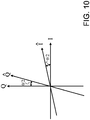
FIG. 10 illustrates a complex plane; and - Appendix A is a derivation of the estimated quadrature angle error.
- Complex modulation schemes improve spectral efficiency by using all the parameters of a light wave for encoding information: amplitude, polarization and frequency or phase. For a given polarization, the electric field envelope at any instant of a modulated light wave can be described in the complex plane as a location on an I/Q diagram. I is the in-phase or real part, and Q is the quadrature or imaginary part. A symbol (also called a "constellation point") is defined by its (I,Q) values, or in polar coordinates by amplitude E and phase ϕ.
- An optical signal is composed of a modulated optical carrier. The optical carrier comprises two orthogonal polarized components, for example an X-polarized component and a Y-polarized component. Two dimensions (in-phase and quadrature) of each polarized component have been modulated according to a respective two of the analog electrical signals, for example, an analog in-phase electrical signal XI and an analog quadrature electrical signal XQ for the X-polarized component, and an analog in-phase electrical signal YI and an analog quadrature electrical signal YQ for the Y-polarized component.
-
FIG. 1 illustrates the principles of electrical-to-optical conversion at a transmitter. A continuous wave (CW)optical carrier 100 is generated by alaser 102 and modulated by a Mach-Zehnderinterferometer 104. The CW optical carrier is split into two beams. One beam follows a path where the beam is modulated by a Mach-Zehnder interferometer 106 that is driven by an analog in-phase electrical signal DI (for example, XI or YI) to produce an in-phase modulatedcarrier 108, represented mathematically as DI·cos[ω(t-τ)]. The other beam follows a path where the beam is modulated by a Mach-Zehnderinterferometer 110 that is driven by an analog quadrature electrical signal DQ (for example, XQ or YQ), and then phase shifted by aphase shifter 112, to produce a quadrature modulatedcarrier 114, represented mathematically as g·DQ·sin[ωt+θ]. The two modulated beams are then combined into asingle beam 116. - In non-ideal electrical-to-optical conversion, there is a non-zero time delay (also known as "timing skew") between the in-phase modulated
carrier 108 and the quadrature modulatedcarrier 114, the phase difference between the in-phase modulatedcarrier 108 and the quadrature modulatedcarrier 114 is not exactly 90 degrees
carrier 108 and the quadrature modulatedcarrier 114. InFIG. 1 , the timing skew is illustrated by an IQ timing skew factor τ, the phase difference is illustrated by a quadrature angle error θ, and the power imbalance is illustrated by a gain factor g. Collectively, the IQ timing skew, quadrature angle error and IQ power imbalance are referred to in this disclosure as electrical-to-optical (E/O) conversion impairments induced at the transmitter. - The primary causes of E/O conversion impairments induced at the transmitter include differential delays and amplitudes as well as non-orthogonality in the I and Q fields delivered to the modulator output. These are typically minimized once at start of life by factory calibration. Some are, in addition, corrected over life using control methods local to the transmitter. Implemented impairments over life remain due to any local control error as well as error and drift in calibration which may be caused by aging of transmitter components, thermal effects, and humidity effects. Rates of change of measurable impairments are on the order of seconds to minutes to even longer durations.
- In conventional transmitters, IQ power imbalance is handled by dead reckoning calibration at the start of life, and local control solutions at the transmitter during service are awkward as they require dedicated O/E conversion hardware. If the IQ power imbalance were estimated or measured at a conventional receiver, an attempt to correct the IQ power imbalance at the conventional receiver would not fully recover the induced performance degradation.
- In conventional transmitters, a local control solution at the transmitter for correction of IQ timing skew and quadrature angle error requires dithers and loop SNR considerations such that temporary misalignment produced by a practical dither constitutes a non-negligible noise. The equivalent noise of a given IQ timing skew is pro-rated to the transceiver baud and, to affect cost reduction, baud generally increases with successive transceiver product generations. Thus, the use of dithers as a means of E/O converter control becomes more problematic as the transceiver product advances.
- This disclosure proposes generating a digital instruction regarding the one or more E/O conversion impairments induced at the transmitter. In some implementations, the digital instruction is used by the transmitter to reduce the E/O conversion impairments. In other implementations, the digital instruction is used by the receiver to compensate for the E/O conversion impairments.
-
FIG. 2 illustrates an exampleoptical communication system 200. Atransmitter 202 is operative to produce a transmittedoptical signal 204 which is transmitted over atransmission medium 206 to areceiver 208 that receives a receivedoptical signal 210. In some implementations, thetransmission medium 206 comprises optical fibers, optical amplifiers, optical filters, optical switches, and optical add-drop multiplexers. In other implementations, theoptical communication system 200 occurs between satellites through near-vacuum. Thereceiver 208 is operative to derive receivedsymbols 212 from the receivedoptical signal 210. The transmittedoptical signal 204 conveys data. In some implementations, thereceiver 208 makes decisions to reconstruct the data. In other implementations, thereceiver 208 makes decisions regarding the receivedsymbols 212 to derive encoded bits, and then decodes the encoded bits with error correction to reconstruct the data. Thetransmission medium 206 is bi-directional. Thereceiver 208 is operative to transmit information to thetransmitter 202, and thetransmitter 202 is operative to receive the information from thereceiver 208. - In use, the
transmitter 202 induces one or more E/O conversion impairments in the transmittedoptical signal 204. Anestimator 214 is operative to generate from the received symbols 212 adigital instruction 216 regarding the one or more E/O conversion impairments induced at thetransmitter 202. Details regarding the operation of theestimator 214 are described below. - In one implementation, the
estimator 214 is located at thereceiver 208 and provides thedigital instruction 216 to thereceiver 208, and thereceiver 208 is operative to compensate for the one or more E/O conversion impairments according to thedigital instruction 216. This implementation may use a prior art transmitter such as described below with respect toFIG. 3 or any other suitable transmitter. An example receiver that is operative to compensate for the one or more E/O conversion impairments is described below with respect toFIG. 6 . - In another implementation, the
estimator 214 is located at thereceiver 208 and uses thereceiver 208 to provide thedigital instruction 216 to thetransmitter 202 over a channel (not shown), and thetransmitter 202 is operative to reduce the one or more E/O conversion impairments according to thedigital instruction 216. An example transmitter that is operative to reduce the one or more E/O conversion impairments is described below with respect toFIG. 4 . This implementation may use a receiver such as described below with respect toFIG. 5 or a receiver such as described below with respect toFIG. 6 or any other suitable receiver. This implementation may use a receiver such as described below with respect toFIG. 9 that corrects distortions resulting from the one or more E/O conversion impairments, so that thetransmitter 202 is operative to reduce the part of the one or more E/O conversion impairments that are not compensated at the receiver. - In a further implementation, the
estimator 214 is located at thereceiver 208 and provides thedigital instruction 216 to thereceiver 208 and uses thereceiver 208 to provide thedigital instruction 216 to thetransmitter 202 over a channel (not shown). In this implementation, thetransmitter 202 is operative to reduce partially the one or more E/O conversion impairments according to thedigital instruction 216, and thereceiver 208 is operative to compensate partially for the one or more E/O conversion impairments according to thedigital instruction 216. An example receiver that is operative to compensate for the one or more E/O conversion impairments is described below with respect toFIG. 6 . An example transmitter that is operative to reduce the one or more E/O conversion impairments is described below with respect toFIG. 4 . - In yet another implementation, the
estimator 214 is located at thetransmitter 202, and thereceiver 208 is operative to provide the receivedsymbols 212 to thetransmitter 202 over a channel (not shown) for use by the estimator. In this implementation, thetransmitter 202 is operative to reduce the one or more E/O conversion impairments according to thedigital instruction 216. An example transmitter that is operative to reduce the one or more E/O conversion impairments is described below with respect toFIG. 4 . This implementation may use a receiver such as described below with respect toFIG. 5 or a receiver such as described below with respect toFIG. 6 or any other suitable receiver. In a variant of this implementation (not illustrated inFIG. 2 ), the functionality of theestimator 214 is split between a first portion that is located at thereceiver 208 and a second portion that is located at thetransmitter 202, with the first portion using thereceiver 208 to provide to the second portion information derived from the receivedsymbols 212 and from which thedigital instruction 216 can be derived. - It is expected that the received
optical signal 210 has the same E/O conversion impairments that were induced by thetransmitter 202 in the transmittedoptical signal 204. Stated differently, it is not believed that thetransmission medium 206 induces in the receivedoptical signal 210 any further IQ timing skew, quadrature angle error or IQ power imbalance beyond the E/O conversion impairments that are already present in the transmittedoptical signal 204. -
FIG. 3 (PRIOR ART) illustrates anexample transmitter 300. Thetransmitter 300 is an example of thetransmitter 202. Thetransmitter 300 comprises a forward error correction (FEC)encoder 304 coupled to a modulation encoder 306 coupled to a digital signal processor (DSP) 308 coupled to digital-to-analog converters 310 coupled to radio frequency (RF)drivers 312 coupled to E/O converters 314. TheDSP 308 comprises one or more digital pulse-shapingfilters 316. A description of thetransmitter 300 in operation follows. - The
FEC encoder 304 applies an FEC algorithm to incomingdigital data 318 to encode thedigital data 318 into codedbits 320. The incomingdigital data 318 may be comprised to two separate data streams that are encoded separately into two separate streams of coded bits. The modulation encoder 306 maps the codedbits 320 to symbols of a constellation comprising a first polarization (for example, an X polarization) and a second polarization (for example, a Y polarization) that is orthogonal to the first polarization. TheDSP 308 receives as input thesymbol instructions 324 for the X-polarization and performs spectral shaping and optionally additional processing, thus producing a digital in-phase XI signal 326 and a digital quadrature XQ signal 328. TheDSP 308 receives as input thesymbol instructions 330 for the Y-polarization and performs spectral shaping and optionally additional processing, thus producing a digital in-phase YI signal 332 and a digital quadrature YQ signal 334. The digital-to-analog converters 310 convert thedigital signals electrical signals symbols - A first of the E/
O converters 314 converts the analog in-phase XIelectrical signal 336 and the analog quadrature XQelectrical signal 338 into a first polarizedoptical signal 346, in keeping with the principles of electrical-to-optical conversion described above with respect toFIG. 1 . The first E/O converter 314 induces one or more first electrical-to-optical impairments in the first polarizedoptical signal 346. - A second of the E/
O converters 314 converts the analog in-phase YIelectrical signal 342 and the analog quadrature YQelectrical signal 344 into a first polarizedoptical signal 348, in keeping with the principles of electrical-to-optical conversion described above with respect toFIG. 1 . The second E/O converter 314 induces one or more second electrical-to-optical impairments in the second polarizedoptical signal 348. - The first polarized
optical signal 346 and the second polarizedoptical signal 348 are combined into a single transmittedoptical signal 350. The transmittedoptical signal 350 is an example of the transmittedoptical signal 204. -
FIG. 4 illustrates anotherexample transmitter 400. Thetransmitter 400 is another example of thetransmitter 202. Thetransmitter 400 differs from thetransmitter 300, at least in that thetransmitter 400 comprises E/O converters 414 (instead of the E/O converters 314) and acontrol block 416 to control components of thetransmitter 400 to reduce the E/O conversion impairments according todigital instructions 216. The components controlled by thecontrol block 416 include the E/O converters 414 and, optionally, the one or more digital pulse-shapingfilters 316 of theDSP 308. Thecontrol block 416 may be a generic processor or a dedicated processor or any suitable combination of hardware, firmware and software. A receiver (not shown) that is co-located with thetransmitter 400 receives backward transmissions from thereceiver 208. For example, the co-located receiver may receive an optical version of thedigital instructions 216 over a channel (not shown) and provide thedigital instructions 216 to thecontrol block 416. - In response to a
digital instruction 216 that identifies a power imbalance induced by one of the E/O converters 414 between an in-phase portion of the polarized optical signal and a quadrature portion of the polarized optical signal, thecontrol block 416 may reduce the power imbalance by adjusting the relative power of the in-phase portion and the quadrature portion prior to their combination into a single polarized optical signal. For example, thecontrol block 416 may control the power of the analog in-phase electrical signal DI that drives the Mach-Zehnder interferometer 106, for example, by adjusting the gain of a variable gain amplifier 120 (seeFIG. 1 ). Alternatively, thecontrol block 416 may control the power of the analog quadrature electrical signal DQ that drives the Mach-Zehnder interferometer 110, for example, by adjusting the gain of a variable gain amplifier 122 (seeFIG. 1 ). In another alternative, thecontrol block 416 may scale the taps of the one or more digital pulse-shapingfilters 316 to separately affect the analog in-phase electrical signal DI that drives the Mach-Zehnder interferometer 106 and the analog quadrature electrical signal DQ that drives the Mach-Zehnder interferometer 110. In a further alternative, thecontrol block 416 may reduce the power imbalance via a combination of two or three of the techniques described above. - In response to a
digital instruction 216 that identifies a timing skew induced by one of the E/O converters 414 between an in-phase portion of the polarized optical signal and a quadrature portion of the polarized optical signal, thecontrol block 416 may reduce the timing skew through adjustment of the taps of the one or more digital pulse-shapingfilters 316 in theDSP 308 to apply a time shift to the digital signal. Alternatively, thecontrol block 416 may reduce the timing skew through use of a phase shifter (not shown) acting on the analog electrical signal or acting on the optical signal. In a further alternative, thecontrol block 416 may reduce the timing skew partially through adjustment of the one or more digital pulse-shapingfilters 316 in theDSP 308 and partially through use of a phase shifter (not shown) acting on the analog electrical signal or acting on the optical signal. Fine adjustment of the timing skew may be accomplished more successfully in the digital domain, and coarse adjustment of the timing skew may be accomplished more successfully in the analog domain. - In response to a
digital instruction 216 that identifies a quadrature angle error induced by one of the E/O converters 414, thecontrol block 416 may reduce the quadrature angle error by adjusting a relative phase of the in-phase portion of the polarized optical signal and the quadrature portion of the polarized optical signal. For example, thecontrol block 416 may adjust thephase shifter 112 of that E/O converter 414. Alternatively or additionally, thecontrol block 416 may adjust the taps on the one or more digital pulse-shapingfilters 316 to reduce the quadrature angle error. Alternatively or additionally, thecontrol block 416 may control the one or more digital pulse-shapingfilters 316 to perform a filtering technique such as described inUS Patent No. 7769305 to reduce the quadrature angle error. -
FIG. 5 illustrates anexample receiver 500. Thereceiver 500 is an example of thereceiver 208. Thereceiver 500 comprises alocal oscillator 502 coupled to a coherentoptical receiver 504 coupled to RF drivers 506 coupled to analog-to-digital converters 508 coupled to aDSP 510 coupled to acarrier recovery module 512 coupled to amodulation decoder 514 coupled to aFEC decoder 516. A description of thereceiver 500 in operation follows. - A continuous wave (CW) signal 518 produced by the
local oscillator 502 and a receivedoptical signal 520 are input to the coherentoptical receiver 504. The coherentoptical receiver 504 performs optical-to-electrical (O/E) conversion for a first polarization (for example, an X polarization) and for a second polarization (for example, a Y polarization) that is orthogonal to the first polarization. The coherentoptical receiver 504 produces an analog in-phase XI'electrical signal 522, an analog quadrature XQ'electrical signal 524, an analog in-phase YI'electrical signal 526, and an analog quadrature YQ'electrical signal 528. The RF drivers 506 amplify the analogelectrical signals digital converters 508 sample the amplified signals to produce digital in-phase XI'signal 532, digital quadrature XQ'signal 534, digital in-phase YI'signal 536, and digital quadrature YQ'signal 538. - The coherent
optical receiver 504 induces O/E conversion impairments that are similar to the E/O conversion impairments induced at the transmitter. There is a frequency offset between thelocal oscillator 502 and continuous wave optical carrier generated by the laser at the transmitter. This frequency offset causes a phase drift (spinning the signal in the complex plane) that is corrected by thecarrier recovery module 512. As a result of the spinning, the receiver O/E conversion impairments are eliminated in theestimator 214 when the estimated values are averaged over many received symbols. - The
DSP 510 receives as input thedigital signals DSP 510 may perform chromatic dispersion compensation. TheDSP 510 may include an adaptive multiple-in multiple-out (MIMO) filter. Typically, the signal processing performed by theDSP 510 substantially effects an inverse of the channel over which theoptical signal 520 was received. - The
carrier recovery module 512 processes the output of theDSP 510 and derives receivedsymbols symbols 540, 542 (or a subset of the receivedsymbols 540, 542) are examples of the receivedsymbols 212 that are provided to theestimator 214. This is illustrated inFIG. 5 byarrows - The
modulation decoder 514 makes decisions regarding the receivedsymbols bits 544, and then theFEC decoder 516 decodes the encodedbits 544 with error correction to reconstruct thedata 546. -
FIG. 6 illustrates anotherexample receiver 600. Thereceiver 600 is another example of thereceiver 208. Thereceiver 600 differs from thereceiver 500, at least in that thereceiver 600 comprises aDSP 616 to compensate for the E/O conversion impairments according todigital instructions 216. TheDSP 616 receives as input the same receivedsymbols estimator 214 and based on which theestimator 214 generates thedigital instructions 216. For example, theDSP 616 may adjust the decision boundaries that determine whether a received constellation point is one transmitted symbol or a different transmitted symbol, in order to compensate for the E/O conversion impairments. - The
estimator 214 can be implemented in hardware, firmware, software, or a combination thereof. Implementations of theestimator 214 may involve use of physical, tangible computer-readable media that store instructions which, when executed by a processor, result in the calculations described below. - The following nomenclature is used in the discussion of the operation of the
estimator 214. The transmitted symbols for one of the polarizations are x[n]=a[n]+jb[n] and the receivedsymbols 212 for that one of the polarization are s[n]=c[n]+jd[n]. In the frequency domain, A[k] is the Fourier Transform (FT) of a[n]; B[k] is the FT of b[n]; C[k] is the FT of c[n]; and D[k] is the FT of d[n]. - The
estimator 214 uses a power difference between real (in-phase) and imaginary (quadrature) parts of the receivedsymbols 212 to generate thedigital instruction 216 regarding the IQ power imbalance induced at thetransmitter 202. For example, assuming that the in-phase and quadrature parts of the transmitted symbols have the same power (prior to pulse shaping, digital-to-analog conversion, and electrical-to-optical conversion at the transmitter 202), then the power imbalance, in decibels, can be estimated as follows:
digital instruction 216 generated by theestimator 214 may convey the estimated power imbalance by including the power imbalance value, or an identification of the highest or lowest power phase, or some other digital representation of one of this information. - The
estimator 214 uses a cross-correlation of real (in-phase) and imaginary (quadrature) parts of the receivedsymbols 212 to generate thedigital instruction 216 regarding the quadrature angle error induced at thetransmitter 202. For example, the quadrature angle error θ can be estimated as follows:
symbols 212. The expression E[c[n]2+d[n]2] is a measure of power in the received symbols. Thedigital instruction 216 generated by theestimator 214 may convey the quadrature angle error by including a present value of the quadrature angle error, or a direction of change to achieve orthogonality, or some other digital representation of a control error signal. Appendix A provides a derivation of Equation 2. - The
estimator 214 uses a phase difference in the frequency domain between i) real parts of the receivedsymbols 212 and the transmitted symbols and ii) imaginary parts of the receivedsymbols 212 and the transmitted symbols to generate thedigital instruction 216 regarding the timing skew induced at thetransmitter 202. The receivedsymbols 212 may correspond to known transmitted symbols, for example, training symbols used to calibrate or test thesystem 200. In cases where the receivedsymbols 212 correspond to known transmitted symbols (which are stored at thereceiver 208 and provided by thereceiver 208 to the estimator 214), theestimator 214 uses the receivedsymbols 212 and the known transmitted symbols to generate thedigital instruction 216 regarding the timing skew induced at thetransmitter 202. In cases where the receivedsymbols 212 do not correspond to known transmitted symbols, theestimator 214 derives transmitted symbols from the receivedsymbols 212 by performing a decision, which may include error correction, on the receivedsymbols 212, and theestimator 214 then uses the receivedsymbols 212 and the derived transmitted symbols to generate thedigital instruction 216 regarding the timing skew induced at thetransmitter 202. - For example, the timing skew τ can be estimated based on a least-square linear regression as follows:


θ andk indicates an arithmetic mean. - PI [k] is defined as the product of the frequency-domain signal of the real part of the received symbol and the conjugate of the frequency-domain signal of the real part of the transmitted symbol, averaged across FT blocks to suppress noise interference:

- PQ [k] is defined as the product of the frequency-domain signal of the imaginary part of the received symbol and the conjugate of the frequency-domain signal of the imaginary part of the transmitted symbol, averaged across FT blocks to suppress noise interference:

-
FIG. 7 illustrates anexample estimator 700. Theestimator 700 is an example of theestimator 214. A transmittedsymbol module 702 determines transmittedsymbols 704. The transmittedsymbol module 702 may derive the transmittedsymbols 704 from the receivedsymbols 212 by performing a hard decision on the receivedsymbols 212. Alternatively, the transmittedsymbol module 702 may determine the transmittedsymbols 704 to be known transmitted symbols that are stored in thereceiver 208 and provided by thereceiver 208 to theestimator 700. - An E/O conversion
impairment estimation module 706 receives as input the receivedsymbols 212 that are derived at thereceiver 208 and the transmittedsymbols 704 that are determined by the transmittedsymbol module 704. The E/O conversionimpairment estimation module 702 performs the calculations described above on its input and outputs thedigital instructions 216. -
FIG. 8 illustrates anotherexample estimator 800. Theestimator 800 is another example of theestimator 214. Theestimator 800 differs from theestimator 700, at least in that theestimator 800 comprises aprocessing component 802 and aprocessing component 804. - In some implementations, the
transmitter 202 performs additional processing that mixes the in-phase and quadrature portions of the transmitted symbols prior to the electrical-to-optical conversion at thetransmitter 202. Such additional processing may include chromatic dispersion pre-compensation, and Jones rotation to mitigate the performance degradation caused by polarization dependent loss. For example, theDSP 308 in thetransmitter 300 or in thetransmitter 400 may perform such additional processing. Theestimator 800 is appropriate for these implementations. Theprocessing component 802 applies the same additional processing to the receivedsymbols 212 to generate processed receivedsymbols 806. Theprocessing component 804 applies the same additional processing to the transmittedsymbols 704 to generate processed transmittedsymbols 808. The E/O conversionimpairment estimation module 706 receives as input the processed receivedsymbols 806 and the processed transmittedsymbols 808. The E/O conversionimpairment estimation module 706 performs the calculations described above on its input and outputs thedigital instructions 216. -
FIG. 9 illustrates anotherexample receiver 900. Thereceiver 900 is another example of thereceiver 208. Thereceiver 900 differs from thereceiver 500, at least in that thereceiver 900 comprises aDSP 916 that corrects IQ distortions resulting from the E/O conversion impairments. The power imbalance between an in-phase portion of the transmitted optical signal and a quadrature portion of the transmitted optical signal results in different signal-to-noise ratios (SNR) on the I and Q tributaries at thereceiver 900, despite the correction of the IQ distortions by theDSP 916. The quadrature angle error at thetransmitter 202 results in noise correlation between the I and Q tributaries at thereceiver 900, despite the correction of the IQ distortions by theDSP 916.Received symbols DSP 916 and are provided to theestimator 214, as illustrated inFIG. 9 byarrows estimator 214 generates thedigital instruction 216 based on the receivedsymbols estimator 214 estimates the power imbalance using the variance difference between real (in-phase) and imaginary (quadrature) parts of the noise. In this situation, theestimator 214 estimates the quadrature angle error using the covariance between real (in-phase) and imaginary (quadrature) parts of the noise. Thedigital instruction 216 is sent to thetransmitter 202, and thetransmitter 202 reduces the one or more electrical-to-optical conversion impairments according to thedigital instruction 216. - The scope of the invention is defined by the claims.
- The following clauses set out features of the invention which may or may not presently be claimed in this application but which may form the basis for future amendment or a divisional application.
- 1. An optical communication system (200) comprising: a transmitter (202,300,400) operative to produce and transmit a transmitted optical signal (204,350) over a transmission medium (206), the transmitter operative to induce one or more electrical-to-optical conversion impairments in the transmitted optical signal; a receiver (208,500,600,900) operative to receive a received optical signal (210,520) over the transmission medium and to derive received symbols (212,540,542,940,942) from the received optical signal; and an estimator (214,700,800) operative to generate from the received symbols a digital instruction (216) regarding the one or more electrical-to-optical conversion impairments induced at the transmitter.
- 2. The optical communication system recited in clause 1, wherein the estimator is located at the receiver (600), and the receiver (600) is operative to compensate for the one or more electrical-to-optical conversion impairments according to the digital instruction.
- 3. The optical communication system recited in clause 1, wherein the transmitter (400) is operative to reduce the one or more electrical-to-optical conversion impairments according to the digital instruction.
- 4. The optical communication system recited in clause 3, wherein the estimator is located at the transmitter (400), and the receiver (500,600) is operative to provide the received symbols to the transmitter (400) over a channel for use by the estimator; or wherein the estimator is located at the receiver (208,500,600,900), and the estimator is operative to use the receiver to provide the digital instruction to the transmitter (400) over a channel.
- 5. The optical communication system recited in clause 3, wherein the one or more electrical-to-optical conversion impairments comprise quadrature angle error, and the estimator is operative to use a covariance of real and imaginary parts of noise after compensation at the receiver (900) of the one or more electrical-to-optical conversion impairments to generate the digital instruction regarding the quadrature angle error; and/or the one or more electrical-to-optical conversion impairments comprise a power imbalance between an in-phase portion of the transmitted optical signal and a quadrature portion of the transmitted optical signal, and the estimator is operative to use a power difference between the real and imaginary parts of the noise after compensation at the receiver (900) of the one or more electrical-to-optical conversion impairments to generate the digital instruction regarding the power imbalance.
- 6. The optical communication system recited in any one of clauses 1 to 4, wherein the one or more electrical-to-optical conversion impairments comprise quadrature angle error, and the estimator is operative to use a cross-correlation of real and imaginary parts of the received symbols to generate the digital instruction regarding the quadrature angle error; and/or the one or more electrical-to-optical conversion impairments comprise a power imbalance between an in-phase portion of the transmitted optical signal and a quadrature portion of the transmitted optical signal, and the estimator is operative to use a power difference between real and imaginary parts of the received symbols to generate the digital instruction regarding the power imbalance.
- 7. The optical communication system recited in any one of clauses 1 to 6, wherein the one or more electrical-to-optical conversion impairments comprise a timing skew between an in-phase portion of the transmitted optical signal and a quadrature portion of the transmitted optical signal, and the estimator is operative to use a phase difference in the frequency domain between i) real parts of the received symbols and transmitted symbols and ii) imaginary parts of the received symbols and the transmitted symbols to generate the digital instruction regarding the timing skew.
- 8. The optical communication system recited in clause 7, wherein the transmitted symbols are known transmitted symbols, or the estimator (700,800) is operative to derive the transmitted symbols from the received symbols.
- 9. The optical communication system recited in any one of clauses 1 to 8, wherein the transmitter comprises a digital signal processor, DSP, (308) that is operative to perform processing that results in a mixing of in-phase and quadrature portions of transmitted symbols prior to electrical-to-optical conversion, and the estimator (800) is operative to process the received symbols in a manner equivalent to the processing by the DSP and to generate the digital instruction from the processed received symbols.
- 10. The optical communication system recited in any one of clauses 1 to 9, wherein the transmitted optical signal comprises two orthogonally-polarized optical signals, the receiver is operative to derive first received symbols for a first polarization state and second received symbols for a second polarization state, and the estimator is operative to generate a first digital instruction regarding one or more electrical-to-optical conversion impairments for the first polarization state from the first received symbols and to generate a second digital instruction regarding one or more electrical-to-optical conversion impairments for the second polarization state.
- 11. An optical transmitter (202,400) comprising: a forward error correction, FEC, encoder (302) to encode data (318) into coded bits (320); a modulation encoder (304) to map the coded bits to symbols (324,330) of a constellation for a first polarization and for a second polarization that is orthogonal to the first polarization; a digital signal processor (308) to perform spectral shaping of the symbols, thus producing digital in-phase and quadrature signals (326,328,332,334) for each of the polarizations; digital-to-analog converters (310) to convert the digital in-phase and quadrature signals to respective analog in-phase and quadrature electrical signals (336,338,342,344); a first electrical-to-optical, E/O, converter (414) to convert the analog in-phase and quadrature electrical signals for the first polarization to a first polarized optical signal (346) having the first polarization, the first E/O converter inducing one or more first electrical-to-optical conversion impairments in the first polarized optical signal; a second E/O converter (414) to convert the analog electrical signals for the second polarization to a second polarized optical signal (348) having the second polarization, the second E/O converter inducing one or more second electrical-to-optical conversion impairments in the second polarized optical signal; and a control block (416) to control at least one component of the transmitter to reduce the one or more first electrical-to-optical conversion impairments according to a first digital instruction (216) and to control at least one component of the transmitter to reduce the one or more second electrical-to-optical conversion impairments according to a second digital instruction (216), wherein the first polarized optical signal and the second polarized optical signal are combined into a single transmitted optical signal (350).
- 12. The optical transmitter recited in clause 11, wherein the one or more first electrical-to-optical conversion impairments comprise a timing skew between an in-phase portion of the first polarized optical signal and a quadrature portion of the first polarized optical signal, and the transmitter is operative to reduce the timing skew through use of a phase shifter (112) and/or through adjustment of the taps of a digital filter (316) in the digital signal processor.
- 13. The optical transmitter recited in clause 11 or clause 12, wherein the one or more first electrical-to-optical conversion impairments comprise quadrature angle error, and the transmitter is operative to reduce the quadrature angle error by adjusting a relative phase of an in-phase portion of the first polarized optical signal and a quadrature portion of the first polarized optical signal.
- 14. The optical transmitter recited in any one of clause 11 to 13, wherein the one or more first electrical-to-optical conversion impairments comprise a power imbalance between an in-phase portion of the first polarized optical signal and a quadrature portion of the first polarized optical signal, and the transmitter is operative to reduce the power imbalance by adjusting a relative power of the in-phase portion and the quadrature portion prior to the combination of the in-phase portion and the quadrature portion into the first polarized optical signal.
- 15. An optical receiver (208,600) comprising: a local oscillator (502) to generate a continuous wave signal (518); a coherent optical receiver (504) to receive a transmitted optical signal (210,520) over a transmission medium from an optical transmitter (202,300,400) and to generate analog in-phase electrical signals (522,526) and analog quadrature electrical signals (524,528) from the transmitted optical signal and the continuous wave signal; analog-to-digital converters (508) to convert the analog in-phase and quadrature electrical signals to respective digital in-phase and quadrature signals (532,534,536,538); a first digital signal processor (510) to process the digital in-phase and quadrature signals; a carrier recovery module (512) to derive received symbols (212,540,542) from the processed digital in-phase and quadrature signals; a second digital signal processor (616) to process the received symbols to compensate, according to a digital instruction (216), for one or more electrical-to-optical conversion impairments induced at the optical transmitter; a modulation decoder (514) to make decisions regarding the processed received symbols to derive encoded bits (544); and a forward error correction decoder (516) to decode the encoded bits with error correction to reconstruct data (546).


Claims (11)
- An optical communication system (200) comprising:a transmitter (202,300,400) operative to produce and transmit a transmitted optical signal (204,350) over a transmission medium (206), the transmitter operative to induce one or more electrical-to-optical conversion impairments in the transmitted optical signal;a receiver (208,500,600,900) operative to receive a received optical signal (210,520) over the transmission medium and to derive received symbols from the received optical signal; andan estimator (214,700,800) operative to generate from the received symbols a digital instruction (216) regarding the one or more electrical-to-optical conversion impairments induced at the transmitter,wherein the one or more electrical-to-optical conversion impairments comprise a timing skew between an in-phase portion of the transmitted optical signal and a quadrature portion of the transmitted optical signal, and the estimator is operative to use a phase difference in the frequency domain between i) real parts of the received symbols and transmitted symbols and ii) imaginary parts of the received symbols and the transmitted symbols to generate the digital instruction regarding the timing skew.
- The optical communication system recited in claim 1, wherein the transmitted symbols are known transmitted symbols.
- The optical communication system recited in claim 1, wherein the estimator is operative to derive the transmitted symbols from the received symbols.
- An optical communication system (200) comprising:a transmitter (202,300,400) operative to produce and transmit a transmitted optical signal (204,350) over a transmission medium (206), the transmitter operative to induce one or more electrical-to-optical conversion impairments in the transmitted optical signal;a receiver (208,500,600,900) operative to receive a received optical signal (210,520) over the transmission medium and to derive received symbols (212,540,542,940,942) from the received optical signal; andan estimator (214,700,800) operative to generate from the received symbols a digital instruction (216) regarding the one or more electrical-to-optical conversion impairments induced at the transmitter,wherein the one or more electrical-to-optical conversion impairments comprise a power imbalance between an in-phase portion of the transmitted optical signal and a quadrature portion of the transmitted optical signal, and the estimator is operative to use a power difference between real and imaginary parts of the received symbols to generate the digital instruction regarding the power imbalance.
- An optical communication system (200) comprising:a transmitter (202,300,400) operative to produce and transmit a transmitted optical signal (204,350) over a transmission medium (206), the transmitter operative to induce one or more electrical-to-optical conversion impairments in the transmitted optical signal;a receiver (208,500,600,900) operative to receive a received optical signal (210,520) over the transmission medium and to derive received symbols (212,540,542,940,942) from the received optical signal; andan estimator (800) operative to generate from the received symbols a digital instruction (216) regarding the one or more electrical-to-optical conversion impairments induced at the transmitter,wherein the transmitter comprises a digital signal processor, DSP, (308) that is operative to perform processing that results in a mixing of in-phase and quadrature portions of transmitted symbols prior to electrical-to-optical conversion, and the estimator (800) is operative to process the received symbols in a manner equivalent to the processing by the DSP and to generate the digital instruction from the processed received symbols.
- The optical communication system recited in any one of claims 1 to 5, wherein the receiver is operative to compensate for the one or more electrical-to-optical conversion impairments according to the digital instruction.
- The optical communication system recited in any one of claims 1 to 5, wherein the transmitter is operative to reduce the one or more electrical-to-optical conversion impairments according to the digital instruction.
- The optical communication system recited in any one of claims 1 to 5, wherein the transmitter is operative to reduce partially the one or more electrical-to-optical conversion impairments according to the digital instruction and the receiver is operative to compensate partially for the one or more electrical-to-optical conversion impairments according to the digital instruction.
- A method comprising:generating, from first received symbols for a first polarization state, a first digital instruction (216) regarding one or more electrical-to-optical conversion impairments for the first polarization state in a transmitted optical signal (204,350), the transmitted optical signal comprising two orthogonally-polarized optical signals, the one or more electrical-to-optical conversion impairments for the first polarization state induced at a transmitter (202,300,400) of an optical communication system;generating, from second received symbols for a second polarization state, a second digital instruction (216) regarding one or more electrical-to-optical conversion impairments for the second polarization state in the transmitted optical signal, the one or more electrical-to-optical conversion impairments for the second polarization state induced at the transmitter; andcompensating for the one or more electrical-to-optical conversion impairments according to the first digital instruction and the second digital instruction,wherein the first received symbols and the second received symbols were derived by a receiver (208,500,600,900) of the optical communication system from a received optical signal (210,520) corresponding to the transmitted optical signal, andwherein compensating for the one or more electrical-to-optical conversion impairments according to the first digital instruction and the second digital instruction is performed by the transmitter.
- The method recited in claim 9, wherein the one or more electrical-to-optical conversion impairments comprise a power imbalance between an in-phase portion of the transmitted optical signal and a quadrature portion of the transmitted optical signal, and generating the first digital instruction and the second digital instruction regarding the power imbalance comprises using a power difference between real and imaginary parts of noise after compensation at the receiver of the one or more electrical-to-optical conversion impairments.
- The method recited in claim 9, wherein the one or more electrical-to-optical conversion impairments comprise quadrature angle error, and generating the first digital instruction and the second digital instruction regarding the quadrature angle error comprises using a covariance of real and imaginary parts of noise after compensation at the receiver of the one or more electrical-to-optical conversion impairments.
Applications Claiming Priority (2)
| Application Number | Priority Date | Filing Date | Title |
|---|---|---|---|
| US15/046,763 US10014947B2 (en) | 2016-02-18 | 2016-02-18 | Mitigation of electrical-to-optical conversion impairments induced at transmitter |
| EP17152918.3A EP3208952B1 (en) | 2016-02-18 | 2017-01-24 | Mitigation of electrical-to-optical conversion impairments induced at transmitter |
Related Parent Applications (1)
| Application Number | Title | Priority Date | Filing Date |
|---|---|---|---|
| EP17152918.3A Division EP3208952B1 (en) | 2016-02-18 | 2017-01-24 | Mitigation of electrical-to-optical conversion impairments induced at transmitter |
Publications (2)
| Publication Number | Publication Date |
|---|---|
| EP3796573A1 true EP3796573A1 (en) | 2021-03-24 |
| EP3796573B1 EP3796573B1 (en) | 2024-03-06 |
Family
ID=57890717
Family Applications (2)
| Application Number | Title | Priority Date | Filing Date |
|---|---|---|---|
| EP17152918.3A Active EP3208952B1 (en) | 2016-02-18 | 2017-01-24 | Mitigation of electrical-to-optical conversion impairments induced at transmitter |
| EP20198885.4A Active EP3796573B1 (en) | 2016-02-18 | 2017-01-24 | Mitigation of electrical-to-optical conversion impairments induced at transmitter |
Family Applications Before (1)
| Application Number | Title | Priority Date | Filing Date |
|---|---|---|---|
| EP17152918.3A Active EP3208952B1 (en) | 2016-02-18 | 2017-01-24 | Mitigation of electrical-to-optical conversion impairments induced at transmitter |
Country Status (2)
| Country | Link |
|---|---|
| US (2) | US10014947B2 (en) |
| EP (2) | EP3208952B1 (en) |
Families Citing this family (12)
| Publication number | Priority date | Publication date | Assignee | Title |
|---|---|---|---|---|
| US9882653B2 (en) * | 2015-04-10 | 2018-01-30 | Arista Networks, Inc. | System and method of de-skewing electrical signals |
| US10014947B2 (en) * | 2016-02-18 | 2018-07-03 | Ciena Corporation | Mitigation of electrical-to-optical conversion impairments induced at transmitter |
| US10498456B2 (en) * | 2016-12-19 | 2019-12-03 | Cable Television Laboratories, Inc | System and methods for cable fiber node splitting using coherent optics |
| EP3637324A1 (en) * | 2018-10-08 | 2020-04-15 | Nokia Solutions and Networks Oy | Geometric constellation shaping for optical data transport |
| US10880019B1 (en) * | 2018-12-20 | 2020-12-29 | Acacia Communications, Inc | Impairment generation |
| US11228366B2 (en) * | 2019-02-28 | 2022-01-18 | Ntt Electronics Corporation | Optical transmission characteristics estimation method, optical transmission characteristics estimation system, and optical transmission characteristics compensation system |
| US11002632B2 (en) * | 2019-06-28 | 2021-05-11 | Viavi Solutions Inc. | Measuring polarization extinction ratio (PER) using a reference master test jumper (MTJ) |
| WO2021086578A1 (en) | 2019-10-31 | 2021-05-06 | Ciena Corporation | Asymmetric direct detection of optical signals |
| US20200174514A1 (en) * | 2020-02-03 | 2020-06-04 | Intel Corporation | Optical signal skew compensation |
| JP2022108790A (en) * | 2021-01-14 | 2022-07-27 | 富士通株式会社 | Transmission device and method of setting transmission parameters |
| US11558120B1 (en) * | 2021-09-30 | 2023-01-17 | United States Of America As Represented By The Administrator Of Nasa | Method for deskewing FPGA transmitter channels directly driving an optical QPSK modulator |
| US11581951B1 (en) * | 2022-01-31 | 2023-02-14 | Huawei Technologies Co., Ltd. | Apparatuses and methods of far-end transmitter skew monitoring in digital subcarrier multiplexing systems |
Citations (4)
| Publication number | Priority date | Publication date | Assignee | Title |
|---|---|---|---|---|
| US20100067902A1 (en) * | 2008-09-16 | 2010-03-18 | Nortel Networks Limited | Optical transmitter error reduction using receiver feedback |
| US7769305B1 (en) | 2005-10-21 | 2010-08-03 | Nortel Networks Limited | High-speed digital signal processing in a coherent optical receiver |
| US20120057863A1 (en) * | 2010-09-07 | 2012-03-08 | Alcatel-Lucent Usa Inc. | Frequency-dependent i/q-signal imbalance correction for coherent optical transceivers |
| EP2930865A1 (en) * | 2014-04-07 | 2015-10-14 | Alcatel Lucent | Transmitter quadrature imbalance compensation at a coherent optical receiver |
Family Cites Families (7)
| Publication number | Priority date | Publication date | Assignee | Title |
|---|---|---|---|---|
| US7457538B2 (en) | 2002-05-15 | 2008-11-25 | Nortel Networks Limited | Digital performance monitoring for an optical communications system |
| US7787778B2 (en) | 2004-12-10 | 2010-08-31 | Ciena Corporation | Control system for a polar optical transmitter |
| US7676161B2 (en) | 2004-12-10 | 2010-03-09 | Nortel Networks Limited | Modulation E-field based control of a non-linear transmitter |
| US8249467B2 (en) | 2010-03-11 | 2012-08-21 | Ciena Corporation | Self test of a dual polarization transmitter |
| US8565621B2 (en) * | 2011-03-01 | 2013-10-22 | Opnext Subsystems, Inc. | Quadrature time skew detection for coherent optical signals |
| US9184834B1 (en) * | 2012-12-28 | 2015-11-10 | Juniper Networks, Inc. | Method and apparatus for detection and correction of time skew in an optical transmitter |
| US10014947B2 (en) * | 2016-02-18 | 2018-07-03 | Ciena Corporation | Mitigation of electrical-to-optical conversion impairments induced at transmitter |
-
2016
- 2016-02-18 US US15/046,763 patent/US10014947B2/en active Active
-
2017
- 2017-01-24 EP EP17152918.3A patent/EP3208952B1/en active Active
- 2017-01-24 EP EP20198885.4A patent/EP3796573B1/en active Active
-
2018
- 2018-07-02 US US16/024,980 patent/US10608746B2/en active Active
Patent Citations (4)
| Publication number | Priority date | Publication date | Assignee | Title |
|---|---|---|---|---|
| US7769305B1 (en) | 2005-10-21 | 2010-08-03 | Nortel Networks Limited | High-speed digital signal processing in a coherent optical receiver |
| US20100067902A1 (en) * | 2008-09-16 | 2010-03-18 | Nortel Networks Limited | Optical transmitter error reduction using receiver feedback |
| US20120057863A1 (en) * | 2010-09-07 | 2012-03-08 | Alcatel-Lucent Usa Inc. | Frequency-dependent i/q-signal imbalance correction for coherent optical transceivers |
| EP2930865A1 (en) * | 2014-04-07 | 2015-10-14 | Alcatel Lucent | Transmitter quadrature imbalance compensation at a coherent optical receiver |
Also Published As
| Publication number | Publication date |
|---|---|
| US20170244489A1 (en) | 2017-08-24 |
| US20180331762A1 (en) | 2018-11-15 |
| EP3208952B1 (en) | 2020-09-30 |
| US10014947B2 (en) | 2018-07-03 |
| EP3796573B1 (en) | 2024-03-06 |
| US10608746B2 (en) | 2020-03-31 |
| EP3208952A1 (en) | 2017-08-23 |
Similar Documents
| Publication | Publication Date | Title |
|---|---|---|
| US10608746B2 (en) | Mitigation of electrical-to-optical conversion impairments induced at transmitter | |
| US9614621B2 (en) | Signal generating circuit, optical signal transmitting apparatus, signal receiving circuit, method for establishing optical signal synchronization, and optical signal synchronization system | |
| EP3553973B1 (en) | Optical transmission characteristic estimation method, optical transmission characteristic compensation method, optical transmission characteristic estimation system and optical transmission characteristic compensation system | |
| EP2097997B1 (en) | Adaptive polarization tracking and equalization in coherent optical receivers | |
| US8655191B2 (en) | Symbol timing recovery in polarization division multiplexed coherent optical transmission system | |
| US8744275B2 (en) | System, method, and apparatus for high-sensitivity optical detection | |
| US9954615B2 (en) | Optical up/down conversion-type optical phase conjugate pair signal transmission/reception circuit | |
| EP2169867B1 (en) | A decision directed algorithm for adjusting a polarization demultiplexer in a coherent detection optical receiver | |
| US9667347B2 (en) | Optical transmitter, optical receiver, method of compensating non-linear distortion, and communication apparatus | |
| JP5438856B1 (en) | Optical transmission / reception system, transmitter, receiver, and optical transmission / reception method | |
| US8433205B2 (en) | Crosstalk-free high-dimensional constellations for dual-polarized nonlinear fiber-optic communications | |
| US20120224862A1 (en) | System, Method, and Apparatus for High-Sensitivity Optical Detection | |
| EP2273700B1 (en) | Dual-polarization optical bursts for reception by a coherent burst mode receiver with fast adaption | |
| EP3051723B1 (en) | Polarisation mode dispersion (pmd) tolerant optical signaling | |
| Peng et al. | Compensation for I/Q imbalances and bias deviation of the Mach–Zehnder modulators in direct-detected optical OFDM systems | |
| JP6025918B1 (en) | Optical receiver and coherent optical communication system | |
| EP4354745A1 (en) | Signal processing method, signal processing device, and communication system | |
| Zhu et al. | Training-aided PDM 64-QAM transmission with enhanced fiber nonlinearity tolerance | |
| JP5969661B1 (en) | Optical transmitter and optical transmission / reception system |
Legal Events
| Date | Code | Title | Description |
|---|---|---|---|
| PUAI | Public reference made under article 153(3) epc to a published international application that has entered the european phase |
Free format text: ORIGINAL CODE: 0009012 |
|
| STAA | Information on the status of an ep patent application or granted ep patent |
Free format text: STATUS: THE APPLICATION HAS BEEN PUBLISHED |
|
| AC | Divisional application: reference to earlier application |
Ref document number: 3208952 Country of ref document: EP Kind code of ref document: P |
|
| AK | Designated contracting states |
Kind code of ref document: A1 Designated state(s): AL AT BE BG CH CY CZ DE DK EE ES FI FR GB GR HR HU IE IS IT LI LT LU LV MC MK MT NL NO PL PT RO RS SE SI SK SM TR |
|
| RIN1 | Information on inventor provided before grant (corrected) |
Inventor name: O'SULLIVAN, MAURICE Inventor name: ROBERTS, KIM Inventor name: FARLEY, KEVIN Inventor name: ZHUGE, QUNBI |
|
| STAA | Information on the status of an ep patent application or granted ep patent |
Free format text: STATUS: REQUEST FOR EXAMINATION WAS MADE |
|
| 17P | Request for examination filed |
Effective date: 20210923 |
|
| RBV | Designated contracting states (corrected) |
Designated state(s): AL AT BE BG CH CY CZ DE DK EE ES FI FR GB GR HR HU IE IS IT LI LT LU LV MC MK MT NL NO PL PT RO RS SE SI SK SM TR |
|
| STAA | Information on the status of an ep patent application or granted ep patent |
Free format text: STATUS: EXAMINATION IS IN PROGRESS |
|
| 17Q | First examination report despatched |
Effective date: 20230510 |
|
| P01 | Opt-out of the competence of the unified patent court (upc) registered |
Effective date: 20230515 |
|
| GRAP | Despatch of communication of intention to grant a patent |
Free format text: ORIGINAL CODE: EPIDOSNIGR1 |
|
| STAA | Information on the status of an ep patent application or granted ep patent |
Free format text: STATUS: GRANT OF PATENT IS INTENDED |
|
| INTG | Intention to grant announced |
Effective date: 20230927 |
|
| GRAJ | Information related to disapproval of communication of intention to grant by the applicant or resumption of examination proceedings by the epo deleted |
Free format text: ORIGINAL CODE: EPIDOSDIGR1 |
|
| STAA | Information on the status of an ep patent application or granted ep patent |
Free format text: STATUS: EXAMINATION IS IN PROGRESS |
|
| GRAP | Despatch of communication of intention to grant a patent |
Free format text: ORIGINAL CODE: EPIDOSNIGR1 |
|
| STAA | Information on the status of an ep patent application or granted ep patent |
Free format text: STATUS: GRANT OF PATENT IS INTENDED |
|
| INTC | Intention to grant announced (deleted) | ||
| GRAS | Grant fee paid |
Free format text: ORIGINAL CODE: EPIDOSNIGR3 |
|
| INTG | Intention to grant announced |
Effective date: 20231211 |
|
| GRAA | (expected) grant |
Free format text: ORIGINAL CODE: 0009210 |
|
| STAA | Information on the status of an ep patent application or granted ep patent |
Free format text: STATUS: THE PATENT HAS BEEN GRANTED |
|
| AC | Divisional application: reference to earlier application |
Ref document number: 3208952 Country of ref document: EP Kind code of ref document: P |
|
| AK | Designated contracting states |
Kind code of ref document: B1 Designated state(s): AL AT BE BG CH CY CZ DE DK EE ES FI FR GB GR HR HU IE IS IT LI LT LU LV MC MK MT NL NO PL PT RO RS SE SI SK SM TR |
|
| REG | Reference to a national code |
Ref country code: CH Ref legal event code: EP |
|
| REG | Reference to a national code |
Ref country code: IE Ref legal event code: FG4D |
|
| REG | Reference to a national code |
Ref country code: DE Ref legal event code: R096 Ref document number: 602017079897 Country of ref document: DE |
|
| REG | Reference to a national code |
Ref country code: NL Ref legal event code: FP |