EP3796546A1 - External adjustment of a drive control of a switch - Google Patents
External adjustment of a drive control of a switch Download PDFInfo
- Publication number
- EP3796546A1 EP3796546A1 EP20195732.1A EP20195732A EP3796546A1 EP 3796546 A1 EP3796546 A1 EP 3796546A1 EP 20195732 A EP20195732 A EP 20195732A EP 3796546 A1 EP3796546 A1 EP 3796546A1
- Authority
- EP
- European Patent Office
- Prior art keywords
- control
- modulated device
- current
- conductivity modulated
- drive
- Prior art date
- Legal status (The legal status is an assumption and is not a legal conclusion. Google has not performed a legal analysis and makes no representation as to the accuracy of the status listed.)
- Granted
Links
Images





Classifications
-
- H—ELECTRICITY
- H02—GENERATION; CONVERSION OR DISTRIBUTION OF ELECTRIC POWER
- H02P—CONTROL OR REGULATION OF ELECTRIC MOTORS, ELECTRIC GENERATORS OR DYNAMO-ELECTRIC CONVERTERS; CONTROLLING TRANSFORMERS, REACTORS OR CHOKE COILS
- H02P27/00—Arrangements or methods for the control of AC motors characterised by the kind of supply voltage
- H02P27/04—Arrangements or methods for the control of AC motors characterised by the kind of supply voltage using variable-frequency supply voltage, e.g. inverter or converter supply voltage
- H02P27/06—Arrangements or methods for the control of AC motors characterised by the kind of supply voltage using variable-frequency supply voltage, e.g. inverter or converter supply voltage using DC to AC converters or inverters
- H02P27/08—Arrangements or methods for the control of AC motors characterised by the kind of supply voltage using variable-frequency supply voltage, e.g. inverter or converter supply voltage using DC to AC converters or inverters with pulse width modulation
- H02P27/085—Arrangements or methods for the control of AC motors characterised by the kind of supply voltage using variable-frequency supply voltage, e.g. inverter or converter supply voltage using DC to AC converters or inverters with pulse width modulation wherein the PWM mode is adapted on the running conditions of the motor, e.g. the switching frequency
-
- H—ELECTRICITY
- H02—GENERATION; CONVERSION OR DISTRIBUTION OF ELECTRIC POWER
- H02P—CONTROL OR REGULATION OF ELECTRIC MOTORS, ELECTRIC GENERATORS OR DYNAMO-ELECTRIC CONVERTERS; CONTROLLING TRANSFORMERS, REACTORS OR CHOKE COILS
- H02P27/00—Arrangements or methods for the control of AC motors characterised by the kind of supply voltage
- H02P27/04—Arrangements or methods for the control of AC motors characterised by the kind of supply voltage using variable-frequency supply voltage, e.g. inverter or converter supply voltage
-
- H—ELECTRICITY
- H02—GENERATION; CONVERSION OR DISTRIBUTION OF ELECTRIC POWER
- H02M—APPARATUS FOR CONVERSION BETWEEN AC AND AC, BETWEEN AC AND DC, OR BETWEEN DC AND DC, AND FOR USE WITH MAINS OR SIMILAR POWER SUPPLY SYSTEMS; CONVERSION OF DC OR AC INPUT POWER INTO SURGE OUTPUT POWER; CONTROL OR REGULATION THEREOF
- H02M1/00—Details of apparatus for conversion
- H02M1/08—Circuits specially adapted for the generation of control voltages for semiconductor devices incorporated in static converters
-
- H—ELECTRICITY
- H02—GENERATION; CONVERSION OR DISTRIBUTION OF ELECTRIC POWER
- H02M—APPARATUS FOR CONVERSION BETWEEN AC AND AC, BETWEEN AC AND DC, OR BETWEEN DC AND DC, AND FOR USE WITH MAINS OR SIMILAR POWER SUPPLY SYSTEMS; CONVERSION OF DC OR AC INPUT POWER INTO SURGE OUTPUT POWER; CONTROL OR REGULATION THEREOF
- H02M1/00—Details of apparatus for conversion
- H02M1/0048—Circuits or arrangements for reducing losses
- H02M1/0054—Transistor switching losses
-
- H—ELECTRICITY
- H02—GENERATION; CONVERSION OR DISTRIBUTION OF ELECTRIC POWER
- H02M—APPARATUS FOR CONVERSION BETWEEN AC AND AC, BETWEEN AC AND DC, OR BETWEEN DC AND DC, AND FOR USE WITH MAINS OR SIMILAR POWER SUPPLY SYSTEMS; CONVERSION OF DC OR AC INPUT POWER INTO SURGE OUTPUT POWER; CONTROL OR REGULATION THEREOF
- H02M1/00—Details of apparatus for conversion
- H02M1/08—Circuits specially adapted for the generation of control voltages for semiconductor devices incorporated in static converters
- H02M1/088—Circuits specially adapted for the generation of control voltages for semiconductor devices incorporated in static converters for the simultaneous control of series or parallel connected semiconductor devices
-
- H—ELECTRICITY
- H02—GENERATION; CONVERSION OR DISTRIBUTION OF ELECTRIC POWER
- H02M—APPARATUS FOR CONVERSION BETWEEN AC AND AC, BETWEEN AC AND DC, OR BETWEEN DC AND DC, AND FOR USE WITH MAINS OR SIMILAR POWER SUPPLY SYSTEMS; CONVERSION OF DC OR AC INPUT POWER INTO SURGE OUTPUT POWER; CONTROL OR REGULATION THEREOF
- H02M1/00—Details of apparatus for conversion
- H02M1/32—Means for protecting converters other than automatic disconnection
-
- H—ELECTRICITY
- H02—GENERATION; CONVERSION OR DISTRIBUTION OF ELECTRIC POWER
- H02M—APPARATUS FOR CONVERSION BETWEEN AC AND AC, BETWEEN AC AND DC, OR BETWEEN DC AND DC, AND FOR USE WITH MAINS OR SIMILAR POWER SUPPLY SYSTEMS; CONVERSION OF DC OR AC INPUT POWER INTO SURGE OUTPUT POWER; CONTROL OR REGULATION THEREOF
- H02M7/00—Conversion of AC power input into DC power output; Conversion of DC power input into AC power output
- H02M7/42—Conversion of DC power input into AC power output without possibility of reversal
- H02M7/44—Conversion of DC power input into AC power output without possibility of reversal by static converters
- H02M7/48—Conversion of DC power input into AC power output without possibility of reversal by static converters using discharge tubes with control electrode or semiconductor devices with control electrode
- H02M7/53—Conversion of DC power input into AC power output without possibility of reversal by static converters using discharge tubes with control electrode or semiconductor devices with control electrode using devices of a triode or transistor type requiring continuous application of a control signal
- H02M7/537—Conversion of DC power input into AC power output without possibility of reversal by static converters using discharge tubes with control electrode or semiconductor devices with control electrode using devices of a triode or transistor type requiring continuous application of a control signal using semiconductor devices only, e.g. single switched pulse inverters
- H02M7/5387—Conversion of DC power input into AC power output without possibility of reversal by static converters using discharge tubes with control electrode or semiconductor devices with control electrode using devices of a triode or transistor type requiring continuous application of a control signal using semiconductor devices only, e.g. single switched pulse inverters in a bridge configuration
-
- H—ELECTRICITY
- H02—GENERATION; CONVERSION OR DISTRIBUTION OF ELECTRIC POWER
- H02M—APPARATUS FOR CONVERSION BETWEEN AC AND AC, BETWEEN AC AND DC, OR BETWEEN DC AND DC, AND FOR USE WITH MAINS OR SIMILAR POWER SUPPLY SYSTEMS; CONVERSION OF DC OR AC INPUT POWER INTO SURGE OUTPUT POWER; CONTROL OR REGULATION THEREOF
- H02M7/00—Conversion of AC power input into DC power output; Conversion of DC power input into AC power output
- H02M7/42—Conversion of DC power input into AC power output without possibility of reversal
- H02M7/44—Conversion of DC power input into AC power output without possibility of reversal by static converters
- H02M7/48—Conversion of DC power input into AC power output without possibility of reversal by static converters using discharge tubes with control electrode or semiconductor devices with control electrode
- H02M7/53—Conversion of DC power input into AC power output without possibility of reversal by static converters using discharge tubes with control electrode or semiconductor devices with control electrode using devices of a triode or transistor type requiring continuous application of a control signal
- H02M7/537—Conversion of DC power input into AC power output without possibility of reversal by static converters using discharge tubes with control electrode or semiconductor devices with control electrode using devices of a triode or transistor type requiring continuous application of a control signal using semiconductor devices only, e.g. single switched pulse inverters
- H02M7/5387—Conversion of DC power input into AC power output without possibility of reversal by static converters using discharge tubes with control electrode or semiconductor devices with control electrode using devices of a triode or transistor type requiring continuous application of a control signal using semiconductor devices only, e.g. single switched pulse inverters in a bridge configuration
- H02M7/53871—Conversion of DC power input into AC power output without possibility of reversal by static converters using discharge tubes with control electrode or semiconductor devices with control electrode using devices of a triode or transistor type requiring continuous application of a control signal using semiconductor devices only, e.g. single switched pulse inverters in a bridge configuration with automatic control of output voltage or current
-
- H—ELECTRICITY
- H02—GENERATION; CONVERSION OR DISTRIBUTION OF ELECTRIC POWER
- H02M—APPARATUS FOR CONVERSION BETWEEN AC AND AC, BETWEEN AC AND DC, OR BETWEEN DC AND DC, AND FOR USE WITH MAINS OR SIMILAR POWER SUPPLY SYSTEMS; CONVERSION OF DC OR AC INPUT POWER INTO SURGE OUTPUT POWER; CONTROL OR REGULATION THEREOF
- H02M7/00—Conversion of AC power input into DC power output; Conversion of DC power input into AC power output
- H02M7/42—Conversion of DC power input into AC power output without possibility of reversal
- H02M7/44—Conversion of DC power input into AC power output without possibility of reversal by static converters
- H02M7/48—Conversion of DC power input into AC power output without possibility of reversal by static converters using discharge tubes with control electrode or semiconductor devices with control electrode
- H02M7/53—Conversion of DC power input into AC power output without possibility of reversal by static converters using discharge tubes with control electrode or semiconductor devices with control electrode using devices of a triode or transistor type requiring continuous application of a control signal
- H02M7/537—Conversion of DC power input into AC power output without possibility of reversal by static converters using discharge tubes with control electrode or semiconductor devices with control electrode using devices of a triode or transistor type requiring continuous application of a control signal using semiconductor devices only, e.g. single switched pulse inverters
- H02M7/5387—Conversion of DC power input into AC power output without possibility of reversal by static converters using discharge tubes with control electrode or semiconductor devices with control electrode using devices of a triode or transistor type requiring continuous application of a control signal using semiconductor devices only, e.g. single switched pulse inverters in a bridge configuration
- H02M7/53871—Conversion of DC power input into AC power output without possibility of reversal by static converters using discharge tubes with control electrode or semiconductor devices with control electrode using devices of a triode or transistor type requiring continuous application of a control signal using semiconductor devices only, e.g. single switched pulse inverters in a bridge configuration with automatic control of output voltage or current
- H02M7/53873—Conversion of DC power input into AC power output without possibility of reversal by static converters using discharge tubes with control electrode or semiconductor devices with control electrode using devices of a triode or transistor type requiring continuous application of a control signal using semiconductor devices only, e.g. single switched pulse inverters in a bridge configuration with automatic control of output voltage or current with digital control
-
- H—ELECTRICITY
- H02—GENERATION; CONVERSION OR DISTRIBUTION OF ELECTRIC POWER
- H02P—CONTROL OR REGULATION OF ELECTRIC MOTORS, ELECTRIC GENERATORS OR DYNAMO-ELECTRIC CONVERTERS; CONTROLLING TRANSFORMERS, REACTORS OR CHOKE COILS
- H02P25/00—Arrangements or methods for the control of AC motors characterised by the kind of AC motor or by structural details
- H02P25/16—Arrangements or methods for the control of AC motors characterised by the kind of AC motor or by structural details characterised by the circuit arrangement or by the kind of wiring
- H02P25/32—Arrangements or methods for the control of AC motors characterised by the kind of AC motor or by structural details characterised by the circuit arrangement or by the kind of wiring using discharge tubes
-
- H—ELECTRICITY
- H02—GENERATION; CONVERSION OR DISTRIBUTION OF ELECTRIC POWER
- H02P—CONTROL OR REGULATION OF ELECTRIC MOTORS, ELECTRIC GENERATORS OR DYNAMO-ELECTRIC CONVERTERS; CONTROLLING TRANSFORMERS, REACTORS OR CHOKE COILS
- H02P27/00—Arrangements or methods for the control of AC motors characterised by the kind of supply voltage
- H02P27/04—Arrangements or methods for the control of AC motors characterised by the kind of supply voltage using variable-frequency supply voltage, e.g. inverter or converter supply voltage
- H02P27/06—Arrangements or methods for the control of AC motors characterised by the kind of supply voltage using variable-frequency supply voltage, e.g. inverter or converter supply voltage using DC to AC converters or inverters
-
- H—ELECTRICITY
- H02—GENERATION; CONVERSION OR DISTRIBUTION OF ELECTRIC POWER
- H02P—CONTROL OR REGULATION OF ELECTRIC MOTORS, ELECTRIC GENERATORS OR DYNAMO-ELECTRIC CONVERTERS; CONTROLLING TRANSFORMERS, REACTORS OR CHOKE COILS
- H02P27/00—Arrangements or methods for the control of AC motors characterised by the kind of supply voltage
- H02P27/04—Arrangements or methods for the control of AC motors characterised by the kind of supply voltage using variable-frequency supply voltage, e.g. inverter or converter supply voltage
- H02P27/06—Arrangements or methods for the control of AC motors characterised by the kind of supply voltage using variable-frequency supply voltage, e.g. inverter or converter supply voltage using DC to AC converters or inverters
- H02P27/08—Arrangements or methods for the control of AC motors characterised by the kind of supply voltage using variable-frequency supply voltage, e.g. inverter or converter supply voltage using DC to AC converters or inverters with pulse width modulation
-
- H—ELECTRICITY
- H03—ELECTRONIC CIRCUITRY
- H03K—PULSE TECHNIQUE
- H03K17/00—Electronic switching or gating, i.e. not by contact-making and –breaking
- H03K17/04—Modifications for accelerating switching
- H03K17/041—Modifications for accelerating switching without feedback from the output circuit to the control circuit
- H03K17/0412—Modifications for accelerating switching without feedback from the output circuit to the control circuit by measures taken in the control circuit
-
- H—ELECTRICITY
- H03—ELECTRONIC CIRCUITRY
- H03K—PULSE TECHNIQUE
- H03K17/00—Electronic switching or gating, i.e. not by contact-making and –breaking
- H03K17/16—Modifications for eliminating interference voltages or currents
- H03K17/161—Modifications for eliminating interference voltages or currents in field-effect transistor switches
- H03K17/162—Modifications for eliminating interference voltages or currents in field-effect transistor switches without feedback from the output circuit to the control circuit
-
- H—ELECTRICITY
- H03—ELECTRONIC CIRCUITRY
- H03K—PULSE TECHNIQUE
- H03K17/00—Electronic switching or gating, i.e. not by contact-making and –breaking
- H03K17/08—Modifications for protecting switching circuit against overcurrent or overvoltage
- H03K2017/0806—Modifications for protecting switching circuit against overcurrent or overvoltage against excessive temperature
-
- Y—GENERAL TAGGING OF NEW TECHNOLOGICAL DEVELOPMENTS; GENERAL TAGGING OF CROSS-SECTIONAL TECHNOLOGIES SPANNING OVER SEVERAL SECTIONS OF THE IPC; TECHNICAL SUBJECTS COVERED BY FORMER USPC CROSS-REFERENCE ART COLLECTIONS [XRACs] AND DIGESTS
- Y02—TECHNOLOGIES OR APPLICATIONS FOR MITIGATION OR ADAPTATION AGAINST CLIMATE CHANGE
- Y02B—CLIMATE CHANGE MITIGATION TECHNOLOGIES RELATED TO BUILDINGS, e.g. HOUSING, HOUSE APPLIANCES OR RELATED END-USER APPLICATIONS
- Y02B70/00—Technologies for an efficient end-user side electric power management and consumption
- Y02B70/10—Technologies improving the efficiency by using switched-mode power supplies [SMPS], i.e. efficient power electronics conversion e.g. power factor correction or reduction of losses in power supplies or efficient standby modes
Definitions
- the present invention relates generally to a switch controller for a semiconductor switch, and more specifically to a switch controller which may be controlled by a user or a system controller.
- Household and industrial appliances such as ventilation fans, cooling systems, refrigerators, dishwashers, washer/dryer machines, and many other white products/goods typically utilize electric motors that transfer energy from an electrical source to a mechanical load.
- Electrical energy for driving the electric motors is provided through a drive system, which draws electrical energy from an electrical source (e.g., from an ac low frequency source).
- the electrical energy received from the electrical source is processed through a power converter, and converted to a desired form of electrical energy that is supplied to the motor to achieve the desired mechanical output.
- the desired mechanical output of the motor may be for example the speed of the motor, the torque, or the position of a motor shaft.
- the function of a power converter in a motor drive includes providing the input electrical signals to the motor such as voltage, current, frequency, and phase for a desired mechanical output load motion (e.g., spin/force) on the motor shaft.
- the power converter in one example may be an inverter transferring a dc input to an ac output of desired voltage, current, frequency, and phase and generally includes one or more switches to control the transfer of energy. Each switch is controlled by a switch controller for the power converter.
- a high-voltage transistor comprises an N-channel metal-oxide-semiconductor field-effect transistor (NMOS) with the high-voltage being supported between the first terminal, a drain, and the second terminal, a source.
- NMOS metal-oxide-semiconductor field-effect transistor
- a high-voltage transistor comprises an insulated-gate bipolar transistor (IGBT) with the high-voltage being supported between the first terminal, a collector, and the second terminal, an emitter.
- IGBT insulated-gate bipolar transistor
- ground or “ground potential” refers to a reference voltage or potential against which all other voltages or potentials of an electronic circuit or integrated circuit (IC) are defined or measured.
- the transistor or switch may also be referred to as a conductivity modulated device which may be controlled to conduct various amounts of current.
- Inverters with half-bridge switching configurations are commonly used with motor drives. Instead of implementing a full bridge switching configuration, utilizing a half-bridge switching circuit with low-side and high-side control blocks (also referred to as a low-side switch controller and high-side switch controller) inside one single package (e.g., a module) allows support for multiphase inverters, such as single-phase and 3-phase inverters, that provide increased layout flexibility as well as simplified thermal management for each module. Utilization of a modular half-bridge circuit structure for a motor drive inverter may reduce overall system cost because of a variety of reasons. Each switch of the half-bridge circuit structure is generally controlled by a switch controller which in turn is controlled by a system controller. The switches are controlled by the switch controllers to regulate the energy delivery in response to signals received from the system controller and/or a user.
- a switch controller which in turn is controlled by a system controller.
- the switches are controlled by the switch controllers to regulate the energy delivery in response to signals received from the system controller and/or a
- Conductivity modulated devices such as transistors, maybe be utilized for the one or more switches in a power converter, such as an inverter.
- Typical losses related to conductivity modulated devices are conduction losses and switching losses (also referred to as crossover losses).
- switching losses also referred to as crossover losses.
- Switching losses are generally associated with the losses, which occur while the conductivity modulated device is transitioning between an ON state and an OFF state or vice versa.
- a conductivity modulated device takes time to transition from an ON state to an OFF state and vice versa in response to a drive signal that is provided to a control terminal of the conductivity modulated device.
- the control terminal of a field effect transistor (FET), insulated-gate bipolar transistor, or a SiC based transistor is generally referred to as the gate terminal.
- the control terminal of a bipolar junction transistor (BJT) is generally referred to as the base terminal.
- the time for the conductivity modulated device to transition from an OFF state to an ON state may be referred to as the turn-on time whereas the time for the conductivity modulated device to transition from an ON state to an OFF state may be referred to as the turn-off time.
- Switching/crossover losses occur during this transition time, and they may be lessened by reducing the duration of the turn-on and turn-off times.
- shorter turn-on and turn-off times generally correspond to reduced temperature of the conductivity modulated device (and therefore the system).
- shorter turn-on and turn-off times also generally correspond with increased system level electromagnetic interference (EMI). As such, there is generally a trade-off between EMI, switching losses, and temperature.
- EMI system level electromagnetic interference
- the duration of the turn-on and turn-off time of a conductivity modulated device is related to the characteristics of the drive signal provided to the control terminal of the conductivity modulated device.
- conductivity modulated devices may be voltage controlled or current controlled at the gate terminal.
- Voltage controlled conductivity modulated devices typically would be controlled with a voltage source and a drive resistor (also referred to as a gate resistor) and the drive current for the conductivity modulated device is determined by the voltage drop across the control resistor.
- the value of the voltage source controls the drive characteristics of the conductivity modulated device.
- Current controlled conductivity devices could include a current source and the drive current for the conductivity modulated device is determined by the charge delivered by the current source.
- the value of the current source controls the drive characteristics of the conductivity modulated device.
- the drive signal is a current characterized by its magnitude, direction, and rate of change. The characteristics of the drive current determine the electric charge that passes through the control terminal of the conductivity modulated device, and it is the electric charge that ultimately modulates the conductivity of the conductivity modulated device. Drive current of higher magnitude corresponds to more charge in less time at the control terminal, resulting in shorter turn-on and/or turn-off time and lower switching/crossover losses. There may be conditions in a system, such as a motor drive, where the system controller could determine a need to deliver more power temporarily to a load without exceeding a maximum allowable temperature of the switching devices.
- the controller can reduce the turn-on and/or turn-off times of the switching devices to provide the temporary increase in power. Further, the system can be configured to tolerate higher electrical noise for the time the higher power is required.
- the characteristics of a driver for a conductivity modulated device may be adjusted by a system controller and/or a user through the switch controller and/or a dedicated hardware sensor. The adjusted drive could increase or decrease the power delivered to the load within the bounds of other system parameters.
- a user and/or a system controller could adjust the drive characteristics of a conductivity modulated device to meet changing requirements. This could be accomplished by a switch controller which includes a drive characteristic control which can receive a drive characteristic signal representative of one or more drive characteristics of the conductivity modulated device.
- the conductivity modulated device may be adjusted in real time by a system controller and/or a user and as such, the drive characteristics of a conductivity modulated device may be adjusted on demand to meet changing requirements.
- FIG. 1 illustrates a system 100 with a system controller 102 which adjusts the drive characteristics of a conductivity modulated device 106, in accordance with embodiments of the present disclosure.
- System 100 includes a system controller 102 and a power switching array 104.
- the power switching array 104 can include one or more conductivity modulated devices.
- the power switching array 104 includes conductivity modulated devices 106, 108, 110, and 112.
- the conductivity modulated devices 106, 108, 110, and 112 are illustrated as coupled together by dotted lines to emphasize that the power switching array 104 could be coupled in various configurations.
- the conductivity modulated devices in the power switching array 104 could be representative of transistors of one or more inverters with half-bridge switching configurations or other power converter topologies.
- the conductivity modulated devices in the power switching array 104 could be representative of one or more inverter transistors with full-bridge switching configurations.
- Each conductivity modulated device 106, 108, 110, and 112 is controlled by a switch controller, however for ease of explanation, only the switch controller 114 for conductivity modulated device 106 is illustrated.
- the voltage across the conductivity modulated device 106 is shown as voltage V DS 150 (also referred to as drain-source voltage V DS 150) while the conducted current of the conductivity modulated device 106 is current I D 148 (also referred to as drain current I D 148).
- the conductivity modulated device 106 is a current controlled device.
- the control current for the conductivity modulated device 106 is shown as current IG 146 (also referred to as gate current IG 146).
- the conductivity modulated device may be a transistor, such as a metal-oxide-semiconductor field-effect transistor (MOSFET), bipolar transistor, injection enhancement gate transistors (IEGT), insulated-gate bipolar transistor (IGBT) and gate turn-off thyristor (GTO). Further, the conductivity modulated device may be based on silicon (Si), gallium nitride (GaN), or silicon carbide (SiC) semiconductors.
- MOSFET metal-oxide-semiconductor field-effect transistor
- IEGT injection enhancement gate transistors
- IGBT insulated-gate bipolar transistor
- GTO gate turn-off thyristor
- the conductivity modulated device may be based on silicon (Si), gallium nitride (GaN), or silicon carbide (SiC) semiconductors.
- the system controller 102 couples to the switch controller 114 through interface 120.
- the interface 120 galvanically isolates the system controller 102 from the switch controller 114.
- the interface 120 does not galvanically isolate the system controller 102 from the switch controller 114.
- the system controller 102 receives a sense signal 116 representative of a power event.
- the power event may be an indication to the system controller 102 to provide increased power to a load, such as a motor.
- the sensed power event may indicate to the system controller 102 to adjust the drive characteristics of the conductivity modulated device 106.
- the system controller 102 adjusts the drive characteristics of the conductivity modulated device 106 by increasing the magnitude of the drive current (e.g.
- the system controller 102 adjusts the drive characteristics of the conductivity modulated device 106 by increasing the magnitude of the drive current during either the turn-on time, the turn-off time, or both.
- the drive current may also be referred to as the drive strength with greater magnitude of drive currents corresponding to greater drive strength.
- the power event may indicate to the system controller 102 to decrease turn-on time and/or turn-off time by increasing the magnitude of the gate current IG 146 to decrease the rise time and/or fall time of the drain current I D 148 of the conductivity modulated device 106.
- the power event may indicate to the system controller 102 to decrease turn-on time and/or turn-off time by increasing the magnitude of the gate current IG 146 to decrease the fall time and/or rise time of the drain-source voltage V DS 150.
- the system controller 102 decreases turn-on time and/or turn-off time by modulating the value of currents I EN and I DIS of current sources 140 and 144.
- a sensed power event which would increase the magnitude of the gate current IG 146 could include an outdoor air conditioning fan during startup that may have to overcome possible wind blowing conditions.
- Another example of a sensed power event could include a dishwasher water pump which has to pump a large amount of water in case the drain for the dishwasher has unexpectedly flooded.
- a further example of a sensed power event could include a refrigerator during initial installation to cool itself to the desired temperature, also known as a cool-down period.
- system controller 102 outputs a command signal 118 to the switch controller 114.
- the command signal 118 is outputted in response to the received sense signal 116.
- the command signal 118 is representative of one or more commands for the switch controller 114 by the system controller 102 and vice versa.
- the communication between the system controller 102 and the switch controller 114 is bidirectional.
- Example commands communicated by and/or to the system controller 102 could include a "status inquiry" command in which the system controller 102 pings the switch controller 114 for the "status" of the switch controller 114, such as the information stored in a status register of the switch controller.
- Another example command communicated with the system controller 102 could include a "fault" command in which the switch controller 114 has sensed a fault condition (such as overcurrent, overvoltage, overheating, etc) in the system 100 and communicates the fault to the system controller 102.
- the switch controller 114 responds to a sensed fault by turning off the conductivity modulated device 106.
- a further example command communicated by the system controller 102 could include a "reset” command in which the switch controller 114 is restarted or turned on.
- the system controller 102 communicates an adjustment command representative of adjusting one or more drive characteristics of conductivity modulated device 106.
- An example drive characteristic includes the magnitude of the gate current IG 146 (e.g.
- the magnitude of the gate current IG 146 may be varied by modulating the values of currents I EN and I DIS by current sources 140 and 144.
- Another example drive characteristic could include the duration which the conductivity modulated device 106 is driven by the gate current IG 146.
- a further example drive characteristic could include the frequency which the conductivity modulated device 106 is driven by the gate current IG 146.
- the gate current IG 146 could be a pulsed signal which may be pulse width modulated (PWM) or pulse frequency modulated (PFM) in response to the command signal 118.
- the command signal 118 could be representative of driving the conductivity modulated device 106 at a first magnitude of gate current IG 146 or a second magnitude of gate current IG 146, where the second magnitude is greater than the first magnitude.
- the command signal 118 could be a voltage signal or a current signal.
- the command signal 118 could be representative of a digital word.
- the system controller 102 could apply coding to the command signal 118.
- the interface 120 receives the command signal 118 and interprets/demodulates the command signal 118 to output the drive characteristic signal 128.
- the drive characteristic signal 128 is representative of one or more drive characteristics for the conductivity modulated device 106.
- the switch controller 114 also includes a drive characteristic control 122 and drive elements 124 and 126. As shown, the interface 120 is coupled to and outputs the drive characteristic signal 128 to the drive characteristic control 122.
- Drive characteristic control 122 is coupled to drive elements 124, 126 and controls drive elements 124, 126 to enable or disable (i.e. turn on or turn off) the conductivity modulated device 106. In embodiments, the drive characteristic control 122 controls drive elements 124, 126 in response to the drive characteristic signal 128.
- the drive characteristic control 122 controls drive elements 124, 126 to enable or disable (i.e. turn on or turn off) the conductivity modulated device 106 with the one or more drive characteristics provided by the drive characteristic signal 128. As shown in FIG. 1 , the drive characteristic control 122 outputs an enable signal EN 130 and disable signal DIS 134 to turn on or turn off the conductivity modulated device 106. In one example, the enable signal EN 130 and the disable signal DIS 134 could be outputted in response to the command signal 118 from the system controller 102 via the drive characteristic signal 128. In another example, the enable signal EN 130 and the disable signal DIS 134 could be outputted in response to one or more signals, separate from command signal 118, received by the switch controller 114. Further, the drive characteristic control 122 could receive the one or more signals, separate from the command signal 118, and outputs the applicable enable signal EN 130 or disable signal DIS 134 to turn on or turn off the conductivity modulated device 106
- the drive characteristic control 122 adjusts the drive strength (e.g. drive current) of the conductivity modulated device 106 by adjusting the current provided by drive elements 124, 126. As shown, the drive characteristic control 122 outputs the enable trim signal 132 and the disable trim signal 136 to the drive elements 124 and 126, respectively, which adjusts the magnitude of the gate current I G 146 and the subsequent turn-on and turn-off times of the conductivity modulated device 106.
- the drive strength e.g. drive current
- the drive characteristic control 122 outputs the enable trim signal 132 and the disable trim signal 136 to the drive elements 124 and 126, respectively, which adjusts the magnitude of the gate current I G 146 and the subsequent turn-on and turn-off times of the conductivity modulated device 106.
- Drive element 124 includes switch 138 and current source 140 with current I EN to enable the conductivity modulated device 106.
- Current source 140 is coupled to the conductivity modulated device 106 to provide current to the control terminal (e.g. gate).
- Drive element 126 includes switch 142 and current source 144 with current I DIS to disable the conductivity modulated device 106.
- Current source 144 is coupled to the conductivity modulated device 106 to sink current from the control terminal (e.g. gate).
- current sources 140 and 144 are trimmable current sources in which the magnitudes of current I EN and current I DIS are responsive to the drive characteristic signal 128.
- Drive characteristic control 122 is coupled to output an enable signal EN 130 and an enable trim signal 132 to drive element 124. To enable the conductivity modulated device 106 to conduct (i.e. turn on), the drive characteristic control 122 outputs the enable signal EN 130 to turn on the switch 138 and turns off switch 140.
- the current I EN is sourced to the control terminal of the conductivity modulated device 106 and the magnitude of the gate current IG 146 of the conductivity modulated device 106 is substantially equal to current I EN .
- the enable signal EN 130 may be a rectangular pulse waveform with varying lengths of logic high and logic low sections. Logic high sections could correspond to the switch 138 being on while logic low sections could correspond to the switch 138 being off (or vice versa).
- the drive characteristic control 122 outputs the enable signal EN 130 in response to a signal separate from the command signal 118 and the drive characteristic signal 128.
- Drive characteristic control 122 outputs an enable trim signal 132 to adjust the value of the current I EN and therefore the magnitude of the gate current IG 146.
- enable trim signal 132 is responsive to the drive characteristic signal 128.
- the enable trim signal 132 may be a voltage or current signal, with the magnitude of the current I EN corresponding to the value of the enable trim signal.
- the enable trim signal 132 can trim the value of the current I EN to a first current value I 1 or a second current value I 2 , however it should be appreciated that the enable trim signal 132 can trim the value of the current I EN to a plurality of current values.
- the magnitude of the gate current IG 146 controls the fall time of the drain-source voltage VDS 150 and the turn-on time of the conductivity modulated device 106 when switch 138 is on and current source 140 is providing current to the conductivity modulated device 106 while switch 142 is off.
- the system controller 102 can adjust the drive characteristics, such as the rise time of the drain current I D 148 and/or the fall time of the drain-source voltage V DS 150 and the turn-on time, of a conductivity modulated device 106.
- the drive characteristic control 122 is configured to output a disable signal DIS 134 and disable trim signal 136 to drive element 126.
- the drive characteristic control 122 outputs the disable signal DIS 134 to turn on the switch 142 and turns off switch 138.
- the amount of current sinked from the control terminal of the conductivity modulated device 106 is limited by the value of current IDIS provided by current source 144.
- the disable signal DIS 134 is a rectangular pulse waveform with varying lengths of logic high or logic low sections. Logic high sections could correspond to the switch 142 being on while logic low sections could correspond to the switch 142 being off (or vice versa).
- the disable signal DIS 134 is substantially the inverse of the enable signal EN 130.
- the drive characteristic control 122 outputs the disable signal DIS 136 in response to a signal separate from the command signal 118 and the drive characteristic signal 128.
- the drive characteristic control 122 outputs the disable trim signal 136 to adjust the value of the current I DIS and therefore the magnitude of the gate current I G 146.
- disable trim signal 136 is responsive to the drive characteristic signal 128.
- the disable trim signal 136 may be a voltage or current signal, with the magnitude of the current I DIS corresponding to the value of the disable trim signal 136.
- the disable trim signal 136 can trim the value of the current I DIS to a first current Ii value or a second current value I 2 , however it should be appreciated that the disable trim signal 132 can trim the value of the current I DIS to a plurality of current values.
- the magnitude of the gate current I G 146 controls the fall time of the drain current I D 148 and the subsequent turn-off time of the conductivity modulated device 106.
- the system controller 102 can adjust the drive characteristics, such as the fall time of the drain current I D 148 and the subsequent turn-off time, of a conductivity modulated device 106.
- the drive characteristic control 122 may adjust the drive characteristics for the conductivity modulated device 106 by pulse width modulating or pulse frequency modulating the enable signal EN 130 or the disable signal DIS 134.
- the drive characteristic control 122 adjusts the average magnitude of the gate current IG 146. As such the rise time and/or fall time of the drain-source voltage V DS 150 or the drain current I D 148 may be adjusted and subsequent turn-on and/or turn-off times of the conductivity modulated device 106.
- FIG. 2A illustrates an example timing diagram 200 of the enable signal EN 130, gate current I G 146, the drain-source voltage V DS 150 and drain current I D 148 during a turn-on transition of the conductivity modulated device 106 of FIG. 1 .
- the example waveforms for the gate current IG 146, drain current I D 148, and drain-source voltage V DS 150 shown in FIG. 2A are straight-line approximations.
- FIG. 2A illustrates example waveforms for the gate current I G 146, drain current I D 148, and drain-source voltage V DS 150 for different drive strengths.
- the example waveforms on the right hand side of the page illustrate providing the conductivity modulated device 106 with greater drive current than the examples waveforms on the left hand side of the page.
- the enable signal EN 130 transitions from logic low to logic high to turn-on the switch 138 of drive element 124.
- the disable signal (not shown) would transition from logic high to logic low to turn off switch 142.
- the conductivity modulated device 106 is enabled to conduct a drive current I D 148.
- the drain current I D 148 of the conductivity modulated device 106 increases from zero with slope mi.
- the drain current ID 148 increases to a peak value and then decreases to its conduction value.
- the drain-source voltage V DS 150 of the conductivity modulated device 106 begins to decrease to zero with a slope m 2 once the drain current I D 148 reaches its peak value.
- the magnitude of slopes m 1 and m 2 are related to the magnitude of the gate current I G , which for the example on the left hand side is substantially equal to the first current value I 1 of current source I EN 140.
- the turn-on time 252 begins when the enable signal EN 130 transitions to a logic high value and ends when the drain-source voltage V DS 150 is substantially zero and the drain current I D 148 of the conductivity modulated device 160 has reached its conduction value.
- current I EN of current source 140 is substantially equal to a second current value h. As shown, the second current value I 2 is greater than the first current value I 1 .
- the magnitudes of slopes mi (for the drain current I D 148) and m 2 (for the drain-source voltage V DS 150) are greater as compared to the magnitudes of slopes m 1 and m 2 shown on the left hand side of the page.
- the rise time of for the drain current I D 148 is shorter (and the fall time for the drain-source voltage V DS 150 is shorter) resulting in an overall shorter turn-on time 254 for the operation of the conductivity modulated device 106 on the right hand side as compared to the turn-on time 252 shown on the left-hand side of the page.
- varying the value of the current I EN of the current source 140 and subsequently the gate current I G 146 of the conductivity modulated device 106 varies the turn-on time of the conductivity modulated device 106.
- the shaded area under the waveforms for the drain current I D 148 and the drain-source voltage V DS 150 represents the crossover energy loss during the turn-on of the conductivity modulated device 106.
- the shaded area on the left hand side of the page is larger than the right hand side of the page, indicating that the crossover losses for the conductivity modulated device 106 on the left hand side of the page is greater than on the right hand side of the page.
- Shorter turn-on times reduce switching/crossover losses, which also reduces the amount of dissipated heat and increases the amount of power delivery by the system 100. However, shorter turn-on times may lead to increase EMI.
- FIG. 2B illustrates an example timing diagram 201 of the disable signal DIS 134, gate current IG 146, the drain-source voltage V DS 150 and drain current I D 148 during a turn-off transition of the conductivity modulated device 106 of FIG. 1 .
- the example waveforms for the gate current I G 146, drain current I D 148, and drain-source voltage V DS 150 shown are straight-line approximations.
- FIG. 2B illustrates the example waveforms for the gate current I G 146, drain current I D 148, and drain-source voltage V DS 150 for different drive strengths.
- the example waveforms for the gate current I G 146, drain current I D 148, and drain-source voltage V DS 150 on the right hand side of the page has a greater drive current than the example waveforms for gate current I G 146, drain current I D 148, and drain-source voltage V DS 150 on the left hand side of the page.
- the disable signal DIS 134 transitions from logic low to logic high to turn-on the switch 142 of drive element 126. Similarly, the enable signal (not shown) would transition from logic high to logic low to turn off switch 138. As such, the conductivity modulated device 106 is disabled from conducting a drive current I D 148.
- the magnitude of the gate current IG 146 is substantially the magnitude of current I DIS of current source 144.
- the gate current IG 146 is flowing to return 127. Due to the direction of current, the gate current IG 146 shown in FIG. 2B decreases. Further, the maximum magnitude of the gate current IG 146 is responsive to the magnitude of current I DIS of current source 144.
- current I DIS of current source 144 is substantially equal to a first current value I 1 .
- the drain-source voltage V DS 150 of the conductivity modulated device 106 begins to increase from zero with a slope m 2 .
- the drain current I D 148 of the conductivity modulated device 106 decreases to zero with slope mi once the drain-source voltage V DS 150 has reached its peak value.
- the magnitude of slopes m 1 and m 2 are related to the magnitude of the gate current I G , which for the example on the left hand side is substantially equal to the first current value I 1 of current source I DIS 144.
- the turn-off time 256 begins when the disable signal DIS 134 transitions to a logic high value and ends when the the drain current I D 148 is substantially zero and the drain-source voltage V DS 150 of the conductivity modulated device 160 has reached its nonconducting value.
- current I DIS of current source 144 is substantially equal to a second current value h. As shown, the second current value I 2 is greater than the first current value Ii.
- the magnitudes of slopes mi (for the drain current I D 148) and m 2 (for the drain-source voltage V DS 150) are greater as compared to the magnitudes of slopes m 1 and m 2 shown on the left hand side of the page.
- the fall time of for the drain current I D 148 is shorter (and the rise time for the drain-source voltage V DS 150 is shorter) resulting in an overall shorter turn-off time 258 for the operation of the conductivity modulated device 106 on the right hand side as compared to the turn-off time 256 shown on the left-hand side of the page.
- the turn-off time of the conductivity modulated device 106 is shortened.
- the shaded area under the waveforms for the drain current I D 148 and the drain-source voltage V DS 150 represents the crossover loss during the turn-on of the conductivity modulated device 106.
- the shaded area on the left hand side of the page is larger than the right hand side of the page, indicating that the crossover losses for the conductivity modulated device 106 on the left hand side of the page is greater than on the right hand side of the page. Shorter turn-off times reduce switching/crossover losses, which also reduces the amount of dissipated heat and increases the amount of power delivery by the system 100.
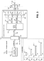
- FIG. 3 is a functional block diagram of the system controller 102 and switch controller 114 of FIG. 1 illustrating example command signals 118 from the system controller for different commands to adjust the conductivity modulated device 106 and/or the switch controller 114. It should be appreciated that the system controller 102, switch controller 114 and their respective elements couple and function as described above.
- the command signal 118 is a rectangular pulse waveform with high and low sections. As will be discussed, the duration of the low sections corresponds with which command is being transmitted by the system controller 102, referred to as active low pulse duration encoding. Under default conditions or steady state conditions, when no command is being sent, the command signal 118 is substantially equal to the high value. In one example, the high value could be substantially 5 volts (V). When the system controller 102 sends a command to the switch controller 114 via the command signal 118, the command signal transitions to a low value. In one example, the low value could be substantially 0V. The duration of the low value section of the command signal 118 corresponds to which command is being sent by the system controller 102. The example command signal 118 in FIG. 3 is an "active low" signal in which the duration of the low section corresponds to which command is being transmitted. However, it should be appreciated that the command signal 118 may be an "active high” signal in which the duration of the high section corresponds to which command is being transmitted.
- a first command 360 corresponds to the command signal 118 being substantially the low value for a period T.
- the command signal 118 could be substantially the low value for a period 2T.
- the low section of the second command 361 is twice as long as the low section for the first command 360.
- the command signal 118 could be substantially the low value for a period 3T for the third command 362, which is three times as long as the low section of the first command 360.
- the command signal 118 could be substantially the low value for a period 4T, which is four times as long as the low section of the first command 360.
- the duration of each command could be a period T longer than the duration of the previous command.
- the interface 120 could include a timer or counter to measure the durations of the low value sections in the command signal 118 to determine which command has been received.
- Example commands could include: status inquiry, reset, increase drive current, and decrease drive current.
- the increase drive current and decrease drive current commands are adjustment commands/signals to adjust the drive characteristics of the conductivity modulated device 106.
- the system controller 102 could send a "status inquiry" command in which the system controller 102 pings the switch controller 114 for the "status" of. of the switch controller 114, such as the information stored in a status register of the switch controller
- the system controller 102 could send a "reset" command in which the system controller 102 allows the switch controller 114 to be restarted or turned on.
- the system controller 102 could send an adjustment command to "increase drive current" in which the system controller 102 indicates that the switch controller 114 should increase either the current I EN of current source 140 or current I DIS of current source 144, or both, to decrease the rise time of the drain current I D 148 or the fall time of the drain current I D 148, or both (i.e. the fall time of the drain-source voltage V DS 150 or the rise time of the drain-source voltage V DS 150, or both).
- the decreased rise time or fall time would shorten the turn-on time or turn-off time, respectively, of the conductivity modulated device 106.
- the drive characteristic control 122 outputs the enable trim signal 132 and the disable trim signal 136 such that the current I EN of current source 140 and current I DIS of current source 144 are substantially equal to the first current value I 1 (of FIGS. 2A and 2B ).
- the system controller 102 outputs the third command 362 in response to the sense signal 115 indicating that there is a power event in the system 100 in which the system controller 102 may want to deliver more power.
- the drive characteristic controller 122 could output either the enable trim signal 132 or the disable trim signal (or both) to adjust the value of current I EN of current source 140 or current I DIS of current source 144 (or both) to the second current value I 2 (as shown in FIGS. 2A and 2B ) and increasing the drive current of the conductivity modulated device 106.
- the system controller 102 could send an adjustment command to "decrease drive current” (or in other words a "return drive current” command) in which the system controller 102 indicates that the switch controller 114 should decrease (or return) either the current I EN of current source 140 or current I DIS of current source 144, or both, to increase the rise time of the drain current I D 148 or the fall time of the drain current I D 148, or both (i.e. increase the fall time of the drain-source voltage V DS 150 of the rise time of the drain-source voltage V DS 150, or both).
- the system controller 102 indicates that the switch controller 114 should return the value of current I EN of current source 140 or current I DIS of current source 144, or both, to the first current value I 1 of FIGS. 2A and 2B .
- the sense signal 115 indicates to the system controller 102 that the increased power event in the system 100 has passed.
- the drive characteristic controller 122 could output either the enable trim signal 132 or the disable trim signal (or both) to adjust the value of current I EN of current source 140 or current I DIS of current source 144 (or both) to the first current value I 1 of FIGS. 2A and 2B and decreases (or returns) the drive current of the conductivity modulated device 106 to its default current value.
- the commands: status inquiry, reset, increase drive current, and decrease drive current are the first, second, third, and fourth commands 360, 361, 362, and 363, respectively, it should be appreciated that the commands could be in any order.
- the communication between the system controller 102 and the switch controller 114 may be bidirectional.
- the switch controller 114 may sense a fault condition (such as overcurrent, overvoltage, overheating, etc) in the system 100 and communicates the fault to the system controller 102.
- the fault communication from the switch controller 114 may be encoded as a multi-bit word to the system controller 102.
- FIG. 4 illustrates the switch controller 114 receiving the command signal 118 in response to a toggle 465, in accordance with embodiments of the present disclosure.
- the toggle 465 could be in response to a user.
- the toggle 465 could be in response to a dedicated hardware sensor which senses the power event.
- the switch controller 114 and its elements couple and function as described above.
- the switch controller 114 may receive commands from both the system controller (not shown) and the toggle 465.
- the switch controller 114 receives the command signal 118 in response to just the toggle 465.
- the user 465 may be a rectangular pulse waveform of logic high and logic low sections.
- the toggle 465 is representative of a user manually selecting from two choices, such as a mechanical switch.
- a logic low value for the toggle 465 corresponds to the rise time/fall time of the drain current I D 148 (rise time/fall time of the drain-source voltage V DS 150) substantially equal to a first value, as for example, the gate current I G 146 substantially equal to the first current value I 1 as shown in FIGS. 2A and 2B .
- a logic high value for the toggle 465 could correspond to the rise/fall time of the drain current I D 148 (rise time/fall time of the drain-source voltage V DS 150) substantially equal to a second value, as for example, the gate current IG 146 substantially equal to the second current value I 2 as shown in FIGS. 2A and 2B .
- a transistor 464 is coupled to the interface 120 of the switch controller 114 and the return 127.
- the control terminal of the transistor 464 is configured to receive the toggle 465.
- the transistor 464 is a bipolar junction transistor (BJT).
- BJT bipolar junction transistor
- the base of the transistor 464 is configured to receive the toggle 465, the emitter of transistor 464 is coupled to the return 127 and the collector of the transistor 464 is coupled to the interface 120.
- the command signal 118 is a voltage signal and is the collector voltage or the collector-emitter voltage of transistor 464. In operation, when the toggle 465 is low, the transistor 464 is off and the command signal 118 is high.
- a high value for the command signal 118 corresponds to the rise time/fall time of the drain current I D 148 (rise time/fall time of the drain-source voltage V DS 150) substantially equal to the first value.
- the toggle 465 is high, the transistor 464 is on and the command signal 118 is substantially equal to the return 127 (i.e. low value).
- a low value for the command signal 118 corresponds to the rise time/fall time of the drain current I D 148 (rise time/fall time of the drain-source voltage V DS 150) substantially equal to the second value.
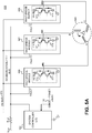
- FIG. 5A illustrates a multi-phase motor drive system 500 including three half-bridge inverter modules 566, 567, and 568, coupled individually to a high-voltage (HV) bus 576 and controlled with a single system controller 102 to drive a motor 569, such as for example a single-phase or 3-phase motor.
- HV high-voltage
- each half-bridge inverter modules 566, 567, and 568 and the system controller 102 are referenced to return 127.
- the system controller 102 can adjust the drive characteristics of one or more switches of the various half-bridge inverter modules 566, 567, and 568, in accordance with the teachings of the present disclosure.
- each switch is represented by an n-type metal-oxide-semiconductor field effect transistor (MOSFET) and is a conductivity modulated device as discussed above.
- MOSFET metal-oxide-semiconductor field effect transistor
- Each half-bridge module 566, 567, 568 are individually coupled to the HV bus 576.
- Each half-bridge module 566, 567, 568 includes a high side switch 570, 571, 572, and a low side switch 573, 574, 575, respectively coupled together as a power converter or an inverter in a full-bridge configuration.
- Each switch 570, 571, 572, 573, 574, and 575 is controlled by its own switch controller (shown further in FIG. 5B ) and form a power switching array.
- the half-bridge mid-point terminals HB1, HB2, HB3 between each high side and low side switch of their respective half-bridge modules 566, 567, 568, are coupled to the three phase terminals A, B, and C of the multiphase motor 569.
- the motor 569 is a brushless 3-phase DC motor, which may be included in for example an electric appliance, power tool, fan, or the like.
- the half-bridge modules 566, 567, and 568 provides the input electrical signals (such as voltage, current, frequency, and phase for the desired mechanical output load motion) to the motor 569 from the electrical energy supplied by the HV bus 576.
- switches 570, 570, 571, 572, 573, 574, and 575 are controlled by their respective switch controllers to regulate the energy flow to the motor 569.
- the switch controllers adjust the output to the motor 569 to maintain the target operation of the motor 569.
- the system controller 102 couples to each half-bridge module 566, 567, and 568 through the communication bus 577. Similar to above, in embodiments the system controller 102 receives a sense signal 116 representative of a power event.
- the power event may be an indication to the system controller 102 to adjust one or more drive characteristics of one or more of switches 570, 570, 571, 572, 573, 574, and 575.
- the system controller adjusts the drive current of one or more of switches 570, 570, 571, 572, 573, 574, and 575 in response to the sensed power event 116.
- the power event may indicate to the system controller 102 to decrease switch turn-on time and/or turn-off time by increasing the magnitude of the gate current IG 146 of one or more of switches 570, 570, 571, 572, 573, 574, and 575 to increase the rise time and/or fall time of the drain current I D 148 of one or more of switches 570, 570, 571, 572, 573, 574, and 575.
- a sensed power event which would increase the magnitude of the gate current IG 146 could include an outdoor air conditioning fan during startup that may have to overcome possible wind blowing conditions.
- a sensed power event could include a dishwasher water pump which has to pump a large amount of water in case the drain for the dishwasher has unexpectedly flooded.
- a further example of a sensed power event could include a refrigerator during initial installation to cool itself to the desired temperature.
- the system controller 102 is configured to output a command signal to one or more half-bridge modules 566, 567, and 568.
- the system controller 102 can send the command signal via the communication bus 577.
- the system controller 102 sends the command signal via a separate connection.
- the command signal 118 could be a voltage signal or a current signal.
- the command signal 118 could be representative of a digital word.
- the system controller 102 could apply coding to the command signal 118.
- the system controller 102 outputs a command signal 118 to at least one switch controller of one or more half-bridge modules 566, 567, and 568 via the communication bus 577.
- the command signal is outputted in response to the received sense signal 116 and may be representative of commands by the system controller 102 for the respective switch controller.
- Example commands communicated by the system controller 102 could include a "status inquiry" command for one or more of the half-bridge modules 566, 567, and 568.
- Another example command communicated by the system controller 102 could include a "fault” command in which the system controller 102 has sensed a fault condition (such as overcurrent, overvoltage, overheating, etc) in the system 100 and communicates the fault to half-bridge modules 566, 567, and 568.
- the half-bridge modules 566, 567, and 568 respond to the fault command by turning off their respective high-side and low-side switches.
- the system controller 102 communicates a command signal 118, representative of the drive characteristics of one or more of the high-side switches 570, 571, 572 and low-side switches 573, 574, and 575.
- An example drive characteristic includes the magnitude of the gate current IG 146 for the respective switch, which is related to the rise time and/or fall time of the drain current I D 148 and drain-to-source voltage 150 for the respective switch.
- Another example drive characteristic could include the duration which one or more of switches 570, 571, 572 573, 574, and 575 is driven by the gate current I G 146.
- the command communicated via the communication bus 577 could be representative of driving one or more of switches 570, 571, 572 573, 574, and 575 at a first magnitude of gate current IG or a second magnitude of gate current I G , where the second magnitude is greater than the first magnitude.
- the command signal 118 could represent driving one or more of switches 570, 571, 572 573, 574, and 575 with more than two magnitudes of gate current I G .
- Half-bridge modules 566, 567, and 568 are coupled to a communication bus 577, which is also coupled to system controller 102.
- the communication bus 577 which in one example is an open collector configuration, is coupled to a supply voltage V UP through a pull up resistor R UP . Further, the communication bus 577 may be in one example, a single-wire communication bus. As mentioned above, the communication bus 577 may be utilized by the system controller 102 to communicate commands to one or more half-bridge modules 566, 567, and 568. In one example, the communication bus 577 in normal steady state condition is pulled up to supply voltage V UP , and during any communication can be pulled down by the system controller 102 for sending a command to half-bridge modules 566, 567, and 568.
- the communication bus 577 can be pulled down for a detection of a command through a digital multi-bit word. In another embodiment, the communication bus 577 can be pulled down to communicate a command as discussed with respect to FIG. 3 . In some embodiments, the duration which the communication bus 577 is pulled down corresponds with the command sent by the system controller 102.
- FIG. 5B provides increased detail of the half-bridge modules in accordance with embodiments of the present disclosure. Specifically, FIG. 5B illustrates the half-bridge module 566, but it should be appreciated that the other half-bridge modules 567, 568, although present, are not shown in detail. Further the elements included in half-bridge modules 567, 568 are similar to what is shown in FIG. 5B with regards to half-bridge module 566.
- Half-bridge module 566 includes high-side switch 570 and low-side switch 537 coupled together in series.
- the high-side switch 570 and low-side switch 537 are exemplified by n-type MOSFETs with their respective body diodes.
- the drain of the high-side switch 570 is coupled to the HV bus 576 and the source of the source of low-side switch 573 is coupled to return 127.
- the half-bridge mid-point HB1 is coupled to phase A of motor 569.
- Half-bridge module 566 further includes switch controllers 114 and 515.
- Switch controller 114 is coupled to control the low-side switch 573 while switch controller 515 is coupled to control the high-side switch 570.
- Both switch controllers 114, 515 include drive characteristic control for their respective switches, as discussed above and in accordance with embodiments of the present disclosure.
- the switch controllers 114 and 515 can also include interfaces to receive the command signal 118, as will be further discussed. Similar to above, switch controllers 114, 515 control the enabling and disabling, along with the turn-on time and turn-off time of their respective switches. Further, the switch controllers 114, 515 can adjust the drive characteristics of the low-side switch 573 and the high-side switch 570, respectively, in response to the system controller 102.
- the system controller 102 is coupled to half-bridge module 566 and switch controller 114. As shown, the system controller 102 outputs the command signal 118 to the switch controller 114. In response to the command signal 118 received from the system controller 102, the switch controller 114 adjusts the drive characteristics of the low-side switch 537. In one embodiment, the interface (not shown) of the switch controller 114 receives the command signal 118 and outputs the drive characteristic signal to the drive characteristic control of switch controller 114. The drive characteristic control then outputs signals to the drive elements which enable and disable the low-side switch 573. The system controller 102 may send the command signal 118 via the communication bus 577 or by another coupling to switch controller 114.
- the system controller 102 can optionally be coupled to switch controller 515 to provide the command signal 118 rather than providing the command signal 118 via the switch controller 114.
- the switch controller 515 adjusts the drive characteristics of the high-side switch 570.
- the interface (not shown) of the switch controller 515 receives the command signal 118 and outputs the drive characteristic signal to the drive characteristic control of switch controller 515.
- the drive characteristic control then outputs signals to the drive elements which enable and disable the high-side switch 570.
- the system controller 102 may send the command signal 118 by another coupling to switch controller 515 or via the communication bus 577.
- switch controller 114 couples to switch controller 515.
- the switch controller 114 sends either the received command signal 118 or the drive characteristic signal 128 to switch controller 515 rather than the switch controller 515 receiving the command signal 118 from the system controller 102.
- Communication from the low-side switch controller 114 to the high-side switch controller 515 may be accomplished through communication links between the low-side switch controller 114 and the high-side controller 515.
- the control signals for controlling both the high-side switch 570 and low-side switch 573 may be received by the low-side switch controller 114 from the system controller 102.
- the control signal for switching the high-side switch 570 may be communicated to the high-side controller 515 from the low-side switch controller 114 via communication links.
- the low-side switch controller 114 relays the command signal 118 received from the system controller 102 to adjust the drive characteristics of the high side switch 570, such as the high-side drive current, to the high-side switch controller 515.
- the high-side switch controller 515 includes the interface (not shown) to receive the command signal 118 from the low-side switch controller 114 and outputs the drive characteristic signal to the drive characteristic control of switch controller 515. The drive characteristic control then outputs signals to drive elements which enable and disable the high-side switch 570.
- the low-side switch controller 114 receives the command signal 118 to adjust the drive characteristics of the high side switch 570, such as the high-side drive current, at an interface (not shown).
- the interface (not shown) outputs the drive characteristic signal 128 to adjust the drive characteristics of the high side switch 570 and the drive characteristic signal 128 of the low-side switch controller 114 is communicated to the high-side switch controller 515.
- the high-side switch controller 515 includes its own drive characteristic control which is coupled to and receives the drive characteristic signal 128 of the low-side switch controller 114.
- the drive characteristic control of switch controller 515 then outputs signals to drive elements which enable and disable the high-side switch 570.
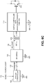
- FIG. 6A illustrates an example power converter 600 with switch controllers 114, 615 which include drive characteristic control in accordance with embodiments of the present disclosure.
- Switch controllers 114, 615 include drive characteristic control which is responsive to the system controller 102. Further, the system controller 102 can adjust the drive characteristics of switches 679, 680, in accordance with embodiments of the present disclosure.
- Power converter 600 receives an input voltage V IN 602 and is designed to transfer electrical energy form an input to a load 682 through an energy transfer element L1 681 by controlling the switching of power switches 679, 680. In various implementations, the power converter 600 can control the voltage, current, or power levels of the energy output to the load 682. In the example shown in FIG.
- Switch controller 114 may be referred to as a low-side switch controller while switch controller 615 may be referred to as a high-side switch controller.
- power switches 679, 680 are IGBTs.
- examples of the present invention can also be used in combination with other power switch technologies.
- MOSFETs metal-oxide-semiconductor field-effect transistors
- IEGTs injection enhancement gate transistors
- GTOs gate turn-off thyristors
- power converter 600 can be used with power switches which are based on gallium nitride (GaN) semiconductors or silicon carbide (SiC) semiconductors.
- System controller 102 is coupled to receive system inputs 699, sense signal 116 and provides the command signal 118.
- the system controller 102 determines whether the switch controllers 114, 615 should turn on or turn off the power switches 679, 680 based on system inputs 699.
- Example system inputs 699 include pulse width modulated (PWM) signal for a general purpose motor drive, a turn-on and turn-off sequence of a multi-level power converter, or a system fault turn-off request.
- PWM pulse width modulated
- the sense signal 116 is also a system input and in one embodiment is representative of a power event. In one embodiment, the power event may be an indication to the system controller 102 to adjust the drive characteristic of either power switch 679, 680 or both.
- the power event may be an indication to increase the drive current of either power switch 679, 680 or both.
- the power event may indicate to the system controller 102 to decrease turn-on time and/or turn-off time by increasing the magnitude of the control current for either power switch 679, 680 or both to increase the rise time and/or fall time of the current conducted by either power switch 679, 680 or both.
- system controller 102 outputs a command signal 118 representative of one or more commands to the interface 120 of switch controllers 114, 615.
- Example commands include enabling or disabling power switches 679, 680, reset, fault notification, and adjust the drive current (i.e. rise time and/or fall time of conducted current) of power switches 679, 680.
- the command signal 118 could be a voltage signal or a current signal.
- the command signal 118 could be representative of an N-bit digital word.
- the system controller 102 could apply coding to the command signal 118.
- the communication between the system controller 102 and the interface 120 may be bidirectional.
- Interface 120 is coupled to the system controller 102 and receives the command signal 118.
- FIG. 6A illustrates a single interface 120 for both the switch controllers 114, 615. However, it should be appreciated that each switch controller 114, 615 may have its own interface and as such the system controller 102 would output the command signal 118 to both interfaces.
- the interface 120 and the system controller 102 are both referenced to a primary reference potential 683 while the switch controller 114 is referenced to a secondary reference potential 684 and the switch controller 615 is referenced to a secondary reference potential 685. Secondary reference potentials 684, 685 are different potentials.
- reference potential 685 is coupled to the half-bridge point between the high-side switch 679 and the low-side switch 680 while reference potential 684 is coupled to the emitter of low-side switch 680.
- the switch controllers 114, 615 are galvanically isolated from the interface 120 by isolated communication links 678.
- the isolated communication links 678 may be implemented as an inductive coupling, such as a signal transformer or coupled inductor, optical coupling, or capacitive coupling. Further, the switch controllers 114, 615 may bidirectionally communicate with the interface 120 via the communication links 678.
- Interface 120 interprets the command signal 118 sent by the system controller 102 and sends the drive characteristic signal to switch controllers 114, 615 to drive the power switches 679, 680 and further, to adjust the drive current of power switches 679, 680.
- the switch controllers 114, 615 receive their respective drive characteristic signals and generate drive signals to control the power switches 670, 680.
- the switch controllers 114, 615 include drive characteristic control circuits and enable and disable drive elements to control the drive current (i.e. drive strength) of power switches 680, 679. As such, the system controller 102 adjusts the drive strength of power switches 680, 679.
- FIG. 6B illustrates another example of a power converter 601 in a half-bridge configuration with a system controller 102 to adjust the drive characteristics, such as for example the drive current, of power switches 679, 680.
- the power converter 601 shares many similarities with the power converter 600 shown in FIG. 6B . At least one difference however, is the interface 120 couples to switch controller 114 through isolation interface 678 and does not couple to the switch controller 615.
- interface 120 interprets the command signal 118 and outputs the drive characteristic signal 128 to the switch controller 114.
- the switch controller 114 sends the drive characteristic signal 128 to switch controller 615 rather than the switch controller 815 receiving the drive characteristic signal from interface 120.
- Communication from the low-side switch controller 114 to the high-side switch controller 615 may be accomplished through communication links between the low-side switch controller 114 and the high-side controller 615.
- the high-side switch controller 615 includes its own drive characteristic control which is coupled to and receives the drive characteristic signal 128 of the low-side switch controller 114.
- the drive characteristic control of switch controller 615 then outputs signals to drive elements which enable and disable the high-side switch 679.
- FIG. 6C illustrates an example isolated communication link 678.
- the interface 120 and the system controller 102 are both referenced to a primary reference potential 683 while the switch controller 114 is referenced to a secondary reference potential 684.
- the switch controller 114 is galvanically isolated from the interface 120 by isolated communication links 678.
- the isolated communication links 678 illustrated is a signal transformer with a primary winding 687 and a secondary winding 689.
- the interface 120 is coupled to the primary winding 687 and outputs the drive characteristic signal 128.
- the switch controller 114 is coupled to the secondary winding 689 and receives the drive characteristic signal 128 multiplied by the turns ratio of the primary and secondary windings 687, 689.
Landscapes
- Engineering & Computer Science (AREA)
- Power Engineering (AREA)
- Power Conversion In General (AREA)
- Electronic Switches (AREA)
- Inverter Devices (AREA)
Abstract
Description
- The present invention relates generally to a switch controller for a semiconductor switch, and more specifically to a switch controller which may be controlled by a user or a system controller.
- Household and industrial appliances such as ventilation fans, cooling systems, refrigerators, dishwashers, washer/dryer machines, and many other white products/goods typically utilize electric motors that transfer energy from an electrical source to a mechanical load. Electrical energy for driving the electric motors is provided through a drive system, which draws electrical energy from an electrical source (e.g., from an ac low frequency source). The electrical energy received from the electrical source is processed through a power converter, and converted to a desired form of electrical energy that is supplied to the motor to achieve the desired mechanical output. The desired mechanical output of the motor may be for example the speed of the motor, the torque, or the position of a motor shaft.
- Motors and their related circuitries such as motor drives represent a large portion of utility network loads. The functionality, efficiency, size, and price of motor drives are challenging and are competitive factors that suppliers of these products consider. The function of a power converter in a motor drive includes providing the input electrical signals to the motor such as voltage, current, frequency, and phase for a desired mechanical output load motion (e.g., spin/force) on the motor shaft. The power converter in one example may be an inverter transferring a dc input to an ac output of desired voltage, current, frequency, and phase and generally includes one or more switches to control the transfer of energy. Each switch is controlled by a switch controller for the power converter.
- Non-limiting and non-exhaustive embodiments of the present invention are described with reference to the following figures, wherein like reference numerals refer to like parts throughout the various views unless otherwise specified.
-
FIG. 1 is a functional block diagram of a system with a system controller which adjusts the drive characteristics of a switch in accordance with embodiments of the present disclosure. -
FIG. 2A is a timing diagram of various waveforms of the system ofFIG. 1 during a switch turn on event, in accordance with embodiments of the present disclosure. -
FIG. 2B is another timing diagram of various waveforms of the system ofFIG. 1 during a switch turn off event, in accordance with embodiments of the present disclosure. -
FIG. 3 is a functional block diagram of the system controller and switch controller ofFIG. 1 illustrating example commands from the system controller to adjust the switch, in accordance with embodiments of the present disclosure. -
FIG. 4 is a functional block diagram of a switch controller illustrating receiving commands from a user, in accordance with embodiments of the present disclosure. -
FIG. 5A is a functional block diagram of a motor driver with a system controller to adjust one or more switches of various half-bridge modules, in accordance with embodiments of the present disclosure. -
FIG. 5B is a functional block diagram of the system controller and half-bridge module ofFIG. 5A , in accordance with embodiments of the present disclosure. -
FIG. 6A is a functional block diagram of one example of a power converter in a half-bridge configuration with a system controller to adjust one or more switches, in accordance with embodiments of the present disclosure. -
FIG. 6B is a functional block diagram of another example of a power converter in a half-bridge configuration with a system controller to adjust one or more switches, in accordance with embodiments of the present disclosure. -
FIG. 6C is a functional block diagram of the system controller, interface, and switch controller ofFIGS. 6A and6B , in accordance with embodiments of the present disclosure. - Corresponding reference characters indicate corresponding components throughout the several views of the drawings. Skilled artisans will appreciate that elements in the figures are illustrated for simplicity and clarity and have not necessarily been drawn to scale. For example, the dimensions of some of the elements in the figures may be exaggerated relative to other elements to help to improve understanding of various embodiments of the present invention. Also, common but well-understood elements that are useful or necessary in a commercially feasible embodiment are often not depicted in order to facilitate a less obstructed view of these various embodiments of the present invention.
- In the following description, numerous specific details are set forth in order to provide a thorough understanding of the present invention. It will be apparent, however, to one having ordinary skill in the art that the specific detail need not be employed to practice the present invention. In other instances, well-known materials or methods have not been described in detail in order to avoid obscuring the present invention.
- Reference throughout this specification to "one embodiment", "an embodiment", "one example" or "an example" means that a particular feature, structure or characteristic described in connection with the embodiment or example is included in at least one embodiment of the present invention. Thus, appearances of the phrases "in one embodiment", "in an embodiment", "one example" or "an example" in various places throughout this specification are not necessarily all referring to the same embodiment or example. Furthermore, the particular features, structures or characteristics may be combined in any suitable combinations and/or subcombinations in one or more embodiments or examples. Particular features, structures or characteristics may be included in an integrated circuit, an electronic circuit, a combinational logic circuit, or other suitable components that provide the described functionality. In addition, it is appreciated that the figures provided herewith are for explanation purposes to persons ordinarily skilled in the art and that the drawings are not necessarily drawn to scale.
- In the context of the present application, when a transistor is in an "off state", or "off", the transistor does not substantially conduct current. Conversely, when a transistor is in an "on state", or "on", the transistor is able to substantially conduct current. By way of example, in one embodiment, a high-voltage transistor comprises an N-channel metal-oxide-semiconductor field-effect transistor (NMOS) with the high-voltage being supported between the first terminal, a drain, and the second terminal, a source. In another embodiment, a high-voltage transistor comprises an insulated-gate bipolar transistor (IGBT) with the high-voltage being supported between the first terminal, a collector, and the second terminal, an emitter. For purposes of this disclosure, "ground" or "ground potential" refers to a reference voltage or potential against which all other voltages or potentials of an electronic circuit or integrated circuit (IC) are defined or measured. In one example, the transistor or switch may also be referred to as a conductivity modulated device which may be controlled to conduct various amounts of current.
- Inverters with half-bridge switching configurations are commonly used with motor drives. Instead of implementing a full bridge switching configuration, utilizing a half-bridge switching circuit with low-side and high-side control blocks (also referred to as a low-side switch controller and high-side switch controller) inside one single package (e.g., a module) allows support for multiphase inverters, such as single-phase and 3-phase inverters, that provide increased layout flexibility as well as simplified thermal management for each module. Utilization of a modular half-bridge circuit structure for a motor drive inverter may reduce overall system cost because of a variety of reasons. Each switch of the half-bridge circuit structure is generally controlled by a switch controller which in turn is controlled by a system controller. The switches are controlled by the switch controllers to regulate the energy delivery in response to signals received from the system controller and/or a user.
- Conductivity modulated devices, such as transistors, maybe be utilized for the one or more switches in a power converter, such as an inverter. Typical losses related to conductivity modulated devices are conduction losses and switching losses (also referred to as crossover losses). When the conductivity modulated device conducts current, the voltage across the conductivity modulated device in response to the current through the conductivity modulated device generates conduction loss. Switching losses are generally associated with the losses, which occur while the conductivity modulated device is transitioning between an ON state and an OFF state or vice versa.
- In general, a conductivity modulated device takes time to transition from an ON state to an OFF state and vice versa in response to a drive signal that is provided to a control terminal of the conductivity modulated device. The control terminal of a field effect transistor (FET), insulated-gate bipolar transistor, or a SiC based transistor is generally referred to as the gate terminal. The control terminal of a bipolar junction transistor (BJT) is generally referred to as the base terminal. The time for the conductivity modulated device to transition from an OFF state to an ON state may be referred to as the turn-on time whereas the time for the conductivity modulated device to transition from an ON state to an OFF state may be referred to as the turn-off time. Switching/crossover losses occur during this transition time, and they may be lessened by reducing the duration of the turn-on and turn-off times. In addition, shorter turn-on and turn-off times generally correspond to reduced temperature of the conductivity modulated device (and therefore the system). However, shorter turn-on and turn-off times also generally correspond with increased system level electromagnetic interference (EMI). As such, there is generally a trade-off between EMI, switching losses, and temperature.
- The duration of the turn-on and turn-off time of a conductivity modulated device is related to the characteristics of the drive signal provided to the control terminal of the conductivity modulated device. It should be appreciated that conductivity modulated devices may be voltage controlled or current controlled at the gate terminal. Voltage controlled conductivity modulated devices typically would be controlled with a voltage source and a drive resistor (also referred to as a gate resistor) and the drive current for the conductivity modulated device is determined by the voltage drop across the control resistor. In other words, the value of the voltage source controls the drive characteristics of the conductivity modulated device. Current controlled conductivity devices could include a current source and the drive current for the conductivity modulated device is determined by the charge delivered by the current source. In other words, the value of the current source controls the drive characteristics of the conductivity modulated device. In one example, the drive signal is a current characterized by its magnitude, direction, and rate of change. The characteristics of the drive current determine the electric charge that passes through the control terminal of the conductivity modulated device, and it is the electric charge that ultimately modulates the conductivity of the conductivity modulated device. Drive current of higher magnitude corresponds to more charge in less time at the control terminal, resulting in shorter turn-on and/or turn-off time and lower switching/crossover losses. There may be conditions in a system, such as a motor drive, where the system controller could determine a need to deliver more power temporarily to a load without exceeding a maximum allowable temperature of the switching devices. The controller can reduce the turn-on and/or turn-off times of the switching devices to provide the temporary increase in power. Further, the system can be configured to tolerate higher electrical noise for the time the higher power is required. In embodiments of the present invention, the characteristics of a driver for a conductivity modulated device may be adjusted by a system controller and/or a user through the switch controller and/or a dedicated hardware sensor. The adjusted drive could increase or decrease the power delivered to the load within the bounds of other system parameters. In other words, a user and/or a system controller could adjust the drive characteristics of a conductivity modulated device to meet changing requirements. This could be accomplished by a switch controller which includes a drive characteristic control which can receive a drive characteristic signal representative of one or more drive characteristics of the conductivity modulated device. Further, in one embodiment, the conductivity modulated device may be adjusted in real time by a system controller and/or a user and as such, the drive characteristics of a conductivity modulated device may be adjusted on demand to meet changing requirements.
-
FIG. 1 illustrates asystem 100 with asystem controller 102 which adjusts the drive characteristics of a conductivity modulateddevice 106, in accordance with embodiments of the present disclosure.System 100 includes asystem controller 102 and apower switching array 104. Thepower switching array 104 can include one or more conductivity modulated devices. As shown, thepower switching array 104 includes conductivity modulateddevices devices power switching array 104 could be coupled in various configurations. For example, the conductivity modulated devices in thepower switching array 104 could be representative of transistors of one or more inverters with half-bridge switching configurations or other power converter topologies. In another example, the conductivity modulated devices in thepower switching array 104 could be representative of one or more inverter transistors with full-bridge switching configurations. - Each conductivity modulated
device switch controller 114 for conductivity modulateddevice 106 is illustrated. The voltage across the conductivity modulateddevice 106 is shown as voltage VDS 150 (also referred to as drain-source voltage VDS 150) while the conducted current of the conductivity modulateddevice 106 is current ID 148 (also referred to as drain current ID 148). In the example shown, the conductivity modulateddevice 106 is a current controlled device. The control current for the conductivity modulateddevice 106 is shown as current IG 146 (also referred to as gate current IG 146). The conductivity modulated device may be a transistor, such as a metal-oxide-semiconductor field-effect transistor (MOSFET), bipolar transistor, injection enhancement gate transistors (IEGT), insulated-gate bipolar transistor (IGBT) and gate turn-off thyristor (GTO). Further, the conductivity modulated device may be based on silicon (Si), gallium nitride (GaN), or silicon carbide (SiC) semiconductors. - The
system controller 102 couples to theswitch controller 114 throughinterface 120. In one example, theinterface 120 galvanically isolates thesystem controller 102 from theswitch controller 114. In another example, theinterface 120 does not galvanically isolate thesystem controller 102 from theswitch controller 114. As shown, thesystem controller 102 receives asense signal 116 representative of a power event. In one example, the power event may be an indication to thesystem controller 102 to provide increased power to a load, such as a motor. In one embodiment, the sensed power event may indicate to thesystem controller 102 to adjust the drive characteristics of the conductivity modulateddevice 106. In on example, thesystem controller 102 adjusts the drive characteristics of the conductivity modulateddevice 106 by increasing the magnitude of the drive current (e.g. gate current IG 146) of the conductivity modulateddevice 106. Further, in one embodiment thesystem controller 102 adjusts the drive characteristics of the conductivity modulateddevice 106 by increasing the magnitude of the drive current during either the turn-on time, the turn-off time, or both. In one example, the drive current may also be referred to as the drive strength with greater magnitude of drive currents corresponding to greater drive strength. Or in other words, the power event may indicate to thesystem controller 102 to decrease turn-on time and/or turn-off time by increasing the magnitude of the gatecurrent IG 146 to decrease the rise time and/or fall time of the drain current ID 148 of the conductivity modulateddevice 106. In some embodiments, the power event may indicate to thesystem controller 102 to decrease turn-on time and/or turn-off time by increasing the magnitude of the gatecurrent IG 146 to decrease the fall time and/or rise time of the drain-source voltage V DS 150. For example, thesystem controller 102 decreases turn-on time and/or turn-off time by modulating the value of currents IEN and IDIS ofcurrent sources current IG 146 could include an outdoor air conditioning fan during startup that may have to overcome possible wind blowing conditions. Another example of a sensed power event could include a dishwasher water pump which has to pump a large amount of water in case the drain for the dishwasher has unexpectedly flooded. A further example of a sensed power event could include a refrigerator during initial installation to cool itself to the desired temperature, also known as a cool-down period. - In the embodiment shown in
FIG. 1 ,system controller 102 outputs acommand signal 118 to theswitch controller 114. In one example, thecommand signal 118 is outputted in response to the receivedsense signal 116. Thecommand signal 118 is representative of one or more commands for theswitch controller 114 by thesystem controller 102 and vice versa. In one example, the communication between thesystem controller 102 and theswitch controller 114 is bidirectional. Example commands communicated by and/or to thesystem controller 102 could include a "status inquiry" command in which thesystem controller 102 pings theswitch controller 114 for the "status" of theswitch controller 114, such as the information stored in a status register of the switch controller. Another example command communicated with thesystem controller 102 could include a "fault" command in which theswitch controller 114 has sensed a fault condition (such as overcurrent, overvoltage, overheating, etc) in thesystem 100 and communicates the fault to thesystem controller 102. In general, theswitch controller 114 responds to a sensed fault by turning off the conductivity modulateddevice 106. A further example command communicated by thesystem controller 102 could include a "reset" command in which theswitch controller 114 is restarted or turned on. In embodiments of the present disclosure, thesystem controller 102 communicates an adjustment command representative of adjusting one or more drive characteristics of conductivity modulateddevice 106. An example drive characteristic includes the magnitude of the gate current IG 146 (e.g. drive strength) which is related to the rise time and/or fall time of the drain current ID 148 and the drain-source voltage V DS 150. The magnitude of the gatecurrent IG 146 may be varied by modulating the values of currents IEN and IDIS bycurrent sources device 106 is driven by the gatecurrent IG 146. A further example drive characteristic could include the frequency which the conductivity modulateddevice 106 is driven by the gatecurrent IG 146. For example, the gatecurrent IG 146 could be a pulsed signal which may be pulse width modulated (PWM) or pulse frequency modulated (PFM) in response to thecommand signal 118. In some embodiments, thecommand signal 118 could be representative of driving the conductivity modulateddevice 106 at a first magnitude of gatecurrent IG 146 or a second magnitude of gatecurrent IG 146, where the second magnitude is greater than the first magnitude. Thecommand signal 118 could be a voltage signal or a current signal. In one example, thecommand signal 118 could be representative of a digital word. Further, thesystem controller 102 could apply coding to thecommand signal 118. - The
interface 120 receives thecommand signal 118 and interprets/demodulates thecommand signal 118 to output the drivecharacteristic signal 128. In embodiments, the drivecharacteristic signal 128 is representative of one or more drive characteristics for the conductivity modulateddevice 106. Theswitch controller 114 also includes a drivecharacteristic control 122 and driveelements interface 120 is coupled to and outputs the drivecharacteristic signal 128 to the drivecharacteristic control 122. Drivecharacteristic control 122 is coupled to driveelements elements device 106. In embodiments, the drivecharacteristic control 122 controls driveelements characteristic signal 128. Further, the drivecharacteristic control 122 controls driveelements device 106 with the one or more drive characteristics provided by the drivecharacteristic signal 128. As shown inFIG. 1 , the drivecharacteristic control 122 outputs an enablesignal EN 130 and disablesignal DIS 134 to turn on or turn off the conductivity modulateddevice 106. In one example, theenable signal EN 130 and the disablesignal DIS 134 could be outputted in response to thecommand signal 118 from thesystem controller 102 via the drivecharacteristic signal 128. In another example, theenable signal EN 130 and the disablesignal DIS 134 could be outputted in response to one or more signals, separate fromcommand signal 118, received by theswitch controller 114. Further, the drivecharacteristic control 122 could receive the one or more signals, separate from thecommand signal 118, and outputs the applicable enablesignal EN 130 or disablesignal DIS 134 to turn on or turn off the conductivity modulateddevice 106 - As will be discussed further, in one embodiment the drive
characteristic control 122 adjusts the drive strength (e.g. drive current) of the conductivity modulateddevice 106 by adjusting the current provided bydrive elements characteristic control 122 outputs the enabletrim signal 132 and the disabletrim signal 136 to thedrive elements device 106. -
Drive element 124 includesswitch 138 andcurrent source 140 with current IEN to enable the conductivity modulateddevice 106.Current source 140 is coupled to the conductivity modulateddevice 106 to provide current to the control terminal (e.g. gate).Drive element 126 includesswitch 142 andcurrent source 144 with current IDIS to disable the conductivity modulateddevice 106.Current source 144 is coupled to the conductivity modulateddevice 106 to sink current from the control terminal (e.g. gate). In some embodiments,current sources characteristic signal 128. - Drive
characteristic control 122 is coupled to output an enablesignal EN 130 and an enabletrim signal 132 to driveelement 124. To enable the conductivity modulateddevice 106 to conduct (i.e. turn on), the drivecharacteristic control 122 outputs theenable signal EN 130 to turn on theswitch 138 and turns offswitch 140. The current IEN is sourced to the control terminal of the conductivity modulateddevice 106 and the magnitude of the gatecurrent IG 146 of the conductivity modulateddevice 106 is substantially equal to current IEN. In one example, theenable signal EN 130 may be a rectangular pulse waveform with varying lengths of logic high and logic low sections. Logic high sections could correspond to theswitch 138 being on while logic low sections could correspond to theswitch 138 being off (or vice versa). In one embodiment, the drivecharacteristic control 122 outputs theenable signal EN 130 in response to a signal separate from thecommand signal 118 and the drivecharacteristic signal 128. Drivecharacteristic control 122 outputs an enabletrim signal 132 to adjust the value of the current IEN and therefore the magnitude of the gatecurrent IG 146. In embodiments of the present disclosure enabletrim signal 132 is responsive to the drivecharacteristic signal 128. The enabletrim signal 132 may be a voltage or current signal, with the magnitude of the current IEN corresponding to the value of the enable trim signal. In one example of the present disclosure, the enabletrim signal 132 can trim the value of the current IEN to a first current value I1 or a second current value I2, however it should be appreciated that the enabletrim signal 132 can trim the value of the current IEN to a plurality of current values. The magnitude of the gatecurrent IG 146 controls the fall time of the drain-source voltage VDS 150 and the turn-on time of the conductivity modulateddevice 106 whenswitch 138 is on andcurrent source 140 is providing current to the conductivity modulateddevice 106 whileswitch 142 is off. As such, thesystem controller 102 can adjust the drive characteristics, such as the rise time of the drain current ID 148 and/or the fall time of the drain-source voltage V DS 150 and the turn-on time, of a conductivity modulateddevice 106. - Similarly, the drive
characteristic control 122 is configured to output a disablesignal DIS 134 and disabletrim signal 136 to driveelement 126. To disable the conductivity modulateddevice 106 from conducting (i.e. turn off), the drivecharacteristic control 122 outputs the disablesignal DIS 134 to turn on theswitch 142 and turns offswitch 138. The amount of current sinked from the control terminal of the conductivity modulateddevice 106 is limited by the value of current IDIS provided bycurrent source 144. In one example, the disablesignal DIS 134 is a rectangular pulse waveform with varying lengths of logic high or logic low sections. Logic high sections could correspond to theswitch 142 being on while logic low sections could correspond to theswitch 142 being off (or vice versa). In one example, the disablesignal DIS 134 is substantially the inverse of theenable signal EN 130. In one embodiment, the drivecharacteristic control 122 outputs the disablesignal DIS 136 in response to a signal separate from thecommand signal 118 and the drivecharacteristic signal 128. The drivecharacteristic control 122 outputs the disabletrim signal 136 to adjust the value of the current IDIS and therefore the magnitude of the gatecurrent I G 146. In embodiments of the present disclosure, disabletrim signal 136 is responsive to the drivecharacteristic signal 128. The disabletrim signal 136 may be a voltage or current signal, with the magnitude of the current IDIS corresponding to the value of the disabletrim signal 136. In one example of the present disclosure, the disabletrim signal 136 can trim the value of the current IDIS to a first current Ii value or a second current value I2, however it should be appreciated that the disabletrim signal 132 can trim the value of the current IDIS to a plurality of current values. The magnitude of the gate current IG 146 controls the fall time of the drain current ID 148 and the subsequent turn-off time of the conductivity modulateddevice 106. As such, thesystem controller 102 can adjust the drive characteristics, such as the fall time of the drain current ID 148 and the subsequent turn-off time, of a conductivity modulateddevice 106. - In another embodiment, the drive
characteristic control 122 may adjust the drive characteristics for the conductivity modulateddevice 106 by pulse width modulating or pulse frequency modulating theenable signal EN 130 or the disablesignal DIS 134. By pulse width modulating or pulse frequency modulating theenable signal EN 130 or the disablesignal DIS 134, the drivecharacteristic control 122 adjusts the average magnitude of the gatecurrent IG 146. As such the rise time and/or fall time of the drain-source voltage V DS 150 or the drain current ID 148 may be adjusted and subsequent turn-on and/or turn-off times of the conductivity modulateddevice 106. -
FIG. 2A illustrates an example timing diagram 200 of theenable signal EN 130, gate current IG 146, the drain-source voltage V DS 150 and draincurrent I D 148 during a turn-on transition of the conductivity modulateddevice 106 ofFIG. 1 . The example waveforms for the gatecurrent IG 146, draincurrent I D 148, and drain-source voltage V DS 150 shown inFIG. 2A are straight-line approximations. Further,FIG. 2A illustrates example waveforms for the gate current IG 146, draincurrent I D 148, and drain-source voltage V DS 150 for different drive strengths. The example waveforms on the right hand side of the page illustrate providing the conductivity modulateddevice 106 with greater drive current than the examples waveforms on the left hand side of the page. - In the example shown, the
enable signal EN 130 transitions from logic low to logic high to turn-on theswitch 138 ofdrive element 124. Similarly, the disable signal (not shown) would transition from logic high to logic low to turn offswitch 142. As such, the conductivity modulateddevice 106 is enabled to conduct a drivecurrent I D 148. - Once the
switch 138 is turned on (and switch 142 is turned off) by theenable signal EN 130, the gatecurrent IG 146 increases to the magnitude of current IEN ofcurrent source 140. On the left hand side of the page, current IEN ofcurrent source 140 is substantially equal to a first current value I1. - After the
switch 138 is turned on, the drain current ID 148 of the conductivity modulateddevice 106 increases from zero with slope mi. For the example shown, the draincurrent ID 148 increases to a peak value and then decreases to its conduction value. In the embodiment shown inFIG. 2A , the drain-source voltage V DS 150 of the conductivity modulateddevice 106 begins to decrease to zero with a slope m2 once the drain current ID 148 reaches its peak value. The magnitude of slopes m1 and m2 are related to the magnitude of the gate current IG, which for the example on the left hand side is substantially equal to the first current value I1 of current source IEN 140. For the example shown, the turn-ontime 252 begins when theenable signal EN 130 transitions to a logic high value and ends when the drain-source voltage V DS 150 is substantially zero and the drain current ID 148 of the conductivity modulated device 160 has reached its conduction value. - On the right hand side of the page, current IEN of
current source 140 is substantially equal to a second current value h. As shown, the second current value I2 is greater than the first current value I1. The magnitudes of slopes mi (for the drain current ID 148) and m2 (for the drain-source voltage VDS 150) are greater as compared to the magnitudes of slopes m1 and m2 shown on the left hand side of the page. As such, the rise time of for the drain current ID 148 is shorter (and the fall time for the drain-source voltage V DS 150 is shorter) resulting in an overall shorter turn-ontime 254 for the operation of the conductivity modulateddevice 106 on the right hand side as compared to the turn-ontime 252 shown on the left-hand side of the page. In other words, varying the value of the current IEN of thecurrent source 140 and subsequently the gate current IG 146 of the conductivity modulateddevice 106 varies the turn-on time of the conductivity modulateddevice 106. The shaded area under the waveforms for the drain current ID 148 and the drain-source voltage V DS 150 represents the crossover energy loss during the turn-on of the conductivity modulateddevice 106. As shown the shaded area on the left hand side of the page is larger than the right hand side of the page, indicating that the crossover losses for the conductivity modulateddevice 106 on the left hand side of the page is greater than on the right hand side of the page. Shorter turn-on times reduce switching/crossover losses, which also reduces the amount of dissipated heat and increases the amount of power delivery by thesystem 100. However, shorter turn-on times may lead to increase EMI. -
FIG. 2B illustrates an example timing diagram 201 of the disablesignal DIS 134, gatecurrent IG 146, the drain-source voltage V DS 150 and draincurrent I D 148 during a turn-off transition of the conductivity modulateddevice 106 ofFIG. 1 . Similar toFIG. 2A , the example waveforms for the gate current IG 146, draincurrent I D 148, and drain-source voltage V DS 150 shown are straight-line approximations. Further,FIG. 2B illustrates the example waveforms for the gate current IG 146, draincurrent I D 148, and drain-source voltage V DS 150 for different drive strengths. The example waveforms for the gate current IG 146, draincurrent I D 148, and drain-source voltage V DS 150 on the right hand side of the page has a greater drive current than the example waveforms for gate current IG 146, draincurrent I D 148, and drain-source voltage V DS 150 on the left hand side of the page. - The disable
signal DIS 134 transitions from logic low to logic high to turn-on theswitch 142 ofdrive element 126. Similarly, the enable signal (not shown) would transition from logic high to logic low to turn offswitch 138. As such, the conductivity modulateddevice 106 is disabled from conducting a drivecurrent I D 148. - Once the
switch 142 is turned on (and switch 138 is turned off) by the disablesignal DIS 134, the magnitude of the gatecurrent IG 146 is substantially the magnitude of current IDIS ofcurrent source 144. For thedrive element 126 shown inFIG. 1 , once theswitch 142 is turned on (and switch 138 is off) the gatecurrent IG 146 is flowing to return 127. Due to the direction of current, the gatecurrent IG 146 shown inFIG. 2B decreases. Further, the maximum magnitude of the gatecurrent IG 146 is responsive to the magnitude of current IDIS ofcurrent source 144. On the left hand side of the page, current IDIS ofcurrent source 144 is substantially equal to a first current value I1. - After the
switch 142 is turned on, the drain-source voltage V DS 150 of the conductivity modulateddevice 106 begins to increase from zero with a slope m2. For the example sown, the drain current ID 148 of the conductivity modulateddevice 106 decreases to zero with slope mi once the drain-source voltage V DS 150 has reached its peak value. The magnitude of slopes m1 and m2 are related to the magnitude of the gate current IG, which for the example on the left hand side is substantially equal to the first current value I1 of current source IDIS 144. For the example shown, the turn-off time 256 begins when the disablesignal DIS 134 transitions to a logic high value and ends when the the drain current ID 148 is substantially zero and the drain-source voltage V DS 150 of the conductivity modulated device 160 has reached its nonconducting value. - On the right hand side of the page, current IDIS of
current source 144 is substantially equal to a second current value h. As shown, the second current value I2 is greater than the first current value Ii. The magnitudes of slopes mi (for the drain current ID 148) and m2 (for the drain-source voltage VDS 150) are greater as compared to the magnitudes of slopes m1 and m2 shown on the left hand side of the page. As such, the fall time of for the drain current ID 148 is shorter (and the rise time for the drain-source voltage V DS 150 is shorter) resulting in an overall shorter turn-off time 258 for the operation of the conductivity modulateddevice 106 on the right hand side as compared to the turn-off time 256 shown on the left-hand side of the page. In other words, varying the value of the current IDIS of thecurrent source 144 and subsequently of the gate current IG 146 of the conductivity modulateddevice 106, the turn-off time of the conductivity modulateddevice 106 is shortened. The shaded area under the waveforms for the drain current ID 148 and the drain-source voltage V DS 150 represents the crossover loss during the turn-on of the conductivity modulateddevice 106. As shown the shaded area on the left hand side of the page is larger than the right hand side of the page, indicating that the crossover losses for the conductivity modulateddevice 106 on the left hand side of the page is greater than on the right hand side of the page. Shorter turn-off times reduce switching/crossover losses, which also reduces the amount of dissipated heat and increases the amount of power delivery by thesystem 100. -
FIG. 3 is a functional block diagram of thesystem controller 102 andswitch controller 114 ofFIG. 1 illustrating example command signals 118 from the system controller for different commands to adjust the conductivity modulateddevice 106 and/or theswitch controller 114. It should be appreciated that thesystem controller 102,switch controller 114 and their respective elements couple and function as described above. - As shown, the
command signal 118 is a rectangular pulse waveform with high and low sections. As will be discussed, the duration of the low sections corresponds with which command is being transmitted by thesystem controller 102, referred to as active low pulse duration encoding. Under default conditions or steady state conditions, when no command is being sent, thecommand signal 118 is substantially equal to the high value. In one example, the high value could be substantially 5 volts (V). When thesystem controller 102 sends a command to theswitch controller 114 via thecommand signal 118, the command signal transitions to a low value. In one example, the low value could be substantially 0V. The duration of the low value section of thecommand signal 118 corresponds to which command is being sent by thesystem controller 102. Theexample command signal 118 inFIG. 3 is an "active low" signal in which the duration of the low section corresponds to which command is being transmitted. However, it should be appreciated that thecommand signal 118 may be an "active high" signal in which the duration of the high section corresponds to which command is being transmitted. - For example, a first command 360 corresponds to the
command signal 118 being substantially the low value for a period T. For asecond command 361, thecommand signal 118 could be substantially the low value for aperiod 2T. In the example shown, the low section of thesecond command 361 is twice as long as the low section for the first command 360. Similarly for thethird command 362 and thefourth command 363. Thecommand signal 118 could be substantially the low value for aperiod 3T for thethird command 362, which is three times as long as the low section of the first command 360. For thefourth command 363, thecommand signal 118 could be substantially the low value for aperiod 4T, which is four times as long as the low section of the first command 360. In other words, the duration of each command could be a period T longer than the duration of the previous command. In one example, theinterface 120 could include a timer or counter to measure the durations of the low value sections in thecommand signal 118 to determine which command has been received. - Example commands could include: status inquiry, reset, increase drive current, and decrease drive current. The increase drive current and decrease drive current commands are adjustment commands/signals to adjust the drive characteristics of the conductivity modulated
device 106. For the first command 360, thesystem controller 102 could send a "status inquiry" command in which thesystem controller 102 pings theswitch controller 114 for the "status" of. of theswitch controller 114, such as the information stored in a status register of the switch controller - For the
second command 361, thesystem controller 102 could send a "reset" command in which thesystem controller 102 allows theswitch controller 114 to be restarted or turned on. - For the
third command 362, thesystem controller 102 could send an adjustment command to "increase drive current" in which thesystem controller 102 indicates that theswitch controller 114 should increase either the current IEN ofcurrent source 140 or current IDIS ofcurrent source 144, or both, to decrease the rise time of the drain current ID 148 or the fall time of the drain current ID 148, or both (i.e. the fall time of the drain-source voltage V DS 150 or the rise time of the drain-source voltage V DS 150, or both). The decreased rise time or fall time would shorten the turn-on time or turn-off time, respectively, of the conductivity modulateddevice 106. Under normal operating conditions, the drivecharacteristic control 122 outputs the enabletrim signal 132 and the disabletrim signal 136 such that the current IEN ofcurrent source 140 and current IDIS ofcurrent source 144 are substantially equal to the first current value I1 (ofFIGS. 2A and2B ). In one example, thesystem controller 102 outputs thethird command 362 in response to the sense signal 115 indicating that there is a power event in thesystem 100 in which thesystem controller 102 may want to deliver more power. In response to thethird command 362, the drivecharacteristic controller 122 could output either the enabletrim signal 132 or the disable trim signal (or both) to adjust the value of current IEN ofcurrent source 140 or current IDIS of current source 144 (or both) to the second current value I2 (as shown inFIGS. 2A and2B ) and increasing the drive current of the conductivity modulateddevice 106. - For the
fourth command 363, thesystem controller 102 could send an adjustment command to "decrease drive current" (or in other words a "return drive current" command) in which thesystem controller 102 indicates that theswitch controller 114 should decrease (or return) either the current IEN ofcurrent source 140 or current IDIS ofcurrent source 144, or both, to increase the rise time of the drain current ID 148 or the fall time of the drain current ID 148, or both (i.e. increase the fall time of the drain-source voltage V DS 150 of the rise time of the drain-source voltage V DS 150, or both). Or in other words, thesystem controller 102 indicates that theswitch controller 114 should return the value of current IEN ofcurrent source 140 or current IDIS ofcurrent source 144, or both, to the first current value I1 ofFIGS. 2A and2B . In one example, the sense signal 115 indicates to thesystem controller 102 that the increased power event in thesystem 100 has passed. In response to thefourth command 363, the drivecharacteristic controller 122 could output either the enabletrim signal 132 or the disable trim signal (or both) to adjust the value of current IEN ofcurrent source 140 or current IDIS of current source 144 (or both) to the first current value I1 ofFIGS. 2A and2B and decreases (or returns) the drive current of the conductivity modulateddevice 106 to its default current value. Although for this example, the commands: status inquiry, reset, increase drive current, and decrease drive current are the first, second, third, andfourth commands - In some embodiments, the communication between the
system controller 102 and theswitch controller 114 may be bidirectional. For example, theswitch controller 114 may sense a fault condition (such as overcurrent, overvoltage, overheating, etc) in thesystem 100 and communicates the fault to thesystem controller 102. The fault communication from theswitch controller 114 may be encoded as a multi-bit word to thesystem controller 102. -
FIG. 4 illustrates theswitch controller 114 receiving thecommand signal 118 in response to atoggle 465, in accordance with embodiments of the present disclosure. In one embodiment, thetoggle 465 could be in response to a user. In another embodiment, thetoggle 465 could be in response to a dedicated hardware sensor which senses the power event. It should be appreciated that theswitch controller 114 and its elements couple and function as described above. In one example, theswitch controller 114 may receive commands from both the system controller (not shown) and thetoggle 465. In another example, theswitch controller 114 receives thecommand signal 118 in response to just thetoggle 465. - The
user 465 may be a rectangular pulse waveform of logic high and logic low sections. In one embodiment, thetoggle 465 is representative of a user manually selecting from two choices, such as a mechanical switch. A logic low value for thetoggle 465 corresponds to the rise time/fall time of the drain current ID 148 (rise time/fall time of the drain-source voltage VDS 150) substantially equal to a first value, as for example, the gate current IG 146 substantially equal to the first current value I1 as shown inFIGS. 2A and2B . A logic high value for thetoggle 465 could correspond to the rise/fall time of the drain current ID 148 (rise time/fall time of the drain-source voltage VDS 150) substantially equal to a second value, as for example, the gatecurrent IG 146 substantially equal to the second current value I2 as shown inFIGS. 2A and2B . - As shown in one embodiment, a
transistor 464 is coupled to theinterface 120 of theswitch controller 114 and thereturn 127. The control terminal of thetransistor 464 is configured to receive thetoggle 465. In the embodiment shown, thetransistor 464 is a bipolar junction transistor (BJT). The base of thetransistor 464 is configured to receive thetoggle 465, the emitter oftransistor 464 is coupled to thereturn 127 and the collector of thetransistor 464 is coupled to theinterface 120. For the embodiment shown, thecommand signal 118 is a voltage signal and is the collector voltage or the collector-emitter voltage oftransistor 464. In operation, when thetoggle 465 is low, thetransistor 464 is off and thecommand signal 118 is high. As such, a high value for thecommand signal 118 corresponds to the rise time/fall time of the drain current ID 148 (rise time/fall time of the drain-source voltage VDS 150) substantially equal to the first value. When thetoggle 465 is high, thetransistor 464 is on and thecommand signal 118 is substantially equal to the return 127 (i.e. low value). As such, a low value for thecommand signal 118 corresponds to the rise time/fall time of the drain current ID 148 (rise time/fall time of the drain-source voltage VDS 150) substantially equal to the second value. -
FIG. 5A illustrates a multi-phasemotor drive system 500 including three half-bridge inverter modules single system controller 102 to drive amotor 569, such as for example a single-phase or 3-phase motor. As shown, each half-bridge inverter modules system controller 102 are referenced to return 127. Further, thesystem controller 102 can adjust the drive characteristics of one or more switches of the various half-bridge inverter modules - Each half-
bridge module bridge module high side switch low side switch switch FIG. 5B ) and form a power switching array. The half-bridge mid-point terminals HB1, HB2, HB3 between each high side and low side switch of their respective half-bridge modules multiphase motor 569. In one example, themotor 569 is a brushless 3-phase DC motor, which may be included in for example an electric appliance, power tool, fan, or the like. In operation, the half-bridge modules motor 569 from the electrical energy supplied by the HV bus 576. The switching properties ofswitches motor 569. In other words, the switch controllers adjust the output to themotor 569 to maintain the target operation of themotor 569. - The
system controller 102 couples to each half-bridge module system controller 102 receives asense signal 116 representative of a power event. In one embodiment, the power event may be an indication to thesystem controller 102 to adjust one or more drive characteristics of one or more ofswitches switches power event 116. Or in other words, the power event may indicate to thesystem controller 102 to decrease switch turn-on time and/or turn-off time by increasing the magnitude of the gatecurrent IG 146 of one or more ofswitches switches current IG 146 could include an outdoor air conditioning fan during startup that may have to overcome possible wind blowing conditions. Another example of a sensed power event could include a dishwasher water pump which has to pump a large amount of water in case the drain for the dishwasher has unexpectedly flooded. A further example of a sensed power event could include a refrigerator during initial installation to cool itself to the desired temperature. - The
system controller 102 is configured to output a command signal to one or more half-bridge modules system controller 102 can send the command signal via the communication bus 577. In another embodiment, thesystem controller 102 sends the command signal via a separate connection. Thecommand signal 118 could be a voltage signal or a current signal. In one example, thecommand signal 118 could be representative of a digital word. Further, thesystem controller 102 could apply coding to thecommand signal 118. As will be further illustrated with respect toFIG. 5B , thesystem controller 102 outputs acommand signal 118 to at least one switch controller of one or more half-bridge modules sense signal 116 and may be representative of commands by thesystem controller 102 for the respective switch controller. Example commands communicated by thesystem controller 102 could include a "status inquiry" command for one or more of the half-bridge modules system controller 102 could include a "fault" command in which thesystem controller 102 has sensed a fault condition (such as overcurrent, overvoltage, overheating, etc) in thesystem 100 and communicates the fault to half-bridge modules bridge modules - In embodiments of the present disclosure, the
system controller 102 communicates acommand signal 118, representative of the drive characteristics of one or more of the high-side switches side switches current IG 146 for the respective switch, which is related to the rise time and/or fall time of the drain current ID 148 and drain-to-source voltage 150 for the respective switch. Another example drive characteristic could include the duration which one or more ofswitches current I G 146. For example, the command communicated via the communication bus 577 could be representative of driving one or more ofswitches command signal 118 could represent driving one or more ofswitches - Half-
bridge modules system controller 102. The communication bus 577, which in one example is an open collector configuration, is coupled to a supply voltage VUP through a pull up resistor RUP. Further, the communication bus 577 may be in one example, a single-wire communication bus. As mentioned above, the communication bus 577 may be utilized by thesystem controller 102 to communicate commands to one or more half-bridge modules system controller 102 for sending a command to half-bridge modules FIG. 3 . In some embodiments, the duration which the communication bus 577 is pulled down corresponds with the command sent by thesystem controller 102. -
FIG. 5B provides increased detail of the half-bridge modules in accordance with embodiments of the present disclosure. Specifically,FIG. 5B illustrates the half-bridge module 566, but it should be appreciated that the other half-bridge modules bridge modules FIG. 5B with regards to half-bridge module 566. - Half-
bridge module 566 includes high-side switch 570 and low-side switch 537 coupled together in series. The high-side switch 570 and low-side switch 537 are exemplified by n-type MOSFETs with their respective body diodes. The drain of the high-side switch 570 is coupled to the HV bus 576 and the source of the source of low-side switch 573 is coupled to return 127. The half-bridge mid-point HB1 is coupled to phase A ofmotor 569. - Half-
bridge module 566 further includesswitch controllers Switch controller 114 is coupled to control the low-side switch 573 whileswitch controller 515 is coupled to control the high-side switch 570. Bothswitch controllers switch controllers command signal 118, as will be further discussed. Similar to above,switch controllers switch controllers side switch 573 and the high-side switch 570, respectively, in response to thesystem controller 102. - The
system controller 102 is coupled to half-bridge module 566 andswitch controller 114. As shown, thesystem controller 102 outputs thecommand signal 118 to theswitch controller 114. In response to thecommand signal 118 received from thesystem controller 102, theswitch controller 114 adjusts the drive characteristics of the low-side switch 537. In one embodiment, the interface (not shown) of theswitch controller 114 receives thecommand signal 118 and outputs the drive characteristic signal to the drive characteristic control ofswitch controller 114. The drive characteristic control then outputs signals to the drive elements which enable and disable the low-side switch 573. Thesystem controller 102 may send thecommand signal 118 via the communication bus 577 or by another coupling to switchcontroller 114. - As shown in a dashed line, in some embodiments the
system controller 102 can optionally be coupled to switchcontroller 515 to provide thecommand signal 118 rather than providing thecommand signal 118 via theswitch controller 114. In response to thecommand signal 118, theswitch controller 515 adjusts the drive characteristics of the high-side switch 570. In one embodiment, the interface (not shown) of theswitch controller 515 receives thecommand signal 118 and outputs the drive characteristic signal to the drive characteristic control ofswitch controller 515. The drive characteristic control then outputs signals to the drive elements which enable and disable the high-side switch 570. Thesystem controller 102 may send thecommand signal 118 by another coupling to switchcontroller 515 or via the communication bus 577. - In another alternative embodiment shown by the dashed line,
switch controller 114 couples to switchcontroller 515. Theswitch controller 114 sends either the receivedcommand signal 118 or the drivecharacteristic signal 128 to switchcontroller 515 rather than theswitch controller 515 receiving thecommand signal 118 from thesystem controller 102. Communication from the low-side switch controller 114 to the high-side switch controller 515 may be accomplished through communication links between the low-side switch controller 114 and the high-side controller 515. For example, the control signals for controlling both the high-side switch 570 and low-side switch 573 may be received by the low-side switch controller 114 from thesystem controller 102. The control signal for switching the high-side switch 570 may be communicated to the high-side controller 515 from the low-side switch controller 114 via communication links. - In one embodiment, the low-
side switch controller 114 relays thecommand signal 118 received from thesystem controller 102 to adjust the drive characteristics of thehigh side switch 570, such as the high-side drive current, to the high-side switch controller 515. For this example, the high-side switch controller 515 includes the interface (not shown) to receive thecommand signal 118 from the low-side switch controller 114 and outputs the drive characteristic signal to the drive characteristic control ofswitch controller 515. The drive characteristic control then outputs signals to drive elements which enable and disable the high-side switch 570. - In another embodiment, the low-
side switch controller 114 receives thecommand signal 118 to adjust the drive characteristics of thehigh side switch 570, such as the high-side drive current, at an interface (not shown). The interface (not shown) outputs the drivecharacteristic signal 128 to adjust the drive characteristics of thehigh side switch 570 and the drivecharacteristic signal 128 of the low-side switch controller 114 is communicated to the high-side switch controller 515. For this example, the high-side switch controller 515 includes its own drive characteristic control which is coupled to and receives the drivecharacteristic signal 128 of the low-side switch controller 114. The drive characteristic control ofswitch controller 515 then outputs signals to drive elements which enable and disable the high-side switch 570. -
FIG. 6A illustrates anexample power converter 600 withswitch controllers Switch controllers system controller 102. Further, thesystem controller 102 can adjust the drive characteristics ofswitches Power converter 600 receives an input voltage VIN 602 and is designed to transfer electrical energy form an input to aload 682 through an energytransfer element L1 681 by controlling the switching of power switches 679, 680. In various implementations, thepower converter 600 can control the voltage, current, or power levels of the energy output to theload 682. In the example shown inFIG. 6A , the energytransfer element L1 681 and twopower switches Switch controller 114 may be referred to as a low-side switch controller whileswitch controller 615 may be referred to as a high-side switch controller. - In the example shown, power switches 679, 680 are IGBTs. However, examples of the present invention can also be used in combination with other power switch technologies. For example, metal-oxide-semiconductor field-effect transistors (MOSFETs), bipolar transistors, injection enhancement gate transistors (IEGTs) and gate turn-off thyristors (GTOs) can be used. In addition,
power converter 600 can be used with power switches which are based on gallium nitride (GaN) semiconductors or silicon carbide (SiC) semiconductors. -
System controller 102 is coupled to receivesystem inputs 699,sense signal 116 and provides thecommand signal 118. Thesystem controller 102 determines whether theswitch controllers system inputs 699.Example system inputs 699 include pulse width modulated (PWM) signal for a general purpose motor drive, a turn-on and turn-off sequence of a multi-level power converter, or a system fault turn-off request. Thesense signal 116 is also a system input and in one embodiment is representative of a power event. In one embodiment, the power event may be an indication to thesystem controller 102 to adjust the drive characteristic of eitherpower switch power switch power switch system controller 102 to decrease turn-on time and/or turn-off time by increasing the magnitude of the control current for eitherpower switch power switch - In the illustrated example,
system controller 102 outputs acommand signal 118 representative of one or more commands to theinterface 120 ofswitch controllers power switches command signal 118 could be a voltage signal or a current signal. In one example, thecommand signal 118 could be representative of an N-bit digital word. Further, thesystem controller 102 could apply coding to thecommand signal 118. In one example, the communication between thesystem controller 102 and theinterface 120 may be bidirectional. -
Interface 120 is coupled to thesystem controller 102 and receives thecommand signal 118.FIG. 6A illustrates asingle interface 120 for both theswitch controllers switch controller system controller 102 would output thecommand signal 118 to both interfaces. Theinterface 120 and thesystem controller 102 are both referenced to aprimary reference potential 683 while theswitch controller 114 is referenced to asecondary reference potential 684 and theswitch controller 615 is referenced to asecondary reference potential 685.Secondary reference potentials reference potential 685 is coupled to the half-bridge point between the high-side switch 679 and the low-side switch 680 whilereference potential 684 is coupled to the emitter of low-side switch 680. Theswitch controllers interface 120 by isolated communication links 678. Theisolated communication links 678 may be implemented as an inductive coupling, such as a signal transformer or coupled inductor, optical coupling, or capacitive coupling. Further, theswitch controllers interface 120 via the communication links 678. -
Interface 120 interprets thecommand signal 118 sent by thesystem controller 102 and sends the drive characteristic signal to switchcontrollers switch controllers switch controllers system controller 102 adjusts the drive strength of power switches 680, 679. -
FIG. 6B illustrates another example of apower converter 601 in a half-bridge configuration with asystem controller 102 to adjust the drive characteristics, such as for example the drive current, of power switches 679, 680. It should be appreciated that thepower converter 601 shares many similarities with thepower converter 600 shown inFIG. 6B . At least one difference however, is theinterface 120 couples to switchcontroller 114 throughisolation interface 678 and does not couple to theswitch controller 615. For the example shown inFIG. 6B ,interface 120 interprets thecommand signal 118 and outputs the drivecharacteristic signal 128 to theswitch controller 114. Theswitch controller 114 sends the drivecharacteristic signal 128 to switchcontroller 615 rather than the switch controller 815 receiving the drive characteristic signal frominterface 120. Communication from the low-side switch controller 114 to the high-side switch controller 615 may be accomplished through communication links between the low-side switch controller 114 and the high-side controller 615. For this example, the high-side switch controller 615 includes its own drive characteristic control which is coupled to and receives the drivecharacteristic signal 128 of the low-side switch controller 114. The drive characteristic control ofswitch controller 615 then outputs signals to drive elements which enable and disable the high-side switch 679. -
FIG. 6C illustrates an exampleisolated communication link 678. For simplicity, only the isolatedcommunication link 678 betweeninterface 120 andswitch controller 114 is shown. Theinterface 120 and thesystem controller 102 are both referenced to aprimary reference potential 683 while theswitch controller 114 is referenced to asecondary reference potential 684. Theswitch controller 114 is galvanically isolated from theinterface 120 by isolated communication links 678. Theisolated communication links 678 illustrated is a signal transformer with a primary winding 687 and a secondary winding 689. Theinterface 120 is coupled to the primary winding 687 and outputs the drivecharacteristic signal 128. Theswitch controller 114 is coupled to the secondary winding 689 and receives the drivecharacteristic signal 128 multiplied by the turns ratio of the primary andsecondary windings - The above description of illustrated examples of the present invention, including what is described in the Abstract, are not intended to be exhaustive or to be limitation to the precise forms disclosed. While specific embodiments of, and examples for, the invention are described herein for illustrative purposes, various equivalent modifications are possible without departing from the broader spirit and scope of the present invention. Indeed, it is appreciated that the specific example voltages, currents, frequencies, power range values, times, etc., are provided for explanation purposes and that other values may also be employed in other embodiments and examples in accordance with the teachings of the present invention.
- Although the present invention is defined in the claims, it should be understood that the present invention can alternatively be defined in accordance with the following examples:
- Example 1. A control system configured to control a conductivity modulated device of a power switching array that is configured to control energy delivery to a load, comprising a system controller configured to sense a power event in the control system and to output a command signal to adjust a drive characteristic of the conductivity modulated device in response to the sensed power event; and a switch controller coupled to the system controller and configured to receive the command signal, the switch controller further configured to control energy delivery to the load by controlling the turn on and turn off of the conductivity modulated device, wherein the switch controller comprises an adjustable drive element configured to control a rise time and/or a fall time of a voltage across the conductivity modulated device; and a drive characteristic control configured to receive the command signal and vary the drive characteristic of the conductivity modulated device, the drive characteristic control further configured to vary the adjustable drive element to adjust the rise time and/or the fall time of the voltage across the conductivity modulated device in response to the command signal generated by the system controller.
- Example 2. The control system of example 1, the drive characteristic control configured to adjust a rise time and/or a fall time of a current conducted by the conductivity modulated device.
- Example 3. The control system of examples 1 or 2, wherein the adjustable drive element comprises a switch coupled to the drive characteristic control, the switch configured to be turned on or off to enable or disable the conduction of current by the conductivity modulated device; and a trimmable current source coupled to the drive characteristic control and coupled in series with the switch, the drive characteristic control being further configured to control a current provided by the trimmable current source in response to the command signal to vary the rise time and/or the fall time of the voltage across the conductivity modulated device. Example 4. The control system of any one of examples 1 to 3, the drive characteristic control further configured to control the current provided by the trimmable current source to vary a rise time and/or a fall time of the current conducted by the conductivity modulated device.
- Example 5. The control system of any one of examples 1 to 4, wherein the drive characteristic control is further configured to control a magnitude of the current provided by the trimmable current source.
- Example 6. The control system of any one of examples 1 to 5, wherein the drive characteristic control is further configured to control a duration of the current provided by the trimmable current source.
- Example 7. The control system of any one of examples 1 to 6, wherein the drive characteristic control is further configured to control a frequency of the current provided by the trimmable current source.
- Example 8. The control system of any one of examples 1 to 7, wherein the switch controller further comprises an interface coupled to the system controller and configured to receive a command signal, the interface further configured to interpret the command signal and output a drive characteristic signal to the drive characteristic control to adjust the rise time and/or fall time of conductivity modulated device. Example 9. The control system of any one of examples 1 to 8, wherein the interface is galvanically isolated from the drive characteristic control.
- Example 10. The control system of any one of examples 1 to 9, wherein the control system controls energy delivery to a motor.
- Example 11. The control system of any one of examples 1 to 10, wherein the conductivity modulated device is a transistor.
- Example 12. The control system of any one of examples 1 to 11, wherein the command signal is a rectangular pulse waveform of logic high and logic low sections, wherein a duration of the logic low section corresponds to a command of the command signal.
- Example 13. The control system of any one of examples 1 to 12, wherein the system controller is configured to output the command signal to adjust the conductivity modulated device on demand.
- Example 14. A control system configured to control a conductivity modulated device which is configured to control energy delivery to a load, comprising a system controller configured to sense a power event in the control system and to assert a command signal in response to the sensed power event; and a switch controller coupled to the system controller and configured to receive the command signal, the switch controller further configured to control the turn on and the turn off of the conductivity modulated device to control the energy delivery to the load by variation of a rise time, a fall time, or both of a voltage across the conductivity modulated device in response to a first command in the command signal, wherein the switch controller is configured to not vary the rise time, the fall time, or both in response to a second command in the command signal.
- Example 15. The control system of example 14, wherein the switch controller further comprises: an adjustable drive element configured to control the rise time, the fall time or both of the voltage across the conductivity modulated device; an interface coupled to the system controller and configured to receive the command signal, wherein the interface is configured to interpret the command signal and output a drive characteristic signal; and a drive characteristic control configured to receive the drive characteristic signal and vary the adjustable drive element to adjust the rise time, the fall time, or both of the voltage across the conductivity modulated device from a default value in response to the first command in the command signal, the drive characteristic control is configured to not vary the rise time, the fall time, or both from the default value in response to the second command in the command signal.
- Example 16. The control system of example 14 or 15, wherein the adjustable drive element further comprises: a switch coupled to the drive characteristic control, wherein the drive characteristic control is configured to turn the switch ON or OFF to enable or disable the conduction of the conductivity modulated device; and a trimmable current source coupled to the drive characteristic control and coupled in series with the switch, wherein the drive characteristic control is configured to control a magnitude of current provided by the trimmable current source is controlled by the drive characteristic control in response to the drive characteristic signal to vary the rise time, the fall time, or both of the voltage across the conductivity modulated device.
- Example 17. The control system of any one of examples 14 to 16, wherein the magnitude of current provided by the trimmable current source increases in response to the first command.
- Example 18. A switch controller configured to control energy delivery to a load by controlling the turn on and turn off of a conductivity modulated device, the switch controller comprising: a drive characteristic control configured to receive drive characteristics from a command signal, wherein the command signal is provided to actively adjust a drive current of the conductivity modulated device; and a first drive element coupled to the drive characteristic control comprising a first switch coupled to the drive characteristic control and configured to be turned on or off to transition the conductivity modulated device from a first state to a second state; and a first trimmable current source coupled to the drive characteristic control and coupled in series with the first switch, the first trimmable current source configured to provide current for the conductivity modulated device to transition the conductivity modulated device from the first state to the second state at a first rate in response to a first command of the command signal and to provide current for the conductivity modulated device to transition the conductivity modulated device from the first state to the second state at a second rate in response to a second command of the command signal.
- Example 19. The switch controller of example 18, further comprising a second drive element coupled to the drive characteristic control, wherein the second drive element comprises: a second switch coupled to the drive characteristic control and configured to be turned on or off to transition the conductivity modulated device from the second state to the first state; and a second trimmable current source coupled to the drive characteristic control and coupled in series with the second switch, the second trimmable current source is configured to provide current for the conductivity modulated device to transition the conductivity modulated device from the second state to the first state at the first rate in response to the first command of the command signal and to provide current for the conductivity modulated device to transition the conductivity modulated device from the second state to the first state at the second rate in response to the second command of the command signal.
- Example 20. The switch controller of example 18 or 19, wherein the command signal is received from a system controller.
- Example 21. The switch controller of any one of examples 18 to 20, wherein the command signal is received from a user toggle.
- Example 22. The switch controller of any one of examples 18 to 21, wherein the command signal is received from a sensor.
- Although the present invention is defined in the attached claims, it should be understood that the present invention can also (alternatively) be defined in accordance with the following embodiments:
- 1. A control system configured to control a conductivity modulated device of a power switching array that is configured to control energy delivery to a load, comprising:
- a system controller configured to sense a power event in the control system and to output a command signal to adjust a drive characteristic of the conductivity modulated device in response to the sensed power event; and
- a switch controller coupled to the system controller and configured to receive the command signal, the switch controller further configured to control energy delivery to the load by controlling the turn on and turn off of the conductivity modulated device, wherein the switch controller comprises:
- an adjustable drive element configured to control a rise time and/or a fall time of a voltage across the conductivity modulated device; and
- a drive characteristic control configured to receive the command signal and vary the drive characteristic of the conductivity modulated device, the drive characteristic control further configured to vary the adjustable drive element to adjust the rise time and/or the fall time of the voltage across the conductivity modulated device in response to the command signal generated by the system controller.
- 2. The control system of
embodiment 1, the drive characteristic control configured to adjust a rise time and/or a fall time of a current conducted by the conductivity modulated device. - 3. The control system of
embodiment 1, wherein the adjustable drive element comprises:- a switch coupled to the drive characteristic control, the switch configured to be turned on or off to enable or disable the conduction of current by the conductivity modulated device; and
- a trimmable current source coupled to the drive characteristic control and coupled in series with the switch, the drive characteristic control being further configured to control a current provided by the trimmable current source in response to the command signal to vary the rise time and/or the fall time of the voltage across the conductivity modulated device.
- 4. The control system of embodiment 3, the drive characteristic control further configured to control the current provided by the trimmable current source to vary a rise time and/or a fall time of the current conducted by the conductivity modulated device.
- 5. The control system of embodiment 3, wherein the drive characteristic control is further configured to control a magnitude of the current provided by the trimmable current source.
- 6. The control system of embodiment 3, wherein the drive characteristic control is further configured to control a duration of the current provided by the trimmable current source.
- 7. The control system of embodiment 3, wherein the drive characteristic control is further configured to control a frequency of the current provided by the trimmable current source.
- 8. The control system of
embodiment 1, wherein the switch controller further comprises:
an interface coupled to the system controller and configured to receive a command signal, the interface further configured to interpret the command signal and output a drive characteristic signal to the drive characteristic control to adjust the rise time and/or fall time of conductivity modulated device. - 9. The control system of embodiment 8, wherein the interface is galvanically isolated from the drive characteristic control.
- 10. The control system of
embodiment 1, wherein the control system controls energy delivery to a motor. - 11. The control system of
embodiment 1, wherein the conductivity modulated device is a transistor. - 12. The control system of
embodiment 1, wherein the command signal is a rectangular pulse waveform of logic high and logic low sections, wherein a duration of the logic low section corresponds to a command of the command signal. - 13. The control system of
embodiment 1, wherein the system controller is configured to output the command signal to adjust the conductivity modulated device on demand. - 14. A control system configured to control a conductivity modulated device which is configured to control energy delivery to a load, comprising:
- a system controller configured to sense a power event in the control system and to assert a command signal in response to the sensed power event; and
- a switch controller coupled to the system controller and configured to receive the command signal, the switch controller further configured to control the turn on and the turn off of the conductivity modulated device to control the energy delivery to the load by variation of a rise time, a fall time, or both of a voltage across the conductivity modulated device in response to a first command in the command signal, wherein the switch controller is configured to not vary the rise time, the fall time, or both in response to a second command in the command signal.
- 15. The control system of embodiment 14, wherein the switch controller further comprises:
- an adjustable drive element configured to control the rise time, the fall time or both of the voltage across the conductivity modulated device;
- an interface coupled to the system controller and configured to receive the command signal, wherein the interface is configured to interpret the command signal and output a drive characteristic signal; and
- a drive characteristic control configured to receive the drive characteristic signal and vary the adjustable drive element to adjust the rise time, the fall time, or both of the voltage across the conductivity modulated device from a default value in response to the first command in the command signal, the drive characteristic control is configured to not vary the rise time, the fall time, or both from the default value in response to the second command in the command signal.
- 16. The control system of embodiment 15, wherein the adjustable drive element further comprises:
- a switch coupled to the drive characteristic control, wherein the drive characteristic control is configured to turn the switch ON or OFF to enable or disable the conduction of the conductivity modulated device; and
- a trimmable current source coupled to the drive characteristic control and coupled in series with the switch, wherein the drive characteristic control is configured to control a magnitude of current provided by the trimmable current source is controlled by the drive characteristic control in response to the drive characteristic signal to vary the rise time, the fall time, or both of the voltage across the conductivity modulated device.
- 17. The control system of embodiment 16, wherein the magnitude of current provided by the trimmable current source increases in response to the first command.
- 18. A switch controller configured to control energy delivery to a load by controlling the turn on and turn off of a conductivity modulated device, the switch controller comprising:
- a drive characteristic control configured to receive drive characteristics from a command signal, wherein the command signal is provided to actively adjust a drive current of the conductivity modulated device; and
- a first drive element coupled to the drive characteristic control comprising:
- a first switch coupled to the drive characteristic control and configured to be turned on or off to transition the conductivity modulated device from a first state to a second state; and
- a first trimmable current source coupled to the drive characteristic control and coupled in series with the first switch, the first trimmable current source configured to provide current for the conductivity modulated device to transition the conductivity modulated device from the first state to the second state at a first rate in response to a first command of the command signal and to provide current for the conductivity modulated device to transition the conductivity modulated device from the first state to the second state at a second rate in response to a second command of the command signal.
- 19. The switch controller of embodiment 18, further comprising a:
a second drive element coupled to the drive characteristic control, wherein the second drive element comprises:- a second switch coupled to the drive characteristic control and configured to be turned on or off to transition the conductivity modulated device from the second state to the first state; and
- a second trimmable current source coupled to the drive characteristic control and coupled in series with the second switch, the second trimmable current source is configured to provide current for the conductivity modulated device to transition the conductivity modulated device from the second state to the first state at the first rate in response to the first command of the command signal and to provide current for the conductivity modulated device to transition the conductivity modulated device from the second state to the first state at the second rate in response to the second command of the command signal.
- 20. The switch controller of embodiment 18, wherein the command signal is received from a system controller.
- 21. The switch controller of embodiment 18, wherein the command signal is received from a user toggle.
- 22. The switch controller of embodiment 18, wherein the command signal is received from a sensor.
Claims (15)
- A control system configured to control a conductivity modulated device of a power switching array that is configured to control energy delivery to a load, comprising:a system controller configured to sense a power event in the control system and to output a command signal to adjust a drive characteristic of the conductivity modulated device in response to the sensed power event; anda switch controller coupled to the system controller and configured to receive the command signal, the switch controller further configured to control energy delivery to the load by controlling the turn on and turn off of the conductivity modulated device, wherein the switch controller comprises:an adjustable drive element configured to control a rise time and/or a fall time of a voltage across the conductivity modulated device; anda drive characteristic control configured to receive the command signal and vary the drive characteristic of the conductivity modulated device, the drive characteristic control further configured to vary the adjustable drive element to adjust the rise time and/or the fall time of the voltage across the conductivity modulated device in response to the command signal generated by the system controller.
- The control system of claim 1, the drive characteristic control configured to adjust a rise time and/or a fall time of a current conducted by the conductivity modulated device.
- The control system of claim 1, wherein the adjustable drive element comprises:a switch coupled to the drive characteristic control, the switch configured to be turned on or off to enable or disable the conduction of current by the conductivity modulated device; anda trimmable current source coupled to the drive characteristic control and coupled in series with the switch, the drive characteristic control being further configured to control a current provided by the trimmable current source in response to the command signal to vary the rise time and/or the fall time of the voltage across the conductivity modulated device.
- The control system of claim 3, the drive characteristic control further configured to control the current provided by the trimmable current source to vary a rise time and/or a fall time of the current conducted by the conductivity modulated device.
- The control system of claim 3, wherein the drive characteristic control is further configured to control one of:a) a magnitude of the current provided by the trimmable current source; orb) a duration of the current provided by the trimmable current source; orc) a frequency of the current provided by the trimmable current source.
- The control system of claim 1, wherein the switch controller further comprises:an interface coupled to the system controller and configured to receive a command signal, the interface further configured to interpret the command signal and output a drive characteristic signal to the drive characteristic control to adjust the rise time and/or fall time of conductivity modulated device, andoptionally wherein the interface is galvanically isolated from the drive characteristic control.
- The control system of claim 1, wherein the control system is configured to control energy delivery to a motor.
- The control system of claim 1, wherein the conductivity modulated device is a transistor.
- The control system of claim 1, wherein the command signal is a rectangular pulse waveform of logic high and logic low sections, wherein a duration of the logic low section corresponds to a command of the command signal.
- The control system of claim 1, wherein the system controller is configured to output the command signal to adjust the conductivity modulated device on demand.
- The control system of claim 1, wherein the switch controller is configured to not vary the rise time, the fall time, or both in response to a second command in the command signal.
- The control system of claim 11, wherein the switch controller further comprises:an adjustable drive element configured to control the rise time, the fall time or both of the voltage across the conductivity modulated device;an interface coupled to the system controller and configured to receive the command signal, wherein the interface is configured to interpret the command signal and output a drive characteristic signal; anda drive characteristic control configured to receive the drive characteristic signal and vary the adjustable drive element to adjust the rise time, the fall time, or both of the voltage across the conductivity modulated device from a default value in response to the first command in the command signal, the drive characteristic control is configured to not vary the rise time, the fall time, or both from the default value in response to the second command in the command signal.
- The control system of claim 12, wherein the adjustable drive element further comprises:a switch coupled to the drive characteristic control, wherein the drive characteristic control is configured to turn the switch ON or OFF to enable or disable the conduction of the conductivity modulated device; anda trimmable current source coupled to the drive characteristic control and coupled in series with the switch, wherein the drive characteristic control is configured to control a magnitude of current provided by the trimmable current source is controlled by the drive characteristic control in response to the drive characteristic signal to vary the rise time, the fall time, or both of the voltage across the conductivity modulated device, andoptionally wherein the magnitude of current provided by the trimmable current source increases in response to the first command.
- The control system of claim 1, wherein:the drive characteristic control is configured to receive drive characteristics from the command signal, wherein the command signal is provided to actively adjust a drive current of the conductivity modulated device; andthe switch controller comprises a first drive element that coupled to the drive characteristic control, the drive element comprisinga first switch coupled to the drive characteristic control and configured to be turned on or off to transition the conductivity modulated device from a first state to a second state anda first trimmable current source coupled to the drive characteristic control and coupled in series with the first switch, the first trimmable current source configured to provide current for the conductivity modulated device to transition the conductivity modulated device from the first state to the second state at a first rate in response to a first command of the command signal and to provide current for the conductivity modulated device to transition the conductivity modulated device from the first state to the second state at a second rate in response to a second command of the command signal, andoptionally wherein the command signal is received from a system controller, from a user toggle, or from a sensor.
- The switch controller of claim 14, further comprising a:
a second drive element coupled to the drive characteristic control, wherein the second drive element comprises:a second switch coupled to the drive characteristic control and configured to be turned on or off to transition the conductivity modulated device from the second state to the first state; anda second trimmable current source coupled to the drive characteristic control and coupled in series with the second switch, the second trimmable current source is configured to provide current for the conductivity modulated device to transition the conductivity modulated device from the second state to the first state at the first rate in response to the first command of the command signal and to provide current for the conductivity modulated device to transition the conductivity modulated device from the second state to the first state at the second rate in response to the second command of the command signal.
Priority Applications (1)
| Application Number | Priority Date | Filing Date | Title |
|---|---|---|---|
| EP22191266.0A EP4113825A1 (en) | 2019-09-23 | 2020-09-11 | External adjustment of a drive control of a switch |
Applications Claiming Priority (1)
| Application Number | Priority Date | Filing Date | Title |
|---|---|---|---|
| US16/570,419 US10998843B2 (en) | 2019-09-23 | 2019-09-23 | External adjustment of a drive control of a switch |
Related Child Applications (2)
| Application Number | Title | Priority Date | Filing Date |
|---|---|---|---|
| EP22191266.0A Division EP4113825A1 (en) | 2019-09-23 | 2020-09-11 | External adjustment of a drive control of a switch |
| EP22191266.0A Division-Into EP4113825A1 (en) | 2019-09-23 | 2020-09-11 | External adjustment of a drive control of a switch |
Publications (2)
| Publication Number | Publication Date |
|---|---|
| EP3796546A1 true EP3796546A1 (en) | 2021-03-24 |
| EP3796546B1 EP3796546B1 (en) | 2022-11-30 |
Family
ID=72474101
Family Applications (2)
| Application Number | Title | Priority Date | Filing Date |
|---|---|---|---|
| EP20195732.1A Active EP3796546B1 (en) | 2019-09-23 | 2020-09-11 | External adjustment of a drive control of a switch |
| EP22191266.0A Pending EP4113825A1 (en) | 2019-09-23 | 2020-09-11 | External adjustment of a drive control of a switch |
Family Applications After (1)
| Application Number | Title | Priority Date | Filing Date |
|---|---|---|---|
| EP22191266.0A Pending EP4113825A1 (en) | 2019-09-23 | 2020-09-11 | External adjustment of a drive control of a switch |
Country Status (4)
| Country | Link |
|---|---|
| US (4) | US10998843B2 (en) |
| EP (2) | EP3796546B1 (en) |
| JP (2) | JP2021064933A (en) |
| CN (2) | CN121689758A (en) |
Families Citing this family (12)
| Publication number | Priority date | Publication date | Assignee | Title |
|---|---|---|---|---|
| JP7268436B2 (en) * | 2019-03-25 | 2023-05-08 | セイコーエプソン株式会社 | DRIVE CIRCUIT, ELECTRO-OPTICAL DEVICE, ELECTRO-OPTICAL DEVICE INCLUDING ELECTRO-OPTICAL DEVICE, AND MOBILE BODY INCLUDING ELECTRONIC DEVICE |
| US11362579B2 (en) * | 2019-09-27 | 2022-06-14 | Apple Inc. | Peak voltage overshoot control for switch mode power converters |
| JP6943316B1 (en) * | 2020-05-28 | 2021-09-29 | 富士電機株式会社 | Gate drive device, switching device and gate drive method |
| US11437911B2 (en) | 2020-12-22 | 2022-09-06 | Power Integrations, Inc. | Variable drive strength in response to a power converter operating condition |
| EP4046849A1 (en) | 2021-02-18 | 2022-08-24 | Power Integrations, Inc. | Active discharge of an electric drive system |
| EP4046850B1 (en) * | 2021-02-18 | 2025-09-24 | Power Integrations, Inc. | Active discharge of an electric drive system |
| CN113098241B (en) * | 2021-04-13 | 2022-06-17 | 浙江大学 | Closed-loop active driving circuit, driving method and switching power supply |
| JP7655828B2 (en) * | 2021-09-24 | 2025-04-02 | 三菱電機株式会社 | Gate driver for power semiconductor device and power conversion device |
| WO2023122828A1 (en) * | 2021-12-30 | 2023-07-06 | Vermillion Power Technologies Inc. | Multi-stage power converters and power converter control methods |
| US11907054B2 (en) | 2022-02-17 | 2024-02-20 | Power Integrations, Inc. | Multi-module system with single terminal error flag input/output |
| US11996795B2 (en) | 2022-03-28 | 2024-05-28 | Power Integrations, Inc. | Motor alignment control |
| US12438486B2 (en) | 2022-05-25 | 2025-10-07 | Power Integrations, Inc. | Motor phase current reconstruction |
Citations (3)
| Publication number | Priority date | Publication date | Assignee | Title |
|---|---|---|---|---|
| WO2011149632A2 (en) * | 2010-05-27 | 2011-12-01 | Standard Microsystems Corporation | Driver with accurately controlled slew rate and limited current |
| US20120206123A1 (en) * | 2011-02-11 | 2012-08-16 | Michael David Mulligan | Edge rate control gate driver for switching power converters |
| EP3496348A1 (en) * | 2017-12-05 | 2019-06-12 | Power Integrations Switzerland GmbH | Communications using an inductive coupling |
Family Cites Families (52)
| Publication number | Priority date | Publication date | Assignee | Title |
|---|---|---|---|---|
| US4766366A (en) | 1985-01-04 | 1988-08-23 | Motorola, Inc. | Trimmable current source |
| US4736126A (en) | 1986-12-24 | 1988-04-05 | Motorola Inc. | Trimmable current source |
| US4808853A (en) | 1987-11-25 | 1989-02-28 | Triquint Semiconductor, Inc. | Tristate output circuit with selectable output impedance |
| JP3152867B2 (en) | 1995-08-25 | 2001-04-03 | 株式会社東芝 | Level shift semiconductor device |
| US5923209A (en) | 1996-09-04 | 1999-07-13 | Harris Corporation | Two trim current source and method for a digital-to-analog converter |
| US5963438A (en) | 1998-04-13 | 1999-10-05 | Virginia Power Technologies, Inc. | Bi-directional magnetic isolator |
| US6127885A (en) * | 1998-08-31 | 2000-10-03 | Cello, Limited | Class D amplifiers including transition zone modulation |
| US6051893A (en) * | 1998-10-29 | 2000-04-18 | Mitsubishi Denki Kabushiki Kaisha | Electric power supply system for load |
| JP3666843B2 (en) | 1999-02-26 | 2005-06-29 | 株式会社東芝 | Gate circuit of insulated gate semiconductor device |
| US6339309B1 (en) * | 1999-12-03 | 2002-01-15 | General Electric Company | Method and apparatus for switching an AC motor between two power supplies |
| DE10121335A1 (en) | 2001-05-02 | 2002-11-14 | Tenovis Gmbh & Co Kg | Method for realizing a system time and telecommunication system |
| DE10217611B4 (en) | 2002-04-19 | 2005-06-30 | Infineon Technologies Ag | Method and device for EMC-optimized control of a semiconductor switching element |
| US7276954B2 (en) | 2002-06-26 | 2007-10-02 | Kabushiki Kaisha Toyota Jidoshokki | Driver for switching device |
| DE10316539A1 (en) * | 2003-04-10 | 2004-11-11 | Siemens Ag | Circuit arrangement and method for controlling a brushless, permanently excited DC motor |
| US6865093B2 (en) | 2003-05-27 | 2005-03-08 | Power Integrations, Inc. | Electronic circuit control element with tap element |
| US7157813B2 (en) | 2003-10-03 | 2007-01-02 | Power Integrations, Inc. | Method and apparatus for mode selection for high voltage integrated circuits |
| TWI322561B (en) * | 2003-11-19 | 2010-03-21 | Delta Electronics Inc | Motor control circuit |
| US7061301B2 (en) | 2003-12-19 | 2006-06-13 | Power Integrations, Inc. | Method and apparatus switching a semiconductor switch with a multi-state drive circuit |
| TWI258261B (en) | 2004-05-18 | 2006-07-11 | Richtek Techohnology Corp | JFET driving circuit applied to DC/DC converter and method thereof |
| US7239119B2 (en) | 2004-11-05 | 2007-07-03 | Power Integrations, Inc. | Method and apparatus to provide temporary peak power from a switching regulator |
| US7417409B2 (en) * | 2005-03-07 | 2008-08-26 | One More Time Llc | Power losses reduction in switching power converters |
| JP2007028694A (en) * | 2005-07-12 | 2007-02-01 | Hitachi Ltd | Rotating electrical machine control device |
| US7616459B2 (en) | 2005-12-07 | 2009-11-10 | Active-Semi, Inc. | System and method for a primary feedback switched mode power supply |
| US7489120B2 (en) | 2006-07-12 | 2009-02-10 | Power Integrations, Inc. | Method and apparatus for a high voltage power supply circuit |
| US7602228B2 (en) | 2007-05-22 | 2009-10-13 | Semisouth Laboratories, Inc. | Half-bridge circuits employing normally on switches and methods of preventing unintended current flow therein |
| JP5138287B2 (en) * | 2007-06-27 | 2013-02-06 | 三菱電機株式会社 | Gate drive device |
| JP2010136479A (en) * | 2008-12-02 | 2010-06-17 | Autonetworks Technologies Ltd | Vehicle power supply |
| JP2012527178A (en) | 2009-05-11 | 2012-11-01 | エスエス エスシー アイピー、エルエルシー | Gate driver for enhancement mode and depletion mode wide bandgap semiconductor JFETs |
| US8985850B1 (en) | 2009-10-30 | 2015-03-24 | Cypress Semiconductor Corporation | Adaptive gate driver strength control |
| US8760129B2 (en) * | 2011-12-29 | 2014-06-24 | Infineon Technologies Austria Ag | Low EMI driver circuit |
| US9246392B2 (en) * | 2013-03-13 | 2016-01-26 | Power Integrations, Inc. | Switched mode power converter controller with ramp time modulation |
| WO2015087328A1 (en) | 2013-12-11 | 2015-06-18 | Powermat Technologies Ltd. | Wireless power transmission system and method controlled via digital messages |
| EP2884662B1 (en) | 2013-12-13 | 2019-06-26 | Power Integrations Switzerland GmbH | Device and method for detecting a short-circuit or excess current condition in a semiconductor power switch |
| US20150326008A1 (en) | 2014-05-09 | 2015-11-12 | Power Integrations, Inc. | Fault protection circuit |
| EP2955849A1 (en) | 2014-06-11 | 2015-12-16 | CT-Concept Technologie GmbH | Device for generating a dynamic reference signal for a driver circuit for a semiconductor power switch |
| US9825625B2 (en) | 2014-07-09 | 2017-11-21 | CT-Concept Technologie GmbH | Multi-stage gate turn-off with dynamic timing |
| TW201703406A (en) | 2015-04-14 | 2017-01-16 | 電源整合有限責任公司 | Switching device and power module |
| EP3116179B1 (en) | 2015-07-08 | 2018-06-13 | Power Integrations Switzerland GmbH | Communicating across galvanic isolation, for example, in a power converter |
| US9750102B1 (en) | 2016-04-06 | 2017-08-29 | Power Integrations, Inc. | Switch current control to shape input current |
| EP3229373A1 (en) * | 2016-04-06 | 2017-10-11 | Volke Andreas | Soft shutdown modular circuitry for power semiconductor switches |
| US9983239B2 (en) | 2016-05-13 | 2018-05-29 | Power Integrations, Inc. | Integrated linear current sense circuitry for semiconductor transistor devices |
| JP6836342B2 (en) * | 2016-06-22 | 2021-02-24 | ルネサスエレクトロニクス株式会社 | Drive and power supply system |
| US10205394B2 (en) * | 2016-09-16 | 2019-02-12 | Power Integrations, Inc. | Switched mode power converter controller with ramp time modulation with jitter frequency |
| US10384561B2 (en) | 2016-09-19 | 2019-08-20 | Ford Global Technologies, Llc | Active discharge circuit for link capacitor using phase leg switches |
| DE112016007390T5 (en) | 2016-10-27 | 2019-07-25 | Power Integrations, Inc. | WIREDBUS MULTI-GROUP ERROR COMMUNICATION FOR HALF BRIDGE INVERTER MODULES |
| US10181813B2 (en) | 2016-10-27 | 2019-01-15 | Power Integrations, Inc. | Half-bridge inverter modules with advanced protection through high-side to low-side control block communication |
| IT201600119626A1 (en) * | 2016-11-25 | 2018-05-25 | St Microelectronics Srl | CORRESPONDING PILOT CIRCUIT, DEVICE, EQUIPMENT AND PROCEDURE |
| JP6706876B2 (en) * | 2016-12-09 | 2020-06-10 | 新電元工業株式会社 | Power module |
| US20180302017A1 (en) | 2017-04-12 | 2018-10-18 | Power Integrations, Inc. | Current sense circuit for a dc motor inverter |
| US9954461B1 (en) | 2017-06-12 | 2018-04-24 | Power Integrations, Inc. | Multiple stage gate drive for cascode current sensing |
| JP6889047B2 (en) * | 2017-06-30 | 2021-06-18 | ローム株式会社 | Switching control circuit |
| US11223270B2 (en) | 2019-09-20 | 2022-01-11 | Cypress Semiconductor Corporation | Power-efficient sync-rectifier gate driver architecture |
-
2019
- 2019-09-23 US US16/570,419 patent/US10998843B2/en active Active
-
2020
- 2020-09-10 JP JP2020151922A patent/JP2021064933A/en active Pending
- 2020-09-11 CN CN202511740398.7A patent/CN121689758A/en active Pending
- 2020-09-11 CN CN202010957699.6A patent/CN112542936B/en active Active
- 2020-09-11 EP EP20195732.1A patent/EP3796546B1/en active Active
- 2020-09-11 EP EP22191266.0A patent/EP4113825A1/en active Pending
-
2021
- 2021-02-18 US US17/178,749 patent/US11646689B2/en active Active
-
2023
- 2023-03-30 US US18/128,885 patent/US12273059B2/en active Active
-
2024
- 2024-08-27 JP JP2024146035A patent/JP2024167306A/en active Pending
-
2025
- 2025-02-27 US US19/065,840 patent/US20250202405A1/en active Pending
Patent Citations (3)
| Publication number | Priority date | Publication date | Assignee | Title |
|---|---|---|---|---|
| WO2011149632A2 (en) * | 2010-05-27 | 2011-12-01 | Standard Microsystems Corporation | Driver with accurately controlled slew rate and limited current |
| US20120206123A1 (en) * | 2011-02-11 | 2012-08-16 | Michael David Mulligan | Edge rate control gate driver for switching power converters |
| EP3496348A1 (en) * | 2017-12-05 | 2019-06-12 | Power Integrations Switzerland GmbH | Communications using an inductive coupling |
Also Published As
| Publication number | Publication date |
|---|---|
| CN121689758A (en) | 2026-03-17 |
| US11646689B2 (en) | 2023-05-09 |
| US20210091701A1 (en) | 2021-03-25 |
| US20250202405A1 (en) | 2025-06-19 |
| US20230238909A1 (en) | 2023-07-27 |
| EP4113825A1 (en) | 2023-01-04 |
| CN112542936B (en) | 2025-11-28 |
| US12273059B2 (en) | 2025-04-08 |
| JP2024167306A (en) | 2024-12-03 |
| CN112542936A (en) | 2021-03-23 |
| EP3796546B1 (en) | 2022-11-30 |
| JP2021064933A (en) | 2021-04-22 |
| US10998843B2 (en) | 2021-05-04 |
| US20210175834A1 (en) | 2021-06-10 |
Similar Documents
| Publication | Publication Date | Title |
|---|---|---|
| US12273059B2 (en) | External adjustment of a drive control of a switch | |
| US10903774B2 (en) | Half-bridge inverter modules with advanced protection through high-side to low-side control block communication | |
| US7274243B2 (en) | Adaptive gate drive for switching devices of inverter | |
| US8351231B2 (en) | Power conversion device | |
| JP4343897B2 (en) | Power converter | |
| US8237396B2 (en) | Motor driving device, and control method of motor driving device | |
| JP2009065485A (en) | Switching control device and motor drive device | |
| EP3029821B1 (en) | Semiconductor device and power conversion device | |
| US11909384B2 (en) | Direct-drive D-mode GaN half-bridge power module | |
| JP2009011013A (en) | Power converter | |
| US20210091600A1 (en) | H-Bridge Gate Control Apparatus | |
| US20240195283A1 (en) | Drive device for semiconductor switching element, driving method therefor, and power conversion device | |
| EP4054078A1 (en) | Bipolar pulsed-voltage gate driver | |
| US7248093B2 (en) | Bipolar bootstrap top switch gate drive for half-bridge semiconductor power topologies | |
| US10218345B2 (en) | High-side gate drive circuit, semiconductor module, and three-phase inverter system | |
| CN115769476B (en) | Drive adjustment circuit for power semiconductor element, power module, and power conversion device | |
| US12362742B1 (en) | Variable slew rate gate driver for hybrid switch power module | |
| CN118077128A (en) | Driving circuit of power semiconductor element, power semiconductor module and power conversion device | |
| CN222301653U (en) | Motor driver, switch mode power converter and system | |
| JP2024154767A (en) | Drive device and power conversion device | |
| US20250350278A1 (en) | System and method for driving a hybrid switch | |
| JP2024129232A (en) | Power Conversion Equipment | |
| CN121749698A (en) | Switch driving circuit and related device |
Legal Events
| Date | Code | Title | Description |
|---|---|---|---|
| PUAI | Public reference made under article 153(3) epc to a published international application that has entered the european phase |
Free format text: ORIGINAL CODE: 0009012 |
|
| STAA | Information on the status of an ep patent application or granted ep patent |
Free format text: STATUS: REQUEST FOR EXAMINATION WAS MADE |
|
| 17P | Request for examination filed |
Effective date: 20200911 |
|
| AK | Designated contracting states |
Kind code of ref document: A1 Designated state(s): AL AT BE BG CH CY CZ DE DK EE ES FI FR GB GR HR HU IE IS IT LI LT LU LV MC MK MT NL NO PL PT RO RS SE SI SK SM TR |
|
| AX | Request for extension of the european patent |
Extension state: BA ME |
|
| REG | Reference to a national code |
Ref country code: DE Ref legal event code: R079 Ref document number: 602020006585 Country of ref document: DE Free format text: PREVIOUS MAIN CLASS: H02P0025320000 Ipc: H02M0001080000 |
|
| GRAP | Despatch of communication of intention to grant a patent |
Free format text: ORIGINAL CODE: EPIDOSNIGR1 |
|
| STAA | Information on the status of an ep patent application or granted ep patent |
Free format text: STATUS: GRANT OF PATENT IS INTENDED |
|
| RIC1 | Information provided on ipc code assigned before grant |
Ipc: H02K 17/16 20060101ALI20220421BHEP Ipc: H02M 1/32 20070101ALI20220421BHEP Ipc: H02M 1/08 20060101AFI20220421BHEP |
|
| INTG | Intention to grant announced |
Effective date: 20220512 |
|
| GRAJ | Information related to disapproval of communication of intention to grant by the applicant or resumption of examination proceedings by the epo deleted |
Free format text: ORIGINAL CODE: EPIDOSDIGR1 |
|
| STAA | Information on the status of an ep patent application or granted ep patent |
Free format text: STATUS: REQUEST FOR EXAMINATION WAS MADE |
|
| INTC | Intention to grant announced (deleted) | ||
| GRAP | Despatch of communication of intention to grant a patent |
Free format text: ORIGINAL CODE: EPIDOSNIGR1 |
|
| STAA | Information on the status of an ep patent application or granted ep patent |
Free format text: STATUS: GRANT OF PATENT IS INTENDED |
|
| GRAS | Grant fee paid |
Free format text: ORIGINAL CODE: EPIDOSNIGR3 |
|
| INTG | Intention to grant announced |
Effective date: 20220928 |
|
| GRAA | (expected) grant |
Free format text: ORIGINAL CODE: 0009210 |
|
| STAA | Information on the status of an ep patent application or granted ep patent |
Free format text: STATUS: THE PATENT HAS BEEN GRANTED |
|
| AK | Designated contracting states |
Kind code of ref document: B1 Designated state(s): AL AT BE BG CH CY CZ DE DK EE ES FI FR GB GR HR HU IE IS IT LI LT LU LV MC MK MT NL NO PL PT RO RS SE SI SK SM TR |
|
| REG | Reference to a national code |
Ref country code: CH Ref legal event code: EP Ref country code: GB Ref legal event code: FG4D |
|
| REG | Reference to a national code |
Ref country code: AT Ref legal event code: REF Ref document number: 1535457 Country of ref document: AT Kind code of ref document: T Effective date: 20221215 |
|
| REG | Reference to a national code |
Ref country code: IE Ref legal event code: FG4D |
|
| REG | Reference to a national code |
Ref country code: DE Ref legal event code: R096 Ref document number: 602020006585 Country of ref document: DE |
|
| REG | Reference to a national code |
Ref country code: LT Ref legal event code: MG9D |
|
| REG | Reference to a national code |
Ref country code: NL Ref legal event code: MP Effective date: 20221130 |
|
| PG25 | Lapsed in a contracting state [announced via postgrant information from national office to epo] |
Ref country code: SE Free format text: LAPSE BECAUSE OF FAILURE TO SUBMIT A TRANSLATION OF THE DESCRIPTION OR TO PAY THE FEE WITHIN THE PRESCRIBED TIME-LIMIT Effective date: 20221130 Ref country code: PT Free format text: LAPSE BECAUSE OF FAILURE TO SUBMIT A TRANSLATION OF THE DESCRIPTION OR TO PAY THE FEE WITHIN THE PRESCRIBED TIME-LIMIT Effective date: 20230331 Ref country code: NO Free format text: LAPSE BECAUSE OF FAILURE TO SUBMIT A TRANSLATION OF THE DESCRIPTION OR TO PAY THE FEE WITHIN THE PRESCRIBED TIME-LIMIT Effective date: 20230228 Ref country code: LT Free format text: LAPSE BECAUSE OF FAILURE TO SUBMIT A TRANSLATION OF THE DESCRIPTION OR TO PAY THE FEE WITHIN THE PRESCRIBED TIME-LIMIT Effective date: 20221130 Ref country code: FI Free format text: LAPSE BECAUSE OF FAILURE TO SUBMIT A TRANSLATION OF THE DESCRIPTION OR TO PAY THE FEE WITHIN THE PRESCRIBED TIME-LIMIT Effective date: 20221130 Ref country code: ES Free format text: LAPSE BECAUSE OF FAILURE TO SUBMIT A TRANSLATION OF THE DESCRIPTION OR TO PAY THE FEE WITHIN THE PRESCRIBED TIME-LIMIT Effective date: 20221130 |
|
| REG | Reference to a national code |
Ref country code: AT Ref legal event code: MK05 Ref document number: 1535457 Country of ref document: AT Kind code of ref document: T Effective date: 20221130 |
|
| PG25 | Lapsed in a contracting state [announced via postgrant information from national office to epo] |
Ref country code: RS Free format text: LAPSE BECAUSE OF FAILURE TO SUBMIT A TRANSLATION OF THE DESCRIPTION OR TO PAY THE FEE WITHIN THE PRESCRIBED TIME-LIMIT Effective date: 20221130 Ref country code: PL Free format text: LAPSE BECAUSE OF FAILURE TO SUBMIT A TRANSLATION OF THE DESCRIPTION OR TO PAY THE FEE WITHIN THE PRESCRIBED TIME-LIMIT Effective date: 20221130 Ref country code: LV Free format text: LAPSE BECAUSE OF FAILURE TO SUBMIT A TRANSLATION OF THE DESCRIPTION OR TO PAY THE FEE WITHIN THE PRESCRIBED TIME-LIMIT Effective date: 20221130 Ref country code: IS Free format text: LAPSE BECAUSE OF FAILURE TO SUBMIT A TRANSLATION OF THE DESCRIPTION OR TO PAY THE FEE WITHIN THE PRESCRIBED TIME-LIMIT Effective date: 20230330 Ref country code: HR Free format text: LAPSE BECAUSE OF FAILURE TO SUBMIT A TRANSLATION OF THE DESCRIPTION OR TO PAY THE FEE WITHIN THE PRESCRIBED TIME-LIMIT Effective date: 20221130 Ref country code: GR Free format text: LAPSE BECAUSE OF FAILURE TO SUBMIT A TRANSLATION OF THE DESCRIPTION OR TO PAY THE FEE WITHIN THE PRESCRIBED TIME-LIMIT Effective date: 20230301 |
|
| P01 | Opt-out of the competence of the unified patent court (upc) registered |
Effective date: 20230502 |
|
| PG25 | Lapsed in a contracting state [announced via postgrant information from national office to epo] |
Ref country code: NL Free format text: LAPSE BECAUSE OF FAILURE TO SUBMIT A TRANSLATION OF THE DESCRIPTION OR TO PAY THE FEE WITHIN THE PRESCRIBED TIME-LIMIT Effective date: 20221130 |
|
| PG25 | Lapsed in a contracting state [announced via postgrant information from national office to epo] |
Ref country code: SM Free format text: LAPSE BECAUSE OF FAILURE TO SUBMIT A TRANSLATION OF THE DESCRIPTION OR TO PAY THE FEE WITHIN THE PRESCRIBED TIME-LIMIT Effective date: 20221130 Ref country code: RO Free format text: LAPSE BECAUSE OF FAILURE TO SUBMIT A TRANSLATION OF THE DESCRIPTION OR TO PAY THE FEE WITHIN THE PRESCRIBED TIME-LIMIT Effective date: 20221130 Ref country code: EE Free format text: LAPSE BECAUSE OF FAILURE TO SUBMIT A TRANSLATION OF THE DESCRIPTION OR TO PAY THE FEE WITHIN THE PRESCRIBED TIME-LIMIT Effective date: 20221130 Ref country code: DK Free format text: LAPSE BECAUSE OF FAILURE TO SUBMIT A TRANSLATION OF THE DESCRIPTION OR TO PAY THE FEE WITHIN THE PRESCRIBED TIME-LIMIT Effective date: 20221130 Ref country code: CZ Free format text: LAPSE BECAUSE OF FAILURE TO SUBMIT A TRANSLATION OF THE DESCRIPTION OR TO PAY THE FEE WITHIN THE PRESCRIBED TIME-LIMIT Effective date: 20221130 Ref country code: AT Free format text: LAPSE BECAUSE OF FAILURE TO SUBMIT A TRANSLATION OF THE DESCRIPTION OR TO PAY THE FEE WITHIN THE PRESCRIBED TIME-LIMIT Effective date: 20221130 |
|
| PG25 | Lapsed in a contracting state [announced via postgrant information from national office to epo] |
Ref country code: SK Free format text: LAPSE BECAUSE OF FAILURE TO SUBMIT A TRANSLATION OF THE DESCRIPTION OR TO PAY THE FEE WITHIN THE PRESCRIBED TIME-LIMIT Effective date: 20221130 Ref country code: AL Free format text: LAPSE BECAUSE OF FAILURE TO SUBMIT A TRANSLATION OF THE DESCRIPTION OR TO PAY THE FEE WITHIN THE PRESCRIBED TIME-LIMIT Effective date: 20221130 |
|
| REG | Reference to a national code |
Ref country code: DE Ref legal event code: R097 Ref document number: 602020006585 Country of ref document: DE |
|
| PLBE | No opposition filed within time limit |
Free format text: ORIGINAL CODE: 0009261 |
|
| STAA | Information on the status of an ep patent application or granted ep patent |
Free format text: STATUS: NO OPPOSITION FILED WITHIN TIME LIMIT |
|
| 26N | No opposition filed |
Effective date: 20230831 |
|
| PG25 | Lapsed in a contracting state [announced via postgrant information from national office to epo] |
Ref country code: SI Free format text: LAPSE BECAUSE OF FAILURE TO SUBMIT A TRANSLATION OF THE DESCRIPTION OR TO PAY THE FEE WITHIN THE PRESCRIBED TIME-LIMIT Effective date: 20221130 |
|
| REG | Reference to a national code |
Ref country code: CH Ref legal event code: PL |
|
| PG25 | Lapsed in a contracting state [announced via postgrant information from national office to epo] |
Ref country code: LU Free format text: LAPSE BECAUSE OF NON-PAYMENT OF DUE FEES Effective date: 20230911 |
|
| REG | Reference to a national code |
Ref country code: BE Ref legal event code: MM Effective date: 20230930 |
|
| PG25 | Lapsed in a contracting state [announced via postgrant information from national office to epo] |
Ref country code: LU Free format text: LAPSE BECAUSE OF NON-PAYMENT OF DUE FEES Effective date: 20230911 Ref country code: IT Free format text: LAPSE BECAUSE OF FAILURE TO SUBMIT A TRANSLATION OF THE DESCRIPTION OR TO PAY THE FEE WITHIN THE PRESCRIBED TIME-LIMIT Effective date: 20221130 Ref country code: MC Free format text: LAPSE BECAUSE OF FAILURE TO SUBMIT A TRANSLATION OF THE DESCRIPTION OR TO PAY THE FEE WITHIN THE PRESCRIBED TIME-LIMIT Effective date: 20221130 |
|
| REG | Reference to a national code |
Ref country code: IE Ref legal event code: MM4A |
|
| PG25 | Lapsed in a contracting state [announced via postgrant information from national office to epo] |
Ref country code: IE Free format text: LAPSE BECAUSE OF NON-PAYMENT OF DUE FEES Effective date: 20230911 |
|
| PG25 | Lapsed in a contracting state [announced via postgrant information from national office to epo] |
Ref country code: CH Free format text: LAPSE BECAUSE OF NON-PAYMENT OF DUE FEES Effective date: 20230930 |
|
| PG25 | Lapsed in a contracting state [announced via postgrant information from national office to epo] |
Ref country code: IE Free format text: LAPSE BECAUSE OF NON-PAYMENT OF DUE FEES Effective date: 20230911 Ref country code: FR Free format text: LAPSE BECAUSE OF NON-PAYMENT OF DUE FEES Effective date: 20230930 Ref country code: CH Free format text: LAPSE BECAUSE OF NON-PAYMENT OF DUE FEES Effective date: 20230930 |
|
| PG25 | Lapsed in a contracting state [announced via postgrant information from national office to epo] |
Ref country code: BE Free format text: LAPSE BECAUSE OF NON-PAYMENT OF DUE FEES Effective date: 20230930 |
|
| PG25 | Lapsed in a contracting state [announced via postgrant information from national office to epo] |
Ref country code: BG Free format text: LAPSE BECAUSE OF FAILURE TO SUBMIT A TRANSLATION OF THE DESCRIPTION OR TO PAY THE FEE WITHIN THE PRESCRIBED TIME-LIMIT Effective date: 20221130 |
|
| PG25 | Lapsed in a contracting state [announced via postgrant information from national office to epo] |
Ref country code: BG Free format text: LAPSE BECAUSE OF FAILURE TO SUBMIT A TRANSLATION OF THE DESCRIPTION OR TO PAY THE FEE WITHIN THE PRESCRIBED TIME-LIMIT Effective date: 20221130 |
|
| GBPC | Gb: european patent ceased through non-payment of renewal fee |
Effective date: 20240911 |
|
| PG25 | Lapsed in a contracting state [announced via postgrant information from national office to epo] |
Ref country code: GB Free format text: LAPSE BECAUSE OF NON-PAYMENT OF DUE FEES Effective date: 20240911 |
|
| PG25 | Lapsed in a contracting state [announced via postgrant information from national office to epo] |
Ref country code: CY Free format text: LAPSE BECAUSE OF FAILURE TO SUBMIT A TRANSLATION OF THE DESCRIPTION OR TO PAY THE FEE WITHIN THE PRESCRIBED TIME-LIMIT; INVALID AB INITIO Effective date: 20200911 |
|
| PG25 | Lapsed in a contracting state [announced via postgrant information from national office to epo] |
Ref country code: HU Free format text: LAPSE BECAUSE OF FAILURE TO SUBMIT A TRANSLATION OF THE DESCRIPTION OR TO PAY THE FEE WITHIN THE PRESCRIBED TIME-LIMIT; INVALID AB INITIO Effective date: 20200911 |
|
| PGFP | Annual fee paid to national office [announced via postgrant information from national office to epo] |
Ref country code: DE Payment date: 20250929 Year of fee payment: 6 |
|
| PG25 | Lapsed in a contracting state [announced via postgrant information from national office to epo] |
Ref country code: TR Free format text: LAPSE BECAUSE OF FAILURE TO SUBMIT A TRANSLATION OF THE DESCRIPTION OR TO PAY THE FEE WITHIN THE PRESCRIBED TIME-LIMIT Effective date: 20221130 |