EP3796033A1 - Optical module with stray light baffle - Google Patents
Optical module with stray light baffle Download PDFInfo
- Publication number
- EP3796033A1 EP3796033A1 EP20182518.9A EP20182518A EP3796033A1 EP 3796033 A1 EP3796033 A1 EP 3796033A1 EP 20182518 A EP20182518 A EP 20182518A EP 3796033 A1 EP3796033 A1 EP 3796033A1
- Authority
- EP
- European Patent Office
- Prior art keywords
- optical
- baffle
- substrate
- radiation
- lens assembly
- Prior art date
- Legal status (The legal status is an assumption and is not a legal conclusion. Google has not performed a legal analysis and makes no representation as to the accuracy of the status listed.)
- Granted
Links
Images


Classifications
-
- G—PHYSICS
- G01—MEASURING; TESTING
- G01S—RADIO DIRECTION-FINDING; RADIO NAVIGATION; DETERMINING DISTANCE OR VELOCITY BY USE OF RADIO WAVES; LOCATING OR PRESENCE-DETECTING BY USE OF THE REFLECTION OR RERADIATION OF RADIO WAVES; ANALOGOUS ARRANGEMENTS USING OTHER WAVES
- G01S7/00—Details of systems according to groups G01S13/00, G01S15/00, G01S17/00
- G01S7/48—Details of systems according to groups G01S13/00, G01S15/00, G01S17/00 of systems according to group G01S17/00
- G01S7/481—Constructional features, e.g. arrangements of optical elements
- G01S7/4811—Constructional features, e.g. arrangements of optical elements common to transmitter and receiver
- G01S7/4813—Housing arrangements
-
- G—PHYSICS
- G01—MEASURING; TESTING
- G01S—RADIO DIRECTION-FINDING; RADIO NAVIGATION; DETERMINING DISTANCE OR VELOCITY BY USE OF RADIO WAVES; LOCATING OR PRESENCE-DETECTING BY USE OF THE REFLECTION OR RERADIATION OF RADIO WAVES; ANALOGOUS ARRANGEMENTS USING OTHER WAVES
- G01S7/00—Details of systems according to groups G01S13/00, G01S15/00, G01S17/00
- G01S7/48—Details of systems according to groups G01S13/00, G01S15/00, G01S17/00 of systems according to group G01S17/00
- G01S7/481—Constructional features, e.g. arrangements of optical elements
-
- G—PHYSICS
- G01—MEASURING; TESTING
- G01S—RADIO DIRECTION-FINDING; RADIO NAVIGATION; DETERMINING DISTANCE OR VELOCITY BY USE OF RADIO WAVES; LOCATING OR PRESENCE-DETECTING BY USE OF THE REFLECTION OR RERADIATION OF RADIO WAVES; ANALOGOUS ARRANGEMENTS USING OTHER WAVES
- G01S17/00—Systems using the reflection or reradiation of electromagnetic waves other than radio waves, e.g. lidar systems
- G01S17/02—Systems using the reflection of electromagnetic waves other than radio waves
- G01S17/06—Systems determining position data of a target
- G01S17/08—Systems determining position data of a target for measuring distance only
-
- G—PHYSICS
- G01—MEASURING; TESTING
- G01S—RADIO DIRECTION-FINDING; RADIO NAVIGATION; DETERMINING DISTANCE OR VELOCITY BY USE OF RADIO WAVES; LOCATING OR PRESENCE-DETECTING BY USE OF THE REFLECTION OR RERADIATION OF RADIO WAVES; ANALOGOUS ARRANGEMENTS USING OTHER WAVES
- G01S17/00—Systems using the reflection or reradiation of electromagnetic waves other than radio waves, e.g. lidar systems
- G01S17/02—Systems using the reflection of electromagnetic waves other than radio waves
- G01S17/06—Systems determining position data of a target
- G01S17/08—Systems determining position data of a target for measuring distance only
- G01S17/10—Systems determining position data of a target for measuring distance only using transmission of interrupted, pulse-modulated waves
-
- G—PHYSICS
- G01—MEASURING; TESTING
- G01S—RADIO DIRECTION-FINDING; RADIO NAVIGATION; DETERMINING DISTANCE OR VELOCITY BY USE OF RADIO WAVES; LOCATING OR PRESENCE-DETECTING BY USE OF THE REFLECTION OR RERADIATION OF RADIO WAVES; ANALOGOUS ARRANGEMENTS USING OTHER WAVES
- G01S7/00—Details of systems according to groups G01S13/00, G01S15/00, G01S17/00
- G01S7/48—Details of systems according to groups G01S13/00, G01S15/00, G01S17/00 of systems according to group G01S17/00
- G01S7/481—Constructional features, e.g. arrangements of optical elements
- G01S7/4814—Constructional features, e.g. arrangements of optical elements of transmitters alone
-
- G—PHYSICS
- G01—MEASURING; TESTING
- G01S—RADIO DIRECTION-FINDING; RADIO NAVIGATION; DETERMINING DISTANCE OR VELOCITY BY USE OF RADIO WAVES; LOCATING OR PRESENCE-DETECTING BY USE OF THE REFLECTION OR RERADIATION OF RADIO WAVES; ANALOGOUS ARRANGEMENTS USING OTHER WAVES
- G01S7/00—Details of systems according to groups G01S13/00, G01S15/00, G01S17/00
- G01S7/48—Details of systems according to groups G01S13/00, G01S15/00, G01S17/00 of systems according to group G01S17/00
- G01S7/481—Constructional features, e.g. arrangements of optical elements
- G01S7/4816—Constructional features, e.g. arrangements of optical elements of receivers alone
-
- G—PHYSICS
- G02—OPTICS
- G02B—OPTICAL ELEMENTS, SYSTEMS OR APPARATUS
- G02B5/00—Optical elements other than lenses
- G02B5/003—Light absorbing elements
-
- G—PHYSICS
- G02—OPTICS
- G02B—OPTICAL ELEMENTS, SYSTEMS OR APPARATUS
- G02B6/00—Light guides; Structural details of arrangements comprising light guides and other optical elements, e.g. couplings
- G02B6/24—Coupling light guides
- G02B6/42—Coupling light guides with opto-electronic elements
- G02B6/4201—Packages, e.g. shape, construction, internal or external details
- G02B6/4204—Packages, e.g. shape, construction, internal or external details the coupling comprising intermediate optical elements, e.g. lenses, holograms
-
- G—PHYSICS
- G02—OPTICS
- G02B—OPTICAL ELEMENTS, SYSTEMS OR APPARATUS
- G02B7/00—Mountings, adjusting means, or light-tight connections, for optical elements
- G02B7/02—Mountings, adjusting means, or light-tight connections, for optical elements for lenses
- G02B7/021—Mountings, adjusting means, or light-tight connections, for optical elements for lenses for more than one lens
-
- G—PHYSICS
- G01—MEASURING; TESTING
- G01S—RADIO DIRECTION-FINDING; RADIO NAVIGATION; DETERMINING DISTANCE OR VELOCITY BY USE OF RADIO WAVES; LOCATING OR PRESENCE-DETECTING BY USE OF THE REFLECTION OR RERADIATION OF RADIO WAVES; ANALOGOUS ARRANGEMENTS USING OTHER WAVES
- G01S7/00—Details of systems according to groups G01S13/00, G01S15/00, G01S17/00
- G01S7/48—Details of systems according to groups G01S13/00, G01S15/00, G01S17/00 of systems according to group G01S17/00
- G01S7/497—Means for monitoring or calibrating
Definitions
- the present invention relates generally to devices and methods for optical sensing, and particularly to optical transmitter/receiver modules.
- optical sensing systems include an optical transmitter, which transmits a beam of optical radiation toward a target, and an optical receiver, which collects and senses the optical radiation that is reflected from the target.
- optical radiation in the context of the present description and in the claims, refers to electromagnetic radiation in any of the visible, infrared, and ultraviolet spectral ranges, and may be used interchangeably with the term "light.”
- the transmitter emits pulses of radiation toward a target
- the optical receiver senses the times of flight (ToF) of the pulses, and thus measures the distance to the target.
- ToF times of flight
- ToF-based depth sensing devices are almost inevitably subject to stray reflections, which reflect or otherwise scatter from optical surfaces within the device back toward the receiver. In general, such stray reflections are regarded as noise, and designers of the devices do their best to eliminate them.
- U.S. Patent 9,335,220 whose disclosure is incorporated herein by reference, describes a ToF-based scanner in which the stray reflections are used intentionally in calibrating the ToF measurements.
- a transmitter emits a beam comprising optical pulses toward a scene
- a receiver receives reflections of the optical pulses and outputs electrical pulses in response thereto.
- Processing circuitry is coupled to the receiver so as to receive, in response to each of at least some of the optical pulses emitted by the transmitter, a first electrical pulse output by the receiver at a first time due to stray reflection within the apparatus and a second electrical pulse output by the receiver at a second time due to the beam reflected from the scene.
- the processing circuitry generates a measure of the time of flight of the optical pulses to and from points in the scene by taking a difference between the respective first and second times of output of the first and second electrical pulses.
- Embodiments of the present invention that are described hereinbelow provide improved devices for optical transmission and reception.
- an optical device including a substrate and an optical transmitter, which is mounted on the substrate and includes an optical emitter, which is configured to emit a beam of optical radiation, and a transmission lens assembly, which is configured to direct the beam along a transmit axis toward a target.
- An optical receiver is mounted on the substrate alongside the optical transmitter and includes an optical sensor and an objective lens assembly, which is configured to focus the optical radiation that is reflected from the target along a receive axis onto the optical sensor.
- An optical baffle is disposed asymmetrically relative to the transmit axis and has an asymmetrical shape configured to block preferentially stray radiation emitted from the optical transmitter toward the receive axis.
- the substrate includes an electrical circuit substrate on which the optical emitter and the optical sensor are mounted
- the device includes ancillary electronic components, which are mounted on the electrical circuit substrate and connected to the optical emitter and the optical sensor by electrical circuit traces.
- the device includes a case, which contains the transmission lens assembly and the objective lens assembly and is fixed to the substrate so that the transmission lens assembly and the objective lens assembly are positioned respectively over the optical emitter and the optical sensor.
- the transmission lens assembly includes one or more lenses mounted in a lens barrel, and the optical baffle protrudes asymmetrically from the lens barrel toward the substrate in a location between the transmit axis and the receive axis.
- the optical baffle is an integral part of the lens barrel.
- the optical baffle includes a collar mounted on the lens barrel.
- the optical baffle includes an aperture configured to pass a predefined fraction of the emitted beam through the baffle toward the optical sensor.
- the device includes a light guide extending through the baffle and configured to pass a predefined fraction of the emitted optical radiation through the baffle toward the optical sensor.
- the optical baffle includes a compressible radiation-absorbing material, which is compressed upon assembly of the device, thereby preventing the stray radiation from reaching the optical sensor.
- an optical device including a substrate.
- An optical receiver which is mounted on the substrate, includes an optical sensor and a compressible radiation-absorbing material surrounding the optical sensor.
- An objective lens assembly includes one or more lenses configured to focus optical radiation along a receive axis onto the optical sensor, and a lens barrel, which contains the one or more lenses, and which is mounted in the device so as to compress the radiation -absorbing material, thereby preventing stray radiation from reaching the optical sensor.
- the device includes an optical transmitter, which is mounted on the substrate alongside the optical receiver, and which is configured to emit a beam of the optical radiation along a transmit axis toward a target, wherein the one or more lenses are configured to focus the optical radiation that is reflected from the target onto the optical sensor.
- the substrate includes an electrical circuit substrate on which the optical emitter and the optical sensor are mounted
- the device includes ancillary electronic components, which are mounted on the electrical circuit substrate and connected to the optical emitter and the optical sensor by electrical circuit traces.
- a method for optical sensing which includes mounting an optical transmitter on a substrate.
- the optical transmitter includes an optical emitter, which is configured to emit a beam of optical radiation, and a transmission lens assembly, which is configured to direct the beam along a transmit axis toward a target.
- An optical receiver is mounted on the substrate alongside the optical transmitter.
- the optical receiver includes an optical sensor and an objective lens assembly, which is configured to focus the optical radiation that is reflected from the target along a receive axis onto the optical sensor.
- An optical baffle is positioned asymmetrically relative to the transmit axis.
- the optical baffle has an asymmetrical shape configured to block preferentially stray radiation emitted from the optical transmitter toward the receive axis.
- an optical module that includes a transmitter and a receiver
- This radiation is "stray" in the sense that it does not exit the module along the intended transmit path toward the target and then return from there to the receiver through the objective lens assembly, but rather reflects internally with the module, typically from one or more of the optical or mechanical surfaces in the module. Even a small amount of this sort of stray radiation can severely degrade the performance of the optical module, by adding substantial noise to the signals output by the receiver.
- Baffles are mechanical elements that are introduced into optical designs in order to block stray radiation and prevent it from reaching the target of the objective lens assembly (such as the sensor in a ToF sensing device). Baffles are usually designed to be a part of or attached to the barrel (i.e. the housing) of the objective lens assembly, with circular symmetry around the optical axis of the lens assembly.
- Careful optical design and baffling can eliminate most stray reflections; but when the transmitter and receiver are mounted together on the same substrate in a compact package, it is generally not possible to close off all possible paths that stray radiation could follow.
- ancillary electronic components are mounted on the substrate together with the optical emitter and the optical sensor, it may not be possible to surround the emitter or the sensor completely with a baffle that extends all the way down to the substrate.
- an optical device comprises an optical transmitter and an optical receiver, both mounted on a substrate, one alongside the other.
- the optical transmitter comprises an optical emitter, which emits a beam of optical radiation (a pulsed beam in the case of ToF measurement), and a transmission lens assembly, which directs the beam along a transmit axis toward a target.
- the optical receiver comprises an optical sensor and an objective lens assembly, which focuses the optical radiation that is reflected from the target along a receive axis onto the optical sensor.
- An optical baffle is disposed asymmetrically relative to the transmit axis and has an asymmetrical shape that is designed to preferentially block stray radiation emitted from the optical transmitter from propagating toward the receive axis.
- the optical baffle protrudes asymmetrically from the lens barrel toward the substrate in a location between the transmit axis and the receive axis.
- This optical baffle may be an integral part of the lens barrel, or it may be a separate piece, for example in the form of a collar mounted on the lens barrel.
- the asymmetrical design makes it possible to mount ancillary electronic components on the substrate in close proximity to the emitter, typically on the side of the emitter opposite to the protruding baffle (i.e., on the opposite side from the receiver).
- the baffle can also be designed to permit a small, controlled amount of stray light to reach the optical sensor in order to serve as the zero reference.
- the optical baffle comprises an aperture configured to pass a certain fraction of the emitted beam through the baffle toward the optical sensor.
- FIG. 1 is a sectional view of the optical module
- Fig. 2 shows a pictorial view of a transmission lens assembly 30 in module 20.
- Module 20 comprises an optical transmitter 21 and an optical receiver 23, which are mounted one alongside the other on a substrate 26.
- Substrate 26 typically comprises an electrical circuit substrate, such as a printed circuit board.
- Transmitter 21 comprises an optical emitter 22, for example a suitable light-emitting diode (LED) or laser, such as a vertical-cavity surface-emitting laser (VCSEL), or an array of such LEDs or lasers, which may emit pulsed, continuous, or modulated radiation.
- Receiver 23 comprises an optical sensor 24, for example an avalanche photodiode (APD) or a single-photon avalanche diode (SPAD) or an array of such photon detectors, or alternatively a detector or detector array that is capable of continuous or gated sensing.
- Emitter 22 and sensor 24 are mounted on substrate 26 together with ancillary electronic components 28, such as drivers, amplifiers and control circuits, which are typically connected to the emitter and the sensor by electrical circuit traces.
- Emitter 22 emits a beam of optical radiation, and a transmission lens assembly 30 collects and directs the beam along a transmit axis 31 toward a target (not shown in the figures).
- Transmission lens assembly 30 comprises one or more lenses 32 (multiple lenses in the pictured example), which are mounted in a lens barrel 34. Lenses 32 direct the beam through an exit window 36, which opens through a case 38.
- Receiver 23 comprises an objective lens assembly 42, comprising one or more lenses 44, which are mounted in a barrel 46. Lenses 44 focus the optical radiation that is reflected from the target along a receive axis 45 through an entrance window 40 in case 38 onto optical sensor 24. Case 38 is fixed to substrate 26 so that transmission lens assembly 30 and objective lens assembly 42 are positioned respectively over optical emitter 22 and optical sensor 44.
- An optical baffle 48 protrudes asymmetrically from lens barrel 34 toward substrate 26 in a location between transmit axis 31 and receive axis 45.
- the asymmetrical shape and disposition of baffle 48 relative to transmit axis 31 will preferentially block stray radiation emitted from emitter 22 toward receive axis 45 (including both rays emitted directly from the emitter itself and rays reflected from other elements of transmitter 21, such as from the surfaces of lenses 32).
- optical baffle 48 is an integral part of lens barrel 34; but alternatively, the baffle may be produced separately and fastened to the lens barrel or otherwise mounted within case 38. All such alternative implementations of an asymmetrical baffle of this sort are considered to be within the scope of the present invention.
- optical baffle 48 has a number of advantages in the context of module 20. This design can relieve other packaging constraints, for example by making it possible to mount relatively large ancillary components, such as component 28 to the right of emitter 22 in Fig. 1 , in close proximity to the emitter. Furthermore, the baffle can be designed to permit a small amount of stray light to reach sensor 24, in order to enable ToF calibration without causing excessive noise in receiver 23.
- FIG. 3A is a pictorial view of baffle 50
- Fig. 3B is a pictorial view of transmission lens assembly 30 incorporating baffle 50 inside case 38 of an optical module.
- Baffle 50 in this embodiment comprises a collar 52, which mounts on lens barrel 34.
- An asymmetrical protrusion 54 extends above collar 52 in the area between transmit axis 31 and receive axis 45, and thus preferentially blocks stray radiation emitted from the optical transmitter toward the receive axis.
- the use of this sort of separate collar component allows for greater flexibility of design and possibly easier assembly of the module.
- the shape of baffle 50 can readily be molded as a separate component, but might be difficult to mold as an integral component of the lens barrel or might interfere with subsequent assembly of lenses 32 into the barrel.
- the use of a separate baffle of this sort also makes it possible to update and improve the baffle design without having to modify the entire lens barrel.
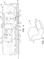
- Fig. 4 is a schematic sectional view of an optical module 60, in accordance with another embodiment of the invention.
- transmission lens assembly 30 is contained in a dual barrel, including an inner barrel 62 in which lenses 32 are mounted and an outer barrel 64, which is fixed to substrate 26.
- Outer barrel 64 includes a baffle 65, which protrudes asymmetrically toward substrate 26, between transmitter 21 and receiver 23.
- baffle 65 has an aperture that is configured to pass a small fraction of the radiation output by emitter 22 through the baffle toward optical sensor 24.
- a light guide 66 extends through baffle 65 order to control and direct the stray radiation from emitter 22 toward sensor 24.
- Light guide 66 is designed to pass a predefined fraction of the emitted optical radiation through the baffle and direct it toward the optical sensor.
- baffle 65 may simply contain an aperture for such stray light, without the light guide.
- Fig. 5 is a schematic pictorial view of light guide 66, in accordance with an embodiment of the invention.
- Light guide 66 comprises a suitable transparent material, such as a glass or transparent plastic.
- An entrance face 68 of the light guide is angled in this example to receive stray radiation that is reflected from lower lens 32 in transmission lens assembly 30.
- An exit face 70 of the light guide outputs the stray light toward sensor 24. Entrance face 68 and/or exit face 70 may be masked and/or coated in order to control the amount of radiation that is passes through the light guide.
- light guide 66 itself may comprise a volume of material that absorbs radiation for this purpose.
- light guide 66 may be shaped or patterned to control the spatial distribution of the stray radiation that is emitted through exit face 70.
- light guide 66 may be configured to direct the radiation specifically toward certain reference pixels in sensor, while avoiding irradiation of the pixels that receive radiation from the target.
- exit face 70 may be cylindrical or wedged, or may be patterned with a nano-structured diffractive optical element to control the direction of the light.
- the stray light transmitted through light guide 66 may be diffused by roughening exit face 70 or adding a lenslet array on the exit face.
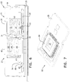
- Fig. 6 is a schematic sectional view of an optical module 80, in accordance with yet another embodiment of the invention.
- optical receiver 23 comprises a sensing assembly 82, which includes a submount 86, on which optical sensor 24 (not shown in this figure) is installed.
- An optical baffle 84 comprising a compressible radiation-absorbing material, such as a suitable closed-cell foam, surrounds the optical sensor.
- This compressible baffle 84 may be used instead of or in conjunction with a baffle on barrel 34 of transmission lens assembly 30, such as the asymmetrical barrels described above.
- optical transmitter 21 may comprise a compressible baffle of this sort.
- barrel 46 of objective lens assembly 42 presses against and compresses baffle 84, thus shutting out stray light from emitter 22.
- barrel 46 and baffle 84 may be designed to permit a small, controlled amount of stray light to reach sensor 24 for ToF calibration purposes.
- the use of such a compressible material in baffle 84 is also helpful in relaxing the manufacturing tolerances of module 80 and in absorbing mechanical shocks to sensing assembly 82 from objective lens assembly 42.
- Fig. 7 is a schematic pictorial view of a sensing assembly 90 with compressible baffle 84, in accordance with another embodiment of the invention.
- baffle comprises a compressible, radiation-absorbing foam disposed as a gasket around sensor 24 on the upper side of the chip package containing the sensor.
- Other configurations of this sort of compressible baffle will be apparent to those skilled in the art after reading the above description and are considered to be within the scope of the present invention.
Landscapes
- Physics & Mathematics (AREA)
- Engineering & Computer Science (AREA)
- General Physics & Mathematics (AREA)
- Computer Networks & Wireless Communication (AREA)
- Radar, Positioning & Navigation (AREA)
- Remote Sensing (AREA)
- Electromagnetism (AREA)
- Optics & Photonics (AREA)
- Optical Radar Systems And Details Thereof (AREA)
Abstract
Description
- The present invention relates generally to devices and methods for optical sensing, and particularly to optical transmitter/receiver modules.
- Some types of optical sensing systems include an optical transmitter, which transmits a beam of optical radiation toward a target, and an optical receiver, which collects and senses the optical radiation that is reflected from the target. (The term "optical radiation," in the context of the present description and in the claims, refers to electromagnetic radiation in any of the visible, infrared, and ultraviolet spectral ranges, and may be used interchangeably with the term "light.") For example, in some depth sensing systems, the transmitter emits pulses of radiation toward a target, and the optical receiver senses the times of flight (ToF) of the pulses, and thus measures the distance to the target.
- For many sensing applications, including ToF-based depth sensing, it can be advantageous to package the transmitter and receiver together on the same substrate in a compact package. An integrated optoelectronic module of this sort is described, for example, in
U.S. Patent 9,157,790 - ToF-based depth sensing devices are almost inevitably subject to stray reflections, which reflect or otherwise scatter from optical surfaces within the device back toward the receiver. In general, such stray reflections are regarded as noise, and designers of the devices do their best to eliminate them. On the other hand,
U.S. Patent 9,335,220 - Embodiments of the present invention that are described hereinbelow provide improved devices for optical transmission and reception.
- There is therefore provided, in accordance with an embodiment of the invention, an optical device, including a substrate and an optical transmitter, which is mounted on the substrate and includes an optical emitter, which is configured to emit a beam of optical radiation, and a transmission lens assembly, which is configured to direct the beam along a transmit axis toward a target. An optical receiver is mounted on the substrate alongside the optical transmitter and includes an optical sensor and an objective lens assembly, which is configured to focus the optical radiation that is reflected from the target along a receive axis onto the optical sensor. An optical baffle is disposed asymmetrically relative to the transmit axis and has an asymmetrical shape configured to block preferentially stray radiation emitted from the optical transmitter toward the receive axis.
- In some embodiments, the substrate includes an electrical circuit substrate on which the optical emitter and the optical sensor are mounted, and the device includes ancillary electronic components, which are mounted on the electrical circuit substrate and connected to the optical emitter and the optical sensor by electrical circuit traces. In a disclosed embodiment, the device includes a case, which contains the transmission lens assembly and the objective lens assembly and is fixed to the substrate so that the transmission lens assembly and the objective lens assembly are positioned respectively over the optical emitter and the optical sensor.
- In some embodiments, the transmission lens assembly includes one or more lenses mounted in a lens barrel, and the optical baffle protrudes asymmetrically from the lens barrel toward the substrate in a location between the transmit axis and the receive axis. In one embodiment, the optical baffle is an integral part of the lens barrel. Alternatively, the optical baffle includes a collar mounted on the lens barrel. Additionally or alternatively, the optical baffle includes an aperture configured to pass a predefined fraction of the emitted beam through the baffle toward the optical sensor.
- In a disclosed embodiment, the device includes a light guide extending through the baffle and configured to pass a predefined fraction of the emitted optical radiation through the baffle toward the optical sensor.
- In another embodiment, the optical baffle includes a compressible radiation-absorbing material, which is compressed upon assembly of the device, thereby preventing the stray radiation from reaching the optical sensor.
- There is also provided, in accordance with an embodiment of the invention, an optical device, including a substrate. An optical receiver, which is mounted on the substrate, includes an optical sensor and a compressible radiation-absorbing material surrounding the optical sensor. An objective lens assembly includes one or more lenses configured to focus optical radiation along a receive axis onto the optical sensor, and a lens barrel, which contains the one or more lenses, and which is mounted in the device so as to compress the radiation -absorbing material, thereby preventing stray radiation from reaching the optical sensor.
- In a disclosed embodiment, the device includes an optical transmitter, which is mounted on the substrate alongside the optical receiver, and which is configured to emit a beam of the optical radiation along a transmit axis toward a target, wherein the one or more lenses are configured to focus the optical radiation that is reflected from the target onto the optical sensor.
- Additionally or alternatively, the substrate includes an electrical circuit substrate on which the optical emitter and the optical sensor are mounted, and the device includes ancillary electronic components, which are mounted on the electrical circuit substrate and connected to the optical emitter and the optical sensor by electrical circuit traces.
- There is additionally provided, in accordance with an embodiment of the invention, a method for optical sensing, which includes mounting an optical transmitter on a substrate. The optical transmitter includes an optical emitter, which is configured to emit a beam of optical radiation, and a transmission lens assembly, which is configured to direct the beam along a transmit axis toward a target. An optical receiver is mounted on the substrate alongside the optical transmitter. The optical receiver includes an optical sensor and an objective lens assembly, which is configured to focus the optical radiation that is reflected from the target along a receive axis onto the optical sensor. An optical baffle is positioned asymmetrically relative to the transmit axis. The optical baffle has an asymmetrical shape configured to block preferentially stray radiation emitted from the optical transmitter toward the receive axis.
- The present invention will be more fully understood from the following detailed description of the embodiments thereof, taken together with the drawings in which:
-
-
Fig. 1 is a schematic sectional view of an optical module, in accordance with an embodiment of the invention; -
Fig. 2 is a schematic pictorial view of a transmission lens assembly, in accordance with an embodiment of the invention; -
Fig. 3A is a schematic pictorial view of a stray light baffle, in accordance with an embodiment of the invention; -
Fig. 3B is a schematic pictorial view of a transmission lens assembly incorporating the stray light baffle ofFig. 3A in an optical module, in accordance with an embodiment of the invention; -
Fig. 4 is a schematic sectional view of an optical module, in accordance with another embodiment of the invention; -
Fig. 5 is a schematic pictorial view of a light guide used in the optical module ofFig. 4 , in accordance with an embodiment of the invention; -
Fig. 6 is a schematic sectional view of an optical module, in accordance with yet another embodiment of the invention; and -
Fig. 7 is a schematic pictorial view of a sensing assembly with a compressible baffle, in accordance with an embodiment of the invention. - In designing an optical module that includes a transmitter and a receiver, it is important to minimize the amount of stray radiation that reaches the receiver, and particularly stray radiation emitted from the transmitter toward the receiver. This radiation is "stray" in the sense that it does not exit the module along the intended transmit path toward the target and then return from there to the receiver through the objective lens assembly, but rather reflects internally with the module, typically from one or more of the optical or mechanical surfaces in the module. Even a small amount of this sort of stray radiation can severely degrade the performance of the optical module, by adding substantial noise to the signals output by the receiver.
- Baffles are mechanical elements that are introduced into optical designs in order to block stray radiation and prevent it from reaching the target of the objective lens assembly (such as the sensor in a ToF sensing device). Baffles are usually designed to be a part of or attached to the barrel (i.e. the housing) of the objective lens assembly, with circular symmetry around the optical axis of the lens assembly.
- Careful optical design and baffling can eliminate most stray reflections; but when the transmitter and receiver are mounted together on the same substrate in a compact package, it is generally not possible to close off all possible paths that stray radiation could follow. For example, when ancillary electronic components are mounted on the substrate together with the optical emitter and the optical sensor, it may not be possible to surround the emitter or the sensor completely with a baffle that extends all the way down to the substrate. Furthermore, in ToF sensing modules, it may actually be desirable to allow a small amount of stray radiation to reach the optical sensor from the emitter in order to serve as a zero-reference for the ToF measurements, for example as described in the above-mentioned
U.S. Patent 9,335,220 - Some embodiments of the present invention address these problems using an asymmetrical stray light baffle. In these embodiments, an optical device comprises an optical transmitter and an optical receiver, both mounted on a substrate, one alongside the other. The optical transmitter comprises an optical emitter, which emits a beam of optical radiation (a pulsed beam in the case of ToF measurement), and a transmission lens assembly, which directs the beam along a transmit axis toward a target. The optical receiver comprises an optical sensor and an objective lens assembly, which focuses the optical radiation that is reflected from the target along a receive axis onto the optical sensor. An optical baffle is disposed asymmetrically relative to the transmit axis and has an asymmetrical shape that is designed to preferentially block stray radiation emitted from the optical transmitter from propagating toward the receive axis.
- In some of the present embodiments, the optical baffle protrudes asymmetrically from the lens barrel toward the substrate in a location between the transmit axis and the receive axis. This optical baffle may be an integral part of the lens barrel, or it may be a separate piece, for example in the form of a collar mounted on the lens barrel. In either case, the asymmetrical design makes it possible to mount ancillary electronic components on the substrate in close proximity to the emitter, typically on the side of the emitter opposite to the protruding baffle (i.e., on the opposite side from the receiver). The baffle can also be designed to permit a small, controlled amount of stray light to reach the optical sensor in order to serve as the zero reference. In one embodiment, the optical baffle comprises an aperture configured to pass a certain fraction of the emitted beam through the baffle toward the optical sensor.
- Reference is now made to
Figs. 1 and 2 , which schematically illustrate an optical device in the form of anoptical module 20, in accordance with an embodiment of the invention.Fig. 1 is a sectional view of the optical module, whileFig. 2 shows a pictorial view of atransmission lens assembly 30 inmodule 20. -
Module 20 comprises anoptical transmitter 21 and anoptical receiver 23, which are mounted one alongside the other on asubstrate 26.Substrate 26 typically comprises an electrical circuit substrate, such as a printed circuit board.Transmitter 21 comprises anoptical emitter 22, for example a suitable light-emitting diode (LED) or laser, such as a vertical-cavity surface-emitting laser (VCSEL), or an array of such LEDs or lasers, which may emit pulsed, continuous, or modulated radiation.Receiver 23 comprises anoptical sensor 24, for example an avalanche photodiode (APD) or a single-photon avalanche diode (SPAD) or an array of such photon detectors, or alternatively a detector or detector array that is capable of continuous or gated sensing.Emitter 22 andsensor 24 are mounted onsubstrate 26 together with ancillaryelectronic components 28, such as drivers, amplifiers and control circuits, which are typically connected to the emitter and the sensor by electrical circuit traces. -
Emitter 22 emits a beam of optical radiation, and atransmission lens assembly 30 collects and directs the beam along a transmitaxis 31 toward a target (not shown in the figures).Transmission lens assembly 30 comprises one or more lenses 32 (multiple lenses in the pictured example), which are mounted in alens barrel 34.Lenses 32 direct the beam through anexit window 36, which opens through acase 38. -
Receiver 23 comprises anobjective lens assembly 42, comprising one ormore lenses 44, which are mounted in abarrel 46.Lenses 44 focus the optical radiation that is reflected from the target along a receiveaxis 45 through anentrance window 40 incase 38 ontooptical sensor 24.Case 38 is fixed tosubstrate 26 so thattransmission lens assembly 30 andobjective lens assembly 42 are positioned respectively overoptical emitter 22 andoptical sensor 44. - An
optical baffle 48 protrudes asymmetrically fromlens barrel 34 towardsubstrate 26 in a location between transmitaxis 31 and receiveaxis 45. The asymmetrical shape and disposition ofbaffle 48 relative to transmitaxis 31 will preferentially block stray radiation emitted fromemitter 22 toward receive axis 45 (including both rays emitted directly from the emitter itself and rays reflected from other elements oftransmitter 21, such as from the surfaces of lenses 32). In this embodiment,optical baffle 48 is an integral part oflens barrel 34; but alternatively, the baffle may be produced separately and fastened to the lens barrel or otherwise mounted withincase 38. All such alternative implementations of an asymmetrical baffle of this sort are considered to be within the scope of the present invention. - The asymmetrical design of
optical baffle 48 has a number of advantages in the context ofmodule 20. This design can relieve other packaging constraints, for example by making it possible to mount relatively large ancillary components, such ascomponent 28 to the right ofemitter 22 inFig. 1 , in close proximity to the emitter. Furthermore, the baffle can be designed to permit a small amount of stray light to reachsensor 24, in order to enable ToF calibration without causing excessive noise inreceiver 23. - Reference is now made to
Figs. 3A and 3B , which schematically illustrate the design and operation of a straylight baffle 50, in accordance with another embodiment of the invention.Fig. 3A is a pictorial view ofbaffle 50, whileFig. 3B is a pictorial view oftransmission lens assembly 30 incorporatingbaffle 50 insidecase 38 of an optical module. -
Baffle 50 in this embodiment comprises acollar 52, which mounts onlens barrel 34. Anasymmetrical protrusion 54 extends abovecollar 52 in the area between transmitaxis 31 and receiveaxis 45, and thus preferentially blocks stray radiation emitted from the optical transmitter toward the receive axis. The use of this sort of separate collar component allows for greater flexibility of design and possibly easier assembly of the module. For example, the shape ofbaffle 50 can readily be molded as a separate component, but might be difficult to mold as an integral component of the lens barrel or might interfere with subsequent assembly oflenses 32 into the barrel. The use of a separate baffle of this sort also makes it possible to update and improve the baffle design without having to modify the entire lens barrel. -
Fig. 4 is a schematic sectional view of anoptical module 60, in accordance with another embodiment of the invention. In this embodiment,transmission lens assembly 30 is contained in a dual barrel, including aninner barrel 62 in whichlenses 32 are mounted and anouter barrel 64, which is fixed tosubstrate 26.Outer barrel 64 includes abaffle 65, which protrudes asymmetrically towardsubstrate 26, betweentransmitter 21 andreceiver 23. In this case, however, baffle 65 has an aperture that is configured to pass a small fraction of the radiation output byemitter 22 through the baffle towardoptical sensor 24. - In the pictured embodiment, a
light guide 66 extends throughbaffle 65 order to control and direct the stray radiation fromemitter 22 towardsensor 24.Light guide 66 is designed to pass a predefined fraction of the emitted optical radiation through the baffle and direct it toward the optical sensor. Alternatively, baffle 65 may simply contain an aperture for such stray light, without the light guide. -
Fig. 5 is a schematic pictorial view oflight guide 66, in accordance with an embodiment of the invention.Light guide 66 comprises a suitable transparent material, such as a glass or transparent plastic. An entrance face 68 of the light guide is angled in this example to receive stray radiation that is reflected fromlower lens 32 intransmission lens assembly 30. An exit face 70 of the light guide outputs the stray light towardsensor 24.Entrance face 68 and/orexit face 70 may be masked and/or coated in order to control the amount of radiation that is passes through the light guide. Additionally or alternatively,light guide 66 itself may comprise a volume of material that absorbs radiation for this purpose. - Further additionally or alternatively,
light guide 66 may be shaped or patterned to control the spatial distribution of the stray radiation that is emitted throughexit face 70. For example,light guide 66 may be configured to direct the radiation specifically toward certain reference pixels in sensor, while avoiding irradiation of the pixels that receive radiation from the target. For such purposes,exit face 70 may be cylindrical or wedged, or may be patterned with a nano-structured diffractive optical element to control the direction of the light. Alternatively, the stray light transmitted throughlight guide 66 may be diffused by rougheningexit face 70 or adding a lenslet array on the exit face. -
Fig. 6 is a schematic sectional view of anoptical module 80, in accordance with yet another embodiment of the invention. In this embodiment,optical receiver 23 comprises asensing assembly 82, which includes asubmount 86, on which optical sensor 24 (not shown in this figure) is installed. Anoptical baffle 84 comprising a compressible radiation-absorbing material, such as a suitable closed-cell foam, surrounds the optical sensor. Thiscompressible baffle 84 may be used instead of or in conjunction with a baffle onbarrel 34 oftransmission lens assembly 30, such as the asymmetrical barrels described above. Alternatively or additionally,optical transmitter 21 may comprise a compressible baffle of this sort. - When
module 80 is assembled,barrel 46 ofobjective lens assembly 42 presses against and compresses baffle 84, thus shutting out stray light fromemitter 22. Alternatively,barrel 46 and baffle 84 may be designed to permit a small, controlled amount of stray light to reachsensor 24 for ToF calibration purposes. The use of such a compressible material inbaffle 84 is also helpful in relaxing the manufacturing tolerances ofmodule 80 and in absorbing mechanical shocks to sensingassembly 82 fromobjective lens assembly 42. -
Fig. 7 is a schematic pictorial view of asensing assembly 90 withcompressible baffle 84, in accordance with another embodiment of the invention. In this example, baffle comprises a compressible, radiation-absorbing foam disposed as a gasket aroundsensor 24 on the upper side of the chip package containing the sensor. Other configurations of this sort of compressible baffle will be apparent to those skilled in the art after reading the above description and are considered to be within the scope of the present invention. - It will thus be appreciated that the embodiments described above are cited by way of example, and that the present invention is not limited to what has been particularly shown and described hereinabove. Rather, the scope of the present invention includes both combinations and subcombinations of the various features described hereinabove, as well as variations and modifications thereof which would occur to persons skilled in the art upon reading the foregoing description and which are not disclosed in the prior art.
Claims (15)
- An optical device (20, 60, 80), comprising:a substrate (26);an optical transmitter (21), which is mounted on the substrate and comprises an optical emitter (22), which is configured to emit a beam of optical radiation, and a transmission lens assembly (30), which is configured to direct the beam along a transmit axis (31) toward a target;an optical receiver (23), which is mounted on the substrate alongside the optical transmitter and comprises an optical sensor (24) and an objective lens assembly (42), which is configured to focus the optical radiation that is reflected from the target along a receive axis (45) onto the optical sensor; andan optical baffle (48, 50, 65) disposed asymmetrically relative to the transmit axis and having an asymmetrical shape configured to block preferentially stray radiation emitted from the optical transmitter toward the receive axis.
- The device according to claim 1, wherein the substrate comprises an electrical circuit substrate on which the optical emitter and the optical sensor are mounted, and the device comprises ancillary electronic components, which are mounted on the electrical circuit substrate and connected to the optical emitter and the optical sensor by electrical circuit traces.
- The device according to claim 2, and comprising a case, which contains the transmission lens assembly and the objective lens assembly and is fixed to the substrate so that the transmission lens assembly and the objective lens assembly are positioned respectively over the optical emitter and the optical sensor.
- The device according to any of claims 1-3, wherein the transmission lens assembly comprises one or more lenses mounted in a lens barrel, and the optical baffle protrudes asymmetrically from the lens barrel toward the substrate in a location between the transmit axis and the receive axis.
- The device according to claim 4, wherein the optical baffle is an integral part of the lens barrel.
- The device according to claim 4, wherein the optical baffle comprises a collar mounted on the lens barrel.
- The device according to claim 4, wherein the optical baffle comprises an aperture configured to pass a predefined fraction of the emitted beam through the baffle toward the optical sensor.
- The device according to any of claims 1-3, and comprising a light guide extending through the baffle and configured to pass a predefined fraction of the emitted optical radiation through the baffle toward the optical sensor.
- The device according to any of claims 1-3, wherein the optical baffle comprises a compressible radiation-absorbing material, which is compressed upon assembly of the device, thereby preventing the stray radiation from reaching the optical sensor.
- A method for optical sensing, comprising:mounting an optical transmitter (21) on a substrate (26), the optical transmitter comprising an optical emitter (22), which is configured to emit a beam of optical radiation, and a transmission lens assembly (30), which is configured to direct the beam along a transmit axis (31) toward a target;mounting an optical receiver (23) on the substrate alongside the optical transmitter, the optical receiver comprising an optical sensor (24) and an objective lens assembly (42), which is configured to focus the optical radiation that is reflected from the target along a receive axis (45) onto the optical sensor; andpositioning an optical baffle (48, 50, 65) asymmetrically relative to the transmit axis, the optical baffle having an asymmetrical shape configured to block preferentially stray radiation emitted from the optical transmitter toward the receive axis.
- The method according to claim 10, wherein the substrate comprises an electrical circuit substrate on which the optical emitter and the optical sensor are mounted, and the method comprises mounting ancillary electronic components on the electrical circuit substrate for connection to the optical emitter and the optical sensor by electrical circuit traces.
- The method according to claim 10 or 11, wherein the transmission lens assembly comprises one or more lenses mounted in a lens barrel, and the optical baffle protrudes asymmetrically from the lens barrel toward the substrate in a location between the transmit axis and the receive axis.
- The method according to claim 12, wherein the optical baffle is an integral part of the lens barrel.
- The method according to claim 12, wherein positioning the optical baffle comprises mounting a collar comprising the optical on the lens barrel.
- The method according to claim 10 or 11, wherein the optical baffle comprises a compressible radiation-absorbing material.
Applications Claiming Priority (1)
| Application Number | Priority Date | Filing Date | Title |
|---|---|---|---|
| US16/574,129 US11681019B2 (en) | 2019-09-18 | 2019-09-18 | Optical module with stray light baffle |
Publications (2)
| Publication Number | Publication Date |
|---|---|
| EP3796033A1 true EP3796033A1 (en) | 2021-03-24 |
| EP3796033B1 EP3796033B1 (en) | 2025-08-27 |
Family
ID=71170450
Family Applications (1)
| Application Number | Title | Priority Date | Filing Date |
|---|---|---|---|
| EP20182518.9A Active EP3796033B1 (en) | 2019-09-18 | 2020-06-26 | Optical module with stray light baffle |
Country Status (3)
| Country | Link |
|---|---|
| US (1) | US11681019B2 (en) |
| EP (1) | EP3796033B1 (en) |
| CN (1) | CN112526479B (en) |
Cited By (1)
| Publication number | Priority date | Publication date | Assignee | Title |
|---|---|---|---|---|
| EP4220239B1 (en) * | 2022-01-21 | 2024-12-25 | Leuze electronic GmbH + Co. KG | Optical sensor |
Families Citing this family (13)
| Publication number | Priority date | Publication date | Assignee | Title |
|---|---|---|---|---|
| CA3195228A1 (en) | 2020-09-18 | 2022-03-24 | Nubis Communications Inc. | Data processing systems including optical communication modules |
| US11988874B2 (en) | 2020-10-07 | 2024-05-21 | Nubis Communications, Inc. | Data processing systems including optical communication modules |
| TW202238198A (en) | 2020-11-20 | 2022-10-01 | 美商紐比斯通訊股份有限公司 | Thermal design for rack mount systems including optical communication modules |
| US12066653B2 (en) | 2021-04-22 | 2024-08-20 | Nubis Communications, Inc. | Communication systems having optical power supplies |
| US12461322B2 (en) | 2021-06-17 | 2025-11-04 | Nubis Communications, Inc. | Communication systems having pluggable modules |
| US12405433B2 (en) | 2021-06-17 | 2025-09-02 | Nubis Communications, Inc. | Communication systems having pluggable modules |
| EP4152065A1 (en) | 2021-09-16 | 2023-03-22 | Nubis Communications, Inc. | Communication systems having co-packaged optical modules |
| US12250024B2 (en) | 2021-09-16 | 2025-03-11 | Nubis Communications, Inc. | Data processing systems including optical communication modules |
| TW202345538A (en) * | 2022-01-11 | 2023-11-16 | 美商爾雅實驗室公司 | Systems and methods for remote optical power supply communication for uncooled wdm optical links |
| WO2023215315A1 (en) | 2022-05-02 | 2023-11-09 | Nubis Communications, Inc. | Communication systems having pluggable optical modules |
| US12270948B2 (en) * | 2022-08-05 | 2025-04-08 | Meta Platforms Technologies, Llc | Source-camera assembly with light path for a reference pixel |
| WO2024152017A1 (en) * | 2023-01-14 | 2024-07-18 | Leupold & Stevens, Inc. | Folded light path optic housing with integrally formed channel sections |
| CN121773349A (en) | 2023-09-11 | 2026-03-31 | 苹果公司 | Optical module |
Citations (4)
| Publication number | Priority date | Publication date | Assignee | Title |
|---|---|---|---|---|
| US20140218715A1 (en) * | 2013-02-05 | 2014-08-07 | Nen-Tsua Li | Structure of an optical path for laser range finding |
| US9157790B2 (en) | 2012-02-15 | 2015-10-13 | Apple Inc. | Integrated optoelectronic modules with transmitter, receiver and beam-combining optics for aligning a beam axis with a collection axis |
| US20160003944A1 (en) * | 2014-07-02 | 2016-01-07 | Robert Bosch Gmbh | Distance Measuring Device |
| US9335220B2 (en) | 2012-03-22 | 2016-05-10 | Apple Inc. | Calibration of time-of-flight measurement using stray reflections |
Family Cites Families (88)
| Publication number | Priority date | Publication date | Assignee | Title |
|---|---|---|---|---|
| GB1353470A (en) | 1970-10-19 | 1974-05-15 | Post D | Position measuring apparatus utilizing moire fringe multiplication |
| US4850673A (en) | 1987-11-23 | 1989-07-25 | U. S. Philips Corporation | Optical scanning apparatus which detects scanning spot focus error |
| EP0452793B1 (en) | 1990-04-12 | 1998-01-28 | Matsushita Electric Industrial Co., Ltd. | Optical head having a hologram associated with the objective lens |
| US5691989A (en) | 1991-07-26 | 1997-11-25 | Accuwave Corporation | Wavelength stabilized laser sources using feedback from volume holograms |
| US5477383A (en) | 1993-02-05 | 1995-12-19 | Apa Optics, Inc. | Optical array method and apparatus |
| US5406543A (en) | 1993-04-07 | 1995-04-11 | Olympus Optical Co., Ltd. | Optical head with semiconductor laser |
| JP3623250B2 (en) | 1993-06-23 | 2005-02-23 | オリンパス株式会社 | Video display device |
| JP3537881B2 (en) | 1994-03-29 | 2004-06-14 | 株式会社リコー | LED array head |
| JP2768320B2 (en) | 1995-09-04 | 1998-06-25 | 日本電気株式会社 | Tunable optical filter |
| JPH10227857A (en) | 1997-02-14 | 1998-08-25 | Nikon Corp | Lightwave ranging device |
| US6002520A (en) | 1997-04-25 | 1999-12-14 | Hewlett-Packard Company | Illumination system for creating a desired irradiance profile using diffractive optical elements |
| US6031611A (en) | 1997-06-03 | 2000-02-29 | California Institute Of Technology | Coherent gradient sensing method and system for measuring surface curvature |
| JPH11112097A (en) | 1997-09-30 | 1999-04-23 | Fujitsu Ltd | Light source module and optical scanning device |
| US6560019B2 (en) | 1998-02-05 | 2003-05-06 | Canon Kabushiki Kaisha | Diffractive optical element and optical system having the same |
| JP3940806B2 (en) | 1998-05-15 | 2007-07-04 | 株式会社ニコン | Lightwave ranging device |
| US6636538B1 (en) | 1999-03-29 | 2003-10-21 | Cutting Edge Optronics, Inc. | Laser diode packaging |
| US7262765B2 (en) | 1999-08-05 | 2007-08-28 | Microvision, Inc. | Apparatuses and methods for utilizing non-ideal light sources |
| US6690467B1 (en) | 2000-05-05 | 2004-02-10 | Pe Corporation | Optical system and method for optically analyzing light from a sample |
| US6583873B1 (en) | 2000-09-25 | 2003-06-24 | The Carnegie Institution Of Washington | Optical devices having a wavelength-tunable dispersion assembly that has a volume dispersive diffraction grating |
| WO2002037410A1 (en) | 2000-11-06 | 2002-05-10 | Koninklijke Philips Electronics N.V. | Method of measuring the movement of an input device. |
| US6611000B2 (en) | 2001-03-14 | 2003-08-26 | Matsushita Electric Industrial Co., Ltd. | Lighting device |
| WO2002089221A1 (en) | 2001-04-23 | 2002-11-07 | Matsushita Electric Works, Ltd. | Light emitting device comprising led chip |
| CN100338434C (en) | 2003-02-06 | 2007-09-19 | 株式会社高永科技 | Thrre-dimensional image measuring apparatus |
| US6940583B2 (en) | 2003-07-28 | 2005-09-06 | International Business Machines Corporation | Method and apparatus for amplitude filtering in the frequency plane of a lithographic projection system |
| US7112774B2 (en) | 2003-10-09 | 2006-09-26 | Avago Technologies Sensor Ip (Singapore) Pte. Ltd | CMOS stereo imaging system and method |
| US7053992B2 (en) | 2003-11-26 | 2006-05-30 | Meade Instruments Corporation | Rangefinder and method for collecting calibration data |
| US7961909B2 (en) | 2006-03-08 | 2011-06-14 | Electronic Scripting Products, Inc. | Computer interface employing a manipulated object with absolute pose detection component and a display |
| JP4535743B2 (en) | 2004-02-06 | 2010-09-01 | 株式会社東芝 | Optical scanning apparatus and image forming apparatus |
| JP2005236513A (en) | 2004-02-18 | 2005-09-02 | Fujinon Corp | Imaging apparatus |
| JP4572312B2 (en) | 2004-02-23 | 2010-11-04 | スタンレー電気株式会社 | LED and manufacturing method thereof |
| US7227618B1 (en) | 2004-03-24 | 2007-06-05 | Baokang Bi | Pattern generating systems |
| US7304735B2 (en) | 2004-04-02 | 2007-12-04 | Kla-Tencor Technologies | Broadband wavelength selective filter |
| CN101031837B (en) | 2004-07-23 | 2011-06-15 | 通用电气医疗集团尼亚加拉有限公司 | Method and apparatus for fluorescent confocal microscopy |
| JP4761751B2 (en) | 2004-10-06 | 2011-08-31 | 株式会社トプコン | Distance measuring device |
| JP5128047B2 (en) | 2004-10-07 | 2013-01-23 | Towa株式会社 | Optical device and optical device production method |
| IL165212A (en) | 2004-11-15 | 2012-05-31 | Elbit Systems Electro Optics Elop Ltd | Device for scanning light |
| WO2007043036A1 (en) | 2005-10-11 | 2007-04-19 | Prime Sense Ltd. | Method and system for object reconstruction |
| US7750356B2 (en) | 2005-05-04 | 2010-07-06 | Avago Technologies Fiber Ip (Singapore) Pte. Ltd. | Silicon optical package with 45 degree turning mirror |
| US7609875B2 (en) | 2005-05-27 | 2009-10-27 | Orametrix, Inc. | Scanner system and method for mapping surface of three-dimensional object |
| CN1725042B (en) | 2005-06-30 | 2010-11-24 | 昆明理工大学 | Scanning Grating Writing Method Based on Talbot Interferometer and Scanning Talbot Interferometer |
| US7583875B2 (en) | 2005-07-22 | 2009-09-01 | Seiko Epson Corporation | Illumination device, image display device, and projector |
| US8390821B2 (en) | 2005-10-11 | 2013-03-05 | Primesense Ltd. | Three-dimensional sensing using speckle patterns |
| WO2007105205A2 (en) | 2006-03-14 | 2007-09-20 | Prime Sense Ltd. | Three-dimensional sensing using speckle patterns |
| US8792978B2 (en) | 2010-05-28 | 2014-07-29 | Lockheed Martin Corporation | Laser-based nerve stimulators for, E.G., hearing restoration in cochlear prostheses and method |
| US8542421B2 (en) | 2006-11-17 | 2013-09-24 | Celloptic, Inc. | System, apparatus and method for extracting three-dimensional information of an object from received electromagnetic radiation |
| US7990545B2 (en) | 2006-12-27 | 2011-08-02 | Cambridge Research & Instrumentation, Inc. | Surface measurement of in-vivo subjects using spot projector |
| US20080212835A1 (en) | 2007-03-01 | 2008-09-04 | Amon Tavor | Object Tracking by 3-Dimensional Modeling |
| US8150142B2 (en) | 2007-04-02 | 2012-04-03 | Prime Sense Ltd. | Depth mapping using projected patterns |
| WO2008120217A2 (en) | 2007-04-02 | 2008-10-09 | Prime Sense Ltd. | Depth mapping using projected patterns |
| CA2684602A1 (en) | 2007-04-23 | 2008-11-06 | California Institute Of Technology | Single-lens, 3-d imaging device using polarization-coded aperture masks combined with a polarization-sensitive sensor |
| JP4412362B2 (en) | 2007-07-18 | 2010-02-10 | 船井電機株式会社 | Compound eye imaging device |
| KR101439434B1 (en) | 2007-10-05 | 2014-09-12 | 삼성전자주식회사 | Image sensor and manufacturing method thereof |
| CN101874221B (en) | 2007-11-28 | 2012-06-13 | 日本电气株式会社 | Optical scanning device and image outputting device |
| US8166421B2 (en) | 2008-01-14 | 2012-04-24 | Primesense Ltd. | Three-dimensional user interface |
| EP2235584B1 (en) | 2008-01-21 | 2020-09-16 | Apple Inc. | Optical designs for zero order reduction |
| US8384997B2 (en) | 2008-01-21 | 2013-02-26 | Primesense Ltd | Optical pattern projection |
| US8331006B2 (en) | 2008-02-13 | 2012-12-11 | Nokia Corporation | Display device and a method for illuminating a light modulator array of a display device |
| JP5120000B2 (en) | 2008-03-19 | 2013-01-16 | 船井電機株式会社 | Image display device |
| US8456517B2 (en) | 2008-07-09 | 2013-06-04 | Primesense Ltd. | Integrated processor for 3D mapping |
| US7786418B2 (en) * | 2008-11-21 | 2010-08-31 | Raytheon Company | Multimode seeker system with RF transparent stray light baffles |
| CN101452076B (en) * | 2008-12-30 | 2011-12-14 | 中国科学院安徽光学精密机械研究所 | Optical-mechanical system of semiconductor laser cloud height automatic measuring instrument |
| CN201378231Y (en) | 2009-03-31 | 2010-01-06 | 北京北科天绘科技有限公司 | An optical scanning device |
| JP5588310B2 (en) | 2009-11-15 | 2014-09-10 | プライムセンス リミテッド | Optical projector with beam monitor |
| DE102009046911A1 (en) | 2009-11-20 | 2011-05-26 | Robert Bosch Gmbh | Method for recording image from surrounding field of vehicle, involves transmitting light pulses of pulse light source at equidistant angle values of tilting angle of micro mirror with respect to tilting direction |
| CN102087374A (en) * | 2009-12-02 | 2011-06-08 | 鸿富锦精密工业(深圳)有限公司 | Optical filter and lens module group using the same |
| JP5452197B2 (en) | 2009-12-03 | 2014-03-26 | パナソニック株式会社 | MEMS optical scanner |
| DE102009054592A1 (en) | 2009-12-14 | 2011-06-16 | Dr. Johannes Heidenhain Gmbh | Position measuring device |
| US20110187878A1 (en) | 2010-02-02 | 2011-08-04 | Primesense Ltd. | Synchronization of projected illumination with rolling shutter of image sensor |
| US20110188054A1 (en) | 2010-02-02 | 2011-08-04 | Primesense Ltd | Integrated photonics module for optical projection |
| US8279418B2 (en) | 2010-03-17 | 2012-10-02 | Microsoft Corporation | Raster scanning for depth detection |
| CN102200431B (en) | 2010-03-26 | 2013-10-02 | 德律科技股份有限公司 | A system for measuring three-dimensional objects |
| US9036158B2 (en) | 2010-08-11 | 2015-05-19 | Apple Inc. | Pattern projector |
| WO2012020380A1 (en) | 2010-08-11 | 2012-02-16 | Primesense Ltd. | Scanning projectors and image capture modules for 3d mapping |
| US8466407B2 (en) | 2010-10-07 | 2013-06-18 | Raytheon Company | Stray light baffles for a conformal dome with arch corrector optics |
| EP2643659B1 (en) | 2010-11-19 | 2019-12-25 | Apple Inc. | Depth mapping using time-coded illumination |
| US9167138B2 (en) | 2010-12-06 | 2015-10-20 | Apple Inc. | Pattern projection and imaging using lens arrays |
| US8908277B2 (en) | 2011-08-09 | 2014-12-09 | Apple Inc | Lens array projector |
| US8749796B2 (en) | 2011-08-09 | 2014-06-10 | Primesense Ltd. | Projectors of structured light |
| WO2013140308A1 (en) | 2012-03-22 | 2013-09-26 | Primesense Ltd. | Diffraction-based sensing of mirror position |
| CN103676420B (en) | 2012-09-04 | 2015-08-19 | 光宝科技股份有限公司 | Laser scanning projection device with phase detection and compensation functions |
| EP2926225A4 (en) | 2013-02-14 | 2016-07-27 | Apple Inc | Flexible room controls |
| KR101806753B1 (en) * | 2013-06-17 | 2017-12-07 | 애플 인크. | Modular optics for scanning engine |
| US9202833B2 (en) | 2013-08-23 | 2015-12-01 | Semiconductor Components Industries, Llc | Imaging systems with baffle grids |
| JP6053171B2 (en) | 2013-10-18 | 2016-12-27 | 増田 麻言 | Scanning projection apparatus and portable projection apparatus |
| CN204580451U (en) | 2015-02-04 | 2015-08-26 | 天津百圣利亨钢木家具有限公司 | Bookcase |
| US10012831B2 (en) | 2015-08-03 | 2018-07-03 | Apple Inc. | Optical monitoring of scan parameters |
| CN108663670B (en) * | 2018-05-15 | 2021-06-01 | 武汉万集信息技术有限公司 | Laser radar optical-mechanical device |
| US10950743B2 (en) | 2019-05-02 | 2021-03-16 | Stmicroelectronics (Research & Development) Limited | Time of flight (TOF) sensor with transmit optic providing for reduced parallax effect |
-
2019
- 2019-09-18 US US16/574,129 patent/US11681019B2/en active Active
-
2020
- 2020-06-26 EP EP20182518.9A patent/EP3796033B1/en active Active
- 2020-07-30 CN CN202010749774.XA patent/CN112526479B/en active Active
Patent Citations (4)
| Publication number | Priority date | Publication date | Assignee | Title |
|---|---|---|---|---|
| US9157790B2 (en) | 2012-02-15 | 2015-10-13 | Apple Inc. | Integrated optoelectronic modules with transmitter, receiver and beam-combining optics for aligning a beam axis with a collection axis |
| US9335220B2 (en) | 2012-03-22 | 2016-05-10 | Apple Inc. | Calibration of time-of-flight measurement using stray reflections |
| US20140218715A1 (en) * | 2013-02-05 | 2014-08-07 | Nen-Tsua Li | Structure of an optical path for laser range finding |
| US20160003944A1 (en) * | 2014-07-02 | 2016-01-07 | Robert Bosch Gmbh | Distance Measuring Device |
Cited By (1)
| Publication number | Priority date | Publication date | Assignee | Title |
|---|---|---|---|---|
| EP4220239B1 (en) * | 2022-01-21 | 2024-12-25 | Leuze electronic GmbH + Co. KG | Optical sensor |
Also Published As
| Publication number | Publication date |
|---|---|
| US20210080546A1 (en) | 2021-03-18 |
| CN112526479B (en) | 2024-06-25 |
| US11681019B2 (en) | 2023-06-20 |
| CN112526479A (en) | 2021-03-19 |
| EP3796033B1 (en) | 2025-08-27 |
Similar Documents
| Publication | Publication Date | Title |
|---|---|---|
| EP3796033B1 (en) | Optical module with stray light baffle | |
| EP1505421B1 (en) | Optical link device | |
| CN108663670B (en) | Laser radar optical-mechanical device | |
| CN105629213B (en) | Multi-sensor proximity sensing | |
| EP4086657B1 (en) | Laser transceiving module, lidar, and autonomous driving device | |
| KR20230126704A (en) | LiDAR system using transmit optical power monitor | |
| KR102549175B1 (en) | LIDAR measurement system with wavelength conversion | |
| US12411214B2 (en) | Limited reflection type sensor | |
| WO2016021384A1 (en) | Optical receptacle and optical module | |
| CN216083083U (en) | Coaxial optical system for laser ranging | |
| WO2021134689A1 (en) | Distance measuring apparatus and distance measuring system | |
| KR20220074519A (en) | An improved ToF Sensor Device | |
| CN223486191U (en) | Optical ranging sensor and electronic system configured to determine the proximity of a target object | |
| US9939530B2 (en) | Optical system for extended time of flight ranging | |
| KR101725797B1 (en) | Light projection head and optical sensor | |
| US10739537B2 (en) | Optical receptacle and optical module | |
| CN219122404U (en) | Receiving and transmitting device of laser radar | |
| US11506762B1 (en) | Optical module comprising an optical waveguide with reference light path | |
| US20050169644A1 (en) | Optical signal transmitting device | |
| CN212275965U (en) | Shading assembly | |
| US20250109983A1 (en) | Module packaging architecture to reduce crosstalk in an optical sensor | |
| WO2025016449A1 (en) | LIGHT DETECTOR CHIP, LIGHT EMITTER CHIP, AND LiDAR | |
| US20250137841A1 (en) | Optical sensor module | |
| CN224216869U (en) | A line laser ranging device and a robot | |
| KR100820004B1 (en) | Bidirectional Optical Signal Transceiver |
Legal Events
| Date | Code | Title | Description |
|---|---|---|---|
| PUAI | Public reference made under article 153(3) epc to a published international application that has entered the european phase |
Free format text: ORIGINAL CODE: 0009012 |
|
| STAA | Information on the status of an ep patent application or granted ep patent |
Free format text: STATUS: REQUEST FOR EXAMINATION WAS MADE |
|
| 17P | Request for examination filed |
Effective date: 20200626 |
|
| AK | Designated contracting states |
Kind code of ref document: A1 Designated state(s): AL AT BE BG CH CY CZ DE DK EE ES FI FR GB GR HR HU IE IS IT LI LT LU LV MC MK MT NL NO PL PT RO RS SE SI SK SM TR |
|
| AX | Request for extension of the european patent |
Extension state: BA ME |
|
| STAA | Information on the status of an ep patent application or granted ep patent |
Free format text: STATUS: EXAMINATION IS IN PROGRESS |
|
| 17Q | First examination report despatched |
Effective date: 20220920 |
|
| GRAP | Despatch of communication of intention to grant a patent |
Free format text: ORIGINAL CODE: EPIDOSNIGR1 |
|
| STAA | Information on the status of an ep patent application or granted ep patent |
Free format text: STATUS: GRANT OF PATENT IS INTENDED |
|
| RIC1 | Information provided on ipc code assigned before grant |
Ipc: G01S 7/497 20060101ALN20250313BHEP Ipc: G01S 17/10 20200101ALI20250313BHEP Ipc: G01S 7/481 20060101AFI20250313BHEP |
|
| INTG | Intention to grant announced |
Effective date: 20250324 |
|
| P01 | Opt-out of the competence of the unified patent court (upc) registered |
Free format text: CASE NUMBER: APP_28008/2025 Effective date: 20250611 |
|
| GRAS | Grant fee paid |
Free format text: ORIGINAL CODE: EPIDOSNIGR3 |
|
| GRAA | (expected) grant |
Free format text: ORIGINAL CODE: 0009210 |
|
| STAA | Information on the status of an ep patent application or granted ep patent |
Free format text: STATUS: THE PATENT HAS BEEN GRANTED |
|
| AK | Designated contracting states |
Kind code of ref document: B1 Designated state(s): AL AT BE BG CH CY CZ DE DK EE ES FI FR GB GR HR HU IE IS IT LI LT LU LV MC MK MT NL NO PL PT RO RS SE SI SK SM TR |
|
| REG | Reference to a national code |
Ref country code: GB Ref legal event code: FG4D |
|
| REG | Reference to a national code |
Ref country code: CH Ref legal event code: EP |
|
| REG | Reference to a national code |
Ref country code: DE Ref legal event code: R096 Ref document number: 602020057285 Country of ref document: DE |
|
| REG | Reference to a national code |
Ref country code: IE Ref legal event code: FG4D |
|
| REG | Reference to a national code |
Ref country code: NL Ref legal event code: MP Effective date: 20250827 |
|
| PG25 | Lapsed in a contracting state [announced via postgrant information from national office to epo] |
Ref country code: IS Free format text: LAPSE BECAUSE OF FAILURE TO SUBMIT A TRANSLATION OF THE DESCRIPTION OR TO PAY THE FEE WITHIN THE PRESCRIBED TIME-LIMIT Effective date: 20251227 |
|
| PG25 | Lapsed in a contracting state [announced via postgrant information from national office to epo] |
Ref country code: NO Free format text: LAPSE BECAUSE OF FAILURE TO SUBMIT A TRANSLATION OF THE DESCRIPTION OR TO PAY THE FEE WITHIN THE PRESCRIBED TIME-LIMIT Effective date: 20251127 |
|
| REG | Reference to a national code |
Ref country code: LT Ref legal event code: MG9D |
|
| PG25 | Lapsed in a contracting state [announced via postgrant information from national office to epo] |
Ref country code: PT Free format text: LAPSE BECAUSE OF FAILURE TO SUBMIT A TRANSLATION OF THE DESCRIPTION OR TO PAY THE FEE WITHIN THE PRESCRIBED TIME-LIMIT Effective date: 20251229 |
|
| PG25 | Lapsed in a contracting state [announced via postgrant information from national office to epo] |
Ref country code: FI Free format text: LAPSE BECAUSE OF FAILURE TO SUBMIT A TRANSLATION OF THE DESCRIPTION OR TO PAY THE FEE WITHIN THE PRESCRIBED TIME-LIMIT Effective date: 20250827 |
|
| PG25 | Lapsed in a contracting state [announced via postgrant information from national office to epo] |
Ref country code: HR Free format text: LAPSE BECAUSE OF FAILURE TO SUBMIT A TRANSLATION OF THE DESCRIPTION OR TO PAY THE FEE WITHIN THE PRESCRIBED TIME-LIMIT Effective date: 20250827 Ref country code: NL Free format text: LAPSE BECAUSE OF FAILURE TO SUBMIT A TRANSLATION OF THE DESCRIPTION OR TO PAY THE FEE WITHIN THE PRESCRIBED TIME-LIMIT Effective date: 20250827 |
|
| PG25 | Lapsed in a contracting state [announced via postgrant information from national office to epo] |
Ref country code: GR Free format text: LAPSE BECAUSE OF FAILURE TO SUBMIT A TRANSLATION OF THE DESCRIPTION OR TO PAY THE FEE WITHIN THE PRESCRIBED TIME-LIMIT Effective date: 20251128 |
|
| PG25 | Lapsed in a contracting state [announced via postgrant information from national office to epo] |
Ref country code: SE Free format text: LAPSE BECAUSE OF FAILURE TO SUBMIT A TRANSLATION OF THE DESCRIPTION OR TO PAY THE FEE WITHIN THE PRESCRIBED TIME-LIMIT Effective date: 20250827 |
|
| PG25 | Lapsed in a contracting state [announced via postgrant information from national office to epo] |
Ref country code: LV Free format text: LAPSE BECAUSE OF FAILURE TO SUBMIT A TRANSLATION OF THE DESCRIPTION OR TO PAY THE FEE WITHIN THE PRESCRIBED TIME-LIMIT Effective date: 20250827 |
|
| PG25 | Lapsed in a contracting state [announced via postgrant information from national office to epo] |
Ref country code: BG Free format text: LAPSE BECAUSE OF FAILURE TO SUBMIT A TRANSLATION OF THE DESCRIPTION OR TO PAY THE FEE WITHIN THE PRESCRIBED TIME-LIMIT Effective date: 20250827 Ref country code: PL Free format text: LAPSE BECAUSE OF FAILURE TO SUBMIT A TRANSLATION OF THE DESCRIPTION OR TO PAY THE FEE WITHIN THE PRESCRIBED TIME-LIMIT Effective date: 20250827 |
|
| PG25 | Lapsed in a contracting state [announced via postgrant information from national office to epo] |
Ref country code: RS Free format text: LAPSE BECAUSE OF FAILURE TO SUBMIT A TRANSLATION OF THE DESCRIPTION OR TO PAY THE FEE WITHIN THE PRESCRIBED TIME-LIMIT Effective date: 20251127 |
|
| PG25 | Lapsed in a contracting state [announced via postgrant information from national office to epo] |
Ref country code: ES Free format text: LAPSE BECAUSE OF FAILURE TO SUBMIT A TRANSLATION OF THE DESCRIPTION OR TO PAY THE FEE WITHIN THE PRESCRIBED TIME-LIMIT Effective date: 20250827 |
|
| REG | Reference to a national code |
Ref country code: AT Ref legal event code: MK05 Ref document number: 1830525 Country of ref document: AT Kind code of ref document: T Effective date: 20250827 |
|
| PG25 | Lapsed in a contracting state [announced via postgrant information from national office to epo] |
Ref country code: SM Free format text: LAPSE BECAUSE OF FAILURE TO SUBMIT A TRANSLATION OF THE DESCRIPTION OR TO PAY THE FEE WITHIN THE PRESCRIBED TIME-LIMIT Effective date: 20250827 |
|
| PG25 | Lapsed in a contracting state [announced via postgrant information from national office to epo] |
Ref country code: DK Free format text: LAPSE BECAUSE OF FAILURE TO SUBMIT A TRANSLATION OF THE DESCRIPTION OR TO PAY THE FEE WITHIN THE PRESCRIBED TIME-LIMIT Effective date: 20250827 |
|
| PG25 | Lapsed in a contracting state [announced via postgrant information from national office to epo] |
Ref country code: AT Free format text: LAPSE BECAUSE OF FAILURE TO SUBMIT A TRANSLATION OF THE DESCRIPTION OR TO PAY THE FEE WITHIN THE PRESCRIBED TIME-LIMIT Effective date: 20250827 |
|
| PG25 | Lapsed in a contracting state [announced via postgrant information from national office to epo] |
Ref country code: IT Free format text: LAPSE BECAUSE OF FAILURE TO SUBMIT A TRANSLATION OF THE DESCRIPTION OR TO PAY THE FEE WITHIN THE PRESCRIBED TIME-LIMIT Effective date: 20250827 |
|
| PG25 | Lapsed in a contracting state [announced via postgrant information from national office to epo] |
Ref country code: CZ Free format text: LAPSE BECAUSE OF FAILURE TO SUBMIT A TRANSLATION OF THE DESCRIPTION OR TO PAY THE FEE WITHIN THE PRESCRIBED TIME-LIMIT Effective date: 20250827 |
|
| PG25 | Lapsed in a contracting state [announced via postgrant information from national office to epo] |
Ref country code: EE Free format text: LAPSE BECAUSE OF FAILURE TO SUBMIT A TRANSLATION OF THE DESCRIPTION OR TO PAY THE FEE WITHIN THE PRESCRIBED TIME-LIMIT Effective date: 20250827 Ref country code: SK Free format text: LAPSE BECAUSE OF FAILURE TO SUBMIT A TRANSLATION OF THE DESCRIPTION OR TO PAY THE FEE WITHIN THE PRESCRIBED TIME-LIMIT Effective date: 20250827 |