EP3796013A1 - Interface adapted to receive a radio frequency probe for testing an electric device, and method for testing an electric device arranged on a substrate - Google Patents
Interface adapted to receive a radio frequency probe for testing an electric device, and method for testing an electric device arranged on a substrate Download PDFInfo
- Publication number
- EP3796013A1 EP3796013A1 EP19198097.8A EP19198097A EP3796013A1 EP 3796013 A1 EP3796013 A1 EP 3796013A1 EP 19198097 A EP19198097 A EP 19198097A EP 3796013 A1 EP3796013 A1 EP 3796013A1
- Authority
- EP
- European Patent Office
- Prior art keywords
- interface
- conductive structure
- probe
- capacitive element
- substrate
- Prior art date
- Legal status (The legal status is an assumption and is not a legal conclusion. Google has not performed a legal analysis and makes no representation as to the accuracy of the status listed.)
- Granted
Links
Images





Classifications
-
- G—PHYSICS
- G01—MEASURING; TESTING
- G01R—MEASURING ELECTRIC VARIABLES; MEASURING MAGNETIC VARIABLES
- G01R31/00—Arrangements for testing electric properties; Arrangements for locating electric faults; Arrangements for electrical testing characterised by what is being tested not provided for elsewhere
- G01R31/28—Testing of electronic circuits, e.g. by signal tracer
- G01R31/2851—Testing of integrated circuits [IC]
- G01R31/2884—Testing of integrated circuits [IC] using dedicated test connectors, test elements or test circuits on the IC under test
-
- G—PHYSICS
- G01—MEASURING; TESTING
- G01R—MEASURING ELECTRIC VARIABLES; MEASURING MAGNETIC VARIABLES
- G01R31/00—Arrangements for testing electric properties; Arrangements for locating electric faults; Arrangements for electrical testing characterised by what is being tested not provided for elsewhere
- G01R31/28—Testing of electronic circuits, e.g. by signal tracer
- G01R31/282—Testing of electronic circuits specially adapted for particular applications not provided for elsewhere
- G01R31/2822—Testing of electronic circuits specially adapted for particular applications not provided for elsewhere of microwave or radiofrequency circuits
Definitions
- Examples relate to testing electric devices using Radio Frequency (RF) probes.
- examples relate to an interface adapted to receive a RF probe for testing an electric device that is arranged on a same substrate as the interface. Further examples relate to a method for testing an electric device arranged on a substrate.
- RF Radio Frequency
- RF measurement of test devices on a system board requires so called launch structures (also known as launchers) for providing interconnection between RF probes and transmission lines on the board.
- launch structures also known as launchers
- a launcher should be broadband and "transparent" for the measured signals. In other words, it should not introduce signal losses and signal reflections at the interface of the RF probe and the board.
- An example relates to an interface adapted to receive a RF probe for testing an electric device that is arranged on a same substrate as the interface.
- the interface comprises a first conductive structure for receiving at least one probe tip of the RF probe.
- the first conductive structure is coupled to a signal line in or on the substrate that couples to the electric device.
- the interface comprises a second conductive structure for receiving at least one further probe tip of the RF probe.
- the interface additionally comprises a capacitive element for providing a compensation capacitance.
- the capacitive element and the first conductive structure are electrically coupled in order to form a compensation network for compensating RF parasitics.
- Another example relates to an electric system comprising an electric device arranged on a substrate, and an interface as described herein which is arranged on the substrate.
- a further example relates to a method for testing an electric device arranged on a substrate.
- the method comprises placing a RF probe onto an interface arranged on the substrate such that a first conductive structure of the interface receives at least one probe tip of the RF probe and that a second conductive structure of the interface receives at least one further probe tip of the RF probe.
- the first conductive structure is coupled to a signal line in or on the substrate that couples to the electric device.
- the first conductive structure and a capacitive element for providing a compensation capacitance are electrically coupled in order to form a compensation network for compensating RF parasitics.
- the method additionally comprises applying a test signal to the interface via the at least one probe tip.
- Fig. 1 illustrates an example of an interface 100 adapted to receive a RF probe (not illustrated) for testing an electric device (not illustrated) that is arranged on a same (test) substrate 199 as the interface 100.
- the substrate 199 serves as a substrate for the electric device and the interface 100.
- the substrate 199 may be a Printed Circuit Board (PCB) or a glass substrate.
- the electric device may be understood as a Device Under Test (DUT). It is to be noted that the electric device may be mounted on the substrate 199 or be embedded within the substrate 199.
- the RF probe may, e.g., be a Ground-Signal-Ground (GSG) probe for RF testing the electric device.
- GSG Ground-Signal-Ground
- the interface comprises a first conductive structure 110 for receiving at least one probe tip of the RF probe, and a second conductive structure 120 for receiving at least one further probe tip of the RF probe.
- the first conductive structure 110 and the second conductive structure 120 may be coplanar, i.e. be arranged in a same layer. Alternatively, the first conductive structure 110 and the second conductive structure 120 may be arranged in different layers.
- the first conductive structure 110 and the second conductive structure 120 may, e.g., be metal structures.
- the second conductive structure 120 is for receiving a reference signal from the at least one further probe tip of the RF probe (e.g. a ground reference from two further probe tips of the RF probe).
- the second conductive structure 120 electrically couples to the electric device by one or more vias of the substrate.
- the second conductive structure 120 electrically couples to four vias 101, 102, 103 and 104.
- the electric device may be coupled to a defined reference signal (e.g. a reference ground) while measuring/characterizing the electric device by means of the RF probe.
- the first conductive structure 110 is for receiving a test signal from the at least one probe tip of the RF probe.
- the at least one probe tip is used to apply a test signal to the interface 100 and, hence, the electric device. Therefore, the first conductive structure 110 is coupled at a first end 111 to a signal line 150 on the substrate 199 that couples to the electric device. In other words, the first conductive structure 110 is coupled to the electric device via the signal line 150.
- the signal line 150 is a conductive path routed on the substrate (e.g. the surface of the substrate).
- the signal line 150 may be a MicroStrip Line (MSL).
- GSG probe is merely an example for an RF probe.
- any type of RF probe may be used.
- an RF probe comprising only a probe tip for applying a test signal to the first conductive structure 110, and only one other probe tip for applying a reference signal to the second conductive structure 120 may be used.
- one or more additional signal lines e.g. coplanar to transmission line 150 may be used for coupling the second conductive structure 120 to the electric device instead of the vias illustrated in Fig. 1 .
- the first conductive structure 110 is for instance strip-shaped.
- strip-shaped is to be understood such that a dimension (extension) of an element such as first conductive structure 110 along a spatial axis is much greater (e.g. at least two, three, four, five, ten, twenty, fifty or one hundred times greater) than a dimension of the element along another spatial axis which is orthogonal to the spatial axis.
- the first conductive structure 110 extends lengthwise along a spatial axis x such that the dimension of the first conductive structure 110 along the spatial axis x is much greater than the dimension of the first conductive structure 110 along the other spatial axis y which is orthogonal to the spatial axis x .
- any conductive structure or material forming the signal path between the signal line 150 and the position at which the RF probe is placed on (touches) the first conductive structure 110 leads to a (small) series inductance L feed (see Fig. 2 ).
- part of the first conductive structure 110 as well as the short interconnection 170 between the first conductive structure 110 and the signal line 150 may cause the series inductance L feed in the example of Fig. 1 .
- the series inductance together with the capacitance C TL of the signal line 150 causes unwanted RF parasitics at the interface.
- RF parasitics become especially problematic when the dimensions of the interface 100 and/or the probe have an order of magnitude which is close or equal to that of the wavelength of the test signal (e.g. when they differ from two orders of magnitude or less or are of the same order of magnitude).
- the interface 100 further comprises a capacitive element 140 for providing a compensation capacitance C compensate .
- the capacitive element 140 and the first conductive structure 110 are electrically coupled in order to form a compensation network for compensating the RF parasitics.
- the capacitive element 140 is not in electrical contact with the second conductive structure 120 since the capacitive element 140 does not touch the second conductive structure 120.
- the capacitive element 140 electrically couples (is attached) to a second end 112 of the first conductive structure 110.
- the capacitive element 140 and the signal line 150 are arranged on opposite sides of each of the first conductive structure 110 along the spatial axis x . In other words, a compensation capacitance C compensate is added at the RF probe side of the structure illustrated in Fig. 1 .
- FIG. 2 An equivalent circuit of the example depicted in Fig. 1 is illustrated in Fig. 2 .
- the inherent capacitance of the signal line 150 is represented by the capacitance C TL .
- the capacitive element 140 adds a compensation capacitance C compensate such that the series inductance L feed and the compensation capacitance C compensate of the capacitive element 140 form an LC compensation network that allows to compensate at least in part for the unwanted RF parasitics caused by the series inductance L feed and the capacitance C TL of the signal line 150.
- the compensation capacitance C compensate of the capacitive element 140 may allow to compensate for the series inductance Lfeed.
- the compensation capacitance C com-pensate of the capacitive element 140 may allow for a significantly increased bandwidth of the interface 100 compared to conventional launcher structures.
- the proposed incorporation of an LC compensation network into the launcher structure may allow to compensate for RF probe-to-substrate transition related parasitics.
- the second conductive structure 120 is formed integrally such that end portions 121 and 122 of the second conductive structure 120 are arranged on opposite sides of the spatial axis x .
- the second conductive structure 120 defines an inner space 130 within which the capacitive element 140 is arranged. All or part of the first conductive structure 110 may also be arranged within the inner space 130.
- the shape of the second conductive structure 120 is symmetrical with respect to the spatial axis x . It is to be noted that the respective locations of the vias 101, ..., 104 need not be symmetrical with respect to the spatial axis x . In alternative examples, the shape of the second conductive structure 120 may be asymmetrical with respect to the spatial axis x .
- the capacitive element 140 may be implemented in many different ways.
- the capacitive element 140 may be implemented with a fixed, predetermined capacitance or with an adjustable capacitance (e.g. depending on the frequency of the test signal to be applied via the first conductive structure 110).
- the capacitive element 140 is a metal pad (patch) of a predefined capacitance (e.g. the desired compensation capacitance C compensate ).
- the capacitive element 140 may alternatively be formed by any other suitable electrically conductive material such as electrically conductive ceramics.
- the metal pad is irregularly shaped.
- the capacitive element 140 may, in general, be of arbitrary shape. In other examples, the capacitive element may be of rectangular shape as indicated by the capacitive element 340 of interface 300 illustrated in Fig. 3 . In alternative examples, the capacitive element may be of circular shape as indicated by the capacitive element 440 of interface 400 illustrated in Fig. 4 .
- the second conductive structure 120 is not formed integrally, i.e. the second conductive structure 120 does not consist of a single conductive element.
- the second conductive structures of the interfaces 300 and 400 each comprise a first sub-structure 123 and a second sub-structure 124.
- the first and the second sub-structure 123, 124 are arranged on opposite sides of the spatial axis x and are electrically separated from each other.
- the capacitive element 140 is not in electrical contact with the first and the second sub-structure 123, 124 forming the second conductive structure as the capacitive element 140 does not touch the first and the second sub-structure 123, 124.
- shapes of the first and the second sub-structure 123, 124 may be symmetrical with respect to the spatial axis x .
- the shapes of the first and the second sub-structure 123, 124 may be asymmetrical with respect to the spatial axis x .
- one of the first and the second sub-structure 123, 124 may be cut in order to have the shape of the respective sub-structure fit the position in which it needs to be placed. Symmetrical shapes may enable better performance, but are not necessary.
- the integrally-formed second conductive structure 120 illustrated in Fig. 1 Similarly, the vias 101 to 104 may be placed in a non-symmetric manner, as indicated above.
- the first conductive structure 110 presents an extending portion 113 that extends along the spatial axis x beyond vertical projections of the first and the second sub-structure 123, 124 onto the spatial axis x .
- the vertical projections of the first and the second sub-structure 123, 124 onto the spatial axis x are indicated by dashed lines 125 and 126 in Fig. 5 .
- At least part of the extending portion 113 forms the capacitive element 540.
- the first conductive structure 110 is prolonged in order to provide a capacitive element 540 with the desired compensation capacitance C compen-sate at an opposite end of the first conductive structure 110 compared to the interconnection 170 to the signal line 150.
- the capacitive element may be a lengthwise prolongation of the first conductive structure 110, whose dimension along the spatial axis is chosen so that the compensation capacitance exhibits a target value.
- the capacitive element may be (comprise) a (active) MEMS capacitor as illustrated in Fig. 6.
- Fig. 6 illustrates another interface 600 comprising a MEMS capacitor 640 coupled to the second end 112 of the first conductive structure 110.
- a MEMS capacitor is a capacitor manufactured in MicroElectroMechanical Systems (MEMS) technology.
- a distance (gap) between electrodes of the MEMS capacitor 640 is adjustable based on one or more control signals 641 (e.g. the number of control signal may depend on the implementation of the MEMS capacitor 640) for adjusting a capacitance of the MEMS capacitor 640 (e.g. to the desired compensation capacitance C compensate ).
- the MEMS capacitor 640 is configured to receive one or more control signals 641 for adjusting an adjustable capacitance of the MEMS capacitor 640 (e.g. the MEMS capacitance may be adjusted via DC biasing).
- the position of the RF probe along the longitudinal extension of the first conductive structure 110 may be varied to fine-tune the compensation capacitance.
- the position of the RF probe, i.e. the probe tips, on the interface is indicated by line 160 in Figs. 3 to 6 .
- the compensation capacitance C compen-sate effectively seen by the RF probe may be fine-tuned.
- the smart grounding concept indicated by the arrows 161 and 162 may allow a fine-adjustment of the compensation capacitance.
- the first conductive structure 110 is substantially strip-shaped.
- the first conductive structure 110 may in general exhibit any shape.
- An example of a dumbbell-shaped first conductive structure 110 is illustrated in Fig. 7.
- Fig. 7 illustrates another interface 700 comprising the dumbbell-shaped first conductive structure 110.
- Fig. 7 illustrates that the individual elements of an interface according to the proposed technique may be arranged in different layers on the substrate.
- the first conductive structure 110 and the sub-structure 123, 124 of the second conductive structure are arranged in the same layer (i.e. they are coplanar).
- the capacitive element 740 and the signal line 150 are arranged in two other layers.
- the first conductive structure 110 is in electrical contact with the capacitive element 740 and the signal line 150 via respective vias 105 and 106.
- Fig. 7 additionally illustrates that the number of vias coupled to the second conductive structure may be arbitrarily chosen. While in each of the examples described above in connection with Figs. 1 and 3 to 6 four vias are coupled to the second conductive structure, only two vias are coupled to the sub-structures 123 and 124 forming the second conductive structure. Also the shape of the sub-structures 123 and 124 varies compared to the examples described above in connection with Figs. 3 to 6 . It is to be noted that the shapes of the sub-structures 123 and 124 may be chosen freely according to the proposed concept.
- Fig. 8 illustrates an exemplary comparison of the reflection losses for an interface according to the proposed technique and a conventional launcher structure.
- the reflection loss for the interface according to the proposed technique is indicated by scattering parameter S 11 denoting the ratio between the signal power reflected by the interface and the signal power input to the interface.
- Line 810 represents the course of the scattering parameter S 11 for the interface over an exemplary frequency range from 0 GHz to 110 GHz. It is to be noted that the proposed LC compensation network is not limited to the exemplary frequency range illustrated in Fig. 8 . In general, the proposed LC compensation network may be used for any frequency range.
- the reflection loss for a conventional launcher structure at a frequency of 80 GHz is indicated in Fig. 8 by means of double arrow 820.
- a conventional launcher structure typically shows a reflection loss of about -5 to -10 dB as indicated by the double arrow 820.
- the proposed interface shows a reflection loss of about -19 dB. That is, the proposed interface is more "transparent" for measurement signals than a conventional launcher structure. Further, Fig. 8 shows that the reflection loss is well below -15 dB over the whole exemplary frequency range from 0 GHz to 110 GHz. The low reflection loss helps achieving a low insertion loss. Therefore, the proposed interface may allow broadband RF measurement/characterization of an electronic device with high performance (i.e. higher measurement accuracy).
- An electric system comprising an electric device and an interface according to the proposed concept arranged on the same substrate may allow broadband RF measurement/characterization of the electronic device with high performance.
- Method 900 comprises placing 902 a RF probe onto an interface as described above.
- method 900 comprises placing 902 a RF probe onto an interface arranged on the substrate such that a first conductive structure of the interface receives at least one probe tip of the RF probe and that a second conductive structure of the interface receives at least one further probe tip of the RF probe.
- the first conductive structure is coupled to a signal line on the substrate that couples to the electric device.
- the first conductive structure and a capacitive element for providing a compensation capacitance are electrically coupled in order to form a compensation network for compensating RF parasitics.
- Method 900 additionally comprises applying 904 a test signal to the interface via the at least one probe tip.
- method 900 may allow to overcome RF parasitics over a wide frequency range. Accordingly, method 900 may allow broadband RF measurement/characterization of the electronic device with high performance, i.e. low signal loss and signal reflections at the interface between the RF probe and the substrate.
- Method 900 may, hence, comprise varying 906 a position of the RF probe along a longitudinal extension of the first conductive structure.
- method 900 may additionally comprise supplying 908 one or more control signals to the MEMS capacitor for adjusting the adjustable capacitance of the MEMS capacitor (e.g. to a predefined capacitance).
- method 900 may optionally further comprise applying 910 a reference signal to the interface via the at least one further probe tip.
- Method 900 may comprise one or more additional optional features corresponding to one or more aspects of the proposed technique or one or more examples described above.
- FIG. 10 An exemplary set-up for a GSG measurement according to method 900 is illustrated in Fig. 10 .
- a RF probe 1010 is placed onto interface 1020 as described above in connection with Fig. 4 .
- a first conductive structure 1021 of the interface receives the probe tip 1011 of the RF probe 1010.
- the second conductive structure of the interface 1020 comprises a first sub-structure 1022 and a second sub-structure 1023.
- Each of the first sub-structure 1022 and the second sub-structure 1023 receives a respective one of the further probe tips 1012 and 1013 of the RF probe 1010.
- a test signal is applied to the interface 1020 via the probe tip 1011, wherein a ground reference (as an example of a reference signal) is applied to the interface via the further probe tips 1012 and 1013.
- the test signal and the ground reference is supplied to an electric device under test via the interface 1020 in accordance with method 900.
- Some examples relate to an interface adapted to receive a RF probe for testing an electric device that is arranged on a same substrate as the interface.
- the interface comprises a first conductive structure for receiving at least one probe tip of the RF probe.
- the first conductive structure is coupled to a signal line in or on the substrate that couples to the electric device.
- the interface comprises a second conductive structure for receiving at least one further probe tip of the RF probe.
- the interface additionally comprises a capacitive element for providing a compensation capacitance.
- the capacitive element and the first conductive structure are electrically coupled in order to form a compensation network for compensating RF parasitics.
- the capacitive element is not in electrical contact with the second conductive structure.
- the first conductive structure extends lengthwise along a spatial axis, wherein the capacitive element and the signal line are arranged on opposite sides of the first conductive structure along the spatial axis.
- the second conductive structure defines an inner space within which the capacitive element is arranged.
- the second conductive structure is formed integrally such that end portions of the second conductive structure are arranged on opposite sides of the spatial axis.
- the second conductive structure comprises a first sub-structure and a second sub-structure, wherein the first and the second sub-structure are arranged on opposite sides of the spatial axis and are electrically separated from each other.
- shapes of the first and the second sub-structure are symmetrical with respect to the spatial axis.
- shapes of the first and the second sub-structure are asymmetrical with respect to the spatial axis.
- the first conductive structure presents an extending portion that extends along the spatial axis beyond vertical projections of the first and the second sub-structure onto the spatial axis, wherein at least part of the extending portion forms the capacitive element.
- the capacitive element is a pad of electrically conductive material.
- the capacitive element comprises a MEMS capacitor configured to receive one or more control signals for adjusting an adjustable capacitance of the MEMS capacitor.
- the first conductive structure and the second conductive structure are coplanar.
- the second conductive structure electrically couples to one or more vias of the substrate coupled to the electric device.
- Another example relates to an electric system comprising an electric device arranged on a substrate, and an interface as described herein which is arranged on the substrate.
- a further example relates to a method for testing an electric device arranged on a substrate.
- the method comprises placing a RF probe onto an interface arranged on the substrate such that a first conductive structure of the interface receives at least one probe tip of the RF probe and that a second conductive structure of the interface receives at least one further probe tip of the RF probe.
- the first conductive structure is coupled to a signal line on the substrate that couples to the electric device.
- the first conductive structure and a capacitive element for providing a compensation capacitance are electrically coupled in order to form a compensation network for compensating RF parasitics.
- the method additionally comprises applying a test signal to the interface via the at least one probe tip.
- the method further comprises varying a position of the at least one probe tip along a longitudinal extension of the first conductive structure.
- the capacitive element comprises a MEMS capacitor exhibiting an adjustable capacitance
- the method further comprises supplying one or more control signals to the MEMS capacitor for adjusting the adjustable capacitance of the MEMS capacitor.
- the method further comprises applying a reference signal to the interface via the at least one further probe tip.
- Examples according to the proposed technique may allow to overcome parasitics of an RF probe interface by usage of an LC compensation network.
- a block diagram may, for instance, illustrate a high-level circuit diagram implementing the principles of the disclosure.
- Methods disclosed in the specification or in the claims may be implemented by a device having means for performing each of the respective acts of these methods.
- each claim may stand on its own as a separate example. While each claim may stand on its own as a separate example, it is to be noted that - although a dependent claim may refer in the claims to a specific combination with one or more other claims - other examples may also include a combination of the dependent claim with the subject matter of each other dependent or independent claim. Such combinations are explicitly proposed herein unless it is stated that a specific combination is not intended. Furthermore, it is intended to include also features of a claim to any other independent claim even if this claim is not directly made dependent to the independent claim.
Landscapes
- Engineering & Computer Science (AREA)
- Computer Hardware Design (AREA)
- Microelectronics & Electronic Packaging (AREA)
- General Engineering & Computer Science (AREA)
- Physics & Mathematics (AREA)
- General Physics & Mathematics (AREA)
- Measuring Leads Or Probes (AREA)
Abstract
Description
- Examples relate to testing electric devices using Radio Frequency (RF) probes. In particular, examples relate to an interface adapted to receive a RF probe for testing an electric device that is arranged on a same substrate as the interface. Further examples relate to a method for testing an electric device arranged on a substrate.
- RF measurement of test devices on a system board requires so called launch structures (also known as launchers) for providing interconnection between RF probes and transmission lines on the board. Ideally, a launcher should be broadband and "transparent" for the measured signals. In other words, it should not introduce signal losses and signal reflections at the interface of the RF probe and the board.
- Conventional RF launchers either do not show the required performance or show it only in a narrow frequency range.
- Hence, there may be a demand for an improved interface between an RF probe and an electronic device under test.
- The demand may be satisfied by the subject matter of the appended claims.
- An example relates to an interface adapted to receive a RF probe for testing an electric device that is arranged on a same substrate as the interface. The interface comprises a first conductive structure for receiving at least one probe tip of the RF probe. The first conductive structure is coupled to a signal line in or on the substrate that couples to the electric device. Further, the interface comprises a second conductive structure for receiving at least one further probe tip of the RF probe. The interface additionally comprises a capacitive element for providing a compensation capacitance. The capacitive element and the first conductive structure are electrically coupled in order to form a compensation network for compensating RF parasitics.
- Another example relates to an electric system comprising an electric device arranged on a substrate, and an interface as described herein which is arranged on the substrate.
- A further example relates to a method for testing an electric device arranged on a substrate. The method comprises placing a RF probe onto an interface arranged on the substrate such that a first conductive structure of the interface receives at least one probe tip of the RF probe and that a second conductive structure of the interface receives at least one further probe tip of the RF probe. The first conductive structure is coupled to a signal line in or on the substrate that couples to the electric device. The first conductive structure and a capacitive element for providing a compensation capacitance are electrically coupled in order to form a compensation network for compensating RF parasitics. The method additionally comprises applying a test signal to the interface via the at least one probe tip.
- Some examples of apparatuses and/or methods will be described in the following by way of example only, and with reference to the accompanying figures, in which
-
Fig. 1 illustrates a first example of an interface -
Fig. 2 illustrates an example of an equivalent circuit for the example illustrated inFig. 1 ; -
Fig. 3 illustrates a second example of an interface; -
Fig. 4 illustrates a third example of an interface; -
Fig. 5 illustrates a fourth example of an interface; -
Fig. 6 illustrates a fifth example of an interface; -
Fig. 7 illustrates a sixth example of an interface; -
Fig. 8 illustrates an exemplary reflection loss comparison between different interfaces; -
Fig. 9 illustrates a flowchart of an example of a method for testing an electric device arranged on a PCB; and -
Fig. 10 illustrates an exemplary set-up for a GSG measurement. - Various examples will now be described more fully with reference to the accompanying drawings in which some examples are illustrated. In the figures, the thicknesses of lines, layers and/or regions may be exaggerated for clarity.
- Accordingly, while further examples are capable of various modifications and alternative forms, some particular examples thereof are shown in the figures and will subsequently be described in detail. However, this detailed description does not limit further examples to the particular forms described. Further examples may cover all modifications, equivalents, and alternatives falling within the scope of the disclosure. Same or like numbers refer to like or similar elements throughout the description of the figures, which may be implemented identically or in modified form when compared to one another while providing for the same or a similar functionality.
- It will be understood that when an element is referred to as being "connected" or "coupled" to another element, the elements may be directly connected or coupled via one or more intervening elements. If two elements A and B are combined using an "or", this is to be understood to disclose all possible combinations, i.e. only A, only B as well as A and B, if not explicitly or implicitly defined otherwise. An alternative wording for the same combinations is "at least one of A and B" or "A and/or B". The same applies, mutatis mutandis, for combinations of more than two Elements.
- The terminology used herein for the purpose of describing particular examples is not intended to be limiting for further examples. Whenever a singular form such as "a", "an" and "the" is used and using only a single element is neither explicitly or implicitly defined as being mandatory, further examples may also use plural elements to implement the same functionality. Likewise, when a functionality is subsequently described as being implemented using multiple elements, further examples may implement the same functionality using a single element or processing entity. It will be further understood that the terms "comprises", "comprising", "includes" and/or "including", when used, specify the presence of the stated features, integers, steps, operations, processes, acts, elements and/or components, but do not preclude the presence or addition of one or more other features, integers, steps, operations, processes, acts, elements, components and/or any group thereof.
- Unless otherwise defined, all terms (including technical and scientific terms) are used herein in their ordinary meaning of the art to which the examples belong.
-
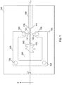
Fig. 1 illustrates an example of aninterface 100 adapted to receive a RF probe (not illustrated) for testing an electric device (not illustrated) that is arranged on a same (test)substrate 199 as theinterface 100. Thesubstrate 199 serves as a substrate for the electric device and theinterface 100. For example, thesubstrate 199 may be a Printed Circuit Board (PCB) or a glass substrate. The electric device may be understood as a Device Under Test (DUT). It is to be noted that the electric device may be mounted on thesubstrate 199 or be embedded within thesubstrate 199. The RF probe may, e.g., be a Ground-Signal-Ground (GSG) probe for RF testing the electric device. - The interface comprises a first
conductive structure 110 for receiving at least one probe tip of the RF probe, and a secondconductive structure 120 for receiving at least one further probe tip of the RF probe. The firstconductive structure 110 and the secondconductive structure 120 may be coplanar, i.e. be arranged in a same layer. Alternatively, the firstconductive structure 110 and the secondconductive structure 120 may be arranged in different layers. The firstconductive structure 110 and the secondconductive structure 120 may, e.g., be metal structures. - The second
conductive structure 120 is for receiving a reference signal from the at least one further probe tip of the RF probe (e.g. a ground reference from two further probe tips of the RF probe). In order to provide the reference signal to the electric device, the secondconductive structure 120 electrically couples to the electric device by one or more vias of the substrate. In the example ofFig. 1 , the secondconductive structure 120 electrically couples to fourvias conductive structure 110 is for receiving a test signal from the at least one probe tip of the RF probe. In other words, the at least one probe tip is used to apply a test signal to theinterface 100 and, hence, the electric device. Therefore, the firstconductive structure 110 is coupled at afirst end 111 to asignal line 150 on thesubstrate 199 that couples to the electric device. In other words, the firstconductive structure 110 is coupled to the electric device via thesignal line 150. Thesignal line 150 is a conductive path routed on the substrate (e.g. the surface of the substrate). For example, thesignal line 150 may be a MicroStrip Line (MSL). - It is to be noted that the above mentioned GSG probe is merely an example for an RF probe. In general any type of RF probe may be used. For example, an RF probe comprising only a probe tip for applying a test signal to the first
conductive structure 110, and only one other probe tip for applying a reference signal to the secondconductive structure 120 may be used. Further, it is to be noted that in alternative examples, one or more additional signal lines (e.g. coplanar to transmission line 150) may be used for coupling the secondconductive structure 120 to the electric device instead of the vias illustrated inFig. 1 . - The first
conductive structure 110 is for instance strip-shaped. The term "strip-shaped" is to be understood such that a dimension (extension) of an element such as firstconductive structure 110 along a spatial axis is much greater (e.g. at least two, three, four, five, ten, twenty, fifty or one hundred times greater) than a dimension of the element along another spatial axis which is orthogonal to the spatial axis. In the example ofFig. 1 , the firstconductive structure 110 extends lengthwise along a spatial axisx such that the dimension of the firstconductive structure 110 along the spatial axisx is much greater than the dimension of the firstconductive structure 110 along the other spatial axisy which is orthogonal to the spatial axisx . - When the RF probe is placed on the first
conductive structure 110, any conductive structure or material forming the signal path between thesignal line 150 and the position at which the RF probe is placed on (touches) the firstconductive structure 110 leads to a (small) series inductance Lfeed (seeFig. 2 ). For example, part of the firstconductive structure 110 as well as theshort interconnection 170 between the firstconductive structure 110 and thesignal line 150 may cause the series inductance Lfeed in the example ofFig. 1 . The series inductance together with the capacitance CTL of thesignal line 150 causes unwanted RF parasitics at the interface. These RF parasitics become especially problematic when the dimensions of theinterface 100 and/or the probe have an order of magnitude which is close or equal to that of the wavelength of the test signal (e.g. when they differ from two orders of magnitude or less or are of the same order of magnitude). - In order to overcome the parasitics, the
interface 100 further comprises acapacitive element 140 for providing a compensation capacitance Ccompensate. Thecapacitive element 140 and the firstconductive structure 110 are electrically coupled in order to form a compensation network for compensating the RF parasitics. Thecapacitive element 140 is not in electrical contact with the secondconductive structure 120 since thecapacitive element 140 does not touch the secondconductive structure 120. Thecapacitive element 140 electrically couples (is attached) to asecond end 112 of the firstconductive structure 110. As can be seen fromFig. 1 , thecapacitive element 140 and thesignal line 150 are arranged on opposite sides of each of the firstconductive structure 110 along the spatial axisx . In other words, a compensation capacitance Ccompensate is added at the RF probe side of the structure illustrated inFig. 1 . - An equivalent circuit of the example depicted in
Fig. 1 is illustrated inFig. 2 . The inherent capacitance of thesignal line 150 is represented by the capacitance CTL. - The
capacitive element 140 adds a compensation capacitance Ccompensate such that the series inductance Lfeed and the compensation capacitance Ccompensate of thecapacitive element 140 form an LC compensation network that allows to compensate at least in part for the unwanted RF parasitics caused by the series inductance Lfeed and the capacitance CTL of thesignal line 150. In other words, the compensation capacitance Ccompensate of thecapacitive element 140 may allow to compensate for the series inductance Lfeed. The compensation capacitance Ccom-pensate of thecapacitive element 140 may allow for a significantly increased bandwidth of theinterface 100 compared to conventional launcher structures. In other words, the proposed incorporation of an LC compensation network into the launcher structure may allow to compensate for RF probe-to-substrate transition related parasitics. - In the example of
Fig. 1 , the secondconductive structure 120 is formed integrally such thatend portions conductive structure 120 are arranged on opposite sides of the spatial axisx . The secondconductive structure 120 defines aninner space 130 within which thecapacitive element 140 is arranged. All or part of the firstconductive structure 110 may also be arranged within theinner space 130. Furthermore, the shape of the secondconductive structure 120 is symmetrical with respect to the spatial axisx . It is to be noted that the respective locations of thevias 101, ..., 104 need not be symmetrical with respect to the spatial axisx . In alternative examples, the shape of the secondconductive structure 120 may be asymmetrical with respect to the spatial axisx . - The
capacitive element 140 may be implemented in many different ways. For example, thecapacitive element 140 may be implemented with a fixed, predetermined capacitance or with an adjustable capacitance (e.g. depending on the frequency of the test signal to be applied via the first conductive structure 110). In the example ofFig. 1 which depicts a configuration in which the capacitance is fixed, thecapacitive element 140 is a metal pad (patch) of a predefined capacitance (e.g. the desired compensation capacitance Ccompensate). However, thecapacitive element 140 may alternatively be formed by any other suitable electrically conductive material such as electrically conductive ceramics. - As can be seem from
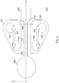
Fig. 1 , the metal pad is irregularly shaped. It is to be noted that thecapacitive element 140 may, in general, be of arbitrary shape. In other examples, the capacitive element may be of rectangular shape as indicated by thecapacitive element 340 ofinterface 300 illustrated inFig. 3 . In alternative examples, the capacitive element may be of circular shape as indicated by thecapacitive element 440 ofinterface 400 illustrated inFig. 4 . - In the example of
Figs. 3 and4 , the secondconductive structure 120 is not formed integrally, i.e. the secondconductive structure 120 does not consist of a single conductive element. The second conductive structures of theinterfaces first sub-structure 123 and asecond sub-structure 124. The first and thesecond sub-structure x and are electrically separated from each other. Again, thecapacitive element 140 is not in electrical contact with the first and thesecond sub-structure capacitive element 140 does not touch the first and thesecond sub-structure Figs. 3 and4 , shapes of the first and thesecond sub-structure x . However, in alternative examples, the shapes of the first and thesecond sub-structure x . For example, due to the presence of another structure on the substrate, one of the first and thesecond sub-structure conductive structure 120 illustrated inFig. 1 . Similarly, thevias 101 to 104 may be placed in a non-symmetric manner, as indicated above. - In alternative examples as illustrated in
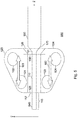
Fig. 5 , the firstconductive structure 110 presents an extendingportion 113 that extends along the spatial axisx beyond vertical projections of the first and thesecond sub-structure x . The vertical projections of the first and thesecond sub-structure x are indicated by dashedlines Fig. 5 . At least part of the extendingportion 113 forms thecapacitive element 540. In theinterface 500 ofFig. 5 , the firstconductive structure 110 is prolonged in order to provide acapacitive element 540 with the desired compensation capacitance Ccompen-sate at an opposite end of the firstconductive structure 110 compared to theinterconnection 170 to thesignal line 150. In other words, the capacitive element may be a lengthwise prolongation of the firstconductive structure 110, whose dimension along the spatial axis is chosen so that the compensation capacitance exhibits a target value. - In other examples, the capacitive element may be (comprise) a (active) MEMS capacitor as illustrated in
Fig. 6. Fig. 6 illustrates anotherinterface 600 comprising aMEMS capacitor 640 coupled to thesecond end 112 of the firstconductive structure 110. A MEMS capacitor is a capacitor manufactured in MicroElectroMechanical Systems (MEMS) technology. A distance (gap) between electrodes of theMEMS capacitor 640 is adjustable based on one or more control signals 641 (e.g. the number of control signal may depend on the implementation of the MEMS capacitor 640) for adjusting a capacitance of the MEMS capacitor 640 (e.g. to the desired compensation capacitance Ccompensate). In other words, theMEMS capacitor 640 is configured to receive one ormore control signals 641 for adjusting an adjustable capacitance of the MEMS capacitor 640 (e.g. the MEMS capacitance may be adjusted via DC biasing). - Further, as indicated in an exemplary manner by the
arrows Figs. 3 to 6 , the position of the RF probe along the longitudinal extension of the first conductive structure 110 (i.e. along the spatial axisx ) may be varied to fine-tune the compensation capacitance. The position of the RF probe, i.e. the probe tips, on the interface is indicated byline 160 inFigs. 3 to 6 . By shifting the position along the spatial axisx , the compensation capacitance Ccompen-sate effectively seen by the RF probe may be fine-tuned. In other words, the smart grounding concept indicated by thearrows - In the examples described above in connection with
Figs. 1 and3 to 6 , the firstconductive structure 110 is substantially strip-shaped. However, the firstconductive structure 110 may in general exhibit any shape. An example of a dumbbell-shaped firstconductive structure 110 is illustrated inFig. 7. Fig. 7 illustrates anotherinterface 700 comprising the dumbbell-shaped firstconductive structure 110. Further,Fig. 7 illustrates that the individual elements of an interface according to the proposed technique may be arranged in different layers on the substrate. In the example ofFig. 7 , the firstconductive structure 110 and thesub-structure capacitive element 740 and thesignal line 150 are arranged in two other layers. The firstconductive structure 110 is in electrical contact with thecapacitive element 740 and thesignal line 150 viarespective vias Fig. 7 additionally illustrates that the number of vias coupled to the second conductive structure may be arbitrarily chosen. While in each of the examples described above in connection withFigs. 1 and3 to 6 four vias are coupled to the second conductive structure, only two vias are coupled to thesub-structures sub-structures Figs. 3 to 6 . It is to be noted that the shapes of thesub-structures - An effect of the proposed LC compensation network is illustrated in
Fig. 8. Fig. 8 illustrates an exemplary comparison of the reflection losses for an interface according to the proposed technique and a conventional launcher structure. - The reflection loss for the interface according to the proposed technique is indicated by scattering parameter S11 denoting the ratio between the signal power reflected by the interface and the signal power input to the interface.
Line 810 represents the course of the scattering parameter S11 for the interface over an exemplary frequency range from 0 GHz to 110 GHz. It is to be noted that the proposed LC compensation network is not limited to the exemplary frequency range illustrated inFig. 8 . In general, the proposed LC compensation network may be used for any frequency range. - As a reference, the reflection loss for a conventional launcher structure at a frequency of 80 GHz is indicated in
Fig. 8 by means ofdouble arrow 820. A conventional launcher structure typically shows a reflection loss of about -5 to -10 dB as indicated by thedouble arrow 820. - It can be seen from
Fig. 8 that the proposed interface shows a reflection loss of about -19 dB. That is, the proposed interface is more "transparent" for measurement signals than a conventional launcher structure. Further,Fig. 8 shows that the reflection loss is well below -15 dB over the whole exemplary frequency range from 0 GHz to 110 GHz. The low reflection loss helps achieving a low insertion loss. Therefore, the proposed interface may allow broadband RF measurement/characterization of an electronic device with high performance (i.e. higher measurement accuracy). - An electric system comprising an electric device and an interface according to the proposed concept arranged on the same substrate may allow broadband RF measurement/characterization of the electronic device with high performance.
- An example of a
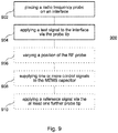
method 900 for testing an electric device arranged on a substrate according to the proposed technique is further illustrated inFig. 9 .Method 900 comprises placing 902 a RF probe onto an interface as described above. In other words,method 900 comprises placing 902 a RF probe onto an interface arranged on the substrate such that a first conductive structure of the interface receives at least one probe tip of the RF probe and that a second conductive structure of the interface receives at least one further probe tip of the RF probe. The first conductive structure is coupled to a signal line on the substrate that couples to the electric device. The first conductive structure and a capacitive element for providing a compensation capacitance are electrically coupled in order to form a compensation network for compensating RF parasitics.Method 900 additionally comprises applying 904 a test signal to the interface via the at least one probe tip. - Using the proposed interface,
method 900 may allow to overcome RF parasitics over a wide frequency range. Accordingly,method 900 may allow broadband RF measurement/characterization of the electronic device with high performance, i.e. low signal loss and signal reflections at the interface between the RF probe and the substrate. - As indicated above, the position of the RF probe along the interface may be varied in order to fine-tune the compensation capacitance.
Method 900 may, hence, comprise varying 906 a position of the RF probe along a longitudinal extension of the first conductive structure. - If the capacitive element comprises a MEMS capacitor exhibiting an adjustable capacitance,
method 900 may additionally comprise supplying 908 one or more control signals to the MEMS capacitor for adjusting the adjustable capacitance of the MEMS capacitor (e.g. to a predefined capacitance). - Further, the at least one further probe tip of the RF probe may be used for providing a reference signal such as a ground reference. Therefore,
method 900 may optionally further comprise applying 910 a reference signal to the interface via the at least one further probe tip. - More details and aspects of
method 900 are explained in connection with the proposed technique or one or more examples described above.Method 900 may comprise one or more additional optional features corresponding to one or more aspects of the proposed technique or one or more examples described above. - An exemplary set-up for a GSG measurement according to
method 900 is illustrated inFig. 10 . ARF probe 1010 is placed ontointerface 1020 as described above in connection withFig. 4 . Accordingly, a firstconductive structure 1021 of the interface receives theprobe tip 1011 of theRF probe 1010. The second conductive structure of theinterface 1020 comprises afirst sub-structure 1022 and asecond sub-structure 1023. Each of thefirst sub-structure 1022 and thesecond sub-structure 1023 receives a respective one of thefurther probe tips RF probe 1010. - A test signal is applied to the
interface 1020 via theprobe tip 1011, wherein a ground reference (as an example of a reference signal) is applied to the interface via thefurther probe tips interface 1020 in accordance withmethod 900. - The examples as described herein may be summarized as follows:
Some examples relate to an interface adapted to receive a RF probe for testing an electric device that is arranged on a same substrate as the interface. The interface comprises a first conductive structure for receiving at least one probe tip of the RF probe. The first conductive structure is coupled to a signal line in or on the substrate that couples to the electric device. Further, the interface comprises a second conductive structure for receiving at least one further probe tip of the RF probe. The interface additionally comprises a capacitive element for providing a compensation capacitance. The capacitive element and the first conductive structure are electrically coupled in order to form a compensation network for compensating RF parasitics. - In some examples, the capacitive element is not in electrical contact with the second conductive structure.
- According to some examples, the first conductive structure extends lengthwise along a spatial axis, wherein the capacitive element and the signal line are arranged on opposite sides of the first conductive structure along the spatial axis.
- In some examples, the second conductive structure defines an inner space within which the capacitive element is arranged.
- According to some examples, the second conductive structure is formed integrally such that end portions of the second conductive structure are arranged on opposite sides of the spatial axis.
- In alternative examples, the second conductive structure comprises a first sub-structure and a second sub-structure, wherein the first and the second sub-structure are arranged on opposite sides of the spatial axis and are electrically separated from each other.
- According to some examples, shapes of the first and the second sub-structure are symmetrical with respect to the spatial axis.
- In some examples, shapes of the first and the second sub-structure are asymmetrical with respect to the spatial axis.
- According to some examples, the first conductive structure presents an extending portion that extends along the spatial axis beyond vertical projections of the first and the second sub-structure onto the spatial axis, wherein at least part of the extending portion forms the capacitive element.
- In some examples, the capacitive element is a pad of electrically conductive material.
- In alternative examples, the capacitive element comprises a MEMS capacitor configured to receive one or more control signals for adjusting an adjustable capacitance of the MEMS capacitor.
- According to some examples, the first conductive structure and the second conductive structure are coplanar.
- In some examples, the second conductive structure electrically couples to one or more vias of the substrate coupled to the electric device.
- Another example relates to an electric system comprising an electric device arranged on a substrate, and an interface as described herein which is arranged on the substrate.
- A further example relates to a method for testing an electric device arranged on a substrate. The method comprises placing a RF probe onto an interface arranged on the substrate such that a first conductive structure of the interface receives at least one probe tip of the RF probe and that a second conductive structure of the interface receives at least one further probe tip of the RF probe. The first conductive structure is coupled to a signal line on the substrate that couples to the electric device. The first conductive structure and a capacitive element for providing a compensation capacitance are electrically coupled in order to form a compensation network for compensating RF parasitics. The method additionally comprises applying a test signal to the interface via the at least one probe tip.
- According to some examples, the method further comprises varying a position of the at least one probe tip along a longitudinal extension of the first conductive structure.
- In some examples, the capacitive element comprises a MEMS capacitor exhibiting an adjustable capacitance, wherein the method further comprises supplying one or more control signals to the MEMS capacitor for adjusting the adjustable capacitance of the MEMS capacitor.
- According to some examples, the method further comprises applying a reference signal to the interface via the at least one further probe tip.
- Examples according to the proposed technique may allow to overcome parasitics of an RF probe interface by usage of an LC compensation network.
- The aspects and features mentioned and described together with one or more of the previously detailed examples and figures, may as well be combined with one or more of the other examples in order to replace a like feature of the other example or in order to additionally introduce the feature to the other example.
- The description and drawings merely illustrate the principles of the disclosure. Furthermore, all examples recited herein are principally intended expressly to be only for illustrative purposes to aid the reader in understanding the principles of the disclosure and the concepts contributed by the inventor(s) to furthering the art. All statements herein reciting principles, aspects, and examples of the disclosure, as well as specific examples thereof, are intended to encompass equivalents thereof.
- A block diagram may, for instance, illustrate a high-level circuit diagram implementing the principles of the disclosure. Methods disclosed in the specification or in the claims may be implemented by a device having means for performing each of the respective acts of these methods.
- It is to be understood that the disclosure of multiple acts, processes, operations, steps or functions disclosed in the specification or claims may not be construed as to be within the specific order, unless explicitly or implicitly stated otherwise, for instance for technical reasons. Therefore, the disclosure of multiple acts or functions will not limit these to a particular order unless such acts or functions are not interchangeable for technical reasons. Furthermore, in some examples a single act, function, process, operation or step may include or may be broken into multiple sub-acts, -functions, -processes, -operations or -steps, respectively. Such sub acts may be included and part of the disclosure of this single act unless explicitly excluded.
- Furthermore, the following claims are hereby incorporated into the detailed description, where each claim may stand on its own as a separate example. While each claim may stand on its own as a separate example, it is to be noted that - although a dependent claim may refer in the claims to a specific combination with one or more other claims - other examples may also include a combination of the dependent claim with the subject matter of each other dependent or independent claim. Such combinations are explicitly proposed herein unless it is stated that a specific combination is not intended. Furthermore, it is intended to include also features of a claim to any other independent claim even if this claim is not directly made dependent to the independent claim.
Claims (15)
- An interface (100) adapted to receive a radio frequency probe for testing an electric device that is arranged on a same substrate (199) as the interface (100), the interface (100) comprising:a first conductive structure (110) for receiving at least one probe tip of the radio frequency probe, wherein the first conductive structure (110) is coupled to a signal line (150) in or on the substrate (199) that couples to the electric device;a second conductive structure (120) for receiving at least one further probe tip of the radio frequency probe; anda capacitive element (140) for providing a compensation capacitance, wherein the capacitive element (140) and the first conductive structure (110) are electrically coupled in order to form a compensation network for compensating radio frequency parasitics.
- The interface (100) of claim 1, wherein the capacitive element (140) is not in electrical contact with the second conductive structure (120).
- The interface (100) of claim 1 or claim 2, wherein the first conductive structure (110) extends lengthwise along a spatial axis (
x ), and wherein the capacitive element (140) and the signal line (150) are arranged on opposite sides of the first conductive structure (110) along the spatial axis (x ). - The interface (100) of claim 3, wherein the second conductive structure (120) defines an inner space within which the capacitive element (140) is arranged.
- The interface (100) of claim 3 or claim 4, wherein the second conductive structure (120) is formed integrally such that end portions (121, 122) of the second conductive structure (120) are arranged on opposite sides of the spatial axis (
x ). - The interface (100) of claim 3, wherein the second conductive structure (120) comprises a first sub-structure (123) and a second sub-structure (124), wherein the first and the second sub-structure (123, 124) are arranged on opposite sides of the spatial axis (
x ) and are electrically separated from each other. - The interface (100) of claim 6, wherein shapes of the first and the second sub-structure (123, 124) are symmetrical with respect to the spatial axis (
x ). - The interface (100) of claim 6 or claim 7, wherein the first conductive structure (110) presents an extending portion (113) that extends along the spatial axis (
x ) beyond vertical projections of the first and the second sub-structure (123, 124) onto the spatial axis (x ), and wherein at least part of the extending portion (113) forms the capacitive element (140). - The interface (100) of any of claim 1 to 8, wherein the capacitive element (140) is a pad of electrically conductive material.
- The interface (100) of any of claim 1 to 8, wherein the capacitive element (140) comprises a MEMS capacitor (640) configured to receive one or more control signals (641) for adjusting an adjustable capacitance of the MEMS capacitor.
- The interface (100) of any of claims 1 to 10, wherein the first conductive structure (110) and the second conductive structure (120) are coplanar.
- An electric system, comprising:an electric device arranged on a substrate (199); andan interface (100) according to any of claims 1 to 11 arranged on the substrate (199).
- A method (900) for testing an electric device arranged on a substrate, the method (900) comprising:placing (902) a radio frequency probe onto an interface arranged on the substrate such that a first conductive structure of the interface receives at least one probe tip of the radio frequency probe and that a second conductive structure of the interface receives at least one further probe tip of the radio frequency probe, wherein the first conductive structure is coupled to a signal line in or on the substrate that couples to the electric device, and wherein the first conductive structure and a capacitive element for providing a compensation capacitance are electrically coupled in order to form a compensation network for compensating radio frequency parasitics; andapplying (904) a test signal to the interface via the at least one probe tip.
- The method (900) of claim 13, further comprising:
varying (906) a position of the at least one probe tip along a longitudinal extension of the first conductive structure. - The method (900) of claim 13 or claim 14, further comprising:
applying (910) a reference signal to the interface via the at least one further probe tip.
Priority Applications (1)
| Application Number | Priority Date | Filing Date | Title |
|---|---|---|---|
| EP19198097.8A EP3796013B1 (en) | 2019-09-18 | 2019-09-18 | Interface adapted to receive a radio frequency probe for testing an electric device, and method for testing an electric device arranged on a substrate |
Applications Claiming Priority (1)
| Application Number | Priority Date | Filing Date | Title |
|---|---|---|---|
| EP19198097.8A EP3796013B1 (en) | 2019-09-18 | 2019-09-18 | Interface adapted to receive a radio frequency probe for testing an electric device, and method for testing an electric device arranged on a substrate |
Publications (2)
| Publication Number | Publication Date |
|---|---|
| EP3796013A1 true EP3796013A1 (en) | 2021-03-24 |
| EP3796013B1 EP3796013B1 (en) | 2023-08-02 |
Family
ID=67997512
Family Applications (1)
| Application Number | Title | Priority Date | Filing Date |
|---|---|---|---|
| EP19198097.8A Active EP3796013B1 (en) | 2019-09-18 | 2019-09-18 | Interface adapted to receive a radio frequency probe for testing an electric device, and method for testing an electric device arranged on a substrate |
Country Status (1)
| Country | Link |
|---|---|
| EP (1) | EP3796013B1 (en) |
Citations (9)
| Publication number | Priority date | Publication date | Assignee | Title |
|---|---|---|---|---|
| US20060145308A1 (en) * | 2005-01-05 | 2006-07-06 | International Business Machines Corporation | On-chip circuit pad structure |
| US20100041361A1 (en) * | 2008-08-14 | 2010-02-18 | Adedayo Ojo | Method and system for a single-ended input low noise amplifier with differential output |
| US20130277803A1 (en) * | 2010-12-20 | 2013-10-24 | Stmicroelectronics S.R.L. | Connection structure for an integrated circuit with capacitive function |
| EP2745301A1 (en) * | 2011-08-19 | 2014-06-25 | Cavendish Kinetics Inc. | Routing of mems variable capacitors for rf applications |
| US20150145098A1 (en) * | 2011-12-30 | 2015-05-28 | Nanyang Technological University | Miniature passive structures, high frequency electrostatic discharge protection networks, and high frequency electrostatic discharge protection schemes |
| EP3182618A1 (en) * | 2015-12-15 | 2017-06-21 | Intel IP Corporation | Apparatus for reducing a magnetic coupling between a first electronic circuit and a second electronic circuit |
| US20180006618A1 (en) * | 2016-06-29 | 2018-01-04 | Skyworks Solutions, Inc. | Active cross-band isolation for a transformer-based power amplifier |
| JP2018137296A (en) * | 2017-02-20 | 2018-08-30 | 住友電気工業株式会社 | High frequency equipment |
| US20190120876A1 (en) * | 2017-10-20 | 2019-04-25 | Formfactor, Inc. | Direct Metalized Guide Plate |
-
2019
- 2019-09-18 EP EP19198097.8A patent/EP3796013B1/en active Active
Patent Citations (9)
| Publication number | Priority date | Publication date | Assignee | Title |
|---|---|---|---|---|
| US20060145308A1 (en) * | 2005-01-05 | 2006-07-06 | International Business Machines Corporation | On-chip circuit pad structure |
| US20100041361A1 (en) * | 2008-08-14 | 2010-02-18 | Adedayo Ojo | Method and system for a single-ended input low noise amplifier with differential output |
| US20130277803A1 (en) * | 2010-12-20 | 2013-10-24 | Stmicroelectronics S.R.L. | Connection structure for an integrated circuit with capacitive function |
| EP2745301A1 (en) * | 2011-08-19 | 2014-06-25 | Cavendish Kinetics Inc. | Routing of mems variable capacitors for rf applications |
| US20150145098A1 (en) * | 2011-12-30 | 2015-05-28 | Nanyang Technological University | Miniature passive structures, high frequency electrostatic discharge protection networks, and high frequency electrostatic discharge protection schemes |
| EP3182618A1 (en) * | 2015-12-15 | 2017-06-21 | Intel IP Corporation | Apparatus for reducing a magnetic coupling between a first electronic circuit and a second electronic circuit |
| US20180006618A1 (en) * | 2016-06-29 | 2018-01-04 | Skyworks Solutions, Inc. | Active cross-band isolation for a transformer-based power amplifier |
| JP2018137296A (en) * | 2017-02-20 | 2018-08-30 | 住友電気工業株式会社 | High frequency equipment |
| US20190120876A1 (en) * | 2017-10-20 | 2019-04-25 | Formfactor, Inc. | Direct Metalized Guide Plate |
Non-Patent Citations (2)
| Title |
|---|
| CHANG D-C ET AL: "K-Band Low-Noise Amplifiers Using 0.18>tex<$murm m$>/tex<CMOS Technology", IEEE MICROWAVE AND WIRELESS COMPONENTS LETTERS, IEEE SERVICE CENTER, NEW YORK, NY, US, vol. 14, no. 3, 1 March 2004 (2004-03-01), pages 106 - 108, XP011109481, ISSN: 1531-1309, DOI: 10.1109/LMWC.2004.825175 * |
| VASSILEV V ET AL: "ESD-RF co-design methodology for the state of the art RF-CMOS blocks", MICROELECTRONICS AND RELIABILITY, ELSEVIER SCIENCE LTD, GB, vol. 45, no. 2, 1 February 2005 (2005-02-01), pages 255 - 268, XP004708564, ISSN: 0026-2714, DOI: 10.1016/J.MICROREL.2004.05.013 * |
Also Published As
| Publication number | Publication date |
|---|---|
| EP3796013B1 (en) | 2023-08-02 |
Similar Documents
| Publication | Publication Date | Title |
|---|---|---|
| KR100864916B1 (en) | Probes for Testing Devices Under Test | |
| CA2828426C (en) | Impedance tuner systems and probes | |
| US7116121B1 (en) | Probe assembly with controlled impedance spring pin or resistor tip spring pin contacts | |
| US7034544B2 (en) | Methods for minimizing the impedance discontinuity between a conductive trace and a component and structures formed thereby | |
| US20030218516A1 (en) | Miniature directional coupler | |
| US9804195B2 (en) | HF measuring probe contacting assembly | |
| CN105548771A (en) | LTCC filter testing board and testing clamping tool | |
| US9772350B2 (en) | RF probe | |
| US11460485B2 (en) | Direct metalized guide plate | |
| US7940067B2 (en) | Probe with printed tip | |
| JP7842038B2 (en) | Multiconductor transmission line probe | |
| EP2363720B1 (en) | Method of manufacture of an integrated circuit package | |
| US20130249653A1 (en) | Tunable High-Frequency Transmission Line | |
| EP3796013B1 (en) | Interface adapted to receive a radio frequency probe for testing an electric device, and method for testing an electric device arranged on a substrate | |
| CN109870596B (en) | Test and Measurement Probe Couplers | |
| JP7065502B2 (en) | Dielectric material evaluation device | |
| CN117374538A (en) | An electrically adjustable equalizer with constant insertion loss in high frequency bands | |
| JP7370060B2 (en) | Evaluation method, evaluation device, and evaluation system for dielectric materials | |
| Freidl et al. | Design of PCB RF probe landing pads for measurements up to 90 GHz | |
| US9099763B2 (en) | Tunable slow wave coplanar waveguide transmission line having a movable shielding plane | |
| Shinde et al. | Electro-mechanical structures for channel emulation | |
| Devi et al. | A novel design of 4-bit distributed MEMS transmission line (DMTL) phase shifter using an RF shunt capacitive MEMS switch for phased array antenna | |
| WO2005101034A1 (en) | Method and instrument for measuring high-frequency electric characteristic of electronic component, and method for calibrating high-frequency electrical characteristic measuring instrument | |
| JP6146043B2 (en) | Measuring apparatus and measuring method | |
| JP5675461B2 (en) | Probe, measuring device, and circuit board |
Legal Events
| Date | Code | Title | Description |
|---|---|---|---|
| PUAI | Public reference made under article 153(3) epc to a published international application that has entered the european phase |
Free format text: ORIGINAL CODE: 0009012 |
|
| STAA | Information on the status of an ep patent application or granted ep patent |
Free format text: STATUS: THE APPLICATION HAS BEEN PUBLISHED |
|
| AK | Designated contracting states |
Kind code of ref document: A1 Designated state(s): AL AT BE BG CH CY CZ DE DK EE ES FI FR GB GR HR HU IE IS IT LI LT LU LV MC MK MT NL NO PL PT RO RS SE SI SK SM TR |
|
| AX | Request for extension of the european patent |
Extension state: BA ME |
|
| STAA | Information on the status of an ep patent application or granted ep patent |
Free format text: STATUS: REQUEST FOR EXAMINATION WAS MADE |
|
| 17P | Request for examination filed |
Effective date: 20210809 |
|
| RBV | Designated contracting states (corrected) |
Designated state(s): AL AT BE BG CH CY CZ DE DK EE ES FI FR GB GR HR HU IE IS IT LI LT LU LV MC MK MT NL NO PL PT RO RS SE SI SK SM TR |
|
| GRAP | Despatch of communication of intention to grant a patent |
Free format text: ORIGINAL CODE: EPIDOSNIGR1 |
|
| STAA | Information on the status of an ep patent application or granted ep patent |
Free format text: STATUS: GRANT OF PATENT IS INTENDED |
|
| INTG | Intention to grant announced |
Effective date: 20230324 |
|
| GRAS | Grant fee paid |
Free format text: ORIGINAL CODE: EPIDOSNIGR3 |
|
| GRAA | (expected) grant |
Free format text: ORIGINAL CODE: 0009210 |
|
| STAA | Information on the status of an ep patent application or granted ep patent |
Free format text: STATUS: THE PATENT HAS BEEN GRANTED |
|
| AK | Designated contracting states |
Kind code of ref document: B1 Designated state(s): AL AT BE BG CH CY CZ DE DK EE ES FI FR GB GR HR HU IE IS IT LI LT LU LV MC MK MT NL NO PL PT RO RS SE SI SK SM TR |
|
| REG | Reference to a national code |
Ref country code: GB Ref legal event code: FG4D |
|
| REG | Reference to a national code |
Ref country code: CH Ref legal event code: EP |
|
| REG | Reference to a national code |
Ref country code: DE Ref legal event code: R096 Ref document number: 602019033918 Country of ref document: DE |
|
| REG | Reference to a national code |
Ref country code: IE Ref legal event code: FG4D |
|
| REG | Reference to a national code |
Ref country code: LT Ref legal event code: MG9D |
|
| P01 | Opt-out of the competence of the unified patent court (upc) registered |
Effective date: 20231019 |
|
| REG | Reference to a national code |
Ref country code: NL Ref legal event code: MP Effective date: 20230802 |
|
| REG | Reference to a national code |
Ref country code: AT Ref legal event code: MK05 Ref document number: 1595390 Country of ref document: AT Kind code of ref document: T Effective date: 20230802 |
|
| PG25 | Lapsed in a contracting state [announced via postgrant information from national office to epo] |
Ref country code: GR Free format text: LAPSE BECAUSE OF FAILURE TO SUBMIT A TRANSLATION OF THE DESCRIPTION OR TO PAY THE FEE WITHIN THE PRESCRIBED TIME-LIMIT Effective date: 20231103 |
|
| PG25 | Lapsed in a contracting state [announced via postgrant information from national office to epo] |
Ref country code: IS Free format text: LAPSE BECAUSE OF FAILURE TO SUBMIT A TRANSLATION OF THE DESCRIPTION OR TO PAY THE FEE WITHIN THE PRESCRIBED TIME-LIMIT Effective date: 20231202 |
|
| PG25 | Lapsed in a contracting state [announced via postgrant information from national office to epo] |
Ref country code: SE Free format text: LAPSE BECAUSE OF FAILURE TO SUBMIT A TRANSLATION OF THE DESCRIPTION OR TO PAY THE FEE WITHIN THE PRESCRIBED TIME-LIMIT Effective date: 20230802 Ref country code: RS Free format text: LAPSE BECAUSE OF FAILURE TO SUBMIT A TRANSLATION OF THE DESCRIPTION OR TO PAY THE FEE WITHIN THE PRESCRIBED TIME-LIMIT Effective date: 20230802 Ref country code: PT Free format text: LAPSE BECAUSE OF FAILURE TO SUBMIT A TRANSLATION OF THE DESCRIPTION OR TO PAY THE FEE WITHIN THE PRESCRIBED TIME-LIMIT Effective date: 20231204 Ref country code: NO Free format text: LAPSE BECAUSE OF FAILURE TO SUBMIT A TRANSLATION OF THE DESCRIPTION OR TO PAY THE FEE WITHIN THE PRESCRIBED TIME-LIMIT Effective date: 20231102 Ref country code: NL Free format text: LAPSE BECAUSE OF FAILURE TO SUBMIT A TRANSLATION OF THE DESCRIPTION OR TO PAY THE FEE WITHIN THE PRESCRIBED TIME-LIMIT Effective date: 20230802 Ref country code: LV Free format text: LAPSE BECAUSE OF FAILURE TO SUBMIT A TRANSLATION OF THE DESCRIPTION OR TO PAY THE FEE WITHIN THE PRESCRIBED TIME-LIMIT Effective date: 20230802 Ref country code: LT Free format text: LAPSE BECAUSE OF FAILURE TO SUBMIT A TRANSLATION OF THE DESCRIPTION OR TO PAY THE FEE WITHIN THE PRESCRIBED TIME-LIMIT Effective date: 20230802 Ref country code: IS Free format text: LAPSE BECAUSE OF FAILURE TO SUBMIT A TRANSLATION OF THE DESCRIPTION OR TO PAY THE FEE WITHIN THE PRESCRIBED TIME-LIMIT Effective date: 20231202 Ref country code: HR Free format text: LAPSE BECAUSE OF FAILURE TO SUBMIT A TRANSLATION OF THE DESCRIPTION OR TO PAY THE FEE WITHIN THE PRESCRIBED TIME-LIMIT Effective date: 20230802 Ref country code: GR Free format text: LAPSE BECAUSE OF FAILURE TO SUBMIT A TRANSLATION OF THE DESCRIPTION OR TO PAY THE FEE WITHIN THE PRESCRIBED TIME-LIMIT Effective date: 20231103 Ref country code: FI Free format text: LAPSE BECAUSE OF FAILURE TO SUBMIT A TRANSLATION OF THE DESCRIPTION OR TO PAY THE FEE WITHIN THE PRESCRIBED TIME-LIMIT Effective date: 20230802 Ref country code: AT Free format text: LAPSE BECAUSE OF FAILURE TO SUBMIT A TRANSLATION OF THE DESCRIPTION OR TO PAY THE FEE WITHIN THE PRESCRIBED TIME-LIMIT Effective date: 20230802 |
|
| PG25 | Lapsed in a contracting state [announced via postgrant information from national office to epo] |
Ref country code: PL Free format text: LAPSE BECAUSE OF FAILURE TO SUBMIT A TRANSLATION OF THE DESCRIPTION OR TO PAY THE FEE WITHIN THE PRESCRIBED TIME-LIMIT Effective date: 20230802 |
|
| PG25 | Lapsed in a contracting state [announced via postgrant information from national office to epo] |
Ref country code: ES Free format text: LAPSE BECAUSE OF FAILURE TO SUBMIT A TRANSLATION OF THE DESCRIPTION OR TO PAY THE FEE WITHIN THE PRESCRIBED TIME-LIMIT Effective date: 20230802 |
|
| PG25 | Lapsed in a contracting state [announced via postgrant information from national office to epo] |
Ref country code: SM Free format text: LAPSE BECAUSE OF FAILURE TO SUBMIT A TRANSLATION OF THE DESCRIPTION OR TO PAY THE FEE WITHIN THE PRESCRIBED TIME-LIMIT Effective date: 20230802 Ref country code: RO Free format text: LAPSE BECAUSE OF FAILURE TO SUBMIT A TRANSLATION OF THE DESCRIPTION OR TO PAY THE FEE WITHIN THE PRESCRIBED TIME-LIMIT Effective date: 20230802 Ref country code: ES Free format text: LAPSE BECAUSE OF FAILURE TO SUBMIT A TRANSLATION OF THE DESCRIPTION OR TO PAY THE FEE WITHIN THE PRESCRIBED TIME-LIMIT Effective date: 20230802 Ref country code: EE Free format text: LAPSE BECAUSE OF FAILURE TO SUBMIT A TRANSLATION OF THE DESCRIPTION OR TO PAY THE FEE WITHIN THE PRESCRIBED TIME-LIMIT Effective date: 20230802 Ref country code: DK Free format text: LAPSE BECAUSE OF FAILURE TO SUBMIT A TRANSLATION OF THE DESCRIPTION OR TO PAY THE FEE WITHIN THE PRESCRIBED TIME-LIMIT Effective date: 20230802 Ref country code: CZ Free format text: LAPSE BECAUSE OF FAILURE TO SUBMIT A TRANSLATION OF THE DESCRIPTION OR TO PAY THE FEE WITHIN THE PRESCRIBED TIME-LIMIT Effective date: 20230802 Ref country code: SK Free format text: LAPSE BECAUSE OF FAILURE TO SUBMIT A TRANSLATION OF THE DESCRIPTION OR TO PAY THE FEE WITHIN THE PRESCRIBED TIME-LIMIT Effective date: 20230802 |
|
| REG | Reference to a national code |
Ref country code: CH Ref legal event code: PL |
|
| REG | Reference to a national code |
Ref country code: DE Ref legal event code: R097 Ref document number: 602019033918 Country of ref document: DE |
|
| PG25 | Lapsed in a contracting state [announced via postgrant information from national office to epo] |
Ref country code: LU Free format text: LAPSE BECAUSE OF NON-PAYMENT OF DUE FEES Effective date: 20230918 |
|
| REG | Reference to a national code |
Ref country code: BE Ref legal event code: MM Effective date: 20230930 |
|
| PG25 | Lapsed in a contracting state [announced via postgrant information from national office to epo] |
Ref country code: LU Free format text: LAPSE BECAUSE OF NON-PAYMENT OF DUE FEES Effective date: 20230918 Ref country code: IT Free format text: LAPSE BECAUSE OF FAILURE TO SUBMIT A TRANSLATION OF THE DESCRIPTION OR TO PAY THE FEE WITHIN THE PRESCRIBED TIME-LIMIT Effective date: 20230802 Ref country code: MC Free format text: LAPSE BECAUSE OF FAILURE TO SUBMIT A TRANSLATION OF THE DESCRIPTION OR TO PAY THE FEE WITHIN THE PRESCRIBED TIME-LIMIT Effective date: 20230802 |
|
| PLBE | No opposition filed within time limit |
Free format text: ORIGINAL CODE: 0009261 |
|
| STAA | Information on the status of an ep patent application or granted ep patent |
Free format text: STATUS: NO OPPOSITION FILED WITHIN TIME LIMIT |
|
| REG | Reference to a national code |
Ref country code: IE Ref legal event code: MM4A |
|
| PG25 | Lapsed in a contracting state [announced via postgrant information from national office to epo] |
Ref country code: IE Free format text: LAPSE BECAUSE OF NON-PAYMENT OF DUE FEES Effective date: 20230918 |
|
| 26N | No opposition filed |
Effective date: 20240503 |
|
| PG25 | Lapsed in a contracting state [announced via postgrant information from national office to epo] |
Ref country code: CH Free format text: LAPSE BECAUSE OF NON-PAYMENT OF DUE FEES Effective date: 20230930 |
|
| PG25 | Lapsed in a contracting state [announced via postgrant information from national office to epo] |
Ref country code: IE Free format text: LAPSE BECAUSE OF NON-PAYMENT OF DUE FEES Effective date: 20230918 Ref country code: CH Free format text: LAPSE BECAUSE OF NON-PAYMENT OF DUE FEES Effective date: 20230930 Ref country code: SI Free format text: LAPSE BECAUSE OF FAILURE TO SUBMIT A TRANSLATION OF THE DESCRIPTION OR TO PAY THE FEE WITHIN THE PRESCRIBED TIME-LIMIT Effective date: 20230802 |
|
| PG25 | Lapsed in a contracting state [announced via postgrant information from national office to epo] |
Ref country code: BE Free format text: LAPSE BECAUSE OF NON-PAYMENT OF DUE FEES Effective date: 20230930 |
|
| PG25 | Lapsed in a contracting state [announced via postgrant information from national office to epo] |
Ref country code: BG Free format text: LAPSE BECAUSE OF FAILURE TO SUBMIT A TRANSLATION OF THE DESCRIPTION OR TO PAY THE FEE WITHIN THE PRESCRIBED TIME-LIMIT Effective date: 20230802 |
|
| PG25 | Lapsed in a contracting state [announced via postgrant information from national office to epo] |
Ref country code: BG Free format text: LAPSE BECAUSE OF FAILURE TO SUBMIT A TRANSLATION OF THE DESCRIPTION OR TO PAY THE FEE WITHIN THE PRESCRIBED TIME-LIMIT Effective date: 20230802 |
|
| PG25 | Lapsed in a contracting state [announced via postgrant information from national office to epo] |
Ref country code: CY Free format text: LAPSE BECAUSE OF FAILURE TO SUBMIT A TRANSLATION OF THE DESCRIPTION OR TO PAY THE FEE WITHIN THE PRESCRIBED TIME-LIMIT; INVALID AB INITIO Effective date: 20190918 |
|
| PG25 | Lapsed in a contracting state [announced via postgrant information from national office to epo] |
Ref country code: HU Free format text: LAPSE BECAUSE OF FAILURE TO SUBMIT A TRANSLATION OF THE DESCRIPTION OR TO PAY THE FEE WITHIN THE PRESCRIBED TIME-LIMIT; INVALID AB INITIO Effective date: 20190918 |
|
| PGFP | Annual fee paid to national office [announced via postgrant information from national office to epo] |
Ref country code: GB Payment date: 20250919 Year of fee payment: 7 |
|
| PGFP | Annual fee paid to national office [announced via postgrant information from national office to epo] |
Ref country code: FR Payment date: 20250922 Year of fee payment: 7 |
|
| PG25 | Lapsed in a contracting state [announced via postgrant information from national office to epo] |
Ref country code: TR Free format text: LAPSE BECAUSE OF FAILURE TO SUBMIT A TRANSLATION OF THE DESCRIPTION OR TO PAY THE FEE WITHIN THE PRESCRIBED TIME-LIMIT Effective date: 20230802 |
|
| PGFP | Annual fee paid to national office [announced via postgrant information from national office to epo] |
Ref country code: DE Payment date: 20251121 Year of fee payment: 7 |