EP3792982A1 - Dispositif electronique de puissance a super-jonction - Google Patents
Dispositif electronique de puissance a super-jonction Download PDFInfo
- Publication number
- EP3792982A1 EP3792982A1 EP20195403.9A EP20195403A EP3792982A1 EP 3792982 A1 EP3792982 A1 EP 3792982A1 EP 20195403 A EP20195403 A EP 20195403A EP 3792982 A1 EP3792982 A1 EP 3792982A1
- Authority
- EP
- European Patent Office
- Prior art keywords
- layer
- electrically conductive
- layers
- conductive layer
- junction
- Prior art date
- Legal status (The legal status is an assumption and is not a legal conclusion. Google has not performed a legal analysis and makes no representation as to the accuracy of the status listed.)
- Granted
Links
- 239000004065 semiconductor Substances 0.000 claims description 74
- 238000004519 manufacturing process Methods 0.000 claims description 29
- 239000000463 material Substances 0.000 claims description 15
- 230000005533 two-dimensional electron gas Effects 0.000 claims description 14
- 230000015572 biosynthetic process Effects 0.000 claims description 7
- 238000000034 method Methods 0.000 claims description 7
- 238000000151 deposition Methods 0.000 claims description 6
- 230000008878 coupling Effects 0.000 claims description 2
- 238000010168 coupling process Methods 0.000 claims description 2
- 238000005859 coupling reaction Methods 0.000 claims description 2
- 239000010410 layer Substances 0.000 description 202
- 239000000758 substrate Substances 0.000 description 21
- BOTDANWDWHJENH-UHFFFAOYSA-N Tetraethyl orthosilicate Chemical compound CCO[Si](OCC)(OCC)OCC BOTDANWDWHJENH-UHFFFAOYSA-N 0.000 description 11
- 230000006978 adaptation Effects 0.000 description 10
- 150000004767 nitrides Chemical class 0.000 description 10
- 229910002601 GaN Inorganic materials 0.000 description 9
- JMASRVWKEDWRBT-UHFFFAOYSA-N Gallium nitride Chemical compound [Ga]#N JMASRVWKEDWRBT-UHFFFAOYSA-N 0.000 description 9
- 238000005530 etching Methods 0.000 description 9
- 229910052581 Si3N4 Inorganic materials 0.000 description 7
- XUIMIQQOPSSXEZ-UHFFFAOYSA-N Silicon Chemical compound [Si] XUIMIQQOPSSXEZ-UHFFFAOYSA-N 0.000 description 7
- 230000015556 catabolic process Effects 0.000 description 7
- 229910052710 silicon Inorganic materials 0.000 description 7
- 239000010703 silicon Substances 0.000 description 7
- HQVNEWCFYHHQES-UHFFFAOYSA-N silicon nitride Chemical compound N12[Si]34N5[Si]62N3[Si]51N64 HQVNEWCFYHHQES-UHFFFAOYSA-N 0.000 description 7
- 108091006146 Channels Proteins 0.000 description 5
- 241001101998 Galium Species 0.000 description 5
- 239000003989 dielectric material Substances 0.000 description 5
- 230000010287 polarization Effects 0.000 description 4
- RNQKDQAVIXDKAG-UHFFFAOYSA-N aluminum gallium Chemical compound [Al].[Ga] RNQKDQAVIXDKAG-UHFFFAOYSA-N 0.000 description 3
- 230000005684 electric field Effects 0.000 description 3
- 230000000903 blocking effect Effects 0.000 description 2
- 239000002800 charge carrier Substances 0.000 description 2
- PMHQVHHXPFUNSP-UHFFFAOYSA-M copper(1+);methylsulfanylmethane;bromide Chemical compound Br[Cu].CSC PMHQVHHXPFUNSP-UHFFFAOYSA-M 0.000 description 2
- 230000008021 deposition Effects 0.000 description 2
- 238000000407 epitaxy Methods 0.000 description 2
- 229910052751 metal Inorganic materials 0.000 description 2
- 239000002184 metal Substances 0.000 description 2
- 229910018072 Al 2 O 3 Inorganic materials 0.000 description 1
- PIGFYZPCRLYGLF-UHFFFAOYSA-N Aluminum nitride Chemical compound [Al]#N PIGFYZPCRLYGLF-UHFFFAOYSA-N 0.000 description 1
- GYHNNYVSQQEPJS-UHFFFAOYSA-N Gallium Chemical compound [Ga] GYHNNYVSQQEPJS-UHFFFAOYSA-N 0.000 description 1
- 102000004129 N-Type Calcium Channels Human genes 0.000 description 1
- 108090000699 N-Type Calcium Channels Proteins 0.000 description 1
- -1 Si 3 N 4 Inorganic materials 0.000 description 1
- 229910004298 SiO 2 Inorganic materials 0.000 description 1
- 229910052782 aluminium Inorganic materials 0.000 description 1
- XAGFODPZIPBFFR-UHFFFAOYSA-N aluminium Chemical compound [Al] XAGFODPZIPBFFR-UHFFFAOYSA-N 0.000 description 1
- 239000004020 conductor Substances 0.000 description 1
- 230000007423 decrease Effects 0.000 description 1
- 238000010586 diagram Methods 0.000 description 1
- 239000002019 doping agent Substances 0.000 description 1
- 229910052733 gallium Inorganic materials 0.000 description 1
- 238000002513 implantation Methods 0.000 description 1
- 230000006911 nucleation Effects 0.000 description 1
- 238000010899 nucleation Methods 0.000 description 1
- 229910052594 sapphire Inorganic materials 0.000 description 1
- 239000010980 sapphire Substances 0.000 description 1
- HBMJWWWQQXIZIP-UHFFFAOYSA-N silicon carbide Chemical compound [Si+]#[C-] HBMJWWWQQXIZIP-UHFFFAOYSA-N 0.000 description 1
- 229910010271 silicon carbide Inorganic materials 0.000 description 1
- 239000002356 single layer Substances 0.000 description 1
- 230000002269 spontaneous effect Effects 0.000 description 1
- 230000001052 transient effect Effects 0.000 description 1
Images


Classifications
-
- H—ELECTRICITY
- H01—ELECTRIC ELEMENTS
- H01L—SEMICONDUCTOR DEVICES NOT COVERED BY CLASS H10
- H01L29/00—Semiconductor devices specially adapted for rectifying, amplifying, oscillating or switching and having potential barriers; Capacitors or resistors having potential barriers, e.g. a PN-junction depletion layer or carrier concentration layer; Details of semiconductor bodies or of electrodes thereof ; Multistep manufacturing processes therefor
- H01L29/66—Types of semiconductor device ; Multistep manufacturing processes therefor
- H01L29/86—Types of semiconductor device ; Multistep manufacturing processes therefor controllable only by variation of the electric current supplied, or only the electric potential applied, to one or more of the electrodes carrying the current to be rectified, amplified, oscillated or switched
- H01L29/861—Diodes
-
- H—ELECTRICITY
- H01—ELECTRIC ELEMENTS
- H01L—SEMICONDUCTOR DEVICES NOT COVERED BY CLASS H10
- H01L29/00—Semiconductor devices specially adapted for rectifying, amplifying, oscillating or switching and having potential barriers; Capacitors or resistors having potential barriers, e.g. a PN-junction depletion layer or carrier concentration layer; Details of semiconductor bodies or of electrodes thereof ; Multistep manufacturing processes therefor
- H01L29/02—Semiconductor bodies ; Multistep manufacturing processes therefor
- H01L29/06—Semiconductor bodies ; Multistep manufacturing processes therefor characterised by their shape; characterised by the shapes, relative sizes, or dispositions of the semiconductor regions ; characterised by the concentration or distribution of impurities within semiconductor regions
- H01L29/0603—Semiconductor bodies ; Multistep manufacturing processes therefor characterised by their shape; characterised by the shapes, relative sizes, or dispositions of the semiconductor regions ; characterised by the concentration or distribution of impurities within semiconductor regions characterised by particular constructional design considerations, e.g. for preventing surface leakage, for controlling electric field concentration or for internal isolations regions
- H01L29/0607—Semiconductor bodies ; Multistep manufacturing processes therefor characterised by their shape; characterised by the shapes, relative sizes, or dispositions of the semiconductor regions ; characterised by the concentration or distribution of impurities within semiconductor regions characterised by particular constructional design considerations, e.g. for preventing surface leakage, for controlling electric field concentration or for internal isolations regions for preventing surface leakage or controlling electric field concentration
- H01L29/0611—Semiconductor bodies ; Multistep manufacturing processes therefor characterised by their shape; characterised by the shapes, relative sizes, or dispositions of the semiconductor regions ; characterised by the concentration or distribution of impurities within semiconductor regions characterised by particular constructional design considerations, e.g. for preventing surface leakage, for controlling electric field concentration or for internal isolations regions for preventing surface leakage or controlling electric field concentration for increasing or controlling the breakdown voltage of reverse biased devices
- H01L29/0615—Semiconductor bodies ; Multistep manufacturing processes therefor characterised by their shape; characterised by the shapes, relative sizes, or dispositions of the semiconductor regions ; characterised by the concentration or distribution of impurities within semiconductor regions characterised by particular constructional design considerations, e.g. for preventing surface leakage, for controlling electric field concentration or for internal isolations regions for preventing surface leakage or controlling electric field concentration for increasing or controlling the breakdown voltage of reverse biased devices by the doping profile or the shape or the arrangement of the PN junction, or with supplementary regions, e.g. junction termination extension [JTE]
- H01L29/063—Reduced surface field [RESURF] pn-junction structures
- H01L29/0634—Multiple reduced surface field (multi-RESURF) structures, e.g. double RESURF, charge compensation, cool, superjunction (SJ), 3D-RESURF, composite buffer (CB) structures
-
- H—ELECTRICITY
- H01—ELECTRIC ELEMENTS
- H01L—SEMICONDUCTOR DEVICES NOT COVERED BY CLASS H10
- H01L27/00—Devices consisting of a plurality of semiconductor or other solid-state components formed in or on a common substrate
- H01L27/02—Devices consisting of a plurality of semiconductor or other solid-state components formed in or on a common substrate including semiconductor components specially adapted for rectifying, oscillating, amplifying or switching and having potential barriers; including integrated passive circuit elements having potential barriers
- H01L27/04—Devices consisting of a plurality of semiconductor or other solid-state components formed in or on a common substrate including semiconductor components specially adapted for rectifying, oscillating, amplifying or switching and having potential barriers; including integrated passive circuit elements having potential barriers the substrate being a semiconductor body
- H01L27/06—Devices consisting of a plurality of semiconductor or other solid-state components formed in or on a common substrate including semiconductor components specially adapted for rectifying, oscillating, amplifying or switching and having potential barriers; including integrated passive circuit elements having potential barriers the substrate being a semiconductor body including a plurality of individual components in a non-repetitive configuration
- H01L27/07—Devices consisting of a plurality of semiconductor or other solid-state components formed in or on a common substrate including semiconductor components specially adapted for rectifying, oscillating, amplifying or switching and having potential barriers; including integrated passive circuit elements having potential barriers the substrate being a semiconductor body including a plurality of individual components in a non-repetitive configuration the components having an active region in common
- H01L27/0705—Devices consisting of a plurality of semiconductor or other solid-state components formed in or on a common substrate including semiconductor components specially adapted for rectifying, oscillating, amplifying or switching and having potential barriers; including integrated passive circuit elements having potential barriers the substrate being a semiconductor body including a plurality of individual components in a non-repetitive configuration the components having an active region in common comprising components of the field effect type
- H01L27/0727—Devices consisting of a plurality of semiconductor or other solid-state components formed in or on a common substrate including semiconductor components specially adapted for rectifying, oscillating, amplifying or switching and having potential barriers; including integrated passive circuit elements having potential barriers the substrate being a semiconductor body including a plurality of individual components in a non-repetitive configuration the components having an active region in common comprising components of the field effect type in combination with diodes, or capacitors or resistors
-
- H—ELECTRICITY
- H01—ELECTRIC ELEMENTS
- H01L—SEMICONDUCTOR DEVICES NOT COVERED BY CLASS H10
- H01L29/00—Semiconductor devices specially adapted for rectifying, amplifying, oscillating or switching and having potential barriers; Capacitors or resistors having potential barriers, e.g. a PN-junction depletion layer or carrier concentration layer; Details of semiconductor bodies or of electrodes thereof ; Multistep manufacturing processes therefor
- H01L29/02—Semiconductor bodies ; Multistep manufacturing processes therefor
- H01L29/12—Semiconductor bodies ; Multistep manufacturing processes therefor characterised by the materials of which they are formed
- H01L29/20—Semiconductor bodies ; Multistep manufacturing processes therefor characterised by the materials of which they are formed including, apart from doping materials or other impurities, only AIIIBV compounds
- H01L29/201—Semiconductor bodies ; Multistep manufacturing processes therefor characterised by the materials of which they are formed including, apart from doping materials or other impurities, only AIIIBV compounds including two or more compounds, e.g. alloys
- H01L29/205—Semiconductor bodies ; Multistep manufacturing processes therefor characterised by the materials of which they are formed including, apart from doping materials or other impurities, only AIIIBV compounds including two or more compounds, e.g. alloys in different semiconductor regions, e.g. heterojunctions
-
- H—ELECTRICITY
- H01—ELECTRIC ELEMENTS
- H01L—SEMICONDUCTOR DEVICES NOT COVERED BY CLASS H10
- H01L29/00—Semiconductor devices specially adapted for rectifying, amplifying, oscillating or switching and having potential barriers; Capacitors or resistors having potential barriers, e.g. a PN-junction depletion layer or carrier concentration layer; Details of semiconductor bodies or of electrodes thereof ; Multistep manufacturing processes therefor
- H01L29/40—Electrodes ; Multistep manufacturing processes therefor
- H01L29/402—Field plates
- H01L29/404—Multiple field plate structures
-
- H—ELECTRICITY
- H01—ELECTRIC ELEMENTS
- H01L—SEMICONDUCTOR DEVICES NOT COVERED BY CLASS H10
- H01L29/00—Semiconductor devices specially adapted for rectifying, amplifying, oscillating or switching and having potential barriers; Capacitors or resistors having potential barriers, e.g. a PN-junction depletion layer or carrier concentration layer; Details of semiconductor bodies or of electrodes thereof ; Multistep manufacturing processes therefor
- H01L29/66—Types of semiconductor device ; Multistep manufacturing processes therefor
- H01L29/66007—Multistep manufacturing processes
- H01L29/66075—Multistep manufacturing processes of devices having semiconductor bodies comprising group 14 or group 13/15 materials
- H01L29/66083—Multistep manufacturing processes of devices having semiconductor bodies comprising group 14 or group 13/15 materials the devices being controllable only by variation of the electric current supplied or the electric potential applied, to one or more of the electrodes carrying the current to be rectified, amplified, oscillated or switched, e.g. two-terminal devices
- H01L29/66196—Multistep manufacturing processes of devices having semiconductor bodies comprising group 14 or group 13/15 materials the devices being controllable only by variation of the electric current supplied or the electric potential applied, to one or more of the electrodes carrying the current to be rectified, amplified, oscillated or switched, e.g. two-terminal devices with an active layer made of a group 13/15 material
- H01L29/66204—Diodes
- H01L29/66212—Schottky diodes
-
- H—ELECTRICITY
- H01—ELECTRIC ELEMENTS
- H01L—SEMICONDUCTOR DEVICES NOT COVERED BY CLASS H10
- H01L29/00—Semiconductor devices specially adapted for rectifying, amplifying, oscillating or switching and having potential barriers; Capacitors or resistors having potential barriers, e.g. a PN-junction depletion layer or carrier concentration layer; Details of semiconductor bodies or of electrodes thereof ; Multistep manufacturing processes therefor
- H01L29/66—Types of semiconductor device ; Multistep manufacturing processes therefor
- H01L29/68—Types of semiconductor device ; Multistep manufacturing processes therefor controllable by only the electric current supplied, or only the electric potential applied, to an electrode which does not carry the current to be rectified, amplified or switched
- H01L29/76—Unipolar devices, e.g. field effect transistors
- H01L29/772—Field effect transistors
- H01L29/78—Field effect transistors with field effect produced by an insulated gate
- H01L29/7801—DMOS transistors, i.e. MISFETs with a channel accommodating body or base region adjoining a drain drift region
- H01L29/7802—Vertical DMOS transistors, i.e. VDMOS transistors
- H01L29/7803—Vertical DMOS transistors, i.e. VDMOS transistors structurally associated with at least one other device
- H01L29/7806—Vertical DMOS transistors, i.e. VDMOS transistors structurally associated with at least one other device the other device being a Schottky barrier diode
-
- H—ELECTRICITY
- H01—ELECTRIC ELEMENTS
- H01L—SEMICONDUCTOR DEVICES NOT COVERED BY CLASS H10
- H01L29/00—Semiconductor devices specially adapted for rectifying, amplifying, oscillating or switching and having potential barriers; Capacitors or resistors having potential barriers, e.g. a PN-junction depletion layer or carrier concentration layer; Details of semiconductor bodies or of electrodes thereof ; Multistep manufacturing processes therefor
- H01L29/66—Types of semiconductor device ; Multistep manufacturing processes therefor
- H01L29/86—Types of semiconductor device ; Multistep manufacturing processes therefor controllable only by variation of the electric current supplied, or only the electric potential applied, to one or more of the electrodes carrying the current to be rectified, amplified, oscillated or switched
- H01L29/861—Diodes
- H01L29/872—Schottky diodes
-
- H—ELECTRICITY
- H01—ELECTRIC ELEMENTS
- H01L—SEMICONDUCTOR DEVICES NOT COVERED BY CLASS H10
- H01L29/00—Semiconductor devices specially adapted for rectifying, amplifying, oscillating or switching and having potential barriers; Capacitors or resistors having potential barriers, e.g. a PN-junction depletion layer or carrier concentration layer; Details of semiconductor bodies or of electrodes thereof ; Multistep manufacturing processes therefor
- H01L29/02—Semiconductor bodies ; Multistep manufacturing processes therefor
- H01L29/12—Semiconductor bodies ; Multistep manufacturing processes therefor characterised by the materials of which they are formed
- H01L29/20—Semiconductor bodies ; Multistep manufacturing processes therefor characterised by the materials of which they are formed including, apart from doping materials or other impurities, only AIIIBV compounds
- H01L29/2003—Nitride compounds
Definitions
- the technical field of the invention is that of power electronics.
- the present invention relates to integrated electronic circuits and in particular to integrated electronic components capable of withstanding electrical overloads.
- the diode is a classic component of power electronics because it allows the implementation of basic functions such as switching, rectification, voltage division, etc.
- the diodes have a high switching speed, a low resistivity in the on state, that is to say a high current intensity in the on state. , as well as a high breakdown voltage.
- the resistivity of a diode in the on state depends on the material of the diode which also defines the breakdown voltage of the diode.
- the voltage level converted by the switching function is limited by the breakdown voltage of the diode.
- MPS diodes ("Merged PiN Schottky” according to the acronym), or overload diode, comprising a first type of diode, for example a PIN diode ("Positive Intrinsic Negative", according to the English acronym), and a second type of diode, for example a Schottky diode, coupled in parallel.
- This architecture allows both rapid switching between the off and on states, and withstands current overloads appearing in particular in transient conditions.
- these diodes have a high cost because they are generally made from a gallium nitride (GaN) substrate.
- GaN gallium nitride
- a heterojunction is formed by the junction of two layers of semiconductor materials with different forbidden bands.
- a two-dimensional gas of electrons forms at the interface between the two layers of semiconductor material due to spontaneous polarization and piezoelectric polarization. This two-dimensional gas serves as a conduction channel within heterojunction electronic components, and allows a high current density due to its high density of charge carriers.
- the MPS 200 diode of the prior art comprises a semiconductor substrate 100, or carrier substrate, on which is produced a buffer layer 101.
- a buffer layer conventionally makes it possible to limit the lateral and vertical leakage currents in the component and better confine the two-dimensional gas of electrons at the interface of the heterojunction.
- the MPS diode 200 further comprises an intrinsic semiconductor layer 102, that is to say an unintentionally doped semiconductor layer, on which the heterojunction is produced.
- the heterojunction comprises a layer of gallium nitride (GaN) 103, a layer of aluminum-galium nitride (AlGaN) 104 and a two-dimensional electron gas 106 formed at the interface between the GaN layer 103 and the layer of AlGaN 104.
- the Schottky diode comprises a first electrode 105 in Schottky contact with the electron gas 106, forming the anode of the Schottky diode, and a second electrode 105 'in ohmic contact with the electron gas 106 and forming the cathode of the Schottky diode.
- the PIN diode comprises a first P-type implanted region 107 made in the galium nitride layer 103 and forming the anode of the PIN diode, the intrinsic layer 102 and a second N-type implanted region 108 made in the nitride layer. of galium 103, in the intrinsic layer 102 and forming the cathode of the PIN diode.
- a solution to improve the current in the on state of the MPS type diode 200 consists in slightly doping the intrinsic semiconductor layer 102 of the PIN diode.
- increasing the doping of the intrinsic zone decreases the value of the breakdown voltage of the diode.
- the value of the breakdown voltage is divided by ten.
- the invention offers a solution to the problems mentioned above by proposing an integrated electronic device allowing the passage of a high electric current in the on state and able to withstand a high voltage at its terminals in the off state.
- the bypass component comprises a superjunction.
- the combination of a Schottky diode and a super-junction component advantageously allows, in the absence of overload, a high switching speed, and in the presence of an overload, a low on-state resistivity allowing the passage of a strong current.
- the device retains very good voltage withstand since the presence of the shunt component makes it possible to avoid having to lower the voltage withstand of the diode in order to increase the current in the on state.
- the shunt component may be a side superjunction transistor having an isolated vertical gate, a drain and a source, the isolated vertical gate and the source being electrically coupled to each other so as to be at the same electrical potential.
- the source is electrically connected to the anode of the Schottky diode and the drain is electrically connected to the cathode of the Schottky diode.
- the device comprises an electrically conductive layer, the insulated vertical gate comprising a first vertical portion of the electrically conductive layer, said first portion being electrically insulated from the superjunction by a dielectric layer, the source of the transistor comprising a second portion of said electrically conductive layer.
- the production of the source and the grid in the same electrically conductive layer is advantageous because it makes the device simpler to manufacture.
- the anode of the Schottky diode may include the second portion of the electrically conductive layer.
- the anode of the diode and the gate of the transistor are made in the same electrically conductive layer and on the other hand the anode of the Schottky diode and the source of the transistor are merged, which makes the device easier to manufacture.
- the device may include a heterojunction disposed on the superjunction and having a first junction layer and a second junction layer, the two-dimensional gas of electrons being formed at the interface between the first junction layer and the second junction layer.
- the two-dimensional electron gas advantageously allows great mobility of the charge carriers and therefore contributes to increasing the switching speed of the diode.
- the second portion of the electrically conductive layer can form a Schottky contact with the two-dimensional gas of electrons, away from the ends of the first junction layer.
- the device comprises at least one field plate comprising a horizontal portion of the electrically conductive layer.
- the production of the field plates by a portion of the electrically conductive layer is advantageous because it makes the device simpler to manufacture.
- the drain of the transistor comprises a heavily doped semiconductor region of a first conductivity type, the superjunction comprising a vertical stack of alternating semiconductor layers of the first conductivity type and of semiconductor layers of a second conductivity type opposite to the first conductivity type, the first and second layers extending horizontally from the heavily doped semiconductor region to the insulated vertical gate.
- the superjunction comprises an alternation of five first layers doped with type N at a concentration of 4x10 18 cm -3 and five second layers doped with type P at a concentration of 4x10 18 cm -3 , the first and second layers each having a thickness equal to 150 nm.
- the superjunction is placed on a voltage resistance layer with a thickness equal to 3 ⁇ m and P-type doped at a concentration of 1x10 16 cm -3 .
- the cathode of the Schottky diode may have an electrically conductive layer in ohmic contact with the heavily doped semiconductor region and the two-dimensional electron gas.
- the formation of the branch component comprises the formation of a superjunction.
- the shunt component may be a side superjunction transistor having an isolated vertical gate, a drain and a source, the isolated vertical gate and the source being electrically coupled to each other so as to be at the same electrical potential.
- the source is electrically connected to the anode of the Schottky diode and the drain is electrically connected to the cathode of the Schottky diode.
- the method may include depositing an electrically conductive layer so that the insulated vertical grid has a first portion of the electrically conductive layer and the first Schottky contact includes a second portion of the electrically conductive layer.
- the method may include the production of at least one field plate comprising a third horizontal portion of the electrically conductive layer.
- FIG. 2 is a schematic representation from an electrical point of view of an integrated electronic device 1 according to one embodiment of the invention.
- the electronic device 1 is here a switch and can find applications in any kind of power electronic system, for example in a voltage step-down or in a voltage step-up.
- the integrated electronic device 1 has a first terminal B1, a second terminal B2, a Schottky-type diode 2 and a shunt component 3, the diode 2 and the shunt component 3 being coupled in parallel between the first terminal B1 and the second terminal B2.
- the shunt component is a transistor mounted as a diode, ie a transistor whose gate and source are mutually electrically coupled so as to be at the same electrical potential.
- the source of transistor 3 can be electrically connected to the anode of Schottky diode 2 and the drain of transistor 3 can be electrically connected to the cathode of Schottky diode 2.
- Diode 2 has a first threshold voltage, for example here 0.3 volts, and transistor 3 here has a second threshold voltage greater than the first threshold voltage, for example here 1.5 volts.
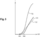
- the figure 3 represents the evolution of the intensities of the currents within the device 1 as a function of the value of the voltage V21 between the first terminal B1 and the second terminal B2 of the device 1.
- the intensity of the current I2 through the diode 2 is represented by the curve referenced C2
- the intensity of the current I3 through the transistor 3 is represented by the curve referenced C3
- the intensity of the overall current Ig flowing between the first terminal B1 and the second terminal B2 is represented by the curve referenced Cg.
- the diode 2 When the value of the voltage V21 is greater than the first threshold voltage Vs1 but less than the second threshold voltage Vs2, the diode 2 is on, the transistor 3 is blocked and therefore the device 1 is on and crossed by a current which crosses diode 2. Thus, the overall current Ig passing through the device is equal to the current I2 passing through the diode.
- the diode 2 When the value of the voltage V21 is greater than the second threshold voltage Vs2, the diode 2 is on, the transistor 3 is on and the overall current Ig flows in the device 1 through the diode 2 and the transistor 3.
- the overall current Ig flowing through the device is equal to the sum of current I2 and current I3.
- the overall current Ig flowing through device 1 is not limited by diode 2.
- FIG. 4 is a schematic sectional view of the device 1 according to one embodiment of the invention.
- the device 1 comprises a semiconductor substrate 10 supporting an active zone 11, preferably an active zone based on gallium nitride.
- the active zone 11 comprises an upper face Fs, itself surmounted by a region interconnection 12, only a part of which is detailed here for the sake of simplification.
- the substrate 10 is here an intrinsic silicon substrate. However, it would have been possible for the substrate to be a doped silicon substrate or an insulating substrate. The substrate could in particular have been made of silicon carbide or of sapphire. In the case of an active zone 11 epitaxied on silicon, the thickness of the substrate 10 is for example 1 mm for a diameter of 200 mm. The substrate 10 can however have any thickness between 400 ⁇ m and 2 mm (depending on its diameter).
- the active zone 11 is based on gallium nitride, the active zone 11 is advantageously separated from the substrate 10 by an adaptation layer 13 formed by epitaxy.
- the adaptation layer 13 acts as an intermediate between the substrate 10 and the active zone 11 and allows a mesh adaptation between the silicon of the substrate 10 and the gallium nitride of the active zone 11. It also makes it possible to absorb the stresses. mechanical between the substrate 10 and the active zone 11.
- the adaptation layer 13 conventionally comprises a layer of aluminum nitride.
- adaptation layer 13 is produced here in the form of a single layer, it could quite well comprise a plurality of stacked adaptation sublayers, and / or be produced on a nucleation sublayer, for example a layer of aluminum nitride (AlN) in contact with the substrate.
- the adaptation sublayers could include aluminum gallium nitride, the aluminum content being able to vary from one adaptation sublayer to another.
- the adaptation layer 13 is for example composed of a stack of AlN and AlGaN with a thickness of 300 nm.
- the interconnection region 12 conventionally comprises a plurality of vias and metal tracks (not shown for the purposes of simplification), as well as a superposition of first dielectric layers 121 1 , 121 2 , for example made of silicon nitride, and of second dielectric layers 120 1 , 120 2 , 120 3 , 120 4 , for example made of tetraethyl orthosilicate (TEOS).
- first dielectric layers 121 1 , 121 2 for example made of silicon nitride
- second dielectric layers 120 1 , 120 2 , 120 3 , 120 4 for example made of tetraethyl orthosilicate (TEOS).
- TEOS tetraethyl orthosilicate
- the role of the field plates is to redistribute the electric field in the device due to the equipotential lines that they generate and thus to avoid electric field peaks, thus allowing an increase in the breakdown voltage of the device 1.
- the active zone 11 comprises a voltage withstand layer 14 disposed on the matching layer 13, a superjunction 5 disposed on the voltage withstand layer 14 and a heterojunction 7 disposed on the superjunction 5.
- the superjunction 5, produced here directly on the voltage withstand layer 14, comprises a vertical stack formed of a plurality of semiconductor layers, preferably of galium nitride.
- the stack comprises an alternation of first layers 50 doped with a first type of conductivity, here an N-type conductivity, and second layers 51 doped with a second type of conductivity, here a P-type conductivity.
- the stack comprises three first N-type semiconductor layers 50 and three second P-type semiconductor layers 51.
- the first and second layers 50 and 51 are advantageously stacked so that the first layer of the stack, that is to say the lower layer in contact with the voltage withstand layer 14 (P-type doped) is a N-type layer, and the last layer of the stack, i.e. the layer top furthest from the substrate 10 and on which the heterojunction 7 is produced, i.e. a P-type layer.
- the order chosen for the first and second layers 50 and 51 is advantageous because it ensures that all of the first layers or N-type channels 50 are surrounded by P-type areas. These P-type areas promote depletion of the channels. 50 blocking, thus preventing the flow of electrons in these channels.
- the ratio between the thickness of the semiconductor layers 50 and 51 and the height of the depletion zones can be adapted by varying the height of the layers and / or the doping of the first and second semiconductor layers 50 and 51.
- the heights of the depletion zones are equal to the thickness of the corresponding layers; the doping of the first layers 50 is 4x10 18 cm -3 and the doping of the second layers 51 is 4x10 18 cm -3 for a thickness of the first layers and of the second layers of 150 nm.
- the device 1 supports a voltage V21 between the first terminal B1 and the second terminal B2 equal to 650 V (when the layer 14 is 3 ⁇ m thick).
- the superjunction 5 further comprises a heavily doped semiconductor region 6 of the first conductivity type produced at a first lateral end of the stack and which extends in the active zone along the stack of so as to be in contact with the first and second layers 50 and 51 of the stack. Due to the nature of its doping, here an N-type doping, the heavily doped semiconductor region 6 forms an electrical continuity with the first N-type layers 50.
- the heterojunction 7 is produced directly on the superjunction 5 and here comprises two superimposed semiconductor layers 70, 71, called junction layers.
- a first junction layer 70 is produced directly on the stack 5, that is to say here directly on the second upper P-type semiconductor layer 51, and comprises a first semiconductor material, for example nitride. unintentionally doped gallium.
- the first junction layer 70 is in contact with the heavily doped semiconductor region 6.
- a second junction layer 71 is produced directly on the first junction layer 70 and comprises a second intrinsic or lightly doped N-type semiconductor material (for example of the order of 2 ⁇ 10 16 cm -3 ), here d-nitride. 'aluminum-gallium.
- the second junction layer 71 comprises the upper face Fs of the active zone 11.
- the superposition of a layer of galium nitride and of a layer of aluminum-galium nitride is particularly advantageous here since, due to the difference in size of the forbidden bands of these two materials, a two-dimensional gas of electrons 72 forms at the interface between the first junction layer 70 and the second junction layer 71.
- the device 1 further comprises an electrically conductive layer 8, here a metallic layer, which extends partially in the active zone 11 and partially in the interconnection region 12, and in particular in different levels of the interconnection region 12 .
- Device 1 comprises an insulated vertical grid 9 which extends along the stack of superjunction 5 from interconnection region 12.
- the vertical gate 9 comprises a vertical insulating layer 90 of a dielectric material (for example SiO 2 , Al 2 O 3 , Si 3 N 4 , SiN), otherwise called gate dielectric, directly in contact with the first and second layers 50 and 51, and a layer of gate material, formed here by a first vertical portion 80 of the electrically conductive layer 8.
- a dielectric material for example SiO 2 , Al 2 O 3 , Si 3 N 4 , SiN
- the electrically conductive layer 8 comprises a second portion 81, for example in the form of a U, extending vertically from the interconnection region 12 until it comes into contact horizontally, that is to say through the base. of U, the first junction layer 70 at a distance from the ends of the first junction layer 70 so as to form a first contact 82 of the Schottky type with the two-dimensional gas of electrons 72.
- the first Schottky contact 82 is located at a first distance from the heavily doped semiconductor region 6 and at a second distance from the insulated vertical gate 9, the first distance being significantly greater than the second distance, for example. example here twenty times higher.
- the distance between the first Schottky contact 82 and the gate dielectric 90 can be minimized in order to have the lowest possible resistance between this contact and the channel formed under the gate.
- the electrically conductive layer 8 further comprises a third portion 83 extending in the interconnection region 12, and more particularly over several levels of the interconnection region 12 so as to match the profile of the superposition of the layers of nitride of silicon 121 and tetraethyl orthosilicate 120 layers.
- the third portion 83 of the electrically conductive layer 8 is separated from the layers 120 and 121 by a layer of dielectric material 84.
- the device 1 further comprises a second ohmic type contact 60 made in the heavily doped semiconductor region 6 so as to be in contact with the first junction layer 70.
- This second ohmic contact 60 establishes an electrical connection with the two-dimensional gas. electrons 72, with the heavily doped semiconductor region 6 and with the first layers 50.
- the first contact 82 of the Schottky type is here coupled to the second terminal B2 and the second ohmic contact 60 is here coupled to the first terminal B1.
- Diode 2 is here a Schottky type diode whose anode comprises the first Schottky contact 82 and whose cathode comprises the second ohmic contact 60, the anode and the cathode being coupled by the portion of the two-dimensional gas of electrons 72 located between the heavily doped semiconductor region 6 and the first Schottky contact 82.
- the presence of the two-dimensional electron gas 72 allows a high mobility of electrons in the first junction layer 70 and therefore low on-state resistance of the diode.
- the transistor 3 here comprises a drain region formed by the heavily doped semiconductor region 6 and a source region formed by the second portion 81 of the electrically conductive layer 8, and in particular by the first Schottky contact 82.
- the gate of the transistor 3 comprises the insulated vertical gate 9.
- the first Schottky contact 82 is here a double contact since it forms a contact for the anode of diode 2 and for the source of transistor 3.
- the gate material is formed by the first vertical portion 80 of the electrically conductive layer 8 and since the source is formed by the second portion 81 of the electrically conductive layer 8, the source and the gate of the transistor 3 are electrically coupled to each other. so as to be at the same electric potential and the transistor 3 is therefore mounted as a diode.
- device 1 allows a high current to flow between its terminals by causing said overload to flow through transistor 3
- the superjunction has three first N-type semiconductor layers, it would be quite possible for the superjunction to have a different number of first semiconductor layers, preferably between 1 and 10.
- the device 1 can comprise a superjunction comprising 5 first semiconductor layers 50 and 5 second semiconductor layers 51.
- the figure 8 to 14 illustrate different steps of a method of manufacturing a device 1 according to the invention.
- the active zone 11 is produced on the semiconductor substrate 10 and the adaptation layer 13.
- the production of the active zone 11 comprises a production of the voltage withstand layer 14 on the matching layer 13 and a production of the super-junction 5 on the voltage withstand layer 14, by successive production of the first semi-layers.
- -conductors 50 and second semiconductor layers 51 are here produced by epitaxy of galium nitride.
- the realization of the superjunction 5 further comprises the realization of the highly doped semiconductor region 6.
- the realization of the region 6 may include a high energy implantation of N-type dopants directly in the first semiconductor layers 50. and in the second semiconductor layers 51, at one end of the stack of the first and second semiconductor layers 50 and 51.
- the heavily doped semiconductor region 6 by making a trench in the stack of the first and second semiconductor layers 50 and 51 then by filling the trench with a semiconductor material.
- a semiconductor material of type N, for example gallium nitride.
- the production of the active zone 11 further comprises the production of the heterojunction 7 on the superjunction 5.
- the production of the heterojunction 7 comprises the production of the first junction layer 70, here by depositing a layer of unintentionally doped gallium nitride directly on superjunction 5, and a production of the second junction layer 71, here by depositing a layer of aluminum-gallium nitride directly on the first junction layer 70.
- the two-dimensional electron gas 72 forms at the interface between the first junction layer 70 and the second junction layer 71.
- the method comprises the production, in the interconnection region 12, here directly on the second junction layer 71, of a stack of a first layer of silicon nitride 121 1 , of a first layer of TEOS 120 1 , a second layer of silicon nitride 121 2 and a second layer of TEOS 120 2 , followed by three successive etchings G1, G2 and G3 so as to define a support profile for the subsequent deposition of the electrically conductive layer 8.
- a first etching G1 is here carried out through layers of silicon nitride 121 1 and 121 2 , layers of TEOS 120 1 and 120 2 , and first and second layers 51 and 52 from superjunction 5 to the top. voltage withstand layer 14 so as to form a first trench TR1.
- a second etching G2 is carried out through the second layer of TEOS 120 2 , the second layer of silicon nitride 121 2 and the first layer of TEOS 120 1 up to the first layer of silicon nitride 121 1 so in defining a first stage P1 in the interconnection region 12.
- a third etching G3 is carried out through the second layer of TEOS 120 2 , and through a part of the second layer of silicon nitride 121 2 so as to define a second bearing P2 and a third bearing P3 in the part interconnection 12.
- FIG. 10 The figure 10 illustrates a subsequent step of the manufacturing process comprising a deposit of a layer of dielectric material CD so as to cover the first bearing P1, the second bearing P2, the third bearing P3 as well as the bottom and the side wall of the first trench TR1 .
- a fourth etching G4 is carried out on a portion of the first bearing P1, so as to produce a second trench TR2 extending through the dielectric layer CD into the first junction layer 70, through the first nitride layer of silicon 121 1 and of the second junction layer 71.
- the first junction layer 70 may be partly etched, as illustrated by figure 11 , in order to subsequently form lateral contact with the two-dimensional electron gas, or the etching may stop on the upper face of the first junction layer 70 to subsequently form planar contact with the two-dimensional electron gas, such as 'illustrated by figures 4 to 7 .
- the electrically conductive layer 8 is then deposited ( figure 12 ) so that the first portion 80 covers the side wall of the first trench, that the second U-shaped portion 81 covers the side wall of the second trench TR2 thus forming the first Schottky contact 82, and that the horizontal sub-portions 83 1 , 83 2 , 83 3 , respectively cover the first bearing P1, the second bearing P2 and the third bearing P3.
- a fifth etching (not shown) of a portion of the dielectric layer CD and of the electrically conductive layer 8 is carried out, then a deposit of a third layer of dielectric material, here the third layer, is carried out of TEOS 120 3 , and a sixth etching G6 of the interconnection region 12 and of a part of the heavily doped semiconductor region 6 is carried out so as to form a third trench TR3 which uncovers the heavily doped semiconductor region 6 and the first layer junction 70.
- a second electrically conductive layer CE here a metal layer, so as to cover in particular the bottom of the third trench TR3 and thus form the second ohmic contact 60.
- the manufacturing process is then completed so as to obtain the device illustrated by figure 4 and previously described, by the etching of a portion of the second electrically conductive layer CE (delimitation of the cathode), the deposition of a layer of dielectric material, here the fourth layer of TEOS 120 4 , and by the production of two disjoint portions of a third electrically conductive layer making it possible to establish an electrical connection between the first Schottky contact 82 and the interconnection region 12 and between the second ohmic contact 60 and the interconnection region 12.
Landscapes
- Engineering & Computer Science (AREA)
- Power Engineering (AREA)
- Microelectronics & Electronic Packaging (AREA)
- Physics & Mathematics (AREA)
- Condensed Matter Physics & Semiconductors (AREA)
- General Physics & Mathematics (AREA)
- Computer Hardware Design (AREA)
- Ceramic Engineering (AREA)
- Chemical & Material Sciences (AREA)
- Composite Materials (AREA)
- Manufacturing & Machinery (AREA)
- Electrodes Of Semiconductors (AREA)
Abstract
Description
- Le domaine technique de l'invention est celui de l'électronique de puissance.
- La présente invention concerne les circuits électroniques intégrés et en particulier des composants électroniques intégrés capables de résister à des surcharges électriques.
- La diode est un composant classique de l'électronique de puissance car elle permet la mise en œuvre de fonctions de base telles que la commutation, le redressement, la division de tension, etc.
- Il est donc particulièrement avantageux dans le domaine de l'électronique de puissance que les diodes présentent une grande vitesse de commutation, une faible résistivité à l'état passant, c'est-à-dire une forte intensité de courant à l'état passant, ainsi qu'une tension de claquage élevée.
- Cela étant, la résistivité d'une diode à l'état passant dépend du matériau de la diode qui définit également la tension de claquage de la diode. Le niveau de tension converti par la fonction de commutation est limité par la tension de claquage de la diode.
- Il existe des architectures de diode dites « diodes MPS » (« Merged PiN Schottky » selon l'acronyme anglo-saxon), ou diode à surcharge, comportant un premier type de diode, par exemple une diode PIN (« Positive Intrinsic Negative », selon l'acronyme anglo-saxon), et un deuxième type de diode, par exemple une diode Schottky, couplées en parallèle. Cette architecture permet à la fois une commutation rapide entre les états bloqué et passant, et supporte des surcharges de courant apparaissant notamment en régime transitoire. Cela étant, ces diodes présentent un coût élevé du fait qu'elles sont généralement réalisées à partir d'un substrat en nitrure de gallium (GaN).
- [
Fig. 1 ] Le brevet japonais publié sous le numéroJP2015198175 figure 1 . - Une hétérojonction est formée par la jonction de deux couches de matériaux semi-conducteurs ayant des bandes interdites différentes. Un gaz bidimensionnel d'électrons se forme à l'interface entre les deux couches de matériau semi-conducteurs du fait d'une polarisation spontanée et d'une polarisation piézoélectrique. Ce gaz bidimensionnel sert de canal de conduction au sein des composants électroniques à hétérojonction, et permet une forte densité de courant en raison de sa grande densité de porteurs de charge.
- La diode MPS 200 de l'art antérieur comporte un substrat semi-conducteur 100, ou substrat porteur, sur lequel est réalisée une couche tampon 101. Une couche tampon permet classiquement de limiter les courants de fuite latéraux et verticaux dans le composant et de mieux confiner le gaz bidimensionnel d'électrons au niveau de l'interface de l'hétérojonction.
- La diode MPS 200 comporte en outre une couche semi-conductrice intrinsèque 102, c'est-à-dire une couche semi-conductrice non intentionnellement dopée, sur laquelle est réalisée l'hétérojonction. L'hétérojonction comporte une couche de nitrure de gallium (GaN) 103, une couche de nitrure d'aluminium-galium (AlGaN) 104 et un gaz bidimensionnel d'électrons 106 formé à l'interface entre la couche de GaN 103 et la couche de AlGaN 104.
- La diode Schottky comporte une première électrode 105 en contact Schottky avec le gaz d'électrons 106, formant l'anode de la diode Schottky, et une deuxième électrode 105' en contact ohmique avec le gaz d'électrons 106 et formant la cathode de la diode Schottky.
- La diode PIN comporte une première région implantée de type P 107 réalisée dans la couche de nitrure de galium 103 et formant l'anode de la diode PIN, la couche intrinsèque 102 et une deuxième région implantée de type N 108 réalisée dans la couche de nitrure de galium 103, dans la couche intrinsèque 102 et formant la cathode de la diode PIN.
- D'après le document
JP2015198175 - Il existe donc un besoin d'une diode ayant une vitesse de commutation élevée, une valeur de courant à l'état passant élevée et une tension de claquage élevée.
- L'invention offre une solution aux problèmes évoqués précédemment en proposant un dispositif électronique intégré permettant le passage d'un courant électrique élevé à l'état passant et pouvant supporter une tension élevée à ses bornes à l'état bloqué.
- Selon un aspect, il est proposé un dispositif électronique intégré comportant :
- une diode Schottky comprenant une anode et une cathode mutuellement couplées par un gaz bidimensionnel d'électrons et ayant une première tension de seuil ;
- un composant de dérivation ayant une deuxième tension de seuil supérieure à la première tension de seuil et couplé en parallèle de la diode Schottky.
- Selon une caractéristique générale de cet aspect, le composant de dérivation comporte une super-jonction.
- La combinaison d'une diode Schottky et d'un composant à super-jonction permet avantageusement, en l'absence de surcharge, une vitesse de commutation élevée, et en présence d'une surcharge, une faible résistivité à l'état passant permettant le passage d'un fort courant. En outre, le dispositif conserve une très bonne tenue en tension puisque la présence du composant de dérivation permet d'éviter d'avoir à abaisser la tenue en tension de la diode pour augmenter le courant à l'état passant.
- Le composant de dérivation peut être un transistor à super-jonction latérale comportant une grille verticale isolée, un drain et une source, la grille verticale isolée et la source étant mutuellement électriquement couplées de façon à être au même potentiel électrique. De préférence, la source est connectée électriquement à l'anode de la diode Schottky et le drain est connecté électriquement à la cathode de la diode Schottky.
- Selon un mode de réalisation, le dispositif comporte une couche électriquement conductrice, la grille verticale isolée comportant une première portion verticale de la couche électriquement conductrice, ladite première portion étant isolée électriquement de la super-jonction par une couche diélectrique, la source du transistor comportant une deuxième portion de ladite couche électriquement conductrice.
- La réalisation de la source et de la grille dans une même couche électriquement conductrice est avantageuse car elle rend le dispositif plus simple à fabriquer.
- L'anode de la diode Schottky peut comporter la deuxième portion de la couche électriquement conductrice.
- Ainsi, d'une part l'anode de la diode et la grille du transistor sont réalisées dans la même couche électriquement conductrice et d'autre part l'anode de la diode Schottky et la source du transistor sont confondues, ce qui rend le dispositif plus simple à fabriquer.
- Le dispositif peut comporter une hétérojonction disposée sur la super-jonction et comportant une première couche de jonction et une deuxième couche de jonction, le gaz bidimensionnel d'électrons étant formé à l'interface entre la première couche de jonction et la deuxième couche de jonction.
- Le gaz bidimensionnel d'électrons permet avantageusement une grande mobilité des porteurs de charge et contribue donc à augmenter la vitesse de commutation de la diode.
- La deuxième portion de la couche électriquement conductrice peut former un contact Schottky avec le gaz bidimensionnel d'électrons, à distance des extrémités de la première couche de jonction.
- Selon un mode de réalisation, le dispositif comprend au moins une plaque de champ comportant une portion horizontale de la couche électriquement conductrice.
- La réalisation des plaques de champs par une portion de la couche électriquement conductrice est avantageuse car elle rend le dispositif plus simple à fabriquer.
- Selon un mode de réalisation, le drain du transistor comporte une région semi-conductrice fortement dopée d'un premier type de conductivité, la super-jonction comportant un empilement vertical d'une alternance de couches semi-conductrices du premier type de conductivité et de couches semi-conductrices d'un deuxième type de conductivité opposé au premier type de conductivité, les premières et deuxièmes couches s'étendant horizontalement depuis la région semi-conductrice fortement dopée jusqu'à la grille verticale isolée.
- Selon un mode de réalisation, la super-jonction comporte une alternance de cinq premières couches dopées de type N à une concentration de 4x1018 cm-3 et de cinq deuxièmes couches dopées de type P à une concentration de 4x1018 cm-3, les premières et deuxièmes couches ayant chacune une épaisseur égale à 150 nm.
- Selon un mode de réalisation, la super-jonction est disposée sur une couche de tenue en tension d'épaisseur égale à 3 µm et dopée de type P à une concentration de 1x1016 cm-3.
- La cathode de la diode Schottky peut comporter une couche électriquement conductrice en contact ohmique avec la région semi-conductrice fortement dopée et le gaz bidimensionnel d'électrons.
- Selon un aspect de l'invention, il est proposé un procédé de fabrication d'un dispositif électronique intégré comportant les étapes suivantes :
- une formation d'une diode Schottky comportant une anode et une cathode mutuellement couplée par un gaz bidimensionnel d'électrons, la diode Schottky ayant une première tension de seuil ;
- une formation d'un composant de dérivation ayant une deuxième tension de seuil supérieure à la première tension de seuil ;
- un couplage parallèle du composant de dérivation et de la diode Schottky.
- Selon une caractéristique générale de cet aspect, la formation du composant de dérivation comporte la formation d'une super jonction.
- Le composant de dérivation peut être un transistor à super-jonction latérale comportant une grille verticale isolée, un drain et une source, la grille verticale isolée et la source étant mutuellement électriquement couplées de façon à être au même potentiel électrique. De préférence, la source est connectée électriquement à l'anode de la diode Schottky et le drain est connecté électriquement à la cathode de la diode Schottky.
- Selon un mode de mise en œuvre, le procédé comporte :
- une réalisation de la super-jonction comprenant un empilement d'une alternance de premières couches semi-conductrices d'un premier type de conductivité et de deuxièmes couches semi-conductrices d'un deuxième type de conductivité opposé au premier type de conductivité,
- une réalisation d'une région semi-conductrice fortement dopée du premier type de conductivité à une première extrémité des couches semi-conductrices,
- une réalisation, sur la super-jonction, d'une hétérojonction comprenant une réalisation d'une première couche de jonction d'un premier matériau semi-conducteur et une réalisation d'une deuxième couche de jonction d'un deuxième matériau semi-conducteur sur la première couche de jonction, le premier et le deuxième matériau ayant des bandes interdites différentes de façon que le gaz bidimensionnel d'électrons se forme à l'interface entre la première couche de jonction et la deuxième couche de jonction,
- une réalisation d'une grille verticale isolée à une deuxième extrémité des couches semi-conductrices,
- une réalisation de l'anode de la diode Schottky par une formation d'un premier contact Schottky avec le gaz bidimensionnel d'électrons de façon que le premier contact Schottky et la grille verticale isolée soit mutuellement électriquement couplés,
- une réalisation d'un deuxième contact ohmique avec le gaz bidimensionnel d'électrons et la région semi-conductrice fortement dopée.
- Le procédé peut comprendre un dépôt d'une couche électriquement conductrice de façon que la grille verticale isolée comporte une première portion de la couche électriquement conductrice et que le premier contact Schottky comprend une deuxième portion de la couche électriquement conductrice.
- Le procédé peut comporter la réalisation d'au moins une plaque de champ comportant une troisième portion horizontale de la couche électriquement conductrice.
- Les dessins sont présentés à titre indicatif et nullement limitatif de l'invention.
- La
figure 1 , décrite précédemment, illustre l'art antérieur. - Les
figures 2 à 7 illustrent des modes réalisation et de mise en œuvre de l'invention. - Les
figures 8 à 14 illustrent un procédé de fabrication d'un dispositif selon un mode de mise en œuvre de l'invention. - [
Fig. 2 ] Lafigure 2 est une représentation schématique d'un point de vue électrique d'un dispositif électronique intégré 1 selon un mode de réalisation de l'invention. - Le dispositif électronique 1 est ici un commutateur et peut trouver des applications dans toute sorte de système électronique de puissance, par exemple dans un abaisseur de tension ou dans un élévateur de tension.
- Le dispositif électronique intégré 1 comporte une première borne B1, une deuxième borne B2, une diode 2 de type Schottky et un composant de dérivation 3, la diode 2 et le composant de dérivation 3 étant couplés en parallèle entre la première borne B1 et la deuxième borne B2. De préférence, le composant de dérivation est un transistor monté en diode, c'est à dire un transistor dont la grille et la source sont mutuellement électriquement couplées de façon à être au même potentiel électrique. La source du transistor 3 peut être connectée électriquement à l'anode de la diode Schottky 2 et le drain du transistor 3 peut être connecté électriquement à la cathode de la diode Schottky 2.
- La diode 2 a une première tension de seuil, par exemple ici 0,3 volts, et le transistor 3 a ici une deuxième tension de seuil supérieure à la première tension de seuil, par exemple ici 1,5 volts.
- [
Fig. 3 ] Lafigure 3 représente l'évolution des intensités des courants au sein du dispositif 1 en fonction de la valeur de la tension V21 entre la première borne B1 et la deuxième borne B2 du dispositif 1. L'intensité du courant I2 au travers de la diode 2 est représentée par la courbe référencée C2, l'intensité du courant I3 au travers du transistor 3 est représentée par la courbe référencée C3, et l'intensité du courant global Ig circulant entre la première borne B1 et la deuxième borne B2 est représentée par la courbe référencée Cg. - En fonctionnement, lorsque la valeur de la tension V21 est positive et inférieure à la première tension de seuil Vs1, le dispositif est bloqué et aucun courant ne le traverse.
- Lorsque la valeur de la tension V21 est supérieure à la première tension de seuil Vs1 mais inférieure à la deuxième tension de seuil Vs2, la diode 2 est passante, le transistor 3 est bloqué et donc le dispositif 1 est passant et traversé par un courant qui traverse la diode 2. Ainsi, le courant global Ig traversant le dispositif est égal au courant I2 traversant la diode.
- Lorsque la valeur de la tension V21 est supérieure à la deuxième tension de seuil Vs2, la diode 2 est passante, le transistor 3 est passant et le courant global Ig circule dans le dispositif 1 au travers de la diode 2 et du transistor 3. Le courant global Ig traversant le dispositif est égal à la somme du courant I2 et du courant I3.
- Ainsi, pour des tensions élevées, le courant global Ig traversant le dispositif 1 n'est pas limité par la diode 2.
- Lorsque la valeur de la tension V21 est négative, la diode et le transistor sont dans un état bloqué, et aucun courant ne traverse le dispositif 1.
- [
Fig. 4 ] Lafigure 4 est une vue en coupe schématique du dispositif 1 selon un mode de réalisation de l'invention. - Le dispositif 1 comporte un substrat semi-conducteur 10 supportant une zone active 11, de préférence une zone active à base de nitrure de gallium. La zone active 11 comporte une face supérieure Fs, elle-même surmontée par une région d'interconnexion 12 dont seulement une partie est détaillée ici à des fins de simplification.
- Le substrat 10 est ici un substrat en silicium intrinsèque. Il aurait toutefois été possible que le substrat soit un substrat en silicium dopé ou un substrat isolant. Le substrat aurait notamment pu être en carbure de silicium ou en saphir. Dans le cas d'une zone active 11 épitaxiée sur du silicium, l'épaisseur du substrat 10 est par exemple de 1 mm pour un diamètre de 200 mm. Le substrat 10 peut cependant avoir toute épaisseur comprise entre 400 µm et 2 mm (selon son diamètre).
- Puisque le substrat 10 est en silicium et que la zone active 11 est à base de nitrure de gallium, la zone active 11 est avantageusement séparée du substrat 10 par une couche d'adaptation 13 formée par épitaxie.
- La couche d'adaptation 13 sert d'intermédiaire entre le substrat 10 et la zone active 11 et permet une adaptation de maille entre le silicium du substrat 10 et le nitrure de gallium de la zone active 11. Elle permet également d'absorber les contraintes mécaniques entre le substrat 10 et la zone active 11. La couche d'adaptation 13 comporte classiquement une couche de nitrure d'aluminium.
- Bien que la couche d'adaptation 13 soit réalisée ici sous la forme d'une seule couche, elle pourrait tout à fait comporter une pluralité de sous-couches d'adaptation empilées, et/ou être réalisée sur une sous-couche de nucléation, par exemple une couche de nitrure d'aluminium (AlN) en contact avec le substrat. Les sous-couches d'adaptation pourraient comprendre du nitrure d'aluminium-gallium, le taux d'aluminium pouvant varier d'une sous-couche d'adaptation à l'autre.
- La couche d'adaptation 13 est par exemple composée d'un empilement d'AlN et d'AlGaN d'épaisseur 300 nm.
- La région d'interconnexion 12 comporte classiquement une pluralité de vias et de pistes métalliques (non représentées à des fins de simplification), ainsi qu'une superposition de premières couches diélectriques 1211, 1212, par exemple en nitrure de silicium, et de deuxièmes couches diélectriques 1201, 1202, 1203, 1204, par exemple en orthosilicate de tétraéthyle (TEOS). Cette succession de couches diélectriques sert de support à la réalisation de plaque de champs dans la région d'interconnexion, comme il sera vu ci-après. La couche 1203 sert aussi à encapsuler l'anode lors de la réalisation technologique de la cathode. La couche 1204 sert aussi à encapsuler la cathode et constitue la couche diélectrique pour le premier niveau de via.
- Le rôle des plaques de champ est de redistribuer le champ électrique dans le dispositif du fait des lignes équipotentielles qu'elles génèrent et d'éviter ainsi les pics de champ électrique, permettant ainsi une augmentation de la tension de claquage du dispositif 1.
- La zone active 11 comporte une couche de tenue en tension 14 disposée sur la couche d'adaptation 13, une super-jonction 5 disposée sur la couche de tenue en tension 14 et une hétérojonction 7 disposée sur la super-jonction 5.
- La couche de tenue en tension 14, de préférence en GaN dopé P, est dimensionnée pour tenir un champ électrique vertical qui advient lorsque le composant est en blocage. Elle peut être dopée à 1x1016 cm-3 et avoir une épaisseur de 3 µm pour un composant en blocage à 650 V (potentiel de l'anode = 0 V, potentiel de la cathode = potentiel du substrat= 650 V).
- La super-jonction 5, réalisée ici directement sur la couche de tenue en tension 14, comporte un empilement vertical formé d'une pluralité de couches semi-conductrices, de préférence en nitrure de galium. L'empilement comporte une alternance de premières couches 50 dopées d'un premier type de conductivité, ici une conductivité de type N, et de deuxièmes couches 51 dopées d'un deuxième type de conductivité, ici une conductivité de type P.
- Selon ce mode de réalisation, l'empilement comporte trois premières couches 50 semi-conductrices de type N et trois deuxièmes couches 51 semi-conductrices de type P.
- L'alternance de couches semi-conductrices de conductivités différentes permet avantageusement, en cas de polarisation du dispositif avec une tension V21 négative, de générer des zones de déplétion aux jonctions P-N entre les différentes couches de l'empilement.
- Les premières et deuxièmes couches 50 et 51 sont avantageusement empilées de façon que la première couche de l'empilement, c'est-à-dire la couche inférieure en contact avec la couche de tenue en tension 14 (dopée de type P) soit une couche de type N, et la dernière couche de l'empilement, c'est-à-dire la couche supérieure la plus éloignée du substrat 10 et sur laquelle est réalisée l'hétérojonction 7, soit une couche de type P.
- L'ordre choisi pour les premières et deuxièmes couches 50 et 51 est avantageux car il assure que l'ensemble des premières couches ou canaux de type N 50 soient entourées par des zones de type P. Ces zones de type P favorisent une déplétion des canaux 50 en blocage, empêchant ainsi la circulation d'électrons dans ces canaux.
- Le rapport entre l'épaisseur des couches semi-conductrices 50 et 51 et la hauteur des zones de déplétion peut être adapté en faisant varier la hauteur des couches et/ou le dopage des premières et deuxièmes couches semi-conductrices 50 et 51.
- Par exemple ici, les hauteurs des zones de déplétion sont égales à l'épaisseur des couches correspondantes ; le dopage des premières couches 50 est de 4x1018 cm-3 et le dopage des deuxièmes couches 51 est de 4x1018cm-3 pour une épaisseur des premières couches et des deuxièmes couches de 150 nm.
- Ainsi, en cas d'application d'une tension V21 négative, les premières couches 50 et les deuxièmes couches 51 sont complètement déplétées. Cela permet avantageusement une très bonne tenue en tension. Ici, le dispositif 1 supporte une tension V21 entre la première borne B1 et la deuxième borne B2 égale à 650 V (lorsque la couche 14 mesure 3 µm d'épaisseur).
- Il serait toutefois possible de choisir tout autre valeur de dopage et/ou tout autre valeur d'épaisseur des premières couches 50 et des deuxièmes couches 51. L'homme du métier saura choisir les paramètres adaptés en fonction des applications envisagées.
- La super-jonction 5 comporte en outre une région semi-conductrice fortement dopée 6 du premier type de conductivité réalisée au niveau d'une première extrémité latérale de l'empilement et qui s'étend dans la zone active le long de l'empilement de façon à être en contact avec les premières et deuxièmes couches 50 et 51 de l'empilement. En raison de la nature de son dopage, ici un dopage de type N, la région semi-conductrice fortement dopée 6 forme une continuité électrique avec les premières couches 50 de type N.
- L'hétérojonction 7 est réalisée directement sur la super-jonction 5 et comporte ici deux couches semi-conductrices 70, 71 superposées, dites couches de jonction.
- Une première couche de jonction 70 est réalisée directement sur l'empilement 5, c'est-à-dire ici directement sur la deuxième couche semi-conductrice 51 de type P supérieure, et comporte un premier matériau semi-conducteur, par exemple du nitrure de gallium non intentionnellement dopé. La première couche de jonction 70 est en contact avec la région semi-conductrice fortement dopée 6.
- Une deuxième couche de jonction 71 est réalisée directement sur la première couche de jonction 70 et comporte un deuxième matériau semi-conducteur intrinsèque ou faiblement dopée de type N (par exemple de l'ordre de 2x1016 cm-3), ici du nitrure d'aluminium-gallium. La deuxième couche de jonction 71 comporte la face supérieure Fs de la zone active 11.
- La superposition d'une couche de nitrure de galium et d'une couche de nitrure d'aluminium-galium est particulièrement avantageuse ici puisqu'en raison de la différence de taille des bandes interdites de ces deux matériaux, un gaz bidimensionnel d'électrons 72 se forme à l'interface entre la première couche de jonction 70 et la deuxième couche de jonction 71.
- Le dispositif 1 comporte en outre une couche électriquement conductrice 8, ici une couche métallique, qui s'étend partiellement dans la zone active 11 et partiellement dans la région d'interconnexion 12, et en particulier dans différents niveaux de la région d'interconnexion 12.
- Le dispositif 1 comporte une grille verticale isolée 9 qui s'étend le long de l'empilement de la super-jonction 5 depuis la région d'interconnexion 12.
- La grille verticale 9 comporte une couche verticale isolante 90 d'un matériau diélectrique (par exemple SiO2, Al2O3, Si3N4, SiN), autrement appelé diélectrique de grille, directement en contact avec les premières et deuxièmes couches 50 et 51, et une couche de matériau de grille, formée ici par une première portion verticale 80 de la couche électriquement conductrice 8.
- La couche électriquement conductrice 8 comporte une deuxième portion 81, par exemple en forme de U, s'étendant verticalement depuis la région d'interconnexion 12 jusqu'à venir contacter horizontalement, c'est-à-dire par la base du U, la première couche de jonction 70 à distance des extrémités de la première couche de jonction 70 de façon à former un premier contact 82 de type Schottky avec le gaz bidimensionnel d'électrons 72.
- Dans ce mode de réalisation, le premier contact Schottky 82 est situé à une première distance de la région semi-conductrice fortement dopée 6 et à une deuxième distance de la grille verticale isolée 9, la première distance étant nettement supérieure à la deuxième distance, par exemple ici vingt fois supérieure. La distance entre le premier contact Schottky 82 et le diélectrique de grille 90 peut être minimisée afin d'avoir la plus faible résistance possible entre ce contact et le canal formé sous la grille.
- La couche électriquement conductrice 8 comporte en outre une troisième portion 83 s'étendant dans la région d'interconnexion 12, et plus particulièrement sur plusieurs niveaux de la région d'interconnexion 12 de façon à épouser le profil de la superposition des couches de nitrure de silicium 121 et des couches d'orthosilicate de tétraéthyle 120.
- Ici, la troisième portion 83 de la couche électriquement conductrice 8 est séparée des couches 120 et 121 par une couche de matériau diélectrique 84.
- Les trois sous-portion horizontales 831, 832 et 833 ainsi formées par la troisième portion 83 de la couche électriquement conductrice 8 forment ici des plaques de champs pour le dispositif 1.
- Le dispositif 1 comporte en outre un deuxième contact 60 de type ohmique réalisé dans la région semi-conductrice fortement dopée 6 de façon à être en contact avec la première couche de jonction 70. Ce deuxième contact ohmique 60 établi une connexion électrique avec le gaz bidimensionnel d'électrons 72, avec la région semi-conductrice fortement dopée 6 et avec les premières couches 50.
- Le premier contact 82 de type Schottky est ici couplé à la deuxième borne B2 et le deuxième contact ohmique 60 est ici couplé à la première borne B1.
- La diode 2 est ici une diode de type Schottky dont l'anode comporte le premier contact Schottky 82 et dont la cathode comporte le deuxième contact ohmique 60, l'anode et la cathode étant couplées par la portion du gaz bidimensionnel d'électrons 72 située entre la région semi-conductrice fortement dopée 6 et le premier contact Schottky 82. La présence du gaz bidimensionnel d'électrons 72 permet une grande mobilité des électrons dans la première couche de jonction 70 et donc une faible résistance à l'état passant de la diode.
- Le transistor 3 comporte ici une région de drain formée par la région semi-conductrice fortement dopée 6 et une région de source formée par la deuxième portion 81 de la couche électriquement conductrice 8, et en particulier par le premier contact Schottky 82. La grille du transistor 3 comporte la grille verticale isolée 9.
- Ainsi, le premier contact Schottky 82 est ici un contact double puisqu'il forme un contact pour l'anode de la diode 2 et pour la source du transistor 3.
- Puisque le matériau de grille est formé par la première portion verticale 80 de la couche électriquement conductrice 8 et puisque la source est formée par la deuxième portion 81 de la couche électriquement conductrice 8, la source et la grille du transistor 3 sont mutuellement électriquement couplées de façon à être au même potentiel électrique et le transistor 3 est donc monté en diode.
- Ainsi en fonctionnement lorsque la tension V21 entre la première borne B1 et la deuxième borne B2, c'est-à-dire entre le premier contact Schottky 82 et le deuxième contact ohmique 60, est négative, alors la diode 2 et le transistor 3 sont bloqués, et en particulier les premières couches 50 et les deuxièmes couches 51 sont complètement déplétées. Aucun courant ne circule entre la première borne B1 et la deuxième borne B2.
- Lorsque la tension V21 entre la première borne B1 et la deuxième borne B2 est positive mais inférieure à la première tension de seuil, c'est-à-dire au seuil de conduction de la diode, la diode 2 et le transistor 3 sont bloqués, et en particulier la polarisation de la grille verticale 9 est insuffisante pour la création d'une zone d'inversion dans les deuxièmes couches semi-conductrices 51. Aucun courant ne circule entre la première borne B1 et la deuxième borne B2.
- [
Fig. 5 ] Comme l'illustre lafigure 5 , lorsque la tension V21 est supérieure à la première tension de seuil Vs1 et inférieure à la deuxième tension de seuil Vs2, c'est-à-dire inférieure au seuil de conduction du transistor 3, alors la diode 2 devient passante et le courant I2 circule entre la première borne et la deuxième borne via le gaz bidimensionnel d'électrons 72. Puisque la tension V21 est inférieure à la tension de seuil du transistor, la polarisation de la grille 9 est insuffisante pour la création d'une zone d'inversion dans les deuxièmes couches semi-conductrices 51. Le transistor est donc bloqué - [
Fig. 6 ] Comme l'illustre lafigure 6 , lorsque la tension V21 est supérieure à la deuxième tension de seuil Vs2, c'est-à-dire lorsqu'une surcharge apparait entre la première borne et la deuxième borne, alors la diode 2 et le transistor 3 sont passants. En particulier, une zone d'inversion est créée dans les deuxième couches semi-conductrices 51 le long de la grille verticale 9 et le courant I3 circule entre la première borne B1 et la deuxième borne B2 le long des premières couches semi-conductrices 50, le long de la grille verticale isolée 9 au travers du canal formé par les zones d'inversion dans les deuxièmes couches semi-conductrices 51, et dans la portion du gaz bidimensionnel d'électrons 72 située entre la grille verticale 9 et le premier contact Schottky 82. - Ainsi le dispositif 1 permet une circulation d'un courant élevée entre ses bornes en faisant circuler ladite surcharge au travers du transistor 3
- Bien qu'il ait été décrit un dispositif électronique intégré dans lequel la super-jonction comporte trois premières couches semi-conductrices de type N, il serait tout à fait possible que la super-jonction comporte un nombre de première couches semi-conductrices différent, préférentiellement compris entre 1 et 10.
- [
Fig. 7 ] Ainsi, comme l'illustre lafigure 7 , le dispositif 1 peut comprendre une super-jonction comportant 5 premières couches semi-conductrices 50 et 5 deuxièmes couches semi-conductrices 51. - Les
figure 8 à 14 illustrent différentes étapes d'un procédé de fabrication d'un dispositif 1 selon l'invention. - [
Fig. 8 ] Selon une première étape du procédé de fabrication illustré par lafigure 8 , on réalise la zone active 11 sur le substrat semi-conducteur 10 et la couche d'adaptation 13. - La réalisation de la zone active 11 comporte une réalisation de la couche de tenue en tension 14 sur la couche d'adaptation 13 et une réalisation de la super-jonction 5 sur la couche de tenue en tension 14, par réalisation successive des premières couches semi-conductrices 50 et des deuxième couches semi-conductrice 51. La couche de tenue en tension 14, les première couches semi-conductrices 50 et les deuxièmes couches semi-conductrices 51 sont ici réalisées par épitaxie de nitrure de galium.
- La réalisation de la super-jonction 5 comporte en outre la réalisation de la région semi-conductrice fortement dopée 6. La réalisation de la région 6 peut comporter une implantation à forte énergie de dopants de type N directement dans les premières couches semi-conductrice 50 et dans les deuxième couches semi-conductrice 51, au niveau d'une extrémité de l'empilement des premières et deuxièmes couches semi-conductrices 50 et 51.
- En variante, il aurait été possible de réaliser la région semi-conductrice fortement dopée 6 par réalisation d'une tranchée dans l'empilement des premières et deuxième couches semi-conductrices 50 et 51 puis par remplissage de la tranchée par un matériau semi-conducteur de type N, par exemple du nitrure de gallium.
- La réalisation de la zone active 11 comporte en outre la réalisation de l'hétérojonction 7 sur la super-jonction 5. La réalisation de l'hétérojonction 7 comprend une réalisation de la première couche de jonction 70, ici par dépôt d'une couche de nitrure de gallium non intentionnellement dopée directement sur la super-jonction 5, et une réalisation de la deuxième couche de jonction 71, ici par dépôt d'une couche de nitrure d'aluminium-gallium directement sur la première couche de jonction 70.
- Une fois l'hétérojonction 7 réalisée, le gaz bidimensionnel d'électrons 72 se forme à l'interface entre la première couche de jonction 70 et la deuxième couche de jonction 71.
- [
Fig. 9 ] Comme l'illustre lafigure 9 , le procédé comporte la réalisation, dans la région d'interconnexion 12, ici directement sur la deuxième couche de jonction 71, d'un empilement d'une première couche de nitrure de silicium 1211, d'une première couche de TEOS 1201, d'une deuxième couche de nitrure de silicium 1212 et d'une deuxième couche de TEOS 1202, suivi de trois gravures successives G1, G2 et G3 de façon à définir un profil de support pour le dépôt ultérieur de la couche électriquement conductrice 8. - Une première gravure G1 est ici réalisée au travers des couches de nitrure de silicium 1211 et 1212, des couches de TEOS 1201 et 1202, et des premières et deuxièmes couches 51 et 52 de la super-jonction 5 jusqu'à la couche de tenue en tension 14 de façon à former une première tranchée TR1.
- Une deuxième gravure G2 est réalisée au travers de la deuxième couche de TEOS 1202, de la deuxième couche de nitrure de silicium 1212 et de la première couche de TEOS 1201 jusqu'à la première couche de nitrure de silicium 1211 de façon à définir un premier palier P1 dans la région d'interconnexion 12.
- Une troisième gravure G3 est réalisée au travers de la deuxième couche de TEOS 1202, et au travers d'une partie de la deuxième couche de nitrure de silicium 1212 de façon à définir un deuxième palier P2 et un troisième palier P3 dans la partie d'interconnexion 12.
- [
Fig. 10 ] Lafigure 10 illustre une étape ultérieure du procédé de fabrication comportant un dépôt d'une couche de matériau diélectrique CD de façon à recouvrir le premier palier P1, le deuxième palier P2, le troisième palier P3 ainsi que le fond et la paroi latérale de la première tranchée TR1. - [
Fig. 11 ] Puis, comme l'illustre lafigure 11 , une quatrième gravure G4 est réalisée sur une portion du premier palier P1, de façon à réaliser une deuxième tranchée TR2 s'étendant au travers de la couche diélectrique CD jusque dans la première couche de jonction 70, au travers de la première couche de nitrure de silicium 1211 et de la deuxième couche de jonction 71. La première couche de jonction 70 peut être en partie gravée, comme cela est illustré par lafigure 11 , afin de former ultérieurement un contact latéral avec le gaz bidimensionnel d'électrons, ou la gravure peut s'arrêter sur la face supérieure de la première couche de jonction 70 pour former ultérieurement un contact planaire avec le gaz bidimensionnel d'électrons, tel qu'illustré par lesfigures 4 à 7 . - [
Fig. 12 ] La couche électriquement conductrice 8 est ensuite déposée (figure 12 ) de façon que la première portion 80 recouvre la paroi latérale de la première tranchée, que la deuxième portion 81 en forme de U recouvre la paroi latérale de la deuxième tranchée TR2 formant ainsi le premier contact Schottky 82, et que les sous-portions horizontales 831, 832, 833, recouvrent respectivement le premier palier P1, le deuxième palier P2 et le troisième palier P3. - [
Fig. 13 ] Lors d'une étape ultérieure (figure 13 ) du procédé de fabrication, on réalise une cinquième gravure (non représentée) d'une portion de la couche diélectrique CD et de la couche électriquement conductrice 8, puis on réalise un dépôt d'une troisième couche de matériau diélectrique, ici la troisième couche de TEOS 1203, et on effectue une sixième gravure G6 de la région d'interconnexion 12 et d'une partie de la région semi-conductrice fortement dopée 6 de façon à former une troisième tranchée TR3 qui découvre la région semi-conductrice fortement dopée 6 et la première couche de jonction 70. - [
Fig. 14 ] On dépose ensuite (figure 14 ) une deuxième couche électriquement conductrice CE, ici une couche métallique, de façon à recouvrir notamment le fond de la troisième tranchée TR3 et former ainsi le deuxième contact ohmique 60. - Le procédé de fabrication est ensuite achevé de façon à obtenir le dispositif illustré par la
figure 4 et décrit précédemment, par la gravure d'une portion de la deuxième couche électriquement conductrice CE (délimitation de la cathode), le dépôt d'une couche de matériau diélectrique, ici la quatrième couche de TEOS 1204, et par la réalisation de deux portions disjointes d'une troisième couche électriquement conductrice permettant d'établir une connexion électrique entre le premier contact Schottky 82 et la région d'interconnexion 12 et entre le deuxième contact ohmique 60 et la région d'interconnexion 12.
Claims (14)
- Dispositif électronique intégré comportant :- une diode Schottky (2) comprenant une anode et une cathode mutuellement couplées par un gaz bidimensionnel d'électrons (72) et ayant une première tension de seuil (Vs1),- un composant de dérivation (3) ayant une deuxième tension de seuil (Vs2) supérieure à la première tension de seuil (Vs1) et couplé en parallèle de la diode Schottky,le dispositif étant caractérisé en ce que le composant de dérivation (3) est un transistor à super-jonction latérale comportant une grille verticale isolée (9), une source connectée électriquement à l'anode de la diode Schottky (2) et un drain connecté électriquement à la cathode de la diode Schottky (2), la grille verticale isolée (9) et la source étant mutuellement électriquement couplées de façon à être au même potentiel électrique.
- Dispositif selon la revendication 1, comportant une couche électriquement conductrice (8), la grille verticale isolée (9) comportant une première portion (80) verticale de la couche électriquement conductrice (8), ladite première portion (80) étant isolée électriquement de la super-jonction (5) par une couche diélectrique (90), la source du transistor (3) comportant une deuxième portion (81) de ladite couche électriquement conductrice (8).
- Dispositif selon la revendication 2, dans lequel l'anode de la diode Schottky (2) comporte la deuxième portion (81) de la couche électriquement conductrice (8).
- Dispositif selon l'une des revendications 2 et 3, dans lequel le dispositif comporte une hétérojonction (7) disposée sur la super-jonction (5) et comportant une première couche de jonction (70) et une deuxième couche de jonction (71), le gaz bidimensionnel d'électrons (72) étant formé à l'interface entre la première couche de jonction (70) et la deuxième couche de jonction (71).
- Dispositif selon la revendication 4, dans lequel la deuxième portion (81) de la couche électriquement conductrice (8) forme un contact Schottky (82) avec le gaz bidimensionnel d'électrons (72), à distance des extrémités de la première couche de jonction (70).
- Dispositif selon l'une quelconque des revendications 2 à 5, comprenant au moins une plaque de champ comportant une portion horizontale (831) de la couche électriquement conductrice (8).
- Dispositif selon l'une quelconque des revendication 1 à 6, dans lequel le drain du transistor (3) comportant une région semi-conductrice fortement dopée (6) d'un premier type de conductivité, la super-jonction (5) comportant un empilement vertical d'une alternance de couches semi-conductrices du premier type de conductivité (50) et de couches semi-conductrices d'un deuxième type de conductivité (51) opposé au premier type de conductivité, les premières et deuxièmes couches (50, 51) s'étendant horizontalement depuis la région semi-conductrice fortement dopée (6) jusqu'à la grille verticale isolée (9).
- Dispositif selon la revendication 7, dans lequel la super-jonction (5) comporte une alternance de cinq premières couches (50) dopées de type N à une concentration de 4x1018 cm-3 et de cinq deuxièmes couches (51) dopées de type P à une concentration de 4x1018 cm-3, les premières et deuxièmes couches (50, 51) ayant chacune une épaisseur égale à 150 nm.
- Dispositif selon la revendication 8, dans lequel la super-jonction (5) est disposée sur une couche de tenue en tension (14) d'épaisseur égale à 3 µm et dopée de type N à une concentration de 1x1016 cm-3.
- Dispositif selon l'une des revendications 7 à 9, dans lequel la cathode de la diode Schottky (2) comporte une couche électriquement conductrice (CE) en contact ohmique avec la région semi-conductrice fortement dopée (6) et le gaz bidimensionnel d'électrons (72).
- Procédé de fabrication d'un dispositif électronique intégré comportant les étapes suivantes :- une formation d'une diode Schottky (2) comportant une anode et une cathode mutuellement couplées par un gaz bidimensionnel d'électrons (72), la diode Schottky (2) ayant une première tension de seuil (Vs1) ;- une formation d'un composant de dérivation (3) ayant une deuxième tension de seuil (Vs2) supérieure à la première tension de seuil (Vs1), le composant de dérivation (3) étant un transistor à super-jonction latérale comportant une grille verticale isolée (9), une source et un drain, la grille verticale isolée (9) et la source étant mutuellement électriquement couplées de façon à être au même potentiel électrique ;- un couplage parallèle du composant de dérivation (3) et de la diode Schottky (2), la source du transistor étant connectée électriquement à l'anode de la diode Schottky (2) et le drain du transistor étant connecté électriquement à la cathode de la diode Schottky (2).
- Procédé selon la revendication 11, comportant :- une réalisation de la super-jonction comprenant un empilement d'une alternance de première couches semi-conductrices (50) d'un premier type de conductivité et de deuxièmes couches semi-conductrices (51) d'un deuxième type de conductivité opposé au premier type de conductivité,- une réalisation d'une région semi-conductrice fortement dopée (6) du premier type de conductivité à une première extrémité des couches semi-conductrices,- une réalisation, sur la super-jonction, d'une hétérojonction comprenant une réalisation d'une première couche de jonction (70) d'un premier matériau semi-conducteur et une réalisation d'une deuxième couche de jonction (71) d'un deuxième matériau semi-conducteur sur la première couche de jonction (70), le premier et le deuxième matériau ayant des bandes interdites différentes de façon que le gaz bidimensionnel d'électrons (72) se forme à l'interface entre la première couche de jonction (70) et la deuxième couche de jonction (71),- une réalisation d'une grille verticale isolée (9) à une deuxième extrémité des couches semi-conductrices (50, 51),- une réalisation de l'anode de la diode Schottky (2) par une formation d'un premier contact Schottky (82) avec le gaz bidimensionnel d'électrons (72) de façon que le premier contact Schottky (82) et la grille verticale isolée (9) soit mutuellement électriquement couplés,- une réalisation d'un deuxième contact ohmique (60) avec le gaz bidimensionnel d'électrons (72) et la région semi-conductrice fortement dopée (6).
- Procédé selon la revendication 12, comprenant un dépôt d'une couche électriquement conductrice (8), de façon que la grille verticale isolée (9) comporte une première portion (80) de la couche électriquement conductrice (8) et que le premier contact Schottky (82) comprend une deuxième portion (81) de la couche électriquement conductrice (8).
- Procédé selon la revendication 13, comprenant la réalisation d'au moins une plaque de champ comportant une troisième portion horizontale (831) de la couche électriquement conductrice (8).
Applications Claiming Priority (1)
| Application Number | Priority Date | Filing Date | Title |
|---|---|---|---|
| FR1910069A FR3100927B1 (fr) | 2019-09-12 | 2019-09-12 | Dispositif electronique de puissance a super-jonction |
Publications (2)
| Publication Number | Publication Date |
|---|---|
| EP3792982A1 true EP3792982A1 (fr) | 2021-03-17 |
| EP3792982B1 EP3792982B1 (fr) | 2022-10-26 |
Family
ID=69190885
Family Applications (1)
| Application Number | Title | Priority Date | Filing Date |
|---|---|---|---|
| EP20195403.9A Active EP3792982B1 (fr) | 2019-09-12 | 2020-09-10 | Dispositif electronique de puissance a super-jonction |
Country Status (3)
| Country | Link |
|---|---|
| US (1) | US11316009B2 (fr) |
| EP (1) | EP3792982B1 (fr) |
| FR (1) | FR3100927B1 (fr) |
Families Citing this family (1)
| Publication number | Priority date | Publication date | Assignee | Title |
|---|---|---|---|---|
| US10103240B2 (en) * | 2010-04-30 | 2018-10-16 | Alpha And Omega Semiconductor Incorporated | Lateral super junction device with high substrate-gate breakdown and built-in avalanche clamp diode |
Citations (5)
| Publication number | Priority date | Publication date | Assignee | Title |
|---|---|---|---|---|
| US20050218431A1 (en) * | 2004-03-11 | 2005-10-06 | Semiconductor Components Industries, Llc | High voltage lateral FET structure with improved on resistance performance |
| US20050242411A1 (en) * | 2004-04-29 | 2005-11-03 | Hsuan Tso | [superjunction schottky device and fabrication thereof] |
| CN104617160A (zh) * | 2015-01-28 | 2015-05-13 | 工业和信息化部电子第五研究所 | 肖特基二极管及其制造方法 |
| JP2015198175A (ja) | 2014-04-01 | 2015-11-09 | 古河電気工業株式会社 | 窒化物半導体装置 |
| US9991335B2 (en) * | 2014-04-18 | 2018-06-05 | Powdec K.K. | Semiconductor device having a polarization super junction field effect transistor, electric equipment, bidirectional field effect transistor, and mounted structure body having the same |
Family Cites Families (2)
| Publication number | Priority date | Publication date | Assignee | Title |
|---|---|---|---|---|
| JP5079143B2 (ja) * | 2010-06-24 | 2012-11-21 | ザ・ユニバーシティ・オブ・シェフィールド | 半導体素子、電界効果トランジスタおよびダイオード |
| US11139290B2 (en) * | 2018-09-28 | 2021-10-05 | Taiwan Semiconductor Manufacturing Company, Ltd. | High voltage cascode HEMT device |
-
2019
- 2019-09-12 FR FR1910069A patent/FR3100927B1/fr active Active
-
2020
- 2020-09-10 EP EP20195403.9A patent/EP3792982B1/fr active Active
- 2020-09-11 US US17/018,411 patent/US11316009B2/en active Active
Patent Citations (5)
| Publication number | Priority date | Publication date | Assignee | Title |
|---|---|---|---|---|
| US20050218431A1 (en) * | 2004-03-11 | 2005-10-06 | Semiconductor Components Industries, Llc | High voltage lateral FET structure with improved on resistance performance |
| US20050242411A1 (en) * | 2004-04-29 | 2005-11-03 | Hsuan Tso | [superjunction schottky device and fabrication thereof] |
| JP2015198175A (ja) | 2014-04-01 | 2015-11-09 | 古河電気工業株式会社 | 窒化物半導体装置 |
| US9991335B2 (en) * | 2014-04-18 | 2018-06-05 | Powdec K.K. | Semiconductor device having a polarization super junction field effect transistor, electric equipment, bidirectional field effect transistor, and mounted structure body having the same |
| CN104617160A (zh) * | 2015-01-28 | 2015-05-13 | 工业和信息化部电子第五研究所 | 肖特基二极管及其制造方法 |
Non-Patent Citations (1)
| Title |
|---|
| FUJIHIRA T: "THEORY OF SEMICONDUCTOR SUPERJUNCTION DEVICES", JAPANESE JOURNAL OF APPLIED PHYSICS, JAPAN SOCIETY OF APPLIED PHYSICS, JP, vol. 36, no. 10, 1 October 1997 (1997-10-01), pages 6254 - 6262, XP000918328, ISSN: 0021-4922, DOI: 10.1143/JJAP.36.6254 * |
Also Published As
| Publication number | Publication date |
|---|---|
| US11316009B2 (en) | 2022-04-26 |
| FR3100927B1 (fr) | 2022-09-09 |
| FR3100927A1 (fr) | 2021-03-19 |
| US20210083045A1 (en) | 2021-03-18 |
| EP3792982B1 (fr) | 2022-10-26 |
Similar Documents
| Publication | Publication Date | Title |
|---|---|---|
| FR2812970A1 (fr) | Transistor a effet de champ de type metal-oxyde-semiconducteur a sillicium sur isolant et son procede de fabrication | |
| FR2953995A1 (fr) | Interrupteur de puissance bidirectionnel commandable a la fermeture et a l'ouverture | |
| EP3203526B1 (fr) | Transistor à hétérojonction à confinement de gaz d'électrons amélioré | |
| EP3378098B1 (fr) | Diode a heterojonction ayant un courant de surcharge transitoire accru | |
| WO2018100262A1 (fr) | Transistor à hétérojonction à structure verticale | |
| EP3240041A1 (fr) | Transistor à heterojonction de type normalement ouvert a tension de seuil elevee | |
| US6562706B1 (en) | Structure and manufacturing method of SiC dual metal trench Schottky diode | |
| EP3913687A1 (fr) | Composant électronique à hétérojonction comprenant une plaque de champ et une région flottante dopée p | |
| EP3792982B1 (fr) | Dispositif electronique de puissance a super-jonction | |
| EP0503731B1 (fr) | Procédé de réalisation d'un transistor à haute mobilité électronique intégré | |
| EP3896745B1 (fr) | Diode schottky à barrière de jonction | |
| WO2019224448A1 (fr) | Transistor a haute mobilite electronique en mode enrichissement | |
| FR2770687A1 (fr) | Dispositif a semiconducteur lateral et son procede de formation | |
| EP3973579B1 (fr) | Dispositif optoelectronique avec diodes electroluminescentes dont une zone dopee integre une portion externe a base d'aluminium et de nitrure de galium | |
| EP0145566B1 (fr) | Transistor de puissance à effet de champ, et procédé de réalisation de ce transistor | |
| FR2975531A1 (fr) | Diode schottky verticale controlee | |
| EP3591709A1 (fr) | Transistor a heterojonction de type normalement ouvert a resistance de passage reduite | |
| EP3945605A1 (fr) | Diode semiconductrice et procédé de fabrication d'une telle diode | |
| EP4068386A1 (fr) | Transistor à effet de champ à structure verticale | |
| EP4298672A1 (fr) | Dispositif transistor à effet de champ | |
| FR3102610A1 (fr) | Composant électronique à hétérojonction et double contact ohmique | |
| KR20170033034A (ko) | 쇼트키 장벽 질화물계 다이오드 소자 및 이의 제조 방법 | |
| FR2595869A1 (fr) | Structure d'isolation par jonctions polarisees en inverse de dispositifs actifs d'un circuit integre | |
| FR2963479A1 (fr) | Structure semi-conductrice pour interrupteur electronique de puissance | |
| WO2009071493A1 (fr) | Diode schottky pour application forte puissance et procede de fabrication |
Legal Events
| Date | Code | Title | Description |
|---|---|---|---|
| PUAI | Public reference made under article 153(3) epc to a published international application that has entered the european phase |
Free format text: ORIGINAL CODE: 0009012 |
|
| STAA | Information on the status of an ep patent application or granted ep patent |
Free format text: STATUS: REQUEST FOR EXAMINATION WAS MADE |
|
| 17P | Request for examination filed |
Effective date: 20200910 |
|
| AK | Designated contracting states |
Kind code of ref document: A1 Designated state(s): AL AT BE BG CH CY CZ DE DK EE ES FI FR GB GR HR HU IE IS IT LI LT LU LV MC MK MT NL NO PL PT RO RS SE SI SK SM TR |
|
| AX | Request for extension of the european patent |
Extension state: BA ME |
|
| RBV | Designated contracting states (corrected) |
Designated state(s): AL AT BE BG CH CY CZ DE DK EE ES FI FR GB GR HR HU IE IS IT LI LT LU LV MC MK MT NL NO PL PT RO RS SE SI SK SM TR |
|
| GRAP | Despatch of communication of intention to grant a patent |
Free format text: ORIGINAL CODE: EPIDOSNIGR1 |
|
| STAA | Information on the status of an ep patent application or granted ep patent |
Free format text: STATUS: GRANT OF PATENT IS INTENDED |
|
| RIC1 | Information provided on ipc code assigned before grant |
Ipc: H01L 29/20 20060101ALN20220414BHEP Ipc: H01L 29/40 20060101ALI20220414BHEP Ipc: H01L 21/329 20060101ALI20220414BHEP Ipc: H01L 29/205 20060101ALI20220414BHEP Ipc: H01L 29/06 20060101ALI20220414BHEP Ipc: H01L 29/861 20060101ALI20220414BHEP Ipc: H01L 29/872 20060101AFI20220414BHEP |
|
| INTG | Intention to grant announced |
Effective date: 20220511 |
|
| GRAS | Grant fee paid |
Free format text: ORIGINAL CODE: EPIDOSNIGR3 |
|
| GRAA | (expected) grant |
Free format text: ORIGINAL CODE: 0009210 |
|
| STAA | Information on the status of an ep patent application or granted ep patent |
Free format text: STATUS: THE PATENT HAS BEEN GRANTED |
|
| AK | Designated contracting states |
Kind code of ref document: B1 Designated state(s): AL AT BE BG CH CY CZ DE DK EE ES FI FR GB GR HR HU IE IS IT LI LT LU LV MC MK MT NL NO PL PT RO RS SE SI SK SM TR |
|
| REG | Reference to a national code |
Ref country code: GB Ref legal event code: FG4D Free format text: NOT ENGLISH |
|
| REG | Reference to a national code |
Ref country code: CH Ref legal event code: EP |
|
| REG | Reference to a national code |
Ref country code: DE Ref legal event code: R096 Ref document number: 602020005855 Country of ref document: DE |
|
| REG | Reference to a national code |
Ref country code: AT Ref legal event code: REF Ref document number: 1527693 Country of ref document: AT Kind code of ref document: T Effective date: 20221115 |
|
| REG | Reference to a national code |
Ref country code: IE Ref legal event code: FG4D Free format text: LANGUAGE OF EP DOCUMENT: FRENCH |
|
| REG | Reference to a national code |
Ref country code: LT Ref legal event code: MG9D |
|
| REG | Reference to a national code |
Ref country code: NL Ref legal event code: MP Effective date: 20221026 |
|
| REG | Reference to a national code |
Ref country code: AT Ref legal event code: MK05 Ref document number: 1527693 Country of ref document: AT Kind code of ref document: T Effective date: 20221026 |
|
| PG25 | Lapsed in a contracting state [announced via postgrant information from national office to epo] |
Ref country code: NL Free format text: LAPSE BECAUSE OF FAILURE TO SUBMIT A TRANSLATION OF THE DESCRIPTION OR TO PAY THE FEE WITHIN THE PRESCRIBED TIME-LIMIT Effective date: 20221026 |
|
| PG25 | Lapsed in a contracting state [announced via postgrant information from national office to epo] |
Ref country code: SE Free format text: LAPSE BECAUSE OF FAILURE TO SUBMIT A TRANSLATION OF THE DESCRIPTION OR TO PAY THE FEE WITHIN THE PRESCRIBED TIME-LIMIT Effective date: 20221026 Ref country code: PT Free format text: LAPSE BECAUSE OF FAILURE TO SUBMIT A TRANSLATION OF THE DESCRIPTION OR TO PAY THE FEE WITHIN THE PRESCRIBED TIME-LIMIT Effective date: 20230227 Ref country code: NO Free format text: LAPSE BECAUSE OF FAILURE TO SUBMIT A TRANSLATION OF THE DESCRIPTION OR TO PAY THE FEE WITHIN THE PRESCRIBED TIME-LIMIT Effective date: 20230126 Ref country code: LT Free format text: LAPSE BECAUSE OF FAILURE TO SUBMIT A TRANSLATION OF THE DESCRIPTION OR TO PAY THE FEE WITHIN THE PRESCRIBED TIME-LIMIT Effective date: 20221026 Ref country code: FI Free format text: LAPSE BECAUSE OF FAILURE TO SUBMIT A TRANSLATION OF THE DESCRIPTION OR TO PAY THE FEE WITHIN THE PRESCRIBED TIME-LIMIT Effective date: 20221026 Ref country code: ES Free format text: LAPSE BECAUSE OF FAILURE TO SUBMIT A TRANSLATION OF THE DESCRIPTION OR TO PAY THE FEE WITHIN THE PRESCRIBED TIME-LIMIT Effective date: 20221026 Ref country code: AT Free format text: LAPSE BECAUSE OF FAILURE TO SUBMIT A TRANSLATION OF THE DESCRIPTION OR TO PAY THE FEE WITHIN THE PRESCRIBED TIME-LIMIT Effective date: 20221026 |
|
| PG25 | Lapsed in a contracting state [announced via postgrant information from national office to epo] |
Ref country code: RS Free format text: LAPSE BECAUSE OF FAILURE TO SUBMIT A TRANSLATION OF THE DESCRIPTION OR TO PAY THE FEE WITHIN THE PRESCRIBED TIME-LIMIT Effective date: 20221026 Ref country code: PL Free format text: LAPSE BECAUSE OF FAILURE TO SUBMIT A TRANSLATION OF THE DESCRIPTION OR TO PAY THE FEE WITHIN THE PRESCRIBED TIME-LIMIT Effective date: 20221026 Ref country code: LV Free format text: LAPSE BECAUSE OF FAILURE TO SUBMIT A TRANSLATION OF THE DESCRIPTION OR TO PAY THE FEE WITHIN THE PRESCRIBED TIME-LIMIT Effective date: 20221026 Ref country code: IS Free format text: LAPSE BECAUSE OF FAILURE TO SUBMIT A TRANSLATION OF THE DESCRIPTION OR TO PAY THE FEE WITHIN THE PRESCRIBED TIME-LIMIT Effective date: 20230226 Ref country code: HR Free format text: LAPSE BECAUSE OF FAILURE TO SUBMIT A TRANSLATION OF THE DESCRIPTION OR TO PAY THE FEE WITHIN THE PRESCRIBED TIME-LIMIT Effective date: 20221026 Ref country code: GR Free format text: LAPSE BECAUSE OF FAILURE TO SUBMIT A TRANSLATION OF THE DESCRIPTION OR TO PAY THE FEE WITHIN THE PRESCRIBED TIME-LIMIT Effective date: 20230127 |
|
| REG | Reference to a national code |
Ref country code: DE Ref legal event code: R097 Ref document number: 602020005855 Country of ref document: DE |
|
| PG25 | Lapsed in a contracting state [announced via postgrant information from national office to epo] |
Ref country code: SM Free format text: LAPSE BECAUSE OF FAILURE TO SUBMIT A TRANSLATION OF THE DESCRIPTION OR TO PAY THE FEE WITHIN THE PRESCRIBED TIME-LIMIT Effective date: 20221026 Ref country code: RO Free format text: LAPSE BECAUSE OF FAILURE TO SUBMIT A TRANSLATION OF THE DESCRIPTION OR TO PAY THE FEE WITHIN THE PRESCRIBED TIME-LIMIT Effective date: 20221026 Ref country code: EE Free format text: LAPSE BECAUSE OF FAILURE TO SUBMIT A TRANSLATION OF THE DESCRIPTION OR TO PAY THE FEE WITHIN THE PRESCRIBED TIME-LIMIT Effective date: 20221026 Ref country code: DK Free format text: LAPSE BECAUSE OF FAILURE TO SUBMIT A TRANSLATION OF THE DESCRIPTION OR TO PAY THE FEE WITHIN THE PRESCRIBED TIME-LIMIT Effective date: 20221026 Ref country code: CZ Free format text: LAPSE BECAUSE OF FAILURE TO SUBMIT A TRANSLATION OF THE DESCRIPTION OR TO PAY THE FEE WITHIN THE PRESCRIBED TIME-LIMIT Effective date: 20221026 |
|
| PG25 | Lapsed in a contracting state [announced via postgrant information from national office to epo] |
Ref country code: SK Free format text: LAPSE BECAUSE OF FAILURE TO SUBMIT A TRANSLATION OF THE DESCRIPTION OR TO PAY THE FEE WITHIN THE PRESCRIBED TIME-LIMIT Effective date: 20221026 Ref country code: AL Free format text: LAPSE BECAUSE OF FAILURE TO SUBMIT A TRANSLATION OF THE DESCRIPTION OR TO PAY THE FEE WITHIN THE PRESCRIBED TIME-LIMIT Effective date: 20221026 |
|
| PLBE | No opposition filed within time limit |
Free format text: ORIGINAL CODE: 0009261 |
|
| STAA | Information on the status of an ep patent application or granted ep patent |
Free format text: STATUS: NO OPPOSITION FILED WITHIN TIME LIMIT |
|
| 26N | No opposition filed |
Effective date: 20230727 |
|
| PG25 | Lapsed in a contracting state [announced via postgrant information from national office to epo] |
Ref country code: SI Free format text: LAPSE BECAUSE OF FAILURE TO SUBMIT A TRANSLATION OF THE DESCRIPTION OR TO PAY THE FEE WITHIN THE PRESCRIBED TIME-LIMIT Effective date: 20221026 |
|
| PGFP | Annual fee paid to national office [announced via postgrant information from national office to epo] |
Ref country code: FR Payment date: 20230921 Year of fee payment: 4 Ref country code: DE Payment date: 20230919 Year of fee payment: 4 |
|
| REG | Reference to a national code |
Ref country code: CH Ref legal event code: PL |
|
| PG25 | Lapsed in a contracting state [announced via postgrant information from national office to epo] |
Ref country code: LU Free format text: LAPSE BECAUSE OF NON-PAYMENT OF DUE FEES Effective date: 20230910 |