EP3792969A1 - Semiconductor package having liquid-cooling lid - Google Patents
Semiconductor package having liquid-cooling lid Download PDFInfo
- Publication number
- EP3792969A1 EP3792969A1 EP20191938.8A EP20191938A EP3792969A1 EP 3792969 A1 EP3792969 A1 EP 3792969A1 EP 20191938 A EP20191938 A EP 20191938A EP 3792969 A1 EP3792969 A1 EP 3792969A1
- Authority
- EP
- European Patent Office
- Prior art keywords
- semiconductor package
- die
- lid
- liquid
- substrate
- Prior art date
- Legal status (The legal status is an assumption and is not a legal conclusion. Google has not performed a legal analysis and makes no representation as to the accuracy of the status listed.)
- Granted
Links
Images




Classifications
-
- H—ELECTRICITY
- H10—SEMICONDUCTOR DEVICES; ELECTRIC SOLID-STATE DEVICES NOT OTHERWISE PROVIDED FOR
- H10W—GENERIC PACKAGES, INTERCONNECTIONS, CONNECTORS OR OTHER CONSTRUCTIONAL DETAILS OF DEVICES COVERED BY CLASS H10
- H10W74/00—Encapsulations, e.g. protective coatings
- H10W74/10—Encapsulations, e.g. protective coatings characterised by their shape or disposition
- H10W74/111—Encapsulations, e.g. protective coatings characterised by their shape or disposition the semiconductor body being completely enclosed
- H10W74/114—Encapsulations, e.g. protective coatings characterised by their shape or disposition the semiconductor body being completely enclosed by a substrate and the encapsulations
- H10W74/117—Encapsulations, e.g. protective coatings characterised by their shape or disposition the semiconductor body being completely enclosed by a substrate and the encapsulations the substrate having spherical bumps for external connection
-
- H—ELECTRICITY
- H10—SEMICONDUCTOR DEVICES; ELECTRIC SOLID-STATE DEVICES NOT OTHERWISE PROVIDED FOR
- H10W—GENERIC PACKAGES, INTERCONNECTIONS, CONNECTORS OR OTHER CONSTRUCTIONAL DETAILS OF DEVICES COVERED BY CLASS H10
- H10W40/00—Arrangements for thermal protection or thermal control
- H10W40/40—Arrangements for thermal protection or thermal control involving heat exchange by flowing fluids
- H10W40/47—Arrangements for thermal protection or thermal control involving heat exchange by flowing fluids by flowing liquids, e.g. forced water cooling
-
- H—ELECTRICITY
- H10—SEMICONDUCTOR DEVICES; ELECTRIC SOLID-STATE DEVICES NOT OTHERWISE PROVIDED FOR
- H10W—GENERIC PACKAGES, INTERCONNECTIONS, CONNECTORS OR OTHER CONSTRUCTIONAL DETAILS OF DEVICES COVERED BY CLASS H10
- H10W42/00—Arrangements for protection of devices
- H10W42/121—Arrangements for protection of devices protecting against mechanical damage
-
- H—ELECTRICITY
- H10—SEMICONDUCTOR DEVICES; ELECTRIC SOLID-STATE DEVICES NOT OTHERWISE PROVIDED FOR
- H10W—GENERIC PACKAGES, INTERCONNECTIONS, CONNECTORS OR OTHER CONSTRUCTIONAL DETAILS OF DEVICES COVERED BY CLASS H10
- H10W76/00—Containers; Fillings or auxiliary members therefor; Seals
- H10W76/40—Fillings or auxiliary members in containers, e.g. centering rings
-
- H—ELECTRICITY
- H10—SEMICONDUCTOR DEVICES; ELECTRIC SOLID-STATE DEVICES NOT OTHERWISE PROVIDED FOR
- H10W—GENERIC PACKAGES, INTERCONNECTIONS, CONNECTORS OR OTHER CONSTRUCTIONAL DETAILS OF DEVICES COVERED BY CLASS H10
- H10W90/00—Package configurations
- H10W90/701—Package configurations characterised by the relative positions of pads or connectors relative to package parts
- H10W90/721—Package configurations characterised by the relative positions of pads or connectors relative to package parts of bump connectors
- H10W90/724—Package configurations characterised by the relative positions of pads or connectors relative to package parts of bump connectors between a chip and a stacked insulating package substrate, interposer or RDL
Definitions
- the present disclosure relates generally to the field of semiconductor packaging. More particularly, the present disclosure relates to a lidded semiconductor package having a liquid-cooling lid mounted to back-side of a die without the need of applying a thermal interface material at an interface between the lid and die.
- SMT surface mount technique
- One aspect of the invention provides a semiconductor package including a substrate, a die mounted on a top surface of the substrate in a flip-chip fashion, and a lid mounted on the die and on a perimeter of the substrate.
- the lid includes a cover plate and four walls formed integral with the cover plate.
- a liquid-cooling channel is situated between the cover plate of the lid and a rear surface of the die for circulating a coolant relative to the semiconductor package.
- the cover plate is directly secured to the rear surface of the die with an adhesive layer.
- the coolant in the liquid-cooling channel is in direct contact with the rear surface of the die during operation.
- the liquid-cooling channel is buried within the cover plate of the lid.
- the coolant in the liquid-cooling channel is not in direct contact with the rear surface of the die during operation.
- a liquid inlet and a liquid outlet are provided in the lid, which communicate with the liquid-cooling channel.
- the liquid inlet and the liquid outlet are disposed in at least one of the four walls.
- the liquid inlet and the liquid outlet are through holes with threaded inner surface.
- a plurality of solder balls is disposed on a bottom surface of the substrate.
- the substrate comprises a packaging substrate.
- the lid comprises aluminum, copper or an alloy thereof.
- the dummy layer comprises a dummy die or a metal layer.
- the dummy layer has an upper surface that is adhered to a lower surface of the cover plate of the lid with a first adhesive layer
- Packaging of an integrated circuit (IC) chip can involve attaching the IC chip to a substrate (a packaging substrate) which, among other things, provides mechanical support and electrical connections between the chip and other electronic components of a device.
- substrate types include, for example, cored substrates, including thin core, thick core (laminate BT (bismaleimide-triazine resin) or FR-4 type fibrous board material), and laminate core, as well as coreless substrates.
- Cored package substrates for example, can be built up layer by layer around a central core, with layers of conductive material (usually copper) separated by layers of insulating dielectric, with interlayer connections being formed with through holes or microvias (vias).
- FCBGA flip chip ball grid array packages
- FCLBGA flip chip lidded ball grid array
- a lid such as a copper lid
- TIM 1 thermal interface material
- the lid is integrated with at least one liquid-cooling path or liquid-cooling channel. Therefore, a conventional heat sink, which is usually mounted on the lid, may be spared.
- FIG. 1 is a perspective top view of a lidded semiconductor package in accordance with one embodiment of the invention.
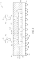
- FIG. 2 is a cross-sectional view taken along line I-I' of FIG. 1 .
- the semiconductor package 1 comprises a substrate 10 such as a packaging substrate or the like.
- the substrate 10 comprises a top surface (or chip-mounting surface) 10a and a bottom surface 10b.
- the traces and interconnection in the substrate 10 are not shown in the figures. It is understood that the substrate 10 comprises traces and interconnection elements that provide electrical connections between a chip and an external electronic component such as a system board.
- a plurality of solder balls 102 is disposed on the bottom surface 10b of the substrate 10.
- a semiconductor chip or die 20 may be mounted on the top surface 10a of the substrate 10 in a flip-chip fashion.
- the die 20 has an active surface 20a that faces downwardly to the substrate 10.
- a plurality of connecting elements 202 such as conductive bumps, micro bumps, pillars or the like may be provided on the active surface 20a.
- the connecting elements 202 are bonded to respective pads 104 disposed on the top surface 10a of the substrate 10.
- the die 20 may be underfilled with an encapsulant material 210 known in the art.
- an underfill resin with a coefficient of thermal expansion (CTE) close to that of the connecting elements 202 may be deposited and cured in a gap between the die 20 and substrate 10.
- CTE coefficient of thermal expansion
- a lid 30 is secured onto a perimeter of the top surface 10a of the substrate 10 with an adhesive layer 301.
- the lid 30 may comprise aluminum, copper or an alloy thereof, but is not limited thereto.
- a hermetic cavity 300 is created between the lid 30 and the substrate 10.
- the die 20 is disposed within the cavity 300 and housed by the lid 30.
- the lid 30 serves as physical protection for the die 20 as well as package stiffener to alleviate package warpage.
- the lid 30 comprises four walls 310 and a cover plate 312 formed integrally with the four walls 310.
- the four walls 310 are spaced apart from the die 20, while the cover plate 312 is directly secured to a rear surface 20b of the die 20 with an adhesive layer 302. It is understood that in some cases the cover plate 312 may be directly secured to the rear surface 20b of the die 20 with other means, for example, a solder tin coating.
- the lid 30 comprises a trenched feature 314 such as a serpentine half-etched trench recessed into a lower surface 312a of the cover plate 312.
- a liquid-cooling path or channel 320 for circulating a coolant 40 (shown in FIG. 1 ) relative to the semiconductor package 1 is formed between the cover plate 312 of the lid 30 and the rear surface 20b of the die 20.
- the liquid-cooling path or channel 320 is located only directly above the die 20 and does not extend beyond the die 20 when viewed from the above, as shown in FIG. 1 .
- the coolant 40 in the liquid-cooling path or channel 320 is in direct contact with the rear surface 20b of the die 20 during operation. Therefore, the heat generated from the die 20 can be efficiently dissipated by circulating the coolant 40 through the liquid-cooling path or channel 320 within the lid 30. Since a heat sink is spared, a very low profile semiconductor package can be provided. The improved semiconductor package is able to improve thermal performance without compromising the ability of warpage control and surface mount technique (SMT) control.
- SMT surface mount technique
- a liquid inlet 322 and a liquid outlet 324 may be provided in an upper surface 312b of the cover plate 312 of the lid 30.
- the liquid inlet 322 and the liquid outlet 324 communicate with the liquid-cooling path or channel 320, and may be situated at distal ends of the liquid-cooling path or channel 320, respectively.
- the liquid inlet 322 and the liquid outlet 324 are through holes with threaded inner surface.
- a conduit or pipe 50 with an end joint or an adaptor 512 may be provided to connect with either the liquid inlet 322 or the liquid outlet 324 for flowing coolant in or out of the upper surface 312b of the cover plate 312.
- the adaptor 512 may have a threaded outer surface configured for coupling the pipe 50 into the liquid inlet 322 or the liquid outlet 324 having a threaded inner surface. It is to be understood that the conduit or pipe 50 may be further connected to a pump (not shown).
- the liquid-cooling path or channel 320 may be composed of a plurality of manifolds 321.
- the liquid-cooling path or channel 320 may have a mesh-like pattern.
- FIG. 5 is a schematic, cross-sectional diagram showing a lidded semiconductor package in accordance with another embodiment of the invention.
- the differences between the semiconductor package 2 in FIG. 5 and the semiconductor package 1 in FIG. 2 include that the liquid inlet 322 and the liquid outlet 324 of the semiconductor package 2 in FIG. 5 are formed through the walls 310 and the cover plate 314 to provide a thinner semiconductor package.
- the arrangement of the liquid inlet 322 and the liquid outlet 324 in FIG. 5 is for illustration purposes only. It is to be understood that the liquid inlet 322 and the liquid outlet 324 may be provided on the same wall 310 or on different walls 310 of the lid 30.
- FIG. 6 is a perspective top view of a lidded semiconductor package in accordance with another embodiment of the invention.
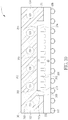
- FIG. 7 is a cross-sectional view taken along line II-II' of FIG. 6 .
- the semiconductor package 3 comprises a substrate 10 such as a packaging substrate or the like.
- the substrate 10 comprises a top surface 10a and a bottom surface 10b.
- a plurality of solder balls 102 may be disposed on the bottom surface 10b of the substrate 10.
- a die 20 may be mounted on the top surface 10a of the substrate 10 in a flip-chip fashion.
- the die 20 has an active surface 20a that faces downwardly to the substrate 10.
- a plurality of connecting elements 202 such as conductive bumps, micro bumps, pillars or the like may be provided on the active surface 20a.
- the connecting elements 202 are bonded to respective pads 104 disposed on the top surface 10a of the substrate 10.
- the die 20 may be underfilled with an encapsulant material 210 known in the art.
- an underfill resin with a CTE close to that of the connecting elements 202 may be deposited and cured in a gap between the die 20 and substrate 10.
- the lid 30 may comprise a liquid-cooling path or channel 320 for circulating a coolant 40 relative to the semiconductor package 3.
- the liquid-cooling path or channel 320 is buried in the lid 30, some portion of the liquid-cooling path or channel 320 may be located outside the projected area of the die 20 when viewed from the above.
- the coolant 40 in the liquid-cooling path or channel 320 is not in direct contact with the rear surface 20b of the die 20 during operation.
- a liquid inlet 322 and a liquid outlet 324 may be provided in an upper surface 312b of the cover plate 312 of the lid 30.
- the liquid inlet 322 and the liquid outlet 324 may be through holes with threaded inner surface.
- a conduit or pipe 50 with an end joint or an adaptor 512 may be provided to connect with either the liquid inlet 322 or the liquid outlet 324 for flowing coolant in or out of the upper surface 312b of the cover plate 312.
- the adaptor 512 may have a threaded outer surface configured for coupling the pipe 50 into the liquid inlet 322 or the liquid outlet 324 having a threaded inner surface.
- the liquid-cooling path or channel 320 may be composed of a plurality of manifolds 321.
- the liquid-cooling path or channel 320 may have a mesh-like pattern.
- some portions of the liquid-cooling path or channel 320 are located outside the projected area of the die 20 when viewed from the above.
- FIG. 10 is a schematic, cross-sectional diagram showing a lidded semiconductor package in accordance with another embodiment of the invention.
- the differences between the semiconductor package 4 in FIG. 10 and the semiconductor package 3 in FIG. 7 include that the liquid inlet 322 and the liquid outlet 324 of semiconductor package 4 in FIG. 10 are formed through the walls 310 to provide a thinner semiconductor package.
- the lateral arrangement of the liquid inlet 322 and the liquid outlet 324 in FIG. 10 is for illustration purposes only. It is to be understood that the liquid inlet 322 and the liquid outlet 324 may be provide on the same wall 310 or on different walls 310 of the lid 30.
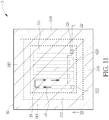
- FIG. 11 is a perspective top view of a lidded semiconductor package in accordance with yet another embodiment of the invention.
- FIG. 12 is a cross-sectional view taken along line III-III' of FIG. 11 .
- the semiconductor package 5 comprises a substrate 10 such as a packaging substrate or the like.
- the substrate 10 comprises a top surface 10a and a bottom surface 10b.
- the traces and interconnection in the substrate 10 are not shown in the figures.
- a plurality of solder balls 102 may be disposed on the bottom surface 10b of the substrate 10.
- a semiconductor chip or die 20 is mounted on the top surface 10a of the substrate 10 in a flip-chip fashion.
- the die 20 has an active surface 20a that faces downwardly to the substrate 10.
- a plurality of connecting elements 202 such as conductive bumps, micro bumps, pillars or the like may be provided on the active surface 20a.
- the connecting elements 202 are bonded to respective pads 104 disposed on the top surface 10a of the substrate 10.
- the die 20 may be underfilled with an encapsulant material 210 known in the art.
- the encapsulant material 210 surrounds the plurality of connecting elements 202.
- a lid 30 is secured onto a perimeter of the top surface 10a of the substrate 10 with an adhesive layer 301.
- the lid 30 may comprise aluminum, copper or an alloy thereof, but is not limited thereto.
- a cavity 300 is created between the lid 30 and the substrate 10 and the die 20 is disposed within the cavity 300.
- the lid 30 may comprise four walls 310 and a cover plate 312 formed integrally with the four walls 310. The four walls 310 are spaced apart from the die 20.
- a dummy layer 60 such as a dummy die or a dummy metal layer is provided between the lid 30 and the die 20.
- the dummy layer 60 has an upper surface 60a that is adhered to the lower surface 312a of the cover plate 312 of the lid 30 with an adhesive layer 602.
- the dummy layer 60 has a lower surface 60b that is adhered to the rear surface 20b of the die 20 with an adhesive layer 604.
- the dummy layer 60 comprises a trenched feature 614 such as a serpentine half-etched trench recessed into the upper surface 60a of the dummy layer 60.
- the lid 30 may have a thermal conductivity of about 300 W/(m ⁇ K) and the dummy layer 60 may have a thermal conductivity of at least about 180 W/(m-K).
- a liquid-cooling path or channel 620 for circulating a coolant 40 (shown in FIG. 11 ) relative to the semiconductor package 5 is formed between the cover plate 312 of the lid 30 and the dummy layer 60.
- the liquid-cooling path or channel 620 is located only directly above the die 20 when viewed from the above, as shown in FIG. 11 .
- the coolant 40 in the liquid-cooling path or channel 620 is not in direct contact with the rear surface 20b of the die 20 during operation.
- a liquid inlet 322 and a liquid outlet 324 may be provided in an upper surface 312b of the cover plate 312 of the lid 30.
- the liquid inlet 322 and the liquid outlet 324 may be through holes with threaded inner surface.
Landscapes
- Cooling Or The Like Of Semiconductors Or Solid State Devices (AREA)
Abstract
Description
- This application claims priority from
U.S. provisional application No. 62/896,028 filed on September 5, 2019 U.S. provisional application No. 62/991,618 filed on March 19, 2020 - The present disclosure relates generally to the field of semiconductor packaging. More particularly, the present disclosure relates to a lidded semiconductor package having a liquid-cooling lid mounted to back-side of a die without the need of applying a thermal interface material at an interface between the lid and die.
- Managing heat generated by the operating semiconductor chip has become an important technical issue. As temperature increases chip failure rates increase and heat may cause permanent damage to the semiconductor chip. Consequently, effective dissipation of heat becomes a crucial problem for semiconductor packages.
- Conventionally, a heat sink is attached to a surface of the semiconductor package to improve the heat dissipation. For example, in the case of a semiconductor package having a resin molding compound encapsulating the semiconductor chip, the heat sink is directly attached to a surface of the molding compound. Heat is transferred via the molding compound to the heat sink and the heat sink dissipates the heat via convection. However, the molding compound has a relatively low thermal conductivity and the efficiency of heat dissipation through the heat sink attached to the surface of the molding compound is relatively low.
- As power levels and heat generation increase in high-performance CPUs and other semiconductor devices, the thermal performance of commonly used packaging components is becoming a limiting factor. Many such devices are mounted in flip chip packages, in which the die is underfilled on the active side and in direct contact with a thermal interface material (also known as "TIM" or "TIM 1"), with a metal or ceramic lid attached on the opposite side. The lid serves as physical protection for the die as well as package stiffener, while the thermal interface material helps to dissipate excess heat. In some cases, a heat sink may be mounted on the lid with another TIM layer (also known as "TIM 2"). However, the thermal performance and heat-dissipating efficiency of the above-described configurations are still not satisfactory.
- With power levels steadily rising in new and emerging device designs, there is a constant need in this industry to provide improved thermal properties of semiconductor packages to ensure performance and reliability.
- It is an object of the invention to provide an improved semiconductor package with a liquid-cooling lid in order to solve the above-mentioned prior art problems or shortcomings.
- It is another object of the invention to provide an improved semiconductor package with improved thermal performance without compromising the ability of warpage control and surface mount technique (SMT) control.
- Semiconductor packages according to the invention are defined in the independent claims. The dependent claims define preferred embodiments thereof. One aspect of the invention provides a semiconductor package including a substrate, a die mounted on a top surface of the substrate in a flip-chip fashion, and a lid mounted on the die and on a perimeter of the substrate. The lid includes a cover plate and four walls formed integral with the cover plate. A liquid-cooling channel is situated between the cover plate of the lid and a rear surface of the die for circulating a coolant relative to the semiconductor package.
- Preferably, the cover plate is directly secured to the rear surface of the die with an adhesive layer.
- Preferably, the lid comprises a trenched feature recessed into a lower surface of the cover plate.
- Preferably, the trenched feature comprises a half-etched trench.
- Preferably, the liquid-cooling channel is constructed by combining the trenched feature and the rear surface of the die.
- Preferably, the coolant in the liquid-cooling channel is in direct contact with the rear surface of the die during operation.
- Preferably, the liquid-cooling channel is buried within the cover plate of the lid.
- Preferably, the coolant in the liquid-cooling channel is not in direct contact with the rear surface of the die during operation.
- Preferably, a liquid inlet and a liquid outlet are provided in the lid, which communicate with the liquid-cooling channel.
- Preferably, the liquid inlet and the liquid outlet are disposed in an upper surface of the cover plate.
- Preferably, the liquid inlet and the liquid outlet are disposed in at least one of the four walls.
- Preferably, the liquid inlet and the liquid outlet are through holes with threaded inner surface.
- Preferably, the die is underfilled with an encapsulant material.
- Preferably, a plurality of solder balls is disposed on a bottom surface of the substrate.
- Preferably, the substrate comprises a packaging substrate.
- Preferably, the lid comprises aluminum, copper or an alloy thereof.
- Another aspect of the invention provides a semiconductor package including a substrate; a die mounted on a top surface of the substrate in a flip-chip fashion, a dummy layer mounted on a rear surface of the die, and a lid mounted on the dummy layer and on a perimeter of the substrate. The lid includes a cover plate and four walls formed integral with the cover plate. A liquid-cooling channel is situated between the cover plate of the lid and the dummy layer for circulating a coolant relative to the semiconductor package.
- Preferably, the dummy layer comprises a dummy die or a metal layer.
- Preferably, the dummy layer has an upper surface that is adhered to a lower surface of the cover plate of the lid with a first adhesive layer
- Preferably, the dummy layer has a lower surface that is adhered to the rear surface of the die with a second adhesive layer.
- Preferably, the dummy layer comprises a trenched feature recessed into the upper surface of the dummy layer.
- These and other objectives of the present invention will no doubt become obvious to those of ordinary skill in the art after reading the following detailed description of the preferred embodiment that is illustrated in the various figures and drawings.
- The accompanying drawings are included to provide a further understanding of the invention and are incorporated in and constitute a part of this specification. The drawings illustrate embodiments of the invention and, together with the description, serve to explain the principles of the invention. In the drawings:
-
FIG. 1 is a perspective top view of a lidded semiconductor package in accordance with one embodiment of the invention; -
FIG. 2 is a cross-sectional view taken along line I-I' ofFIG. 1 ; -
FIG. 3 andFIG. 4 illustrate some exemplary patterns for the trenched feature in the lid according to various embodiments of the invention; -
FIG. 5 is a schematic, cross-sectional diagram showing a lidded semiconductor package in accordance with another embodiment of the invention; -
FIG. 6 is a perspective top view of a lidded semiconductor package in accordance with another embodiment of the invention; -
FIG. 7 is a cross-sectional view taken along line II-II' ofFIG. 6 ; -
FIG. 8 andFIG. 9 illustrate some exemplary patterns for the trenched feature in the lid according to various embodiments of the invention; -
FIG. 10 is a schematic, cross-sectional diagram showing a lidded semiconductor package in accordance with still another embodiment of the invention; -
FIG. 11 is a perspective top view of a lidded semiconductor package in accordance with yet another embodiment of the invention; and -
FIG. 12 is a cross-sectional view taken along line III-III' ofFIG. 11 . - In the following detailed description of embodiments of the invention, reference is made to the accompanying drawings, which form a part hereof, and in which is shown by way of illustration specific preferred embodiments in which the disclosure may be practiced.
- These embodiments are described in sufficient detail to enable those skilled in the art to practice them, and it is to be understood that other embodiments may be utilized and that mechanical, chemical, electrical, and procedural changes may be made without departing from the spirit and scope of the present disclosure. The following detailed description is, therefore, not to be taken in a limiting sense, and the scope of embodiments of the present invention is defined only by the appended claims.
- It will be understood that when an element or layer is referred to as being "on", "connected to" or "coupled to" another element or layer, it can be directly on, connected or coupled to the other element or layer or intervening elements or layers may be present. In contrast, when an element is referred to as being "directly on," "directly connected to" or "directly coupled to" another element or layer, there are no intervening elements or layers present. Like numbers refer to like elements throughout. As used herein, the term "and/or" includes any and all combinations of one or more of the associated listed items.
- Packaging of an integrated circuit (IC) chip can involve attaching the IC chip to a substrate (a packaging substrate) which, among other things, provides mechanical support and electrical connections between the chip and other electronic components of a device. Substrate types include, for example, cored substrates, including thin core, thick core (laminate BT (bismaleimide-triazine resin) or FR-4 type fibrous board material), and laminate core, as well as coreless substrates. Cored package substrates, for example, can be built up layer by layer around a central core, with layers of conductive material (usually copper) separated by layers of insulating dielectric, with interlayer connections being formed with through holes or microvias (vias).
- Thermal design and material selection continues to be a concern for electronic packages, particularly for flip chip ball grid array packages (FCBGA). Larger die sizes exhibit greater package warpage due to the difference in thermal expansion coefficients between silicon and laminate materials. As a result, large die packages are more difficult to solder mount and may produce larger variations in the bond line thickness between the die and external heat sinks.
- The present disclosure pertains to a flip chip lidded ball grid array (FCLBGA) package with a lid, such as a copper lid, mounted to the die back-side without the need of using a thermal interface material (also known as "
TIM 1") between the lid and die. The lid is integrated with at least one liquid-cooling path or liquid-cooling channel. Therefore, a conventional heat sink, which is usually mounted on the lid, may be spared. - Please refer to
FIG. 1 andFIG. 2 .FIG. 1 is a perspective top view of a lidded semiconductor package in accordance with one embodiment of the invention.FIG. 2 is a cross-sectional view taken along line I-I' ofFIG. 1 . As shown inFIG. 1 andFIG. 2 , thesemiconductor package 1 comprises asubstrate 10 such as a packaging substrate or the like. Thesubstrate 10 comprises a top surface (or chip-mounting surface) 10a and abottom surface 10b. For the sake of simplicity, the traces and interconnection in thesubstrate 10 are not shown in the figures. It is understood that thesubstrate 10 comprises traces and interconnection elements that provide electrical connections between a chip and an external electronic component such as a system board. - Preferably, a plurality of
solder balls 102 is disposed on thebottom surface 10b of thesubstrate 10. Preferably, a semiconductor chip or die 20 may be mounted on thetop surface 10a of thesubstrate 10 in a flip-chip fashion. Thedie 20 has anactive surface 20a that faces downwardly to thesubstrate 10. A plurality of connectingelements 202 such as conductive bumps, micro bumps, pillars or the like may be provided on theactive surface 20a. The connectingelements 202 are bonded torespective pads 104 disposed on thetop surface 10a of thesubstrate 10. The die 20 may be underfilled with anencapsulant material 210 known in the art. For example, an underfill resin with a coefficient of thermal expansion (CTE) close to that of the connectingelements 202 may be deposited and cured in a gap between the die 20 andsubstrate 10. The use of underfill resin enables structural coupling of the chip and substrate, effectively decreasing the shear stress and thus lowering the applied strain on the solder joints. - Preferably, a
lid 30 is secured onto a perimeter of thetop surface 10a of thesubstrate 10 with anadhesive layer 301. Preferably, thelid 30 may comprise aluminum, copper or an alloy thereof, but is not limited thereto. Ahermetic cavity 300 is created between thelid 30 and thesubstrate 10. Thedie 20 is disposed within thecavity 300 and housed by thelid 30. Thelid 30 serves as physical protection for the die 20 as well as package stiffener to alleviate package warpage. Preferably, thelid 30 comprises fourwalls 310 and acover plate 312 formed integrally with the fourwalls 310. The fourwalls 310 are spaced apart from thedie 20, while thecover plate 312 is directly secured to arear surface 20b of the die 20 with anadhesive layer 302. It is understood that in some cases thecover plate 312 may be directly secured to therear surface 20b of the die 20 with other means, for example, a solder tin coating. - Preferably, as can be seen in
FIG. 1 , thelid 30 comprises a trenchedfeature 314 such as a serpentine half-etched trench recessed into alower surface 312a of thecover plate 312. When thelid 30 is adhered onto thedie 20 and thesubstrate 10, a liquid-cooling path orchannel 320 for circulating a coolant 40 (shown inFIG. 1 ) relative to thesemiconductor package 1 is formed between thecover plate 312 of thelid 30 and therear surface 20b of thedie 20. Preferably, the liquid-cooling path orchannel 320 is located only directly above thedie 20 and does not extend beyond the die 20 when viewed from the above, as shown inFIG. 1 . - Preferably, the
coolant 40 in the liquid-cooling path orchannel 320 is in direct contact with therear surface 20b of the die 20 during operation. Therefore, the heat generated from the die 20 can be efficiently dissipated by circulating thecoolant 40 through the liquid-cooling path orchannel 320 within thelid 30. Since a heat sink is spared, a very low profile semiconductor package can be provided. The improved semiconductor package is able to improve thermal performance without compromising the ability of warpage control and surface mount technique (SMT) control. - Preferably, a
liquid inlet 322 and aliquid outlet 324 may be provided in anupper surface 312b of thecover plate 312 of thelid 30. Theliquid inlet 322 and theliquid outlet 324 communicate with the liquid-cooling path orchannel 320, and may be situated at distal ends of the liquid-cooling path orchannel 320, respectively. Preferably, as can be seen inFIG. 2 , theliquid inlet 322 and theliquid outlet 324 are through holes with threaded inner surface. A conduit orpipe 50 with an end joint or anadaptor 512 may be provided to connect with either theliquid inlet 322 or theliquid outlet 324 for flowing coolant in or out of theupper surface 312b of thecover plate 312. Preferably, theadaptor 512 may have a threaded outer surface configured for coupling thepipe 50 into theliquid inlet 322 or theliquid outlet 324 having a threaded inner surface. It is to be understood that the conduit orpipe 50 may be further connected to a pump (not shown). - Some exemplary patterns for the liquid-cooling path or
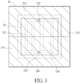
channel 320 are shown inFIG. 3 andFIG. 4 . For example, inFIG. 3 , the liquid-cooling path orchannel 320 may be composed of a plurality ofmanifolds 321. For example, inFIG. 4 , the liquid-cooling path orchannel 320 may have a mesh-like pattern. -
FIG. 5 is a schematic, cross-sectional diagram showing a lidded semiconductor package in accordance with another embodiment of the invention. As shown inFIG. 5 , the differences between thesemiconductor package 2 inFIG. 5 and thesemiconductor package 1 inFIG. 2 include that theliquid inlet 322 and theliquid outlet 324 of thesemiconductor package 2 inFIG. 5 are formed through thewalls 310 and thecover plate 314 to provide a thinner semiconductor package. It is to be understood that the arrangement of theliquid inlet 322 and theliquid outlet 324 inFIG. 5 is for illustration purposes only. It is to be understood that theliquid inlet 322 and theliquid outlet 324 may be provided on thesame wall 310 or ondifferent walls 310 of thelid 30. - Please refer to
FIG. 6 andFIG. 7 .FIG. 6 is a perspective top view of a lidded semiconductor package in accordance with another embodiment of the invention.FIG. 7 is a cross-sectional view taken along line II-II' ofFIG. 6 . Like layers, elements, or regions are designated by like numeral numbers or labels. As shown inFIG. 6 andFIG. 7 , likewise, thesemiconductor package 3 comprises asubstrate 10 such as a packaging substrate or the like. Thesubstrate 10 comprises atop surface 10a and abottom surface 10b. Preferably, a plurality ofsolder balls 102 may be disposed on thebottom surface 10b of thesubstrate 10. Preferably, adie 20 may be mounted on thetop surface 10a of thesubstrate 10 in a flip-chip fashion. Thedie 20 has anactive surface 20a that faces downwardly to thesubstrate 10. A plurality of connectingelements 202 such as conductive bumps, micro bumps, pillars or the like may be provided on theactive surface 20a. The connectingelements 202 are bonded torespective pads 104 disposed on thetop surface 10a of thesubstrate 10. The die 20 may be underfilled with anencapsulant material 210 known in the art. For example, an underfill resin with a CTE close to that of the connectingelements 202 may be deposited and cured in a gap between the die 20 andsubstrate 10. - Preferably, a
lid 30 is secured onto a perimeter of thetop surface 10a of thesubstrate 10 with anadhesive layer 301. Preferably, thelid 30 may comprise aluminum, copper or an alloy thereof, but is not limited thereto. Acavity 300 is created between thelid 30 and thesubstrate 10 and thedie 20 is disposed within thecavity 300. Preferably, thelid 30 comprises fourwalls 310 and acover plate 312 formed integrally with the fourwalls 310. The fourwalls 310 are spaced apart from thedie 20, while thecover plate 312 is directly secured to arear surface 20b of the die 20 with a thermal interface material (TIM)layer 303. For example, theTIM layer 303 may comprise low-modulus, Ag-filled or Al-filled gel or grease type TIM, but is not limited thereto. - Preferably, as can be seen in
FIG. 6 , thelid 30 may comprise a liquid-cooling path orchannel 320 for circulating acoolant 40 relative to thesemiconductor package 3. Preferably, sine the liquid-cooling path orchannel 320 is buried in thelid 30, some portion of the liquid-cooling path orchannel 320 may be located outside the projected area of the die 20 when viewed from the above. Preferably, thecoolant 40 in the liquid-cooling path orchannel 320 is not in direct contact with therear surface 20b of the die 20 during operation. - Preferably, a
liquid inlet 322 and aliquid outlet 324 may be provided in anupper surface 312b of thecover plate 312 of thelid 30. Preferably, as can be seen inFIG. 7 , theliquid inlet 322 and theliquid outlet 324 may be through holes with threaded inner surface. A conduit orpipe 50 with an end joint or anadaptor 512 may be provided to connect with either theliquid inlet 322 or theliquid outlet 324 for flowing coolant in or out of theupper surface 312b of thecover plate 312. Preferably, theadaptor 512 may have a threaded outer surface configured for coupling thepipe 50 into theliquid inlet 322 or theliquid outlet 324 having a threaded inner surface. - Some exemplary patterns for the liquid-cooling path or
channel 320 are shown inFIG. 8 andFIG. 9 . For example, inFIG. 8 , the liquid-cooling path orchannel 320 may be composed of a plurality ofmanifolds 321. For example, inFIG. 9 , the liquid-cooling path orchannel 320 may have a mesh-like pattern. InFIG. 8 andFIG. 9 , some portions of the liquid-cooling path orchannel 320 are located outside the projected area of the die 20 when viewed from the above. -
FIG. 10 is a schematic, cross-sectional diagram showing a lidded semiconductor package in accordance with another embodiment of the invention. As shown inFIG. 10 , the differences between thesemiconductor package 4 inFIG. 10 and thesemiconductor package 3 inFIG. 7 include that theliquid inlet 322 and theliquid outlet 324 ofsemiconductor package 4 inFIG. 10 are formed through thewalls 310 to provide a thinner semiconductor package. It is to be understood that the lateral arrangement of theliquid inlet 322 and theliquid outlet 324 inFIG. 10 is for illustration purposes only. It is to be understood that theliquid inlet 322 and theliquid outlet 324 may be provide on thesame wall 310 or ondifferent walls 310 of thelid 30. - Please refer to
FIG. 11 andFIG. 12 .FIG. 11 is a perspective top view of a lidded semiconductor package in accordance with yet another embodiment of the invention.FIG. 12 is a cross-sectional view taken along line III-III' ofFIG. 11 . Like layers, elements, or regions are designated by like numeral numbers or labels. As shown inFIG. 11 andFIG. 12 , likewise, the semiconductor package 5 comprises asubstrate 10 such as a packaging substrate or the like. Thesubstrate 10 comprises atop surface 10a and abottom surface 10b. For the sake of simplicity, the traces and interconnection in thesubstrate 10 are not shown in the figures. Preferably, a plurality ofsolder balls 102 may be disposed on thebottom surface 10b of thesubstrate 10. Preferably, a semiconductor chip or die 20 is mounted on thetop surface 10a of thesubstrate 10 in a flip-chip fashion. Thedie 20 has anactive surface 20a that faces downwardly to thesubstrate 10. A plurality of connectingelements 202 such as conductive bumps, micro bumps, pillars or the like may be provided on theactive surface 20a. The connectingelements 202 are bonded torespective pads 104 disposed on thetop surface 10a of thesubstrate 10. The die 20 may be underfilled with anencapsulant material 210 known in the art. Theencapsulant material 210 surrounds the plurality of connectingelements 202. - Preferably, a
lid 30 is secured onto a perimeter of thetop surface 10a of thesubstrate 10 with anadhesive layer 301. Preferably, thelid 30 may comprise aluminum, copper or an alloy thereof, but is not limited thereto. Acavity 300 is created between thelid 30 and thesubstrate 10 and thedie 20 is disposed within thecavity 300. Preferably, thelid 30 may comprise fourwalls 310 and acover plate 312 formed integrally with the fourwalls 310. The fourwalls 310 are spaced apart from thedie 20. - Preferably, as can be seen in
FIG. 12 , adummy layer 60 such as a dummy die or a dummy metal layer is provided between thelid 30 and thedie 20. Thedummy layer 60 has anupper surface 60a that is adhered to thelower surface 312a of thecover plate 312 of thelid 30 with anadhesive layer 602. Thedummy layer 60 has alower surface 60b that is adhered to therear surface 20b of the die 20 with anadhesive layer 604. Preferably, thedummy layer 60 comprises a trenched feature 614 such as a serpentine half-etched trench recessed into theupper surface 60a of thedummy layer 60. Preferably, for example, thelid 30 may have a thermal conductivity of about 300 W/(m·K) and thedummy layer 60 may have a thermal conductivity of at least about 180 W/(m-K). - As shown in
FIG. 11 andFIG. 12 , when thelid 30 is adhered onto thedummy layer 60 and thesubstrate 10, a liquid-cooling path orchannel 620 for circulating a coolant 40 (shown inFIG. 11 ) relative to the semiconductor package 5 is formed between thecover plate 312 of thelid 30 and thedummy layer 60. Preferably, the liquid-cooling path orchannel 620 is located only directly above the die 20 when viewed from the above, as shown inFIG. 11 . Preferably, thecoolant 40 in the liquid-cooling path orchannel 620 is not in direct contact with therear surface 20b of the die 20 during operation. Preferably, likewise, aliquid inlet 322 and aliquid outlet 324 may be provided in anupper surface 312b of thecover plate 312 of thelid 30. Preferably, as can be seen inFIG. 12 , theliquid inlet 322 and theliquid outlet 324 may be through holes with threaded inner surface. - Those skilled in the art will readily observe that numerous modifications and alterations of the device and method may be made while retaining the teachings of the invention. Accordingly, the above disclosure should be construed as limited only by the metes and bounds of the appended claims.
Claims (15)
- A semiconductor package (1; 2; 3; 4), comprising:a substrate (10);a die (20) mounted on a top surface (10a) of the substrate (10) in a flip-chip fashion;a lid (30) mounted on the die (20) and on a perimeter of the substrate (10), wherein the lid (30) comprises a cover plate (312) and four walls (310) formed integral with the cover plate (312); anda liquid-cooling channel (320) situated between the cover plate (312) of the lid (30) and a rear surface (20b) of the die (20) for circulating a coolant (40) relative to the semiconductor package (1; 2; 3; 4).
- The semiconductor package (1; 2; 3; 4) according to claim 1, wherein the cover plate (312) is directly secured to the rear surface (20b) of the die (20) with an adhesive layer (302).
- The semiconductor package (1; 2) according to claim 1 or 2, wherein the lid (30) comprises a trenched feature (314) recessed into a lower surface (312a) of the cover plate (312).
- The semiconductor package (1; 2) according to claim 3, wherein the trenched feature (314) comprises a half-etched trench; and/or
wherein the liquid-cooling channel (320) is constructed by combining the trenched feature (314) and the rear surface (20b) of the die (20); and/or
wherein the coolant (40) in the liquid-cooling channel (320) is in direct contact with the rear surface (20b) of the die (20) during operation. - The semiconductor package (3; 4) according to claim 1 or 2, wherein the liquid-cooling channel (320) is buried within the cover plate of the lid.
- The semiconductor package (3; 4) according to claim 5, wherein the coolant (40) in the liquid-cooling channel (320) is not in direct contact with the rear surface (20b) of the die (20) during operation.
- The semiconductor package (1; 2; 3; 4) according to any one of claims 1 to 6, wherein a liquid inlet (322) and a liquid outlet (324) are provided in the lid (30), which communicate with the liquid-cooling channel (320).
- The semiconductor package (1; 2; 3; 4) according to claim 7, wherein the liquid inlet (322) and/or the liquid outlet (324) are disposed in an upper surface (312b) of the cover plate (312) and/or in at least one of the four walls (310); and/or
wherein the liquid inlet (322) and the liquid outlet (324) are through holes with threaded inner surface. - The semiconductor package (1; 2; 3; 4) according to any one of claims 1 to 8, wherein the die (20) is underfilled with an encapsulant material (210).
- The semiconductor package (1; 2; 3; 4) according to any one of claims 1 to 9, wherein a plurality of solder balls (102) is disposed on a bottom surface (10b) of the substrate (10); and/or wherein the substrate (10) comprises a packaging substrate.
- The semiconductor package (1; 2; 3; 4) according to any one of claims 1 to 10, wherein the lid (30) comprises aluminum, copper or an alloy thereof.
- A semiconductor package (5), comprising:a substrate (10);a die (20) mounted on a top surface (10a) of the substrate (10) in a flip-chip fashion;a dummy layer (60) mounted on a rear surface (20b) of the die (20);a lid (30) mounted on the dummy layer (60) and on a perimeter of the substrate (10), wherein the lid (30) comprises a cover plate (312) and four walls (310) formed integral with the cover plate (312); anda liquid-cooling channel (620) situated between the cover plate (312) of the lid (30) and the dummy layer (60) for circulating a coolant (40) relative to the semiconductor package (5).
- The semiconductor package (5) according to claim 12, wherein the dummy layer (60) comprises a dummy die or a metal layer.
- The semiconductor package (5) according to claim 12 or 13, wherein the dummy layer (60) has an upper surface (60a) that is adhered to a lower surface (312a) of the cover plate (312) of the lid (30) with a first adhesive layer (602); and/or
wherein the dummy layer (60) has a lower surface (60b) that is adhered to the rear surface (20b) of the die (20) with a second adhesive layer (604). - The semiconductor package according to any one of claims 12 to 14, wherein the dummy layer (60) comprises a trenched feature (614) recessed into the upper surface (60a) of the dummy layer (60).
Applications Claiming Priority (3)
| Application Number | Priority Date | Filing Date | Title |
|---|---|---|---|
| US201962896028P | 2019-09-05 | 2019-09-05 | |
| US202062991618P | 2020-03-19 | 2020-03-19 | |
| US16/989,919 US11640930B2 (en) | 2019-09-05 | 2020-08-11 | Semiconductor package having liquid-cooling lid |
Publications (2)
| Publication Number | Publication Date |
|---|---|
| EP3792969A1 true EP3792969A1 (en) | 2021-03-17 |
| EP3792969B1 EP3792969B1 (en) | 2023-01-11 |
Family
ID=72193259
Family Applications (1)
| Application Number | Title | Priority Date | Filing Date |
|---|---|---|---|
| EP20191938.8A Active EP3792969B1 (en) | 2019-09-05 | 2020-08-20 | Semiconductor package having liquid-cooling lid |
Country Status (4)
| Country | Link |
|---|---|
| US (2) | US11640930B2 (en) |
| EP (1) | EP3792969B1 (en) |
| CN (1) | CN112447638A (en) |
| TW (1) | TWI742825B (en) |
Families Citing this family (7)
| Publication number | Priority date | Publication date | Assignee | Title |
|---|---|---|---|---|
| TWI898739B (en) * | 2020-05-29 | 2025-09-21 | 美商谷歌有限責任公司 | Methods and heat distribution devices for thermal management of chip assemblies, microelectronic device assembly, and method of assembling a cooling loop assembly to an in-process unit |
| US20220406686A1 (en) * | 2021-06-16 | 2022-12-22 | Intel Corporation | Glass-based cavity and channels for cooling of embedded dies and 3d integrated modules using package substrates with glass core |
| US20220406685A1 (en) * | 2021-06-16 | 2022-12-22 | Intel Corporation | 3d heterogeneously integrated systems with cooling channels in glass |
| US12622266B2 (en) * | 2021-11-23 | 2026-05-05 | Bae Systems Information And Electronic Systems Integration Inc. | Die level cavity heat sink |
| WO2023235342A1 (en) * | 2022-06-02 | 2023-12-07 | Ic Chip Cooling Technologies Llc | Lid with self sealing plug allowing for a thermal interface material with fluidity in a lidded flip chip package |
| CN117855172B (en) * | 2024-03-07 | 2024-05-17 | 江苏中科智芯集成科技有限公司 | An integrated chip heat dissipation channel and a processing technology of the heat dissipation channel |
| US12532432B2 (en) * | 2024-03-29 | 2026-01-20 | Adeia Semiconductor Bonding Technologies Inc. | Hotspot mitigation in fluid cooling |
Citations (7)
| Publication number | Priority date | Publication date | Assignee | Title |
|---|---|---|---|---|
| JPH04122054A (en) * | 1990-09-13 | 1992-04-22 | Hitachi Ltd | Semiconductor device |
| US6140141A (en) * | 1998-12-23 | 2000-10-31 | Sun Microsystems, Inc. | Method for cooling backside optically probed integrated circuits |
| US20030110788A1 (en) * | 2001-12-19 | 2003-06-19 | Koeneman Paul B. | Method and apparatus for cooling an integrated circuit package using a cooling fluid |
| EP1739746A2 (en) * | 2005-06-28 | 2007-01-03 | Delphi Technologies, Inc. | Fluid-cooled Electronic System |
| US20080230894A1 (en) * | 2007-03-21 | 2008-09-25 | Sun Microsystems, Inc. | Carbon nanotubes for active direct and indirect cooling of electronics device |
| US20090316360A1 (en) * | 2008-06-20 | 2009-12-24 | International Business Machines Corporation | Cooling apparatus and method of fabrication thereof with a cold plate formed in situ on a surface to be cooled |
| US20130148305A1 (en) * | 2011-12-08 | 2013-06-13 | Oracle International Corporation | Design of a heat dissipation structure for an integrated circuit (ic) chip |
Family Cites Families (5)
| Publication number | Priority date | Publication date | Assignee | Title |
|---|---|---|---|---|
| CA2070062C (en) | 1991-05-30 | 1997-01-07 | Hironobu Ikeda | Cooling structure for integrated circuits |
| US7633752B2 (en) * | 2004-03-29 | 2009-12-15 | Intel Corporation | Cooling an integrated circuit die with coolant flow in a microchannel and a thin film thermoelectric cooling device in the microchannel |
| US7394659B2 (en) | 2004-11-19 | 2008-07-01 | International Business Machines Corporation | Apparatus and methods for cooling semiconductor integrated circuit package structures |
| US20170186667A1 (en) | 2015-12-26 | 2017-06-29 | Intel Corporation | Cooling of electronics using folded foil microchannels |
| US11508645B2 (en) | 2017-09-29 | 2022-11-22 | Intel Corporation | Modular technique for die-level liquid cooling |
-
2020
- 2020-08-11 US US16/989,919 patent/US11640930B2/en active Active
- 2020-08-20 EP EP20191938.8A patent/EP3792969B1/en active Active
- 2020-08-26 CN CN202010871074.8A patent/CN112447638A/en active Pending
- 2020-08-28 TW TW109129570A patent/TWI742825B/en active
-
2023
- 2023-03-30 US US18/129,061 patent/US12087664B2/en active Active
Patent Citations (7)
| Publication number | Priority date | Publication date | Assignee | Title |
|---|---|---|---|---|
| JPH04122054A (en) * | 1990-09-13 | 1992-04-22 | Hitachi Ltd | Semiconductor device |
| US6140141A (en) * | 1998-12-23 | 2000-10-31 | Sun Microsystems, Inc. | Method for cooling backside optically probed integrated circuits |
| US20030110788A1 (en) * | 2001-12-19 | 2003-06-19 | Koeneman Paul B. | Method and apparatus for cooling an integrated circuit package using a cooling fluid |
| EP1739746A2 (en) * | 2005-06-28 | 2007-01-03 | Delphi Technologies, Inc. | Fluid-cooled Electronic System |
| US20080230894A1 (en) * | 2007-03-21 | 2008-09-25 | Sun Microsystems, Inc. | Carbon nanotubes for active direct and indirect cooling of electronics device |
| US20090316360A1 (en) * | 2008-06-20 | 2009-12-24 | International Business Machines Corporation | Cooling apparatus and method of fabrication thereof with a cold plate formed in situ on a surface to be cooled |
| US20130148305A1 (en) * | 2011-12-08 | 2013-06-13 | Oracle International Corporation | Design of a heat dissipation structure for an integrated circuit (ic) chip |
Also Published As
| Publication number | Publication date |
|---|---|
| TW202111889A (en) | 2021-03-16 |
| US12087664B2 (en) | 2024-09-10 |
| EP3792969B1 (en) | 2023-01-11 |
| TWI742825B (en) | 2021-10-11 |
| US20210074608A1 (en) | 2021-03-11 |
| US11640930B2 (en) | 2023-05-02 |
| US20230238302A1 (en) | 2023-07-27 |
| CN112447638A (en) | 2021-03-05 |
Similar Documents
| Publication | Publication Date | Title |
|---|---|---|
| CN213752684U (en) | Stacked silicon package assembly with vertical thermal management | |
| US12087664B2 (en) | Semiconductor package having liquid-cooling lid | |
| US12080614B2 (en) | Lidded semiconductor package | |
| US7190585B2 (en) | Thermal heat spreaders designed for lower cost manufacturability, lower mass and increased thermal performance | |
| TWI506743B (en) | Thermal management structure of semiconduvtor device and methods for forming the same | |
| US7135769B2 (en) | Semiconductor packages and methods of manufacturing thereof | |
| CA2676495C (en) | Mechanical barrier element for improved thermal reliability of electronic components | |
| KR102897692B1 (en) | Heat dissipation device having a thermally conductive structure and a thermal isolation structure in the thermally conductive structure | |
| US11101191B2 (en) | Laminated circuitry cooling for inter-chip bridges | |
| CN104882422A (en) | Stacked package structure | |
| CN104009016A (en) | Microelectronic package including an encapsulated heat spreade | |
| US20240371794A1 (en) | Semiconductor device and manufacturing method thereof | |
| CN105340078A (en) | Package-on-package structures | |
| CN115799229A (en) | Package for several integrated circuits | |
| US11984379B2 (en) | Electronic package and manufacturing method thereof | |
| CN103050455A (en) | Stack package structure | |
| EP4456128A1 (en) | Thermal management systems and methods for semiconductor devices | |
| US20240371721A1 (en) | Electronic package and manufacturing method thereof | |
| CN113906556A (en) | Chip packaging structure and circuit structure | |
| CN215451403U (en) | Semiconductor packaging structure | |
| TWI917962B (en) | Integrated circuit package assembly and method for forming the same | |
| TW202538992A (en) | Integrated circuit package assembly and method for forming the same | |
| CN119153418A (en) | Electronic package and method for manufacturing the same | |
| KR101234164B1 (en) | Semiconductor package having improved heat dissipation |
Legal Events
| Date | Code | Title | Description |
|---|---|---|---|
| PUAI | Public reference made under article 153(3) epc to a published international application that has entered the european phase |
Free format text: ORIGINAL CODE: 0009012 |
|
| STAA | Information on the status of an ep patent application or granted ep patent |
Free format text: STATUS: THE APPLICATION HAS BEEN PUBLISHED |
|
| AK | Designated contracting states |
Kind code of ref document: A1 Designated state(s): AL AT BE BG CH CY CZ DE DK EE ES FI FR GB GR HR HU IE IS IT LI LT LU LV MC MK MT NL NO PL PT RO RS SE SI SK SM TR |
|
| AX | Request for extension of the european patent |
Extension state: BA ME |
|
| STAA | Information on the status of an ep patent application or granted ep patent |
Free format text: STATUS: REQUEST FOR EXAMINATION WAS MADE |
|
| 17P | Request for examination filed |
Effective date: 20210917 |
|
| RBV | Designated contracting states (corrected) |
Designated state(s): AL AT BE BG CH CY CZ DE DK EE ES FI FR GB GR HR HU IE IS IT LI LT LU LV MC MK MT NL NO PL PT RO RS SE SI SK SM TR |
|
| GRAP | Despatch of communication of intention to grant a patent |
Free format text: ORIGINAL CODE: EPIDOSNIGR1 |
|
| STAA | Information on the status of an ep patent application or granted ep patent |
Free format text: STATUS: GRANT OF PATENT IS INTENDED |
|
| INTG | Intention to grant announced |
Effective date: 20220725 |
|
| GRAS | Grant fee paid |
Free format text: ORIGINAL CODE: EPIDOSNIGR3 |
|
| GRAA | (expected) grant |
Free format text: ORIGINAL CODE: 0009210 |
|
| STAA | Information on the status of an ep patent application or granted ep patent |
Free format text: STATUS: THE PATENT HAS BEEN GRANTED |
|
| AK | Designated contracting states |
Kind code of ref document: B1 Designated state(s): AL AT BE BG CH CY CZ DE DK EE ES FI FR GB GR HR HU IE IS IT LI LT LU LV MC MK MT NL NO PL PT RO RS SE SI SK SM TR |
|
| RAP3 | Party data changed (applicant data changed or rights of an application transferred) |
Owner name: MEDIATEK INC. |
|
| REG | Reference to a national code |
Ref country code: GB Ref legal event code: FG4D |
|
| RIN1 | Information on inventor provided before grant (corrected) |
Inventor name: YANG, BO-JIUN Inventor name: KUO, SHENG-LIANG Inventor name: CHEN, TAI-YU Inventor name: HSU, CHIA-HAO |
|
| REG | Reference to a national code |
Ref country code: DE Ref legal event code: R081 Ref document number: 602020007495 Country of ref document: DE Owner name: MEDIATEK INC., TW Free format text: FORMER OWNER: MEDIATEK INC., HSIN-CHU 300, TW |
|
| REG | Reference to a national code |
Ref country code: CH Ref legal event code: EP |
|
| REG | Reference to a national code |
Ref country code: DE Ref legal event code: R096 Ref document number: 602020007495 Country of ref document: DE |
|
| REG | Reference to a national code |
Ref country code: IE Ref legal event code: FG4D |
|
| REG | Reference to a national code |
Ref country code: AT Ref legal event code: REF Ref document number: 1543931 Country of ref document: AT Kind code of ref document: T Effective date: 20230215 |
|
| REG | Reference to a national code |
Ref country code: LT Ref legal event code: MG9D |
|
| REG | Reference to a national code |
Ref country code: NL Ref legal event code: MP Effective date: 20230111 |
|
| REG | Reference to a national code |
Ref country code: AT Ref legal event code: MK05 Ref document number: 1543931 Country of ref document: AT Kind code of ref document: T Effective date: 20230111 |
|
| PG25 | Lapsed in a contracting state [announced via postgrant information from national office to epo] |
Ref country code: NL Free format text: LAPSE BECAUSE OF FAILURE TO SUBMIT A TRANSLATION OF THE DESCRIPTION OR TO PAY THE FEE WITHIN THE PRESCRIBED TIME-LIMIT Effective date: 20230111 |
|
| P01 | Opt-out of the competence of the unified patent court (upc) registered |
Effective date: 20230607 |
|
| PG25 | Lapsed in a contracting state [announced via postgrant information from national office to epo] |
Ref country code: RS Free format text: LAPSE BECAUSE OF FAILURE TO SUBMIT A TRANSLATION OF THE DESCRIPTION OR TO PAY THE FEE WITHIN THE PRESCRIBED TIME-LIMIT Effective date: 20230111 Ref country code: PT Free format text: LAPSE BECAUSE OF FAILURE TO SUBMIT A TRANSLATION OF THE DESCRIPTION OR TO PAY THE FEE WITHIN THE PRESCRIBED TIME-LIMIT Effective date: 20230511 Ref country code: NO Free format text: LAPSE BECAUSE OF FAILURE TO SUBMIT A TRANSLATION OF THE DESCRIPTION OR TO PAY THE FEE WITHIN THE PRESCRIBED TIME-LIMIT Effective date: 20230411 Ref country code: LV Free format text: LAPSE BECAUSE OF FAILURE TO SUBMIT A TRANSLATION OF THE DESCRIPTION OR TO PAY THE FEE WITHIN THE PRESCRIBED TIME-LIMIT Effective date: 20230111 Ref country code: LT Free format text: LAPSE BECAUSE OF FAILURE TO SUBMIT A TRANSLATION OF THE DESCRIPTION OR TO PAY THE FEE WITHIN THE PRESCRIBED TIME-LIMIT Effective date: 20230111 Ref country code: HR Free format text: LAPSE BECAUSE OF FAILURE TO SUBMIT A TRANSLATION OF THE DESCRIPTION OR TO PAY THE FEE WITHIN THE PRESCRIBED TIME-LIMIT Effective date: 20230111 Ref country code: ES Free format text: LAPSE BECAUSE OF FAILURE TO SUBMIT A TRANSLATION OF THE DESCRIPTION OR TO PAY THE FEE WITHIN THE PRESCRIBED TIME-LIMIT Effective date: 20230111 Ref country code: AT Free format text: LAPSE BECAUSE OF FAILURE TO SUBMIT A TRANSLATION OF THE DESCRIPTION OR TO PAY THE FEE WITHIN THE PRESCRIBED TIME-LIMIT Effective date: 20230111 |
|
| PG25 | Lapsed in a contracting state [announced via postgrant information from national office to epo] |
Ref country code: SE Free format text: LAPSE BECAUSE OF FAILURE TO SUBMIT A TRANSLATION OF THE DESCRIPTION OR TO PAY THE FEE WITHIN THE PRESCRIBED TIME-LIMIT Effective date: 20230111 Ref country code: PL Free format text: LAPSE BECAUSE OF FAILURE TO SUBMIT A TRANSLATION OF THE DESCRIPTION OR TO PAY THE FEE WITHIN THE PRESCRIBED TIME-LIMIT Effective date: 20230111 Ref country code: IS Free format text: LAPSE BECAUSE OF FAILURE TO SUBMIT A TRANSLATION OF THE DESCRIPTION OR TO PAY THE FEE WITHIN THE PRESCRIBED TIME-LIMIT Effective date: 20230511 Ref country code: GR Free format text: LAPSE BECAUSE OF FAILURE TO SUBMIT A TRANSLATION OF THE DESCRIPTION OR TO PAY THE FEE WITHIN THE PRESCRIBED TIME-LIMIT Effective date: 20230412 Ref country code: FI Free format text: LAPSE BECAUSE OF FAILURE TO SUBMIT A TRANSLATION OF THE DESCRIPTION OR TO PAY THE FEE WITHIN THE PRESCRIBED TIME-LIMIT Effective date: 20230111 |
|
| REG | Reference to a national code |
Ref country code: DE Ref legal event code: R097 Ref document number: 602020007495 Country of ref document: DE |
|
| PG25 | Lapsed in a contracting state [announced via postgrant information from national office to epo] |
Ref country code: SM Free format text: LAPSE BECAUSE OF FAILURE TO SUBMIT A TRANSLATION OF THE DESCRIPTION OR TO PAY THE FEE WITHIN THE PRESCRIBED TIME-LIMIT Effective date: 20230111 Ref country code: RO Free format text: LAPSE BECAUSE OF FAILURE TO SUBMIT A TRANSLATION OF THE DESCRIPTION OR TO PAY THE FEE WITHIN THE PRESCRIBED TIME-LIMIT Effective date: 20230111 Ref country code: EE Free format text: LAPSE BECAUSE OF FAILURE TO SUBMIT A TRANSLATION OF THE DESCRIPTION OR TO PAY THE FEE WITHIN THE PRESCRIBED TIME-LIMIT Effective date: 20230111 Ref country code: DK Free format text: LAPSE BECAUSE OF FAILURE TO SUBMIT A TRANSLATION OF THE DESCRIPTION OR TO PAY THE FEE WITHIN THE PRESCRIBED TIME-LIMIT Effective date: 20230111 Ref country code: CZ Free format text: LAPSE BECAUSE OF FAILURE TO SUBMIT A TRANSLATION OF THE DESCRIPTION OR TO PAY THE FEE WITHIN THE PRESCRIBED TIME-LIMIT Effective date: 20230111 |
|
| PLBE | No opposition filed within time limit |
Free format text: ORIGINAL CODE: 0009261 |
|
| STAA | Information on the status of an ep patent application or granted ep patent |
Free format text: STATUS: NO OPPOSITION FILED WITHIN TIME LIMIT |
|
| PG25 | Lapsed in a contracting state [announced via postgrant information from national office to epo] |
Ref country code: SK Free format text: LAPSE BECAUSE OF FAILURE TO SUBMIT A TRANSLATION OF THE DESCRIPTION OR TO PAY THE FEE WITHIN THE PRESCRIBED TIME-LIMIT Effective date: 20230111 |
|
| 26N | No opposition filed |
Effective date: 20231012 |
|
| PG25 | Lapsed in a contracting state [announced via postgrant information from national office to epo] |
Ref country code: SI Free format text: LAPSE BECAUSE OF FAILURE TO SUBMIT A TRANSLATION OF THE DESCRIPTION OR TO PAY THE FEE WITHIN THE PRESCRIBED TIME-LIMIT Effective date: 20230111 |
|
| PG25 | Lapsed in a contracting state [announced via postgrant information from national office to epo] |
Ref country code: MC Free format text: LAPSE BECAUSE OF FAILURE TO SUBMIT A TRANSLATION OF THE DESCRIPTION OR TO PAY THE FEE WITHIN THE PRESCRIBED TIME-LIMIT Effective date: 20230111 |
|
| REG | Reference to a national code |
Ref country code: CH Ref legal event code: PL |
|
| PG25 | Lapsed in a contracting state [announced via postgrant information from national office to epo] |
Ref country code: MC Free format text: LAPSE BECAUSE OF FAILURE TO SUBMIT A TRANSLATION OF THE DESCRIPTION OR TO PAY THE FEE WITHIN THE PRESCRIBED TIME-LIMIT Effective date: 20230111 |
|
| PG25 | Lapsed in a contracting state [announced via postgrant information from national office to epo] |
Ref country code: LU Free format text: LAPSE BECAUSE OF NON-PAYMENT OF DUE FEES Effective date: 20230820 |
|
| PG25 | Lapsed in a contracting state [announced via postgrant information from national office to epo] |
Ref country code: LU Free format text: LAPSE BECAUSE OF NON-PAYMENT OF DUE FEES Effective date: 20230820 Ref country code: CH Free format text: LAPSE BECAUSE OF NON-PAYMENT OF DUE FEES Effective date: 20230831 |
|
| REG | Reference to a national code |
Ref country code: BE Ref legal event code: MM Effective date: 20230831 |
|
| REG | Reference to a national code |
Ref country code: IE Ref legal event code: MM4A |
|
| PG25 | Lapsed in a contracting state [announced via postgrant information from national office to epo] |
Ref country code: IT Free format text: LAPSE BECAUSE OF FAILURE TO SUBMIT A TRANSLATION OF THE DESCRIPTION OR TO PAY THE FEE WITHIN THE PRESCRIBED TIME-LIMIT Effective date: 20230111 |
|
| PG25 | Lapsed in a contracting state [announced via postgrant information from national office to epo] |
Ref country code: IE Free format text: LAPSE BECAUSE OF NON-PAYMENT OF DUE FEES Effective date: 20230820 |
|
| PG25 | Lapsed in a contracting state [announced via postgrant information from national office to epo] |
Ref country code: IE Free format text: LAPSE BECAUSE OF NON-PAYMENT OF DUE FEES Effective date: 20230820 |
|
| PG25 | Lapsed in a contracting state [announced via postgrant information from national office to epo] |
Ref country code: BE Free format text: LAPSE BECAUSE OF NON-PAYMENT OF DUE FEES Effective date: 20230831 |
|
| PG25 | Lapsed in a contracting state [announced via postgrant information from national office to epo] |
Ref country code: BG Free format text: LAPSE BECAUSE OF FAILURE TO SUBMIT A TRANSLATION OF THE DESCRIPTION OR TO PAY THE FEE WITHIN THE PRESCRIBED TIME-LIMIT Effective date: 20230111 |
|
| PG25 | Lapsed in a contracting state [announced via postgrant information from national office to epo] |
Ref country code: BG Free format text: LAPSE BECAUSE OF FAILURE TO SUBMIT A TRANSLATION OF THE DESCRIPTION OR TO PAY THE FEE WITHIN THE PRESCRIBED TIME-LIMIT Effective date: 20230111 |
|
| PGFP | Annual fee paid to national office [announced via postgrant information from national office to epo] |
Ref country code: GB Payment date: 20250626 Year of fee payment: 6 |
|
| PGFP | Annual fee paid to national office [announced via postgrant information from national office to epo] |
Ref country code: FR Payment date: 20250610 Year of fee payment: 6 |
|
| PG25 | Lapsed in a contracting state [announced via postgrant information from national office to epo] |
Ref country code: CY Free format text: LAPSE BECAUSE OF FAILURE TO SUBMIT A TRANSLATION OF THE DESCRIPTION OR TO PAY THE FEE WITHIN THE PRESCRIBED TIME-LIMIT; INVALID AB INITIO Effective date: 20200820 |
|
| PG25 | Lapsed in a contracting state [announced via postgrant information from national office to epo] |
Ref country code: HU Free format text: LAPSE BECAUSE OF FAILURE TO SUBMIT A TRANSLATION OF THE DESCRIPTION OR TO PAY THE FEE WITHIN THE PRESCRIBED TIME-LIMIT; INVALID AB INITIO Effective date: 20200820 |
|
| PGFP | Annual fee paid to national office [announced via postgrant information from national office to epo] |
Ref country code: DE Payment date: 20250624 Year of fee payment: 6 |
|
| REG | Reference to a national code |
Ref country code: DE Ref legal event code: R079 Ref document number: 602020007495 Country of ref document: DE Free format text: PREVIOUS MAIN CLASS: H01L0023473000 Ipc: H10W0040470000 |
|
| PG25 | Lapsed in a contracting state [announced via postgrant information from national office to epo] |
Ref country code: TR Free format text: LAPSE BECAUSE OF FAILURE TO SUBMIT A TRANSLATION OF THE DESCRIPTION OR TO PAY THE FEE WITHIN THE PRESCRIBED TIME-LIMIT Effective date: 20230111 |