EP3792622A1 - Interface unit for coupling a probe to a measuring system - Google Patents
Interface unit for coupling a probe to a measuring system Download PDFInfo
- Publication number
- EP3792622A1 EP3792622A1 EP19196402.2A EP19196402A EP3792622A1 EP 3792622 A1 EP3792622 A1 EP 3792622A1 EP 19196402 A EP19196402 A EP 19196402A EP 3792622 A1 EP3792622 A1 EP 3792622A1
- Authority
- EP
- European Patent Office
- Prior art keywords
- resistor
- transistor
- voltage
- terminal
- coupled
- Prior art date
- Legal status (The legal status is an assumption and is not a legal conclusion. Google has not performed a legal analysis and makes no representation as to the accuracy of the status listed.)
- Granted
Links
Images


Classifications
-
- G—PHYSICS
- G01—MEASURING; TESTING
- G01N—INVESTIGATING OR ANALYSING MATERIALS BY DETERMINING THEIR CHEMICAL OR PHYSICAL PROPERTIES
- G01N27/00—Investigating or analysing materials by the use of electric, electrochemical, or magnetic means
- G01N27/26—Investigating or analysing materials by the use of electric, electrochemical, or magnetic means by investigating electrochemical variables; by using electrolysis or electrophoresis
- G01N27/416—Systems
- G01N27/4161—Systems measuring the voltage and using a constant current supply, e.g. chronopotentiometry
-
- G—PHYSICS
- G01—MEASURING; TESTING
- G01R—MEASURING ELECTRIC VARIABLES; MEASURING MAGNETIC VARIABLES
- G01R1/00—Details of instruments or arrangements of the types included in groups G01R5/00 - G01R13/00 and G01R31/00
- G01R1/02—General constructional details
- G01R1/06—Measuring leads; Measuring probes
- G01R1/067—Measuring probes
- G01R1/06766—Input circuits therefor
-
- G—PHYSICS
- G01—MEASURING; TESTING
- G01R—MEASURING ELECTRIC VARIABLES; MEASURING MAGNETIC VARIABLES
- G01R31/00—Arrangements for testing electric properties; Arrangements for locating electric faults; Arrangements for electrical testing characterised by what is being tested not provided for elsewhere
- G01R31/28—Testing of electronic circuits, e.g. by signal tracer
- G01R31/2851—Testing of integrated circuits [IC]
- G01R31/2886—Features relating to contacting the IC under test, e.g. probe heads; chucks
- G01R31/2889—Interfaces, e.g. between probe and tester
-
- H—ELECTRICITY
- H03—ELECTRONIC CIRCUITRY
- H03K—PULSE TECHNIQUE
- H03K19/00—Logic circuits, i.e. having at least two inputs acting on one output; Inverting circuits
- H03K19/0175—Coupling arrangements; Interface arrangements
- H03K19/017509—Interface arrangements
- H03K19/017518—Interface arrangements using a combination of bipolar and field effect transistors [BIFET]
-
- G—PHYSICS
- G01—MEASURING; TESTING
- G01N—INVESTIGATING OR ANALYSING MATERIALS BY DETERMINING THEIR CHEMICAL OR PHYSICAL PROPERTIES
- G01N27/00—Investigating or analysing materials by the use of electric, electrochemical, or magnetic means
- G01N27/26—Investigating or analysing materials by the use of electric, electrochemical, or magnetic means by investigating electrochemical variables; by using electrolysis or electrophoresis
- G01N27/28—Electrolytic cell components
- G01N27/30—Electrodes, e.g. test electrodes; Half-cells
- G01N27/302—Electrodes, e.g. test electrodes; Half-cells pH sensitive, e.g. quinhydron, antimony or hydrogen electrodes
-
- G—PHYSICS
- G01—MEASURING; TESTING
- G01N—INVESTIGATING OR ANALYSING MATERIALS BY DETERMINING THEIR CHEMICAL OR PHYSICAL PROPERTIES
- G01N27/00—Investigating or analysing materials by the use of electric, electrochemical, or magnetic means
- G01N27/26—Investigating or analysing materials by the use of electric, electrochemical, or magnetic means by investigating electrochemical variables; by using electrolysis or electrophoresis
- G01N27/28—Electrolytic cell components
- G01N27/30—Electrodes, e.g. test electrodes; Half-cells
- G01N27/304—Gas permeable electrodes
-
- G—PHYSICS
- G01—MEASURING; TESTING
- G01N—INVESTIGATING OR ANALYSING MATERIALS BY DETERMINING THEIR CHEMICAL OR PHYSICAL PROPERTIES
- G01N27/00—Investigating or analysing materials by the use of electric, electrochemical, or magnetic means
- G01N27/26—Investigating or analysing materials by the use of electric, electrochemical, or magnetic means by investigating electrochemical variables; by using electrolysis or electrophoresis
- G01N27/28—Electrolytic cell components
- G01N27/30—Electrodes, e.g. test electrodes; Half-cells
- G01N27/307—Disposable laminated or multilayered electrodes
-
- G—PHYSICS
- G01—MEASURING; TESTING
- G01N—INVESTIGATING OR ANALYSING MATERIALS BY DETERMINING THEIR CHEMICAL OR PHYSICAL PROPERTIES
- G01N27/00—Investigating or analysing materials by the use of electric, electrochemical, or magnetic means
- G01N27/26—Investigating or analysing materials by the use of electric, electrochemical, or magnetic means by investigating electrochemical variables; by using electrolysis or electrophoresis
- G01N27/28—Electrolytic cell components
- G01N27/30—Electrodes, e.g. test electrodes; Half-cells
- G01N27/333—Ion-selective electrodes or membranes
-
- G—PHYSICS
- G01—MEASURING; TESTING
- G01N—INVESTIGATING OR ANALYSING MATERIALS BY DETERMINING THEIR CHEMICAL OR PHYSICAL PROPERTIES
- G01N27/00—Investigating or analysing materials by the use of electric, electrochemical, or magnetic means
- G01N27/26—Investigating or analysing materials by the use of electric, electrochemical, or magnetic means by investigating electrochemical variables; by using electrolysis or electrophoresis
- G01N27/28—Electrolytic cell components
- G01N27/30—Electrodes, e.g. test electrodes; Half-cells
- G01N27/36—Glass electrodes
-
- G—PHYSICS
- G01—MEASURING; TESTING
- G01R—MEASURING ELECTRIC VARIABLES; MEASURING MAGNETIC VARIABLES
- G01R1/00—Details of instruments or arrangements of the types included in groups G01R5/00 - G01R13/00 and G01R31/00
- G01R1/02—General constructional details
- G01R1/06—Measuring leads; Measuring probes
- G01R1/067—Measuring probes
- G01R1/06711—Probe needles; Cantilever beams; "Bump" contacts; Replaceable probe pins
- G01R1/06733—Geometry aspects
-
- G—PHYSICS
- G01—MEASURING; TESTING
- G01R—MEASURING ELECTRIC VARIABLES; MEASURING MAGNETIC VARIABLES
- G01R31/00—Arrangements for testing electric properties; Arrangements for locating electric faults; Arrangements for electrical testing characterised by what is being tested not provided for elsewhere
- G01R31/28—Testing of electronic circuits, e.g. by signal tracer
- G01R31/2801—Testing of printed circuits, backplanes, motherboards, hybrid circuits or carriers for multichip packages [MCP]
- G01R31/2806—Apparatus therefor, e.g. test stations, drivers, analysers, conveyors
- G01R31/2808—Holding, conveying or contacting devices, e.g. test adapters, edge connectors, extender boards
-
- G—PHYSICS
- G01—MEASURING; TESTING
- G01R—MEASURING ELECTRIC VARIABLES; MEASURING MAGNETIC VARIABLES
- G01R31/00—Arrangements for testing electric properties; Arrangements for locating electric faults; Arrangements for electrical testing characterised by what is being tested not provided for elsewhere
- G01R31/28—Testing of electronic circuits, e.g. by signal tracer
- G01R31/2851—Testing of integrated circuits [IC]
- G01R31/2855—Environmental, reliability or burn-in testing
- G01R31/286—External aspects, e.g. related to chambers, contacting devices or handlers
- G01R31/2863—Contacting devices, e.g. sockets, burn-in boards or mounting fixtures
-
- G—PHYSICS
- G01—MEASURING; TESTING
- G01R—MEASURING ELECTRIC VARIABLES; MEASURING MAGNETIC VARIABLES
- G01R31/00—Arrangements for testing electric properties; Arrangements for locating electric faults; Arrangements for electrical testing characterised by what is being tested not provided for elsewhere
- G01R31/28—Testing of electronic circuits, e.g. by signal tracer
- G01R31/2851—Testing of integrated circuits [IC]
- G01R31/2884—Testing of integrated circuits [IC] using dedicated test connectors, test elements or test circuits on the IC under test
-
- H—ELECTRICITY
- H03—ELECTRONIC CIRCUITRY
- H03F—AMPLIFIERS
- H03F3/00—Amplifiers with only discharge tubes or only semiconductor devices as amplifying elements
- H03F3/45—Differential amplifiers
- H03F3/45071—Differential amplifiers with semiconductor devices only
- H03F3/45076—Differential amplifiers with semiconductor devices only characterised by the way of implementation of the active amplifying circuit in the differential amplifier
- H03F3/45475—Differential amplifiers with semiconductor devices only characterised by the way of implementation of the active amplifying circuit in the differential amplifier using IC blocks as the active amplifying circuit
-
- H—ELECTRICITY
- H03—ELECTRONIC CIRCUITRY
- H03F—AMPLIFIERS
- H03F3/00—Amplifiers with only discharge tubes or only semiconductor devices as amplifying elements
- H03F3/50—Amplifiers in which input is applied to, or output is derived from, an impedance common to input and output circuits of the amplifying element, e.g. cathode follower
- H03F3/505—Amplifiers in which input is applied to, or output is derived from, an impedance common to input and output circuits of the amplifying element, e.g. cathode follower with field-effect devices
-
- G—PHYSICS
- G01—MEASURING; TESTING
- G01N—INVESTIGATING OR ANALYSING MATERIALS BY DETERMINING THEIR CHEMICAL OR PHYSICAL PROPERTIES
- G01N27/00—Investigating or analysing materials by the use of electric, electrochemical, or magnetic means
- G01N27/26—Investigating or analysing materials by the use of electric, electrochemical, or magnetic means by investigating electrochemical variables; by using electrolysis or electrophoresis
- G01N27/416—Systems
- G01N27/4166—Systems measuring a particular property of an electrolyte
- G01N27/4167—Systems measuring a particular property of an electrolyte pH
-
- G—PHYSICS
- G01—MEASURING; TESTING
- G01N—INVESTIGATING OR ANALYSING MATERIALS BY DETERMINING THEIR CHEMICAL OR PHYSICAL PROPERTIES
- G01N33/00—Investigating or analysing materials by specific methods not covered by groups G01N1/00 - G01N31/00
- G01N33/0004—Gaseous mixtures, e.g. polluted air
- G01N33/0009—General constructional details of gas analysers, e.g. portable test equipment
- G01N33/0027—General constructional details of gas analysers, e.g. portable test equipment concerning the detector
- G01N33/0036—General constructional details of gas analysers, e.g. portable test equipment concerning the detector specially adapted to detect a particular component
- G01N33/0039—O3
-
- G—PHYSICS
- G01—MEASURING; TESTING
- G01N—INVESTIGATING OR ANALYSING MATERIALS BY DETERMINING THEIR CHEMICAL OR PHYSICAL PROPERTIES
- G01N33/00—Investigating or analysing materials by specific methods not covered by groups G01N1/00 - G01N31/00
- G01N33/0004—Gaseous mixtures, e.g. polluted air
- G01N33/0009—General constructional details of gas analysers, e.g. portable test equipment
- G01N33/0027—General constructional details of gas analysers, e.g. portable test equipment concerning the detector
- G01N33/0036—General constructional details of gas analysers, e.g. portable test equipment concerning the detector specially adapted to detect a particular component
- G01N33/004—CO or CO2
-
- H—ELECTRICITY
- H03—ELECTRONIC CIRCUITRY
- H03F—AMPLIFIERS
- H03F2200/00—Indexing scheme relating to amplifiers
- H03F2200/261—Amplifier which being suitable for instrumentation applications
-
- H—ELECTRICITY
- H03—ELECTRONIC CIRCUITRY
- H03F—AMPLIFIERS
- H03F2200/00—Indexing scheme relating to amplifiers
- H03F2200/408—Indexing scheme relating to amplifiers the output amplifying stage of an amplifier comprising three power stages
-
- H—ELECTRICITY
- H03—ELECTRONIC CIRCUITRY
- H03F—AMPLIFIERS
- H03F2203/00—Indexing scheme relating to amplifiers with only discharge tubes or only semiconductor devices as amplifying elements covered by H03F3/00
- H03F2203/50—Indexing scheme relating to amplifiers in which input being applied to, or output being derived from, an impedance common to input and output circuits of the amplifying element, e.g. cathode follower
- H03F2203/5036—Indexing scheme relating to amplifiers in which input being applied to, or output being derived from, an impedance common to input and output circuits of the amplifying element, e.g. cathode follower the source follower has a resistor in its source circuit
Definitions
- the present disclosure relates to an interface unit for coupling the output on which a measuring probe delivers a voltage generated by an electrode, to an input of a measuring system for processing the voltage signal into measurements related to at least one property of a process material when the electrode is in contact with the process material.
- the interface unit and the corresponding method allows coupling, to a measuring system, measuring probes, such as for example an ion-sensitive measuring probe, in particular a pH-measuring probe, an oxygen-measuring probe, a CO 2 -measuring probe, or an ozone-measuring probe.
- measuring probes such as for example an ion-sensitive measuring probe, in particular a pH-measuring probe, an oxygen-measuring probe, a CO 2 -measuring probe, or an ozone-measuring probe.
- the monitoring and control of industrial processes is based on the measurement of process variables that are determined by means of suitable measuring probes.
- a complete measuring system consists of a housing, a measuring probe, a cable and a measurement converter (also called a transmitter).
- the measuring probe is brought into contact with the process that is to be measured or monitored, for example by immersing the probe in the process material and holding it there.
- the measuring probe serves to measure specific properties of the process.
- Measurement signals are sent through the cable to the transmitter, which communicates with a process control system and converts the measuring signals into readable data.
- the measuring probes are selected depending on the process material properties that are to be measured.
- the measuring probe is exposed to high temperature, commonly 140 °C and above.
- the measuring probe may be in contact with materials or products that should not be contaminated by infectious agents. Consequently, it is often necessary to sterilize the measuring probe using an autoclave.
- a measuring probe goes through the autoclaving process between 30 and up to 100 times.
- Measuring probes such as ion-sensitive measuring probes, typically carry a current through their sensing element, which is inherent to their functional principle. The higher the temperature the lower the resistance of the sensing element. For example, the glass resistance of the sensing element in a pH-measuring probe decreases drastically as the temperature reaches and exceeds 100 degrees Celsius.
- the impedance of the input stage circuit Under normal operations, when the input stage circuit is switched on, the impedance of the input stage circuit is at a high level. By contrast, when the input stage circuit is switched off and/or is in an unpowered state, the impedance of the input stage circuit falls to a low level, typically less than 1 kOhm.
- the input stage circuit is switched to zero current flow, which is often done during a high temperature process, the residual current rises between the sensing element and the input stage circuit, due to the low impedance of the operational amplifier, the input stage being in unpowered state. The current flowing through the sensor element increases drastically and may reach hazardous levels, causing very slow signal drifts and lasting damages to the sensor element.
- an improved interface unit for coupling the output voltage of a sensor element of a measuring probe - for example a potentiometric measuring probe such as an ion-sensitive measuring probe - to the input of the measuring system for processing said output voltage into measurements, the output voltage of the sensor element varying over a wide range of values - typically between 0.25 and 5.5 Volts - and in which current flowing through the sensor element is particularly low - typically inferior to 1 pA -, in particular when temperature reaches a high level - typically from 100 degrees Celsius - and/or when the input stage circuit is in an unpowered off state, especially if the sensing element is provided with an active voltage source, such as a solid-state pH sensor, while preserving the accuracy of the measurements affected negatively by the combination of high temperature and the lower impedance of the input stage circuit.
- an active voltage source such as a solid-state pH sensor
- the present invention concerns an interface unit comprising an input adapted to receive an input current having an input voltage, from an electrochemical measuring probe for use in contact with a process material.
- the electrochemical measuring probe comprises an electrode provided with a sensing element arranged so as to generate a sensor voltage.
- the electrode voltage is related to at least one property of the process material when the electrode is in contact with the process material.
- the electrochemical measuring probe is for example a potentiometric measuring probe. More particularly, the electrochemical measuring probe may be selected from the non-exhaustive group consisting of: a pH-measuring probe, an oxygen-measuring probe, a CO 2 -measuring probe, and an ozone-measuring probe.
- the impedance of the sensing element is for example sensibly comprised between 500 MOhms to 20 GOhms.
- the sensing element of the electrode may comprise an active layer behaving as a voltage source, the electrode voltage being not null even when the electrode is not in contact with the process material.
- the electrode may comprise a solid-state pH sensor comprising an active layer behaving as a voltage source.
- the electrode may comprise an ion pH-sensitive glass substrate and several layers on top of said ion pH-sensitive glass substrate.
- the layers may comprise an elementar/lithium layer, a Lithium Phosphorus Oxynitride - generally designed by the acronym LiPON - layer, and a protective layer adapted to limit degradations of the lithium layer as well as to provide a packaging structure for stabilizing the whole glass electrode against environmental influences.
- the electrical potential of the glass electrode of the measuring probe is not null, even when the glass electrode is not in contact with the process material.
- the interface unit further comprises an output adapted to be coupled to the input of an evaluating device.
- the evaluating device serves as measurement converters, and is coupled to a processing device, for example a computer.
- the input impedance of the evaluating device is low, for example sensibly comprised between 100 kOhms to 10 MOhms.
- the interface unit is arranged to deliver, on the output, an output current having an output voltage sensibly equal to the input voltage.
- an offset voltage between the input voltage and the output voltage of the interface unit may be sensibly inferior or equal to +/- 10 mV.
- the offset voltage remains sensibly constant under the normal range of temperatures reached at the sensor coupled to the interface unit - typically from sensibly 0 °C to 100 °C, regardless of the input voltage.
- the electrical specifications of the electrical components of the interface unit, and more particularly the tolerances of said electrical components, such as the tolerance of the nominal values of the resistors - are set so as that the tolerance for the difference between the output voltage of the interface unit and the input voltage is at least equal or better than +/- 0.1%.
- the offset voltage between the input voltage and the output voltage of the interface unit may be sensibly inferior or equal to +/- 2 mV.
- the offset voltage remains sensibly constant under the normal range of temperatures reached at the sensor coupled to the interface unit - typically from sensibly 0 °C to 100 °C, regardless of the input voltage.
- the interface unit may comprise means for adjusting the output voltage by compensating for the offset voltage. Since the offset voltage remains sensibly constant under the normal range of temperatures reached at the sensor coupled to the interface unit and regardless of the input voltage, a calibration step may be carried on once and stored in the interface unit. More particularly, the interface unit may be calibrated, after having been assembled. To that end, precisely measured and stable calibration signals may be applied as input voltage signals of the interface unit. The resulting output voltages of the interface unit are then measured: gain and offset values are then computed in order to compensate for discrepancies between the calibration signals and the output voltages, and may be stored in the interface unit, for example in an EEPROM controller. The gain and offset values may be accessed on demand, for example by a measuring software in order to compensate measurements values.
- the interfacing unit comprises a first transistor provided with a first insulated gate terminal coupled to the input, a first source terminal coupled to a first terminal of a first resistor, and a first drain terminal coupled to a first terminal of a second resistor.
- the second terminal of the first resistor being coupled to a point where a constant voltage is maintained to a constant value; the first transistor being arranged to generate in the second resistor a second resistor voltage, according to the input voltage.
- the interfacing unit comprises a first operational amplifier provided with a first non-inverting input coupled to a point of the circuit where a reference voltage is maintained to a constant value.
- the first operational amplifier is also provided with a first inverting input coupled to the first drain terminal of the first transistor.
- the first operational amplifier is also provided with a first output coupled to a second terminal of the first resistor.
- the interfacing unit further comprises a second transistor provided with a second source terminal coupled to a second terminal of a third resistor, and a second drain terminal coupled to a first terminal of a fourth resistor.
- the first terminal of the third resistor is coupled to the second terminal of the first resistor.
- the second terminal of the fourth resistor is coupled to a point where the constant voltage is maintained.
- the interfacing unit further comprises a second operational amplifier provided with a second non-inverting input coupled to the second drain terminal of the second transistor.
- the second operational amplifier is also provided with a second inverting input coupled to the first inverting input of the first operational amplifier.
- the second operational amplifier is also provided with a second output coupled a second insulated gate terminal of the second transistor and to the output of the interface unit.
- the first operational amplifier is arranged to provide a variable tension to the first source terminal of the first transistor, according to the comparison between the reference voltage and the second resistor voltage, in order to control the operating point of the first transistor.
- the interface unit is acting as an impedance buffer for transmitting a weak input signal received from a high impedance input to a low impedance output.
- the evaluating device is not directly fed by the electrode voltage itself nor an amplified voltage obtained directly by pre-amplifying the electrode voltage - as usually done in conventional input stage circuits, but by the decoupled voltage delivered by the interface unit.
- the electrode voltage is fed in the input through the first transistor through its insulated gate, provided a high insulation barrier.
- the interface unit provides an efficient current barrier, avoiding any significant load to be flowing through the input, and typically less than 1 pA. Consequently, the sensor element of the electrode is not charged anymore, thanks to the decoupling effect of the interface unit. Even at high temperatures - for example during an autoclaving process -, the influence of residual current on the sensor element of the electrode EL is kept exceptionally low. It provides an efficient solution to limit considerably negative effects on the electrode of residual currents, in particular when the measuring probe is switched to zero current flow, which is often done during a high temperature process.
- the interface unit By using transistors provided with insulated gate, the interface unit according to the invention allows to couple on the output signal-processing units having a conventional input stage circuit, including an Operational Amplifier.
- the interface unit according to the invention allows using an electrode comprising an active layer behaving as a voltage source, even in environment where temperature reaches and exceeds 100 degrees Celsius.
- electrodes with sensor elements comprising an elementar lithium layer it allows to drastically reduce the consumption of elementar lithium, and improve the life span of the probe. This is for example advantageous for solid-state pH sensors.
- the first operational amplifier is arranged to control the operating point - also known as Q-point or bias point - of the first transistor so as that the first transistor operates without saturation, distortion or other non-linear disturbances, for a wide range of values of the input voltage, typically between 0.25 and 5.5 Volts.
- the first operational amplifier remains at almost the same operating point, over a wide range of values of the input voltage.
- the gate of the first transistor is not linearly controlled in relation with the current flowing between the source and the drain of the first operational amplifier, maintaining a sensibly fixed operating point allows to increase the accuracy of the behaviour of the first operational amplifier, by reducing non-linear behaviour over a wide range of values for the input voltage V IN . In fine, the error introduced by the interface unit in the output voltage comparatively to the input voltage VIN is drastically reduced.
- the input voltage may vary only on a much more limited range of values for the input voltage compared to the invention, since saturation and/or distortion issues occur due to the fixed nature of the biasing current.
- the interface unit is arranged to compensate for discrepancies between electronic components - due to manufacturing tolerances for instance - by adapting the output voltage of the second operational amplifier accordingly.
- the first resistor may have a resistance sensibly identical to the resistance of the third resistor; and, the second resistor may have a resistance sensibly identical to the resistance of the third fourth resistor.
- the first transistor and the second transistor may also be of the same type.
- the same type of electronic component may be used for the first resistor and the third resistor.
- the same type of electronic component may be used for the first transistor and the second transistor.
- the same type of electronic component may be used for the first operational amplifier and the second operational amplifier.
- the interface unit then presents a balanced symmetrical design, providing an advantageous solution for reducing the cumulative influences on the interface unit of the variations of the environmental parameters - such as the variation of temperatures -, of the manufacturing tolerances for the electrical components, and of the electrical noises, can be greatly reduced, compared to circuits with a non-symmetrical design.
- the first operational amplifier and the second operational amplifier may be embedded in one package of a single electronic component.
- the first transistor and the second transistor may also be embedded in one package of a single electronic component.
- the first transistor and/or the second transistor may be chosen amongst the following list of types of transistors:
- the signal-processing unit may comprise an operational amplifier provided with an electrostatic discharge protection and configured so as to receive the decoupled voltage.
- the present invention also concerns a measuring system comprising:
- the sensing element of the electrode may comprise an active layer behaving as a voltage source, the electrode voltage being not null even when the electrode is not in contact with the process material.
- the measuring probe may be selected from the group consisting of: a pH-measuring probe, an oxygen-measuring probe, a CO 2 -measuring probe, and an ozone-measuring probe.
- the sensing element of the electrode may comprise a Lithium Phosphorus Oxynitride layer.
- FIG. 1 illustrates a measuring system with a container 8 comprising a holding vessel 81 filled with a process material 6.
- the properties of the process material 6 are measured by means of at least one electrochemical measuring probe 1 which are connected, through signal-transmitting device 2 to an interface unit 4.
- the interface unit 4 are also coupled to an evaluating device 3.
- the evaluating devices 3, which, among other functions, serve as measurement converters, is coupled to a processing device 500, for example a computer.
- the electrochemical measuring probe is for example a potentiometric measuring probe.
- the electrochemical measuring probe may be selected from the non-exhaustive group consisting of: a pH-measuring probe, an oxygen-measuring probe, a CO2-measuring probe, and an ozone-measuring probe.
- an electrochemical measuring probe such as for example a pH-measuring probe, which in the configuration of a single rod measuring chain includes a glass electrode 16, a reference electrode 15, and an auxiliary electrode 18, is represented schematically in FIG. 2 .
- the invention is not limited to a pH-measuring probe, and is also applicable to any type of electrochemical measuring probe, such as an oxygen-measuring probe, a CO 2 -measuring probe or an ozone-measuring probe.
- the glass electrode with a conductor lead element 16 and the reference electrode with a reference lead element 15 are constructively combined in one unit.
- the conductor lead element 16 is immersed in a solution with a defined pH value, specifically an inner buffer 14, which establishes the electrically conductive connection between the inside of the glass membrane 111 and the conductor lead element 16.
- the reference lead element 15 is immersed in an electrolyte, specifically an outer buffer 13 which, by way of a porous separating wall or diaphragm 121, allows an exchange of electrical charges to take place with the measurement material 6.
- the electrical potential at the conductor lead element 16, at the reference lead element 15, and/or at the auxiliary electrode 18 are intended to be measured and then further processed by the evaluating device 3 and the processing device 500.
- a temperature-measuring sensor 17 is arranged, which provides the possibility to automatically compensate for temperature effects and to register temperature cycles.
- the measuring probe 1 typically comprises an active layer behaving as a voltage source.
- the measuring probe 1 may be a solid-state pH sensor, the glass electrode 16 of the measuring probe 1 comprising typically an ion pH-sensitive glass substrate and several layers on top of said ion pH-sensitive glass substrate.
- the layers may comprise an elementar/lithium layer, a Lithium Phosphorus Oxynitride - generally designed by the acronym LiPON - layer, and a protective layer adapted to limit degradations of the lithium layer as well as to provide a packaging structure for stabilizing the whole glass electrode against environmental influences.
- the electrical potential of the glass electrode 16 of the measuring probe 1 is not null, even when the conductor lead element 16 is not immersed in the holding vessel 81 filled with the process material 6. This behaviour is notably due to the electrical characteristics of the elementar/lithium layer and the Lithium Phosphorus Oxynitride layer.
- FIG. 3 shows a circuit diagram of the interface unit 4 in an advantageous embodiment.
- Fig. 4 represents, for an exemplary input voltage signal, timing diagrams of various voltages - referenced hereafter in the description - measured in the circuit of the interface unit 4.
- the interface unit 4 comprises an input 110 adapted to receive an input voltage V IN .
- the input 110 is typically adapted to be coupled to an output of the measuring probe 1 which includes at least one electrode EL, for example a glass electrode and a reference electrode, so as to receive a sensor voltage V SENSOR .
- the sensor voltage V SENSOR may be observed either only when the measuring probe 1 is immersed in the process material 6 or constantly - in the case of use of a solid-state pH sensor, for example.
- the electrode EL itself forms a voltage source SQ.
- the input impedance Z in observed at the input 110 is particularly high, and typically superior to 2 GOhms, under usual operating temperatures of the sensor - typically from sensibly 0°C to 100 °C depending on the application. For instance, when the temperature of the sensor is around 25°C, the input impedance Z in observed at the input 110 is typically around 2.5 GOhms .
- the electrode resistance R E depends on the temperature observed at the measuring probe 1, the electrode resistance R E may become very small - typically inferior to 50 MOhms - above 100 degrees Celsius.
- the sensor voltage V SENSOR of the signal source SQ is not null, even when the conductor lead element 16 is not immersed in the holding vessel 81 - for example, the voltage observed at the glass electrode 16 is sensibly around -3V when the glass electrode is not in contact with the process material 6.
- the input 110 is typically electrically coupled to a test or calibration devices delivering a test signal.
- the interface unit 4 comprises an output 120 adapted notably to be electrically coupled to the input of the evaluating device 2.
- the interface unit 4 is configured to deliver on the output 120 an output voltage V OUT .
- the output impedance Z OUT observed at the output 120 is particularly low, and typically inferior to 100 Ohms.
- the interface unit 4 is arranged so as that the input voltage V IN observed at the input 110 is mirrored in the output 120, that is to say that, over time, the output voltage V OUT is maintained sensibly equal to the input voltage V IN .
- the difference between the input voltage and the output voltage is comprised between 0.1 mV and -0.4 mV for an input voltage varying from 0.25 V to 5.5 V.
- the interface unit 4 is also acting as an impedance buffer for transmitting a weak input signal received from a high impedance input to a low impedance output.
- the interface unit 4 is also providing a current barrier, avoiding any significant load to be flowing through the input 110, and typically less than 0.2 pA. Consequently, the sensor element of the electrode EL is not charged anymore, thanks to the interface unit 4. That's why, even at high temperatures - for example during an autoclaving process -, the influence of residual current on the sensor element of the electrode EL is kept exceptionally low. It provides an efficient solution to limit considerably negative effects on the electrode EL of residual currents, in particular when the measuring probe 1 is switched to zero current flow, which is often done during a high temperature process.
- the interface unit 4 further is provided with a decoupling circuit 200 and a potential mirroring circuit 300.
- the decoupling circuit 200 comprises a first transistor 210, a first operational amplifier 220, a first resistor 230 presenting a resistance R1 and a second resistor 240 presenting a resistance R2.
- the first transistor 210 is provided with an insulated gate terminal coupled to the input 110.
- the potential mirroring circuit 300 comprises a second transistor 310, a second operational amplifier 320, a third resistor 330 presenting a resistance R1, and a fourth resistor 340 presenting a resistance R4.
- the output 120 is coupled to an output of the second operational amplifier 320 and to an insulated gate terminal of the second transistor 310.
- the first transistor 210 also comprises a source terminal coupled to a first terminal of the first resistor 230, and a drain terminal coupled to a first terminal of the second resistor 240.
- a second terminal of the second resistor 240 is coupled to a point of the circuit where the voltage V C is maintained sensibly to a constant value, typically - 5.25 V.
- the first operational amplifier 220 is provided with a non-inverting input V+ coupled to a point of the circuit where the reference voltage V ref is maintained to a constant value, typically -5 V.
- the first operational amplifier 220 is also provided with an inverting input V- coupled to the drain terminal of the first transistor 210, to the first terminal of the second resistor 240, and to an inverting input V- of the second operational amplifier 320.
- the output of the operational amplifier 220 is coupled to a second terminal of the first resistor 230 and to a first terminal of the third resistor 330.
- the first operational amplifier 220 is arranged to provide a variable tension to the source terminal of the first transistor 210, according to the comparison between the reference voltage V ref received on its non-inverting input V+ and the voltage V R2 received on its inverting input V-.
- the first operational amplifier 220 is arranged to control the operating point - also known as Q-point or bias point - of the first transistor 210 so as that the first transistor 210 operates without saturation, distortion or other non-linear disturbances, for a wide range of values of the input voltage V IN , typically between 0.25 to 5.5 Volts.
- the first operational amplifier 220 remains at almost the same operating point, over a wide range of values of the input voltage V IN .
- the gate is not linearly controlled in relation with the current flowing between the source and the drain of the first operational amplifier 220, maintaining a sensibly fixed operating point allows to increase the accuracy of the behaviour of the first operational amplifier 220, by reducing non-linear behaviour over a wide range of values for the input voltage V IN .
- the error introduced by the interface unit in the output voltage VOUT comparatively to the input voltage VIN is drastically reduced, as illustrated for example in Figure 6.
- the input voltage may vary only on a much more limited range of values for the input voltage compared to the invention, since saturation and/or distortion issues occur due to the fixed nature of the biasing current.
- the second transistor 310 is provided with an insulated gate terminal coupled to the output of the second operational amplifier 320, a source terminal coupled to a second terminal of the third resistor 330, and a drain terminal coupled to a first terminal of the fourth resistor 240.
- a second terminal of the fourth resistor 340 is coupled to a point of the circuit where the voltage V C is maintained.
- the second operational amplifier 320 is provided with a non-inverting input V+ coupled to the drain terminal of the second transistor 310 and to the first terminal of the fourth resistor 340.
- the second operational amplifier 320 is also provided with an inverting input V- coupled to the inverting input V- of the first operational amplifier 320, to the first terminal of the second resistor 240 and to the drain terminal of the first transistor 210.
- the potential mirroring circuit 300 and the decoupling circuit 200 are sharing a balanced symmetrical design, in the sense that:
- the same type of electronic component may be used for the first resistor 230 and the third resistor R3.
- the same type of electronic component may be used for the first transistor 210 and the second transistor 310.
- the same type of electronic component may be used for the first operational amplifier 220 and the second operational amplifier 320. Since the potential mirroring circuit 300 and the decoupling circuit 200 are sharing a balanced symmetrical design, the cumulative influence on the interface unit 4 of the variations of the environmental parameters - such as the variation of temperatures -, of the manufacturing tolerances for the electrical components, and of the electrical noises, can be greatly reduced, compared to circuits with a non-symmetrical design.
- the first transistor 210 and/or the second transistor 310 is/are a Metal-Oxide-Semiconductor Field-Effect transistor (MOSFET), configured so as to adapt its conductivity ⁇ DEC according to its gate terminal.
- MOSFET Metal-Oxide-Semiconductor Field-Effect transistor
- the first transistor 210 and/or the second transistor 310 is/are an Insulated Gate Field-Effect transistor (IGFET).
- IGFET Insulated Gate Field-Effect transistor
- the first transistor 210 and/or the second transistor 310 are provided without an ElectroStatic-Discharge protecting element at gate. Consequently, the interface unit may be implemented using variety of different types of transistors, thereby giving more flexibility during the manufacturing process in allowing finding second sources of supply and optimizing costs.
- the first transistor 210 and/or the second transistor 310 is/are a Metal-Insulator-Semiconductor Field-Effect Transistor (MISFET).
- MISFET Metal-Insulator-Semiconductor Field-Effect Transistor
- the first transistor 210 and/or the second transistor 310 is/are is an Insulated-Gate Bipolar Transistor (IGBT).
- IGBT Insulated-Gate Bipolar Transistor
- the interface unit can be implemented using a large variety of different types of transistors, thereby offering more flexibility during the manufacturing process in allowing finding second sources of supply and/or optimizing costs.
- the first operational amplifier 220 and the second operational amplifier 320 are embedded in one package of a single electronic component, and/or the first transistor 210 and the second transistor 310 are embedded in one package of a single electronic component.
- the first transistor 210 is arranged to generate a decoupled voltage V R2 in the second resistor 240, according to the input voltage V IN received on the insulated gate terminal. More particularly, the decoupled voltage V R2 in the second resistor 240 is proportional to the current flowing in the first resistor 230 through the source to the gate of the first transistor 240 into the second resistor 240.
- V R2 in the second resistor 240 is proportional to the current flowing in the first resistor 230 through the source to the gate of the first transistor 240 into the second resistor 240.
- the output voltage V OUT delivered by the output terminal of the second operational amplifier 320 is controlling the gate of the second transistor 310 according to the voltage V C . Consequently, the second transistor 310 behaves similarly to the first transistor 210. Being arranged so as to replicate the behaviour of the first transistor 210, the second transistor 310 ensures symmetrical operations of the interface unit 4.
- the second transistor 310 is arranged to generate a voltage V R4 in the fourth resistor 340, according to the output voltage V OUT delivered by the output terminal of the second operational amplifier 320, received on the insulated gate terminal.
- the output 130 is also coupled to the insulated gate terminal of the second operational amplifier 320.
- the voltage V R4 in the fourth resistor 240 is proportional to the current flowing in the third resistor 330 through the source to the gate of the second transistor 310 into the fourth resistor 340.
Landscapes
- Physics & Mathematics (AREA)
- Engineering & Computer Science (AREA)
- General Physics & Mathematics (AREA)
- Life Sciences & Earth Sciences (AREA)
- Chemical & Material Sciences (AREA)
- Health & Medical Sciences (AREA)
- Computer Hardware Design (AREA)
- Pathology (AREA)
- Biochemistry (AREA)
- General Health & Medical Sciences (AREA)
- Analytical Chemistry (AREA)
- Immunology (AREA)
- Electrochemistry (AREA)
- Chemical Kinetics & Catalysis (AREA)
- Molecular Biology (AREA)
- General Engineering & Computer Science (AREA)
- Microelectronics & Electronic Packaging (AREA)
- Power Engineering (AREA)
- Geometry (AREA)
- Environmental & Geological Engineering (AREA)
- Computing Systems (AREA)
- Mathematical Physics (AREA)
- Investigating Or Analyzing Materials By The Use Of Electric Means (AREA)
- Semiconductor Integrated Circuits (AREA)
- Amplifiers (AREA)
Abstract
Description
- The present disclosure relates to an interface unit for coupling the output on which a measuring probe delivers a voltage generated by an electrode, to an input of a measuring system for processing the voltage signal into measurements related to at least one property of a process material when the electrode is in contact with the process material.
- More particularly, the interface unit and the corresponding method allows coupling, to a measuring system, measuring probes, such as for example an ion-sensitive measuring probe, in particular a pH-measuring probe, an oxygen-measuring probe, a CO2-measuring probe, or an ozone-measuring probe.
- The monitoring and control of industrial processes, for example in the chemical and pharmaceutical industries, in the textile industry, in the food and beverage industries, in the processing of paper and cellulose, or in the fields of water processing and waste water treatment, is based on the measurement of process variables that are determined by means of suitable measuring probes.
- According to "Process Measurement Solutions Catalog 2005/06", Mettler-Toledo GmbH, CH-8902 Urdorf, Switzerland, , a complete measuring system consists of a housing, a measuring probe, a cable and a measurement converter (also called a transmitter). By means of the housing, the measuring probe is brought into contact with the process that is to be measured or monitored, for example by immersing the probe in the process material and holding it there. The measuring probe serves to measure specific properties of the process. Measurement signals are sent through the cable to the transmitter, which communicates with a process control system and converts the measuring signals into readable data. The measuring probes are selected depending on the process material properties that are to be measured.
- It exists numerous situations in which the measuring probe is exposed to high temperature, commonly 140 °C and above. For example, in a pharmaceutical, medical or industrial food production context, the measuring probe may be in contact with materials or products that should not be contaminated by infectious agents. Consequently, it is often necessary to sterilize the measuring probe using an autoclave. In a typical use case, during its entire life span, a measuring probe goes through the autoclaving process between 30 and up to 100 times. Measuring probes, such as ion-sensitive measuring probes, typically carry a current through their sensing element, which is inherent to their functional principle. The higher the temperature the lower the resistance of the sensing element. For example, the glass resistance of the sensing element in a pH-measuring probe decreases drastically as the temperature reaches and exceeds 100 degrees Celsius.
- In order to amplify the voltage of the measuring signal to a suitable level, it is usual to couple the output of the sensing element of the measuring probe to an input stage circuit provided with an Operational Amplifier. Document
US 7 177 127 B2 , documentEP 2861975 B ,document EP 0 922 955 A2 and document Ryan Edwards: "Ion Selective Electrode Interface - Sparky's Widgets", 21 April 2017, as retrieved from the Internet URL https://www.sparkyswidgets.com/portfolio-item/ion-selective-electrode-interface/ on April 2018, disclose such kinds of solutions, for example. Under normal operations, when the input stage circuit is switched on, the impedance of the input stage circuit is at a high level. By contrast, when the input stage circuit is switched off and/or is in an unpowered state, the impedance of the input stage circuit falls to a low level, typically less than 1 kOhm. When the input stage circuit is switched to zero current flow, which is often done during a high temperature process, the residual current rises between the sensing element and the input stage circuit, due to the low impedance of the operational amplifier, the input stage being in unpowered state. The current flowing through the sensor element increases drastically and may reach hazardous levels, causing very slow signal drifts and lasting damages to the sensor element. - At high temperatures above 100 degrees Celsius, this issue is compounded by the sensible decrease of isolating characteristics of the semiconductors used in the Operational Amplifier for electrostatic discharge protection. In this context, the electrostatic discharge protection diode found in the Operational Amplifier may even cause short circuits.
- These issues are even more critical for sensing elements that are provided with an active voltage source, such as a solid-state pH sensor.
- A partial solution to connect an active sensing element to an input stage circuit of a measuring system while mitigating the above-mentioned current leakage issues, are known from the
patent document EP 1 010 249 B1 . However, these kinds of input stages do not allow to connect a probe delivering a sensing voltage varying according to a wide range of values - typically between 0.25 and 5.5 Volts- without introducing significant saturation and/or distortion issues into the output signal. Moreover, the known input stages are subject to electronic component manufacturing variation, introducing measurement errors. - That's why there is still a need for an improved interface unit for coupling the output voltage of a sensor element of a measuring probe - for example a potentiometric measuring probe such as an ion-sensitive measuring probe - to the input of the measuring system for processing said output voltage into measurements, the output voltage of the sensor element varying over a wide range of values - typically between 0.25 and 5.5 Volts - and in which current flowing through the sensor element is particularly low - typically inferior to 1 pA -, in particular when temperature reaches a high level - typically from 100 degrees Celsius - and/or when the input stage circuit is in an unpowered off state, especially if the sensing element is provided with an active voltage source, such as a solid-state pH sensor, while preserving the accuracy of the measurements affected negatively by the combination of high temperature and the lower impedance of the input stage circuit.
- To that end, according to a first aspect, the present invention concerns an interface unit comprising an input adapted to receive an input current having an input voltage, from an electrochemical measuring probe for use in contact with a process material.
- The electrochemical measuring probe comprises an electrode provided with a sensing element arranged so as to generate a sensor voltage. The electrode voltage is related to at least one property of the process material when the electrode is in contact with the process material.
- The electrochemical measuring probe is for example a potentiometric measuring probe. More particularly, the electrochemical measuring probe may be selected from the non-exhaustive group consisting of: a pH-measuring probe, an oxygen-measuring probe, a CO2-measuring probe, and an ozone-measuring probe.
- In typical operational conditions, according to the temperature, the impedance of the sensing element is for example sensibly comprised between 500 MOhms to 20 GOhms.
- The sensing element of the electrode may comprise an active layer behaving as a voltage source, the electrode voltage being not null even when the electrode is not in contact with the process material.
- For example, the electrode may comprise a solid-state pH sensor comprising an active layer behaving as a voltage source. The electrode may comprise an ion pH-sensitive glass substrate and several layers on top of said ion pH-sensitive glass substrate. The layers may comprise an elementar/lithium layer, a Lithium Phosphorus Oxynitride - generally designed by the acronym LiPON - layer, and a protective layer adapted to limit degradations of the lithium layer as well as to provide a packaging structure for stabilizing the whole glass electrode against environmental influences. The electrical potential of the glass electrode of the measuring probe is not null, even when the glass electrode is not in contact with the process material.
- The interface unit further comprises an output adapted to be coupled to the input of an evaluating device. For example, the evaluating device serves as measurement converters, and is coupled to a processing device, for example a computer. In typical operational conditions, the input impedance of the evaluating device is low, for example sensibly comprised between 100 kOhms to 10 MOhms.
- The interface unit is arranged to deliver, on the output, an output current having an output voltage sensibly equal to the input voltage. For example, an offset voltage between the input voltage and the output voltage of the interface unit may be sensibly inferior or equal to +/- 10 mV. The offset voltage remains sensibly constant under the normal range of temperatures reached at the sensor coupled to the interface unit - typically from sensibly 0 °C to 100 °C, regardless of the input voltage.
- In an advantageous embodiment, the electrical specifications of the electrical components of the interface unit, and more particularly the tolerances of said electrical components, such as the tolerance of the nominal values of the resistors - are set so as that the tolerance for the difference between the output voltage of the interface unit and the input voltage is at least equal or better than +/- 0.1%. Accordingly, the offset voltage between the input voltage and the output voltage of the interface unit may be sensibly inferior or equal to +/- 2 mV. The offset voltage remains sensibly constant under the normal range of temperatures reached at the sensor coupled to the interface unit - typically from sensibly 0 °C to 100 °C, regardless of the input voltage.
- Advantageously, the interface unit may comprise means for adjusting the output voltage by compensating for the offset voltage. Since the offset voltage remains sensibly constant under the normal range of temperatures reached at the sensor coupled to the interface unit and regardless of the input voltage, a calibration step may be carried on once and stored in the interface unit. More particularly, the interface unit may be calibrated, after having been assembled. To that end, precisely measured and stable calibration signals may be applied as input voltage signals of the interface unit. The resulting output voltages of the interface unit are then measured: gain and offset values are then computed in order to compensate for discrepancies between the calibration signals and the output voltages, and may be stored in the interface unit, for example in an EEPROM controller. The gain and offset values may be accessed on demand, for example by a measuring software in order to compensate measurements values.
- The interfacing unit comprises a first transistor provided with a first insulated gate terminal coupled to the input, a first source terminal coupled to a first terminal of a first resistor, and a first drain terminal coupled to a first terminal of a second resistor. The second terminal of the first resistor being coupled to a point where a constant voltage is maintained to a constant value; the first transistor being arranged to generate in the second resistor a second resistor voltage, according to the input voltage.
- The interfacing unit comprises a first operational amplifier provided with a first non-inverting input coupled to a point of the circuit where a reference voltage is maintained to a constant value. The first operational amplifier is also provided with a first inverting input coupled to the first drain terminal of the first transistor. The first operational amplifier is also provided with a first output coupled to a second terminal of the first resistor.
- The interfacing unit further comprises a second transistor provided with a second source terminal coupled to a second terminal of a third resistor, and a second drain terminal coupled to a first terminal of a fourth resistor. The first terminal of the third resistor is coupled to the second terminal of the first resistor. The second terminal of the fourth resistor is coupled to a point where the constant voltage is maintained.
- The interfacing unit further comprises a second operational amplifier provided with a second non-inverting input coupled to the second drain terminal of the second transistor. The second operational amplifier is also provided with a second inverting input coupled to the first inverting input of the first operational amplifier. The second operational amplifier is also provided with a second output coupled a second insulated gate terminal of the second transistor and to the output of the interface unit.
- The first operational amplifier is arranged to provide a variable tension to the first source terminal of the first transistor, according to the comparison between the reference voltage and the second resistor voltage, in order to control the operating point of the first transistor.
- The interface unit is acting as an impedance buffer for transmitting a weak input signal received from a high impedance input to a low impedance output.
- According to the invention, the evaluating device is not directly fed by the electrode voltage itself nor an amplified voltage obtained directly by pre-amplifying the electrode voltage - as usually done in conventional input stage circuits, but by the decoupled voltage delivered by the interface unit. Moreover, the electrode voltage is fed in the input through the first transistor through its insulated gate, provided a high insulation barrier. The interface unit provides an efficient current barrier, avoiding any significant load to be flowing through the input, and typically less than 1 pA. Consequently, the sensor element of the electrode is not charged anymore, thanks to the decoupling effect of the interface unit. Even at high temperatures - for example during an autoclaving process -, the influence of residual current on the sensor element of the electrode EL is kept exceptionally low. It provides an efficient solution to limit considerably negative effects on the electrode of residual currents, in particular when the measuring probe is switched to zero current flow, which is often done during a high temperature process.
- By using transistors provided with insulated gate, the interface unit according to the invention allows to couple on the output signal-processing units having a conventional input stage circuit, including an Operational Amplifier.
- Moreover, since the influence of residual current on the sensor element of the electrode EL is drastically reduced by the action of the transistor with the insulated gate, the interface unit according to the invention allows using an electrode comprising an active layer behaving as a voltage source, even in environment where temperature reaches and exceeds 100 degrees Celsius. For electrodes with sensor elements comprising an elementar lithium layer, it allows to drastically reduce the consumption of elementar lithium, and improve the life span of the probe. This is for example advantageous for solid-state pH sensors.
- The first operational amplifier is arranged to control the operating point - also known as Q-point or bias point - of the first transistor so as that the first transistor operates without saturation, distortion or other non-linear disturbances, for a wide range of values of the input voltage, typically between 0.25 and 5.5 Volts. The first operational amplifier remains at almost the same operating point, over a wide range of values of the input voltage. Moreover, since the gate of the first transistor is not linearly controlled in relation with the current flowing between the source and the drain of the first operational amplifier, maintaining a sensibly fixed operating point allows to increase the accuracy of the behaviour of the first operational amplifier, by reducing non-linear behaviour over a wide range of values for the input voltage VIN. In fine, the error introduced by the interface unit in the output voltage comparatively to the input voltage VIN is drastically reduced.
- By contrast, in known solutions where a steady-state DC voltage or constant current is applied for biasing the source of the transistor, the input voltage may vary only on a much more limited range of values for the input voltage compared to the invention, since saturation and/or distortion issues occur due to the fixed nature of the biasing current.
- Moreover, by coupling the inverting input of the second operational amplifier to the inverting input of the first operational amplifier, the interface unit is arranged to compensate for discrepancies between electronic components - due to manufacturing tolerances for instance - by adapting the output voltage of the second operational amplifier accordingly.
- Advantageously, the first resistor may have a resistance sensibly identical to the resistance of the third resistor; and, the second resistor may have a resistance sensibly identical to the resistance of the third fourth resistor. The first transistor and the second transistor may also be of the same type.
- In particular, the same type of electronic component may be used for the first resistor and the third resistor. The same type of electronic component may be used for the first transistor and the second transistor. The same type of electronic component may be used for the first operational amplifier and the second operational amplifier. The interface unit then presents a balanced symmetrical design, providing an advantageous solution for reducing the cumulative influences on the interface unit of the variations of the environmental parameters - such as the variation of temperatures -, of the manufacturing tolerances for the electrical components, and of the electrical noises, can be greatly reduced, compared to circuits with a non-symmetrical design.
- Advantageously, the first operational amplifier and the second operational amplifier may be embedded in one package of a single electronic component. The first transistor and the second transistor may also be embedded in one package of a single electronic component. These features allow to further improve the reduction of the influence of the variations of the environmental parameters, of the manufacturing tolerances for the electrical components, and of the electrical noises. Moreover, the footprint of the interface unit may be further reduced, while the production cost may be lowered.
- More particularly, the first transistor and/or the second transistor may be chosen amongst the following list of types of transistors:
- an Insulated Gate Field-Effect transistor (IGFET), without ElectroStatic-Discharge protecting element at gate ; or
- a Metal-Oxide-Semiconductor Field-Effect Transistor (MOSFET), providing a particularly efficient insulation barrier on the gate, and being adapted to be used under environments where temperature may vary broadly, and exceeds 100 degrees Celsius, since an oxide layer is used between the gate and the channel of the MOSFET, to prevent current from flowing within a wide temperature range; or,
- a Metal-Insulator-Semiconductor Field-Effect Transistor (MISFET); or
- an Insulated-Gate Bipolar Transistor (IGBT).
- The signal-processing unit may comprise an operational amplifier provided with an electrostatic discharge protection and configured so as to receive the decoupled voltage. As a consequence, it is possible to use a conventional input stage circuit, having standard electrostatic discharge protection, and then, use proven reliable signal-processing unit, without requiring any costly re-engineering and/or tailored made solutions.
- According to a second aspect, the present invention also concerns a measuring system comprising:
- an interface unit according to the first aspect; and,
- an electrochemical measuring probe for use in contact with a process material, comprising an electrode provided with a sensing element arranged so as to generate a sensor voltage, the electrode voltage being related to at least one property of the process material when the electrode is in contact with the process material; the electrochemical measuring probe being adapted to deliver the sensor voltage to the input of the interface unit;
- an evaluating device provided with an input adapted to be coupled to the output of the interface unit, for receiving the output voltage, for converting the output voltage into measurements.
- The sensing element of the electrode may comprise an active layer behaving as a voltage source, the electrode voltage being not null even when the electrode is not in contact with the process material.
- The measuring probe may be selected from the group consisting of: a pH-measuring probe, an oxygen-measuring probe, a CO2-measuring probe, and an ozone-measuring probe.
- The sensing element of the electrode may comprise a Lithium Phosphorus Oxynitride layer.
- Details of the disclosed method and device will become apparent from the description of the embodiments which are shown in schematic and simplified representation in the drawings, wherein:
- Fig. 1
- illustrates the principal structure of a system for measuring at least one property of a
process material 6 by means of a measuringprobe 1; - Fig. 2
- schematically illustrates an
electrochemical measuring probe 1 which is immersed in aprocess material 6 and coupled to an evaluatingdevice 3; - Fig. 3
- represents a schematic circuit diagram of the
interface unit 4 ; - Fig. 4
- represents timing diagrams of various voltage measured in the circuit of the
interface unit 4, for an example of an input voltage signal; - Fig. 5
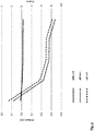
- represents an error diagram where the offset voltage diff. mV between the input voltage and the output voltage of the interface unit and the related measurement errors are represented over time - abscissa representing time in milliseconds.
-
FIG. 1 illustrates a measuring system with acontainer 8 comprising a holdingvessel 81 filled with aprocess material 6. The properties of theprocess material 6 are measured by means of at least oneelectrochemical measuring probe 1 which are connected, through signal-transmittingdevice 2 to aninterface unit 4. Theinterface unit 4 are also coupled to an evaluatingdevice 3. The evaluatingdevices 3, which, among other functions, serve as measurement converters, is coupled to aprocessing device 500, for example a computer. The electrochemical measuring probe is for example a potentiometric measuring probe. More particularly, the electrochemical measuring probe may be selected from the non-exhaustive group consisting of: a pH-measuring probe, an oxygen-measuring probe, a CO2-measuring probe, and an ozone-measuring probe. - The principal design structure of an electrochemical measuring probe such as for example a pH-measuring probe, which in the configuration of a single rod measuring chain includes a
glass electrode 16, areference electrode 15, and anauxiliary electrode 18, is represented schematically inFIG. 2 . However, the invention is not limited to a pH-measuring probe, and is also applicable to any type of electrochemical measuring probe, such as an oxygen-measuring probe, a CO2-measuring probe or an ozone-measuring probe. - In the measuring
probe 1, the glass electrode with aconductor lead element 16 and the reference electrode with areference lead element 15 are constructively combined in one unit. Inside a first chamber within aninner tube 11 and a thin-walled glass hemisphere orglass membrane 111 adjoining the tube, theconductor lead element 16 is immersed in a solution with a defined pH value, specifically aninner buffer 14, which establishes the electrically conductive connection between the inside of theglass membrane 111 and theconductor lead element 16. Inside anouter tube 12, thereference lead element 15 is immersed in an electrolyte, specifically anouter buffer 13 which, by way of a porous separating wall ordiaphragm 121, allows an exchange of electrical charges to take place with themeasurement material 6. - The electrical potential at the
conductor lead element 16, at thereference lead element 15, and/or at theauxiliary electrode 18 are intended to be measured and then further processed by the evaluatingdevice 3 and theprocessing device 500. - In the inner buffer space, a temperature-measuring
sensor 17 is arranged, which provides the possibility to automatically compensate for temperature effects and to register temperature cycles. - The measuring
probe 1 typically comprises an active layer behaving as a voltage source. For example, the measuringprobe 1 may be a solid-state pH sensor, theglass electrode 16 of the measuringprobe 1 comprising typically an ion pH-sensitive glass substrate and several layers on top of said ion pH-sensitive glass substrate. The layers may comprise an elementar/lithium layer, a Lithium Phosphorus Oxynitride - generally designed by the acronym LiPON - layer, and a protective layer adapted to limit degradations of the lithium layer as well as to provide a packaging structure for stabilizing the whole glass electrode against environmental influences. The electrical potential of theglass electrode 16 of the measuringprobe 1 is not null, even when theconductor lead element 16 is not immersed in the holdingvessel 81 filled with theprocess material 6. This behaviour is notably due to the electrical characteristics of the elementar/lithium layer and the Lithium Phosphorus Oxynitride layer. -
FIG. 3 shows a circuit diagram of theinterface unit 4 in an advantageous embodiment.Fig. 4 represents, for an exemplary input voltage signal, timing diagrams of various voltages - referenced hereafter in the description - measured in the circuit of theinterface unit 4. Theinterface unit 4 comprises aninput 110 adapted to receive an input voltage VIN. Theinput 110 is typically adapted to be coupled to an output of the measuringprobe 1 which includes at least one electrode EL, for example a glass electrode and a reference electrode, so as to receive a sensor voltage VSENSOR. Depending on the type of the measuringprobe 1 used, the sensor voltage VSENSOR may be observed either only when the measuringprobe 1 is immersed in theprocess material 6 or constantly - in the case of use of a solid-state pH sensor, for example. The electrode EL itself forms a voltage source SQ. When theglass electrode 16 of the measuringprobe 1 is coupled to theinput 110, the input impedance Zin observed at theinput 110 is particularly high, and typically superior to 2 GOhms, under usual operating temperatures of the sensor - typically from sensibly 0°C to 100 °C depending on the application. For instance, when the temperature of the sensor is around 25°C, the input impedance Zin observed at theinput 110 is typically around 2.5 GOhms . However, since the electrode resistance RE depends on the temperature observed at the measuringprobe 1, the electrode resistance RE may become very small - typically inferior to 50 MOhms - above 100 degrees Celsius. When the measuringprobe 1 comprises an active layer, the sensor voltage VSENSOR of the signal source SQ is not null, even when theconductor lead element 16 is not immersed in the holding vessel 81 - for example, the voltage observed at theglass electrode 16 is sensibly around -3V when the glass electrode is not in contact with theprocess material 6. - Alternatively, the
input 110 is typically electrically coupled to a test or calibration devices delivering a test signal. Theinterface unit 4 comprises anoutput 120 adapted notably to be electrically coupled to the input of the evaluatingdevice 2. Theinterface unit 4 is configured to deliver on theoutput 120 an output voltage VOUT. When the input of the evaluatingdevice 2 is coupled to theoutput 120, the output impedance ZOUT observed at theoutput 120 is particularly low, and typically inferior to 100 Ohms. - The
interface unit 4 is arranged so as that the input voltage VIN observed at theinput 110 is mirrored in theoutput 120, that is to say that, over time, the output voltage VOUT is maintained sensibly equal to the input voltage VIN. Typically, as illustrated onFig. 5 , the difference between the input voltage and the output voltage is comprised between 0.1 mV and -0.4 mV for an input voltage varying from 0.25 V to 5.5 V. - The
interface unit 4 is also acting as an impedance buffer for transmitting a weak input signal received from a high impedance input to a low impedance output. Theinterface unit 4 is also providing a current barrier, avoiding any significant load to be flowing through theinput 110, and typically less than 0.2 pA. Consequently, the sensor element of the electrode EL is not charged anymore, thanks to theinterface unit 4. That's why, even at high temperatures - for example during an autoclaving process -, the influence of residual current on the sensor element of the electrode EL is kept exceptionally low. It provides an efficient solution to limit considerably negative effects on the electrode EL of residual currents, in particular when the measuringprobe 1 is switched to zero current flow, which is often done during a high temperature process. - The
interface unit 4 further is provided with adecoupling circuit 200 and apotential mirroring circuit 300. - The
decoupling circuit 200 comprises afirst transistor 210, a firstoperational amplifier 220, afirst resistor 230 presenting a resistance R1 and a second resistor 240 presenting a resistance R2. Thefirst transistor 210 is provided with an insulated gate terminal coupled to theinput 110. - The
potential mirroring circuit 300 comprises asecond transistor 310, a secondoperational amplifier 320, athird resistor 330 presenting a resistance R1, and afourth resistor 340 presenting a resistance R4. Theoutput 120 is coupled to an output of the secondoperational amplifier 320 and to an insulated gate terminal of thesecond transistor 310. - The
first transistor 210 also comprises a source terminal coupled to a first terminal of thefirst resistor 230, and a drain terminal coupled to a first terminal of the second resistor 240. A second terminal of the second resistor 240 is coupled to a point of the circuit where the voltage VC is maintained sensibly to a constant value, typically - 5.25 V. - The first
operational amplifier 220 is provided with a non-inverting input V+ coupled to a point of the circuit where the reference voltage Vref is maintained to a constant value, typically -5 V. The firstoperational amplifier 220 is also provided with an inverting input V- coupled to the drain terminal of thefirst transistor 210, to the first terminal of the second resistor 240, and to an inverting input V- of the secondoperational amplifier 320. - The output of the
operational amplifier 220 is coupled to a second terminal of thefirst resistor 230 and to a first terminal of thethird resistor 330. - The first
operational amplifier 220 is arranged to provide a variable tension to the source terminal of thefirst transistor 210, according to the comparison between the reference voltage Vref received on its non-inverting input V+ and the voltage VR2 received on its inverting input V-. The firstoperational amplifier 220 is arranged to control the operating point - also known as Q-point or bias point - of thefirst transistor 210 so as that thefirst transistor 210 operates without saturation, distortion or other non-linear disturbances, for a wide range of values of the input voltage VIN, typically between 0.25 to 5.5 Volts. By performing as described, the firstoperational amplifier 220 remains at almost the same operating point, over a wide range of values of the input voltage VIN. Moreover, since the gate is not linearly controlled in relation with the current flowing between the source and the drain of the firstoperational amplifier 220, maintaining a sensibly fixed operating point allows to increase the accuracy of the behaviour of the firstoperational amplifier 220, by reducing non-linear behaviour over a wide range of values for the input voltage VIN. In fine, the error introduced by the interface unit in the output voltage VOUT comparatively to the input voltage VIN is drastically reduced, as illustrated for example in Figure 6. - By contrast, in known solutions where a steady-state DC voltage or constant current is applied for biasing the source of the transistor, the input voltage may vary only on a much more limited range of values for the input voltage compared to the invention, since saturation and/or distortion issues occur due to the fixed nature of the biasing current.
- The
second transistor 310 is provided with an insulated gate terminal coupled to the output of the secondoperational amplifier 320, a source terminal coupled to a second terminal of thethird resistor 330, and a drain terminal coupled to a first terminal of the fourth resistor 240. A second terminal of thefourth resistor 340 is coupled to a point of the circuit where the voltage VC is maintained. - The second
operational amplifier 320 is provided with a non-inverting input V+ coupled to the drain terminal of thesecond transistor 310 and to the first terminal of thefourth resistor 340. The secondoperational amplifier 320 is also provided with an inverting input V- coupled to the inverting input V- of the firstoperational amplifier 320, to the first terminal of the second resistor 240 and to the drain terminal of thefirst transistor 210. - The
potential mirroring circuit 300 and thedecoupling circuit 200 are sharing a balanced symmetrical design, in the sense that: - the resistance R1 of the
first resistor 230 and the resistance R3 of thethird resistor 330 are sensibly identical; and, - the resistance R2 of the second resistor 240 and the resistance R4 of the fourth resistor are sensibly identical; and,
- the
first transistor 210 and thesecond transistor 310 have sensibly equivalent features and performances, and/or are of the same type. - In particular, the same type of electronic component may be used for the
first resistor 230 and the third resistor R3. The same type of electronic component may be used for thefirst transistor 210 and thesecond transistor 310. The same type of electronic component may be used for the firstoperational amplifier 220 and the secondoperational amplifier 320. Since thepotential mirroring circuit 300 and thedecoupling circuit 200 are sharing a balanced symmetrical design, the cumulative influence on theinterface unit 4 of the variations of the environmental parameters - such as the variation of temperatures -, of the manufacturing tolerances for the electrical components, and of the electrical noises, can be greatly reduced, compared to circuits with a non-symmetrical design. - In an embodiment, the
first transistor 210 and/or thesecond transistor 310 is/are a Metal-Oxide-Semiconductor Field-Effect transistor (MOSFET), configured so as to adapt its conductivity σDEC according to its gate terminal. - In an embodiment, the
first transistor 210 and/or thesecond transistor 310 is/are an Insulated Gate Field-Effect transistor (IGFET). Thefirst transistor 210 and/or thesecond transistor 310 are provided without an ElectroStatic-Discharge protecting element at gate. Consequently, the interface unit may be implemented using variety of different types of transistors, thereby giving more flexibility during the manufacturing process in allowing finding second sources of supply and optimizing costs. - In another embodiment, the
first transistor 210 and/or thesecond transistor 310 is/are a Metal-Insulator-Semiconductor Field-Effect Transistor (MISFET). - In another embodiment, the
first transistor 210 and/or thesecond transistor 310 is/are is an Insulated-Gate Bipolar Transistor (IGBT). - Since the
first transistor 210 and/or thesecond transistor 310 may be chosen notably amongst the aforementioned options, the interface unit can be implemented using a large variety of different types of transistors, thereby offering more flexibility during the manufacturing process in allowing finding second sources of supply and/or optimizing costs. - In an advantageous embodiment, the first
operational amplifier 220 and the secondoperational amplifier 320 are embedded in one package of a single electronic component, and/or thefirst transistor 210 and thesecond transistor 310 are embedded in one package of a single electronic component. These features allow to further improve the reduction of the influence of the variations of the environmental parameters, of the manufacturing tolerances for the electrical components, and of the electrical noises. Moreover, the footprint of the interface unit may be further reduced, while the production cost may be lowered. - The
first transistor 210 is arranged to generate a decoupled voltage VR2 in the second resistor 240, according to the input voltage VIN received on the insulated gate terminal. More particularly, the decoupled voltage VR2 in the second resistor 240 is proportional to the current flowing in thefirst resistor 230 through the source to the gate of the first transistor 240 into the second resistor 240. By coupling thefirst transistor 210 to theinput 110 through the insulated gate terminal, current leakage through theinput 110 are drastically reduced. Consequently, thefirst transistor 210 behaves as an insulation barrier between theinput 110 and the rest of the interface unit, and in particular theoutput 120, avoiding loading theinput 110. - Since the inverted gate V- of the second
operational amplifier 320 is coupled to the first terminal of second resistor 240, and the second terminal of the second resistor 240 is maintained at the voltage VC, the output voltage VOUT delivered by the output terminal of the secondoperational amplifier 320 is controlling the gate of thesecond transistor 310 according to the voltage VC. Consequently, thesecond transistor 310 behaves similarly to thefirst transistor 210. Being arranged so as to replicate the behaviour of thefirst transistor 210, thesecond transistor 310 ensures symmetrical operations of theinterface unit 4. - The
second transistor 310 is arranged to generate a voltage VR4 in thefourth resistor 340, according to the output voltage VOUT delivered by the output terminal of the secondoperational amplifier 320, received on the insulated gate terminal. Moreover, the output 130 is also coupled to the insulated gate terminal of the secondoperational amplifier 320. More particularly, the voltage VR4 in the fourth resistor 240 is proportional to the current flowing in thethird resistor 330 through the source to the gate of thesecond transistor 310 into thefourth resistor 340. Hence, by coupling the output terminal of the secondoperational amplifier 320 to theoutput 120, theinterface unit 4 is capable of producing robustly the output voltage VOUT. -
- 1
- electrochemical measuring probe
- 2
- signal leads
- 3
- evaluating device
- 4
- interface unit
- 6
- measurement material
- 8
- container
- 81
- holding vessel
- 500
- processing device
- 11
- inner tube
- 12
- outer tube
- 13
- outer buffer
- 14
- inner buffer
- 15
- reference electrode
- 16
- glass electrode
- 17
- temperature-measuring sensor
- 18
- auxiliary electrode
- 111
- thin-walled glass hemisphere or glass membrane
- 121
- diaphragm
- 19
- signal wire
- 110
- interface unit input
- 120
- interface unit output
- 200
- decoupling circuit
- 210
- first transistor
- 220
- first operational amplifier
- 230
- first resistor
- 240
- second resistor
- 300
- potential mirroring circuit
- 310
- second transistor
- 320
- second operational amplifier
- 330
- third resistor
- 340
- fourth resistor
Claims (10)
- Interface unit (4) comprising an input (110) adapted to receive an input current having an input voltage (VIN), from an electrochemical measuring probe (1) for use in contact with a process material (6), the electrochemical measuring probe (1) comprising an electrode (EL) provided with a sensing element arranged so as to generate a sensor voltage (VSENSOR), the electrode voltage being related to at least one property of the process material when the electrode is in contact with the process material; the interface unit (4) further comprises an output (120) adapted to be coupled to the input of an evaluating device (3); the interface unit being arranged to deliver, on the output (120), an output current having an output voltage (VOUT) sensibly equal to the input voltage (VIN), characterized in that the interfacing unit (4) comprises:• a first transistor (210) provided with a first insulated gate terminal coupled to the input (110), a first source terminal coupled to a first terminal of a first resistor (230), and a first drain terminal coupled to a first terminal of a second resistor (240); the second terminal of the first resistor being coupled to a point where a constant voltage (VC) is maintained to a constant value; the first transistor being arranged to generate in the second resistor a second resistor voltage (VR2), according to the input voltage (VIN) ;• a first operational amplifier (220) provided with a first non-inverting input coupled to a point of the circuit where a reference voltage (Vref) is maintained to a constant value; with a first inverting input coupled to the first drain terminal of the first transistor (210) ; and with a first output coupled to a second terminal of the first resistor (230);• a second transistor (310) provided with a second source terminal coupled to a second terminal of a third resistor (330), and a second drain terminal coupled to a first terminal of a fourth resistor (340); a first terminal of the third resistor (330) being coupled to the second terminal of the first resistor (230); the second terminal of the fourth resistor (340) being coupled to a point where the constant voltage (VC) is maintained ;• a second operational amplifier (320) provided with a second non-inverting input coupled to the second drain terminal of the second transistor (310); and, with an a second inverting input coupled to the first inverting input of the first operational amplifier (320); and, with a second output coupled a second insulated gate terminal of the second transistor (310) and to the output (120) of the interface unit (4); the first operational amplifier (220) being arranged to provide a variable tension to the first source terminal of the first transistor (210), according to the comparison between the reference voltage (Vref) and the second resistor voltage (VR2), in order to control the operating point of the first transistor (210).
- Interface unit according to claim 1, wherein the first resistor (230) has a resistance sensibly identical to the resistance of the third resistor (330); and, wherein the second resistor (240) has a resistance sensibly identical to the resistance of the fourth resistor (340).
- Interface unit according to claim 1 or 2, wherein the first transistor (210) and the second transistor (310) are of the same type.
- Interface unit according to any one of the preceding claims, wherein the first operational amplifier (220) and the second operational amplifier (320) are embedded in one package of a single electronic component.
- Interface unit according to any one of the preceding claims, wherein the first transistor (210) and the second transistor (310) are embedded in one package of a single electronic component
- Interface unit according to any one of the preceding claims, wherein the first transistor (210) and/or the second transistor (310) is/are an Insulated Gate Field-Effect transistor, or a Metal-Oxide-Semiconductor Field-Effect Transistor, or a Metal-Insulator-Semiconductor Field-Effect Transistor, or an Insulated-Gate Bipolar Transistor.
- Measuring system comprising:• an interface unit (4) according to any one of claims 1 to 6; and,• an electrochemical measuring probe (1) for use in contact with a process material (6), comprising an electrode (EL) provided with a sensing element arranged so as to generate a sensor voltage (VSENSOR), the electrode voltage being related to at least one property of the process material when the electrode is in contact with the process material; the electrochemical measuring probe being adapted to deliver the sensor voltage (VSENSOR) to the input (110) of the interface unit;• an evaluating device (3) provided with an input adapted to be coupled to the output (130) of the interface unit, for receiving the output voltage (VOUT), for converting the output voltage into measurements.
- Measuring system according to claim 7, wherein the sensing element of the electrode comprises an active layer behaving as a voltage source, the electrode voltage being not null even when the electrode is not in contact with the process material.
- Measuring system according to any one of the claims 7 to 8, wherein the measuring probe is selected from the group consisting of: a pH-measuring probe, an oxygen-measuring probe, a CO2-measuring probe, and an ozone-measuring probe.
- Measuring system according to any one of the claims 7 to 8, wherein the sensing element of the electrode comprises a Lithium Phosphorus Oxynitride layer.
Priority Applications (5)
| Application Number | Priority Date | Filing Date | Title |
|---|---|---|---|
| EP19196402.2A EP3792622B1 (en) | 2019-09-10 | 2019-09-10 | Interface unit for coupling a probe to a measuring system |
| JP2020134378A JP7508306B2 (en) | 2019-09-10 | 2020-08-07 | Interface unit for connecting the probe to a measurement system |
| KR1020200108997A KR102780953B1 (en) | 2019-09-10 | 2020-08-28 | Interface unit for coupling a probe to a measuring system |
| CN202010883745.2A CN112564687A (en) | 2019-09-10 | 2020-08-28 | Interface unit for coupling a probe to a measurement system |
| US17/011,430 US11549966B2 (en) | 2019-09-10 | 2020-09-03 | Interface unit for coupling a probe to a measuring system |
Applications Claiming Priority (1)
| Application Number | Priority Date | Filing Date | Title |
|---|---|---|---|
| EP19196402.2A EP3792622B1 (en) | 2019-09-10 | 2019-09-10 | Interface unit for coupling a probe to a measuring system |
Publications (2)
| Publication Number | Publication Date |
|---|---|
| EP3792622A1 true EP3792622A1 (en) | 2021-03-17 |
| EP3792622B1 EP3792622B1 (en) | 2023-06-07 |
Family
ID=67909335
Family Applications (1)
| Application Number | Title | Priority Date | Filing Date |
|---|---|---|---|
| EP19196402.2A Active EP3792622B1 (en) | 2019-09-10 | 2019-09-10 | Interface unit for coupling a probe to a measuring system |
Country Status (5)
| Country | Link |
|---|---|
| US (1) | US11549966B2 (en) |
| EP (1) | EP3792622B1 (en) |
| JP (1) | JP7508306B2 (en) |
| KR (1) | KR102780953B1 (en) |
| CN (1) | CN112564687A (en) |
Citations (5)
| Publication number | Priority date | Publication date | Assignee | Title |
|---|---|---|---|---|
| US4521741A (en) * | 1981-10-22 | 1985-06-04 | Akg Akustische U.Kino-Gerate Gesellschaft M.B.H. | Impedance transformer circuit |
| EP0922955A2 (en) | 1997-12-13 | 1999-06-16 | Eastman Kodak Company | Ion concentration and pH measurement |
| EP1010249A1 (en) | 1997-05-12 | 2000-06-21 | Microchip Technology Incorporated | Direct sensor interface (dsi) module |
| US7177127B2 (en) | 2003-10-24 | 2007-02-13 | Invensys Systems, Inc. | Methods and systems for electrostatic discharge |
| EP2861975B1 (en) | 2012-07-27 | 2016-11-16 | Ancosys GmbH | Use of a reference system for electrochemical analysis and deposition procedures |
Family Cites Families (13)
| Publication number | Priority date | Publication date | Assignee | Title |
|---|---|---|---|---|
| US3855101A (en) * | 1974-01-24 | 1974-12-17 | Petrolite Corp | Dynamic analyzer |
| DE19619120A1 (en) * | 1996-05-11 | 1997-11-13 | Telefunken Microelectron | Power FET switching and short circuit recognition module |
| WO2002091565A2 (en) | 2001-05-04 | 2002-11-14 | Ok-Sang Jin | Signal amplifying method, signal amplifier and devices related therewith |
| DE10151020A1 (en) * | 2001-10-16 | 2003-04-30 | Infineon Technologies Ag | Circuit arrangement, sensor array and biosensor array |
| US20040132204A1 (en) | 2003-01-03 | 2004-07-08 | Jung-Chuan Chou | Portable pH detector |
| JP3891185B2 (en) * | 2003-09-05 | 2007-03-14 | セイコーエプソン株式会社 | Receiver circuit, interface circuit, and electronic device |
| ATE412888T1 (en) * | 2005-07-14 | 2008-11-15 | Mettler Toledo Ag | SIGNAL TRANSMISSION DEVICE FOR A MEASURING PROBE AND TRANSMISSION METHOD |
| EP1936367A1 (en) * | 2006-12-22 | 2008-06-25 | Mettler-Toledo AG | Method and device for monitoring and/or determining the status of a measuring probe |
| AU2011245743C1 (en) * | 2010-04-30 | 2015-04-23 | Refractory Intellectual Property Gmbh & Co. Kg | Measurements in metallurgical vessels |
| US20160164279A1 (en) * | 2014-12-09 | 2016-06-09 | Infineon Technologies Ag | Circuit and method for measuring a current |
| EP3211411A1 (en) * | 2016-02-24 | 2017-08-30 | Mettler-Toledo GmbH | Isfet measuring probe and measuring circuit for the isfet measuring probe and method |
| EP3431978B1 (en) * | 2017-07-17 | 2020-09-02 | Mettler-Toledo GmbH | Method and device for monitoring and/or determining the condition of a measuring probe |
| IT201800003236A1 (en) * | 2018-03-02 | 2019-09-02 | Distretto Tecnologico Sicilia Micro E Nano Sistemi S C A R L | Electronic interfacing device for reading an output signal and controlling and conditioning a three-electrode amperometric electrochemical sensor |
-
2019
- 2019-09-10 EP EP19196402.2A patent/EP3792622B1/en active Active
-
2020
- 2020-08-07 JP JP2020134378A patent/JP7508306B2/en active Active
- 2020-08-28 CN CN202010883745.2A patent/CN112564687A/en active Pending
- 2020-08-28 KR KR1020200108997A patent/KR102780953B1/en active Active
- 2020-09-03 US US17/011,430 patent/US11549966B2/en active Active
Patent Citations (5)
| Publication number | Priority date | Publication date | Assignee | Title |
|---|---|---|---|---|
| US4521741A (en) * | 1981-10-22 | 1985-06-04 | Akg Akustische U.Kino-Gerate Gesellschaft M.B.H. | Impedance transformer circuit |
| EP1010249A1 (en) | 1997-05-12 | 2000-06-21 | Microchip Technology Incorporated | Direct sensor interface (dsi) module |
| EP0922955A2 (en) | 1997-12-13 | 1999-06-16 | Eastman Kodak Company | Ion concentration and pH measurement |
| US7177127B2 (en) | 2003-10-24 | 2007-02-13 | Invensys Systems, Inc. | Methods and systems for electrostatic discharge |
| EP2861975B1 (en) | 2012-07-27 | 2016-11-16 | Ancosys GmbH | Use of a reference system for electrochemical analysis and deposition procedures |
Also Published As
| Publication number | Publication date |
|---|---|
| US11549966B2 (en) | 2023-01-10 |
| KR102780953B1 (en) | 2025-03-14 |
| EP3792622B1 (en) | 2023-06-07 |
| JP7508306B2 (en) | 2024-07-01 |
| JP2021043187A (en) | 2021-03-18 |
| KR20210031376A (en) | 2021-03-19 |
| US20210072285A1 (en) | 2021-03-11 |
| CN112564687A (en) | 2021-03-26 |
Similar Documents
| Publication | Publication Date | Title |
|---|---|---|
| US8283704B2 (en) | Gas sensor | |
| US20090251152A1 (en) | Method and device for monitoring and/or determining the condition of a measuring probe | |
| CN102016516B (en) | Measuring transducer for process instrumentation, and method for monitoring the condition of the sensor thereof | |
| EP2982996B1 (en) | Dummy load circuit and charge detection circuit | |
| EP0352537A2 (en) | Temperature compensation for potentiometrically operated isfets | |
| CN110702748B (en) | Potentiometric sensor assembly and method for monitoring the sensor function of a potentiometric sensor | |
| EP3792622B1 (en) | Interface unit for coupling a probe to a measuring system | |
| US7981264B2 (en) | Drift calibration method and device for the potentiometric sensor | |
| CN100587485C (en) | Gas sensor with integrated reference device | |
| US5602467A (en) | Circuit for measuring ion concentrations in solutions | |
| US20020171430A1 (en) | Device and process for measurement of the concentration of ions in a measurement liquid | |
| CN111766495B (en) | Detection circuit and method of MOSFET on-resistance, chip and battery management system | |
| CN105190251B (en) | Measurement transducer for process instrumentation, and method for monitoring the state of the sensor thereof | |
| Ghallab et al. | A novel pH sensor using differential ISFET current mode read-out circuit | |
| US7802464B2 (en) | FET-based gas sensor system | |
| US12379341B2 (en) | pH sensor with backup pH sensing electrode | |
| US10718736B2 (en) | Method and device for monitoring and/or determining the condition of a measuring probe | |
| KR101115694B1 (en) | pH measurement system using a glass pH sensor | |
| JP2010048561A (en) | Load cell | |
| Tiwari et al. | Temperature compensation circuit for ISFET based pH sensor | |
| Ghallab et al. | A new differential pH sensor current mode read-out circuit using two operational floating current conveyor | |
| Lozovoy et al. | Investigation of metrological performance of the ISFET-based pH sensors | |
| JP2009092414A (en) | Ion concentration measuring apparatus | |
| Carrillo-Martínez et al. | A smart transduction system with PVTA compensation for sensing applications | |
| CN101223438A (en) | Signal transmission device for a measuring probe and associated transmission method |
Legal Events
| Date | Code | Title | Description |
|---|---|---|---|
| PUAI | Public reference made under article 153(3) epc to a published international application that has entered the european phase |
Free format text: ORIGINAL CODE: 0009012 |
|
| STAA | Information on the status of an ep patent application or granted ep patent |
Free format text: STATUS: THE APPLICATION HAS BEEN PUBLISHED |
|
| AK | Designated contracting states |
Kind code of ref document: A1 Designated state(s): AL AT BE BG CH CY CZ DE DK EE ES FI FR GB GR HR HU IE IS IT LI LT LU LV MC MK MT NL NO PL PT RO RS SE SI SK SM TR |
|
| AX | Request for extension of the european patent |
Extension state: BA ME |
|
| STAA | Information on the status of an ep patent application or granted ep patent |
Free format text: STATUS: REQUEST FOR EXAMINATION WAS MADE |
|
| 17P | Request for examination filed |
Effective date: 20210917 |
|
| RBV | Designated contracting states (corrected) |
Designated state(s): AL AT BE BG CH CY CZ DE DK EE ES FI FR GB GR HR HU IE IS IT LI LT LU LV MC MK MT NL NO PL PT RO RS SE SI SK SM TR |
|
| GRAP | Despatch of communication of intention to grant a patent |
Free format text: ORIGINAL CODE: EPIDOSNIGR1 |
|
| STAA | Information on the status of an ep patent application or granted ep patent |
Free format text: STATUS: GRANT OF PATENT IS INTENDED |
|
| INTG | Intention to grant announced |
Effective date: 20230116 |
|
| GRAS | Grant fee paid |
Free format text: ORIGINAL CODE: EPIDOSNIGR3 |
|
| GRAA | (expected) grant |
Free format text: ORIGINAL CODE: 0009210 |
|
| STAA | Information on the status of an ep patent application or granted ep patent |
Free format text: STATUS: THE PATENT HAS BEEN GRANTED |
|
| AK | Designated contracting states |
Kind code of ref document: B1 Designated state(s): AL AT BE BG CH CY CZ DE DK EE ES FI FR GB GR HR HU IE IS IT LI LT LU LV MC MK MT NL NO PL PT RO RS SE SI SK SM TR |
|
| REG | Reference to a national code |
Ref country code: GB Ref legal event code: FG4D |
|
| REG | Reference to a national code |
Ref country code: CH Ref legal event code: EP Ref country code: AT Ref legal event code: REF Ref document number: 1576578 Country of ref document: AT Kind code of ref document: T Effective date: 20230615 |
|
| REG | Reference to a national code |
Ref country code: DE Ref legal event code: R096 Ref document number: 602019029862 Country of ref document: DE |
|
| REG | Reference to a national code |
Ref country code: LT Ref legal event code: MG9D |
|
| REG | Reference to a national code |
Ref country code: NL Ref legal event code: MP Effective date: 20230607 |
|
| PG25 | Lapsed in a contracting state [announced via postgrant information from national office to epo] |
Ref country code: SE Free format text: LAPSE BECAUSE OF FAILURE TO SUBMIT A TRANSLATION OF THE DESCRIPTION OR TO PAY THE FEE WITHIN THE PRESCRIBED TIME-LIMIT Effective date: 20230607 Ref country code: NO Free format text: LAPSE BECAUSE OF FAILURE TO SUBMIT A TRANSLATION OF THE DESCRIPTION OR TO PAY THE FEE WITHIN THE PRESCRIBED TIME-LIMIT Effective date: 20230907 Ref country code: ES Free format text: LAPSE BECAUSE OF FAILURE TO SUBMIT A TRANSLATION OF THE DESCRIPTION OR TO PAY THE FEE WITHIN THE PRESCRIBED TIME-LIMIT Effective date: 20230607 |
|
| REG | Reference to a national code |
Ref country code: AT Ref legal event code: MK05 Ref document number: 1576578 Country of ref document: AT Kind code of ref document: T Effective date: 20230607 |
|
| PG25 | Lapsed in a contracting state [announced via postgrant information from national office to epo] |
Ref country code: RS Free format text: LAPSE BECAUSE OF FAILURE TO SUBMIT A TRANSLATION OF THE DESCRIPTION OR TO PAY THE FEE WITHIN THE PRESCRIBED TIME-LIMIT Effective date: 20230607 Ref country code: NL Free format text: LAPSE BECAUSE OF FAILURE TO SUBMIT A TRANSLATION OF THE DESCRIPTION OR TO PAY THE FEE WITHIN THE PRESCRIBED TIME-LIMIT Effective date: 20230607 Ref country code: LV Free format text: LAPSE BECAUSE OF FAILURE TO SUBMIT A TRANSLATION OF THE DESCRIPTION OR TO PAY THE FEE WITHIN THE PRESCRIBED TIME-LIMIT Effective date: 20230607 Ref country code: LT Free format text: LAPSE BECAUSE OF FAILURE TO SUBMIT A TRANSLATION OF THE DESCRIPTION OR TO PAY THE FEE WITHIN THE PRESCRIBED TIME-LIMIT Effective date: 20230607 Ref country code: HR Free format text: LAPSE BECAUSE OF FAILURE TO SUBMIT A TRANSLATION OF THE DESCRIPTION OR TO PAY THE FEE WITHIN THE PRESCRIBED TIME-LIMIT Effective date: 20230607 Ref country code: GR Free format text: LAPSE BECAUSE OF FAILURE TO SUBMIT A TRANSLATION OF THE DESCRIPTION OR TO PAY THE FEE WITHIN THE PRESCRIBED TIME-LIMIT Effective date: 20230908 |
|
| PG25 | Lapsed in a contracting state [announced via postgrant information from national office to epo] |
Ref country code: FI Free format text: LAPSE BECAUSE OF FAILURE TO SUBMIT A TRANSLATION OF THE DESCRIPTION OR TO PAY THE FEE WITHIN THE PRESCRIBED TIME-LIMIT Effective date: 20230607 |
|
| PG25 | Lapsed in a contracting state [announced via postgrant information from national office to epo] |
Ref country code: SK Free format text: LAPSE BECAUSE OF FAILURE TO SUBMIT A TRANSLATION OF THE DESCRIPTION OR TO PAY THE FEE WITHIN THE PRESCRIBED TIME-LIMIT Effective date: 20230607 |
|
| PG25 | Lapsed in a contracting state [announced via postgrant information from national office to epo] |
Ref country code: IS Free format text: LAPSE BECAUSE OF FAILURE TO SUBMIT A TRANSLATION OF THE DESCRIPTION OR TO PAY THE FEE WITHIN THE PRESCRIBED TIME-LIMIT Effective date: 20231007 |
|
| PG25 | Lapsed in a contracting state [announced via postgrant information from national office to epo] |
Ref country code: SM Free format text: LAPSE BECAUSE OF FAILURE TO SUBMIT A TRANSLATION OF THE DESCRIPTION OR TO PAY THE FEE WITHIN THE PRESCRIBED TIME-LIMIT Effective date: 20230607 Ref country code: SK Free format text: LAPSE BECAUSE OF FAILURE TO SUBMIT A TRANSLATION OF THE DESCRIPTION OR TO PAY THE FEE WITHIN THE PRESCRIBED TIME-LIMIT Effective date: 20230607 Ref country code: RO Free format text: LAPSE BECAUSE OF FAILURE TO SUBMIT A TRANSLATION OF THE DESCRIPTION OR TO PAY THE FEE WITHIN THE PRESCRIBED TIME-LIMIT Effective date: 20230607 Ref country code: PT Free format text: LAPSE BECAUSE OF FAILURE TO SUBMIT A TRANSLATION OF THE DESCRIPTION OR TO PAY THE FEE WITHIN THE PRESCRIBED TIME-LIMIT Effective date: 20231009 Ref country code: IS Free format text: LAPSE BECAUSE OF FAILURE TO SUBMIT A TRANSLATION OF THE DESCRIPTION OR TO PAY THE FEE WITHIN THE PRESCRIBED TIME-LIMIT Effective date: 20231007 Ref country code: EE Free format text: LAPSE BECAUSE OF FAILURE TO SUBMIT A TRANSLATION OF THE DESCRIPTION OR TO PAY THE FEE WITHIN THE PRESCRIBED TIME-LIMIT Effective date: 20230607 Ref country code: CZ Free format text: LAPSE BECAUSE OF FAILURE TO SUBMIT A TRANSLATION OF THE DESCRIPTION OR TO PAY THE FEE WITHIN THE PRESCRIBED TIME-LIMIT Effective date: 20230607 Ref country code: AT Free format text: LAPSE BECAUSE OF FAILURE TO SUBMIT A TRANSLATION OF THE DESCRIPTION OR TO PAY THE FEE WITHIN THE PRESCRIBED TIME-LIMIT Effective date: 20230607 |
|
| PG25 | Lapsed in a contracting state [announced via postgrant information from national office to epo] |
Ref country code: PL Free format text: LAPSE BECAUSE OF FAILURE TO SUBMIT A TRANSLATION OF THE DESCRIPTION OR TO PAY THE FEE WITHIN THE PRESCRIBED TIME-LIMIT Effective date: 20230607 |
|
| REG | Reference to a national code |
Ref country code: DE Ref legal event code: R097 Ref document number: 602019029862 Country of ref document: DE |
|
| PLBE | No opposition filed within time limit |
Free format text: ORIGINAL CODE: 0009261 |
|
| STAA | Information on the status of an ep patent application or granted ep patent |
Free format text: STATUS: NO OPPOSITION FILED WITHIN TIME LIMIT |
|
| PG25 | Lapsed in a contracting state [announced via postgrant information from national office to epo] |
Ref country code: DK Free format text: LAPSE BECAUSE OF FAILURE TO SUBMIT A TRANSLATION OF THE DESCRIPTION OR TO PAY THE FEE WITHIN THE PRESCRIBED TIME-LIMIT Effective date: 20230607 |
|
| PG25 | Lapsed in a contracting state [announced via postgrant information from national office to epo] |
Ref country code: SI Free format text: LAPSE BECAUSE OF FAILURE TO SUBMIT A TRANSLATION OF THE DESCRIPTION OR TO PAY THE FEE WITHIN THE PRESCRIBED TIME-LIMIT Effective date: 20230607 |
|
| 26N | No opposition filed |
Effective date: 20240308 |
|
| PG25 | Lapsed in a contracting state [announced via postgrant information from national office to epo] |
Ref country code: LU Free format text: LAPSE BECAUSE OF NON-PAYMENT OF DUE FEES Effective date: 20230910 |
|
| REG | Reference to a national code |
Ref country code: BE Ref legal event code: MM Effective date: 20230930 |
|
| GBPC | Gb: european patent ceased through non-payment of renewal fee |
Effective date: 20230910 |
|
| PG25 | Lapsed in a contracting state [announced via postgrant information from national office to epo] |
Ref country code: SI Free format text: LAPSE BECAUSE OF FAILURE TO SUBMIT A TRANSLATION OF THE DESCRIPTION OR TO PAY THE FEE WITHIN THE PRESCRIBED TIME-LIMIT Effective date: 20230607 Ref country code: LU Free format text: LAPSE BECAUSE OF NON-PAYMENT OF DUE FEES Effective date: 20230910 Ref country code: IT Free format text: LAPSE BECAUSE OF FAILURE TO SUBMIT A TRANSLATION OF THE DESCRIPTION OR TO PAY THE FEE WITHIN THE PRESCRIBED TIME-LIMIT Effective date: 20230607 Ref country code: MC Free format text: LAPSE BECAUSE OF FAILURE TO SUBMIT A TRANSLATION OF THE DESCRIPTION OR TO PAY THE FEE WITHIN THE PRESCRIBED TIME-LIMIT Effective date: 20230607 |
|
| REG | Reference to a national code |
Ref country code: IE Ref legal event code: MM4A |
|
| PG25 | Lapsed in a contracting state [announced via postgrant information from national office to epo] |
Ref country code: IE Free format text: LAPSE BECAUSE OF NON-PAYMENT OF DUE FEES Effective date: 20230910 |
|
| PG25 | Lapsed in a contracting state [announced via postgrant information from national office to epo] |
Ref country code: GB Free format text: LAPSE BECAUSE OF NON-PAYMENT OF DUE FEES Effective date: 20230910 |
|
| PG25 | Lapsed in a contracting state [announced via postgrant information from national office to epo] |
Ref country code: IE Free format text: LAPSE BECAUSE OF NON-PAYMENT OF DUE FEES Effective date: 20230910 Ref country code: GB Free format text: LAPSE BECAUSE OF NON-PAYMENT OF DUE FEES Effective date: 20230910 |
|
| PG25 | Lapsed in a contracting state [announced via postgrant information from national office to epo] |
Ref country code: BE Free format text: LAPSE BECAUSE OF NON-PAYMENT OF DUE FEES Effective date: 20230930 |
|
| PG25 | Lapsed in a contracting state [announced via postgrant information from national office to epo] |
Ref country code: BG Free format text: LAPSE BECAUSE OF FAILURE TO SUBMIT A TRANSLATION OF THE DESCRIPTION OR TO PAY THE FEE WITHIN THE PRESCRIBED TIME-LIMIT Effective date: 20230607 |
|
| PG25 | Lapsed in a contracting state [announced via postgrant information from national office to epo] |
Ref country code: BG Free format text: LAPSE BECAUSE OF FAILURE TO SUBMIT A TRANSLATION OF THE DESCRIPTION OR TO PAY THE FEE WITHIN THE PRESCRIBED TIME-LIMIT Effective date: 20230607 |
|
| PG25 | Lapsed in a contracting state [announced via postgrant information from national office to epo] |
Ref country code: CY Free format text: LAPSE BECAUSE OF FAILURE TO SUBMIT A TRANSLATION OF THE DESCRIPTION OR TO PAY THE FEE WITHIN THE PRESCRIBED TIME-LIMIT; INVALID AB INITIO Effective date: 20190910 |
|
| PG25 | Lapsed in a contracting state [announced via postgrant information from national office to epo] |
Ref country code: HU Free format text: LAPSE BECAUSE OF FAILURE TO SUBMIT A TRANSLATION OF THE DESCRIPTION OR TO PAY THE FEE WITHIN THE PRESCRIBED TIME-LIMIT; INVALID AB INITIO Effective date: 20190910 |
|
| REG | Reference to a national code |
Ref country code: CH Ref legal event code: U11 Free format text: ST27 STATUS EVENT CODE: U-0-0-U10-U11 (AS PROVIDED BY THE NATIONAL OFFICE) Effective date: 20251001 |
|
| PGFP | Annual fee paid to national office [announced via postgrant information from national office to epo] |
Ref country code: DE Payment date: 20250926 Year of fee payment: 7 |
|
| PGFP | Annual fee paid to national office [announced via postgrant information from national office to epo] |
Ref country code: FR Payment date: 20250925 Year of fee payment: 7 |
|
| PG25 | Lapsed in a contracting state [announced via postgrant information from national office to epo] |
Ref country code: TR Free format text: LAPSE BECAUSE OF FAILURE TO SUBMIT A TRANSLATION OF THE DESCRIPTION OR TO PAY THE FEE WITHIN THE PRESCRIBED TIME-LIMIT Effective date: 20230607 |
|
| PGFP | Annual fee paid to national office [announced via postgrant information from national office to epo] |
Ref country code: CH Payment date: 20251001 Year of fee payment: 7 |