EP3787171B1 - Isolated dc/dc converters for wide output voltage range and control methods thereof - Google Patents
Isolated dc/dc converters for wide output voltage range and control methods thereof Download PDFInfo
- Publication number
- EP3787171B1 EP3787171B1 EP20192603.7A EP20192603A EP3787171B1 EP 3787171 B1 EP3787171 B1 EP 3787171B1 EP 20192603 A EP20192603 A EP 20192603A EP 3787171 B1 EP3787171 B1 EP 3787171B1
- Authority
- EP
- European Patent Office
- Prior art keywords
- switching devices
- switch control
- switching
- output voltage
- voltage
- Prior art date
- Legal status (The legal status is an assumption and is not a legal conclusion. Google has not performed a legal analysis and makes no representation as to the accuracy of the status listed.)
- Active
Links
- 238000000034 method Methods 0.000 title description 26
- 239000003990 capacitor Substances 0.000 claims description 61
- 230000007704 transition Effects 0.000 claims description 23
- 230000000630 rising effect Effects 0.000 claims description 20
- 238000004804 winding Methods 0.000 claims description 15
- 230000000295 complement effect Effects 0.000 claims description 14
- 230000007423 decrease Effects 0.000 claims description 10
- 238000002955 isolation Methods 0.000 claims description 9
- 230000010363 phase shift Effects 0.000 claims description 9
- 230000001360 synchronised effect Effects 0.000 claims description 8
- 230000000737 periodic effect Effects 0.000 claims description 2
- 230000003247 decreasing effect Effects 0.000 claims 1
- 230000001934 delay Effects 0.000 claims 1
- 238000010586 diagram Methods 0.000 description 23
- 238000007599 discharging Methods 0.000 description 8
- 230000001105 regulatory effect Effects 0.000 description 7
- 230000033228 biological regulation Effects 0.000 description 3
- 238000006243 chemical reaction Methods 0.000 description 3
- 230000001276 controlling effect Effects 0.000 description 3
- 238000013461 design Methods 0.000 description 3
- 230000000694 effects Effects 0.000 description 3
- 239000004065 semiconductor Substances 0.000 description 3
- 241000218631 Coniferophyta Species 0.000 description 2
- 238000013459 approach Methods 0.000 description 2
- 230000003111 delayed effect Effects 0.000 description 2
- 230000001419 dependent effect Effects 0.000 description 2
- 238000005516 engineering process Methods 0.000 description 2
- 229910052757 nitrogen Inorganic materials 0.000 description 2
- 229910052698 phosphorus Inorganic materials 0.000 description 2
- 229910052717 sulfur Inorganic materials 0.000 description 2
- UXUFTKZYJYGMGO-CMCWBKRRSA-N (2s,3s,4r,5r)-5-[6-amino-2-[2-[4-[3-(2-aminoethylamino)-3-oxopropyl]phenyl]ethylamino]purin-9-yl]-n-ethyl-3,4-dihydroxyoxolane-2-carboxamide Chemical compound O[C@@H]1[C@H](O)[C@@H](C(=O)NCC)O[C@H]1N1C2=NC(NCCC=3C=CC(CCC(=O)NCCN)=CC=3)=NC(N)=C2N=C1 UXUFTKZYJYGMGO-CMCWBKRRSA-N 0.000 description 1
- 208000033999 Device damage Diseases 0.000 description 1
- 230000002411 adverse Effects 0.000 description 1
- 230000009286 beneficial effect Effects 0.000 description 1
- 230000008859 change Effects 0.000 description 1
- 238000011156 evaluation Methods 0.000 description 1
- 230000010354 integration Effects 0.000 description 1
- 238000012986 modification Methods 0.000 description 1
- 230000004048 modification Effects 0.000 description 1
- 238000005457 optimization Methods 0.000 description 1
- 230000003071 parasitic effect Effects 0.000 description 1
- 238000011160 research Methods 0.000 description 1
- 230000004044 response Effects 0.000 description 1
- 230000002441 reversible effect Effects 0.000 description 1
- 239000007787 solid Substances 0.000 description 1
- 230000035882 stress Effects 0.000 description 1
- 230000008646 thermal stress Effects 0.000 description 1
Images


Classifications
-
- H—ELECTRICITY
- H02—GENERATION; CONVERSION OR DISTRIBUTION OF ELECTRIC POWER
- H02M—APPARATUS FOR CONVERSION BETWEEN AC AND AC, BETWEEN AC AND DC, OR BETWEEN DC AND DC, AND FOR USE WITH MAINS OR SIMILAR POWER SUPPLY SYSTEMS; CONVERSION OF DC OR AC INPUT POWER INTO SURGE OUTPUT POWER; CONTROL OR REGULATION THEREOF
- H02M3/00—Conversion of dc power input into dc power output
- H02M3/22—Conversion of dc power input into dc power output with intermediate conversion into ac
- H02M3/24—Conversion of dc power input into dc power output with intermediate conversion into ac by static converters
- H02M3/28—Conversion of dc power input into dc power output with intermediate conversion into ac by static converters using discharge tubes with control electrode or semiconductor devices with control electrode to produce the intermediate ac
- H02M3/325—Conversion of dc power input into dc power output with intermediate conversion into ac by static converters using discharge tubes with control electrode or semiconductor devices with control electrode to produce the intermediate ac using devices of a triode or a transistor type requiring continuous application of a control signal
- H02M3/335—Conversion of dc power input into dc power output with intermediate conversion into ac by static converters using discharge tubes with control electrode or semiconductor devices with control electrode to produce the intermediate ac using devices of a triode or a transistor type requiring continuous application of a control signal using semiconductor devices only
- H02M3/33507—Conversion of dc power input into dc power output with intermediate conversion into ac by static converters using discharge tubes with control electrode or semiconductor devices with control electrode to produce the intermediate ac using devices of a triode or a transistor type requiring continuous application of a control signal using semiconductor devices only with automatic control of the output voltage or current, e.g. flyback converters
- H02M3/33523—Conversion of dc power input into dc power output with intermediate conversion into ac by static converters using discharge tubes with control electrode or semiconductor devices with control electrode to produce the intermediate ac using devices of a triode or a transistor type requiring continuous application of a control signal using semiconductor devices only with automatic control of the output voltage or current, e.g. flyback converters with galvanic isolation between input and output of both the power stage and the feedback loop
-
- H—ELECTRICITY
- H02—GENERATION; CONVERSION OR DISTRIBUTION OF ELECTRIC POWER
- H02M—APPARATUS FOR CONVERSION BETWEEN AC AND AC, BETWEEN AC AND DC, OR BETWEEN DC AND DC, AND FOR USE WITH MAINS OR SIMILAR POWER SUPPLY SYSTEMS; CONVERSION OF DC OR AC INPUT POWER INTO SURGE OUTPUT POWER; CONTROL OR REGULATION THEREOF
- H02M7/00—Conversion of ac power input into dc power output; Conversion of dc power input into ac power output
- H02M7/42—Conversion of dc power input into ac power output without possibility of reversal
- H02M7/44—Conversion of dc power input into ac power output without possibility of reversal by static converters
- H02M7/48—Conversion of dc power input into ac power output without possibility of reversal by static converters using discharge tubes with control electrode or semiconductor devices with control electrode
-
- H—ELECTRICITY
- H02—GENERATION; CONVERSION OR DISTRIBUTION OF ELECTRIC POWER
- H02M—APPARATUS FOR CONVERSION BETWEEN AC AND AC, BETWEEN AC AND DC, OR BETWEEN DC AND DC, AND FOR USE WITH MAINS OR SIMILAR POWER SUPPLY SYSTEMS; CONVERSION OF DC OR AC INPUT POWER INTO SURGE OUTPUT POWER; CONTROL OR REGULATION THEREOF
- H02M1/00—Details of apparatus for conversion
- H02M1/08—Circuits specially adapted for the generation of control voltages for semiconductor devices incorporated in static converters
- H02M1/083—Circuits specially adapted for the generation of control voltages for semiconductor devices incorporated in static converters for the ignition at the zero crossing of the voltage or the current
-
- H—ELECTRICITY
- H02—GENERATION; CONVERSION OR DISTRIBUTION OF ELECTRIC POWER
- H02M—APPARATUS FOR CONVERSION BETWEEN AC AND AC, BETWEEN AC AND DC, OR BETWEEN DC AND DC, AND FOR USE WITH MAINS OR SIMILAR POWER SUPPLY SYSTEMS; CONVERSION OF DC OR AC INPUT POWER INTO SURGE OUTPUT POWER; CONTROL OR REGULATION THEREOF
- H02M3/00—Conversion of dc power input into dc power output
- H02M3/01—Resonant DC/DC converters
-
- H—ELECTRICITY
- H02—GENERATION; CONVERSION OR DISTRIBUTION OF ELECTRIC POWER
- H02M—APPARATUS FOR CONVERSION BETWEEN AC AND AC, BETWEEN AC AND DC, OR BETWEEN DC AND DC, AND FOR USE WITH MAINS OR SIMILAR POWER SUPPLY SYSTEMS; CONVERSION OF DC OR AC INPUT POWER INTO SURGE OUTPUT POWER; CONTROL OR REGULATION THEREOF
- H02M3/00—Conversion of dc power input into dc power output
- H02M3/22—Conversion of dc power input into dc power output with intermediate conversion into ac
- H02M3/24—Conversion of dc power input into dc power output with intermediate conversion into ac by static converters
- H02M3/28—Conversion of dc power input into dc power output with intermediate conversion into ac by static converters using discharge tubes with control electrode or semiconductor devices with control electrode to produce the intermediate ac
- H02M3/325—Conversion of dc power input into dc power output with intermediate conversion into ac by static converters using discharge tubes with control electrode or semiconductor devices with control electrode to produce the intermediate ac using devices of a triode or a transistor type requiring continuous application of a control signal
- H02M3/335—Conversion of dc power input into dc power output with intermediate conversion into ac by static converters using discharge tubes with control electrode or semiconductor devices with control electrode to produce the intermediate ac using devices of a triode or a transistor type requiring continuous application of a control signal using semiconductor devices only
- H02M3/33569—Conversion of dc power input into dc power output with intermediate conversion into ac by static converters using discharge tubes with control electrode or semiconductor devices with control electrode to produce the intermediate ac using devices of a triode or a transistor type requiring continuous application of a control signal using semiconductor devices only having several active switching elements
- H02M3/33573—Full-bridge at primary side of an isolation transformer
-
- H—ELECTRICITY
- H02—GENERATION; CONVERSION OR DISTRIBUTION OF ELECTRIC POWER
- H02M—APPARATUS FOR CONVERSION BETWEEN AC AND AC, BETWEEN AC AND DC, OR BETWEEN DC AND DC, AND FOR USE WITH MAINS OR SIMILAR POWER SUPPLY SYSTEMS; CONVERSION OF DC OR AC INPUT POWER INTO SURGE OUTPUT POWER; CONTROL OR REGULATION THEREOF
- H02M7/00—Conversion of ac power input into dc power output; Conversion of dc power input into ac power output
- H02M7/42—Conversion of dc power input into ac power output without possibility of reversal
- H02M7/44—Conversion of dc power input into ac power output without possibility of reversal by static converters
- H02M7/48—Conversion of dc power input into ac power output without possibility of reversal by static converters using discharge tubes with control electrode or semiconductor devices with control electrode
- H02M7/483—Converters with outputs that each can have more than two voltages levels
-
- H—ELECTRICITY
- H02—GENERATION; CONVERSION OR DISTRIBUTION OF ELECTRIC POWER
- H02M—APPARATUS FOR CONVERSION BETWEEN AC AND AC, BETWEEN AC AND DC, OR BETWEEN DC AND DC, AND FOR USE WITH MAINS OR SIMILAR POWER SUPPLY SYSTEMS; CONVERSION OF DC OR AC INPUT POWER INTO SURGE OUTPUT POWER; CONTROL OR REGULATION THEREOF
- H02M1/00—Details of apparatus for conversion
- H02M1/0048—Circuits or arrangements for reducing losses
- H02M1/0054—Transistor switching losses
- H02M1/0058—Transistor switching losses by employing soft switching techniques, i.e. commutation of transistors when applied voltage is zero or when current flow is zero
-
- H—ELECTRICITY
- H02—GENERATION; CONVERSION OR DISTRIBUTION OF ELECTRIC POWER
- H02M—APPARATUS FOR CONVERSION BETWEEN AC AND AC, BETWEEN AC AND DC, OR BETWEEN DC AND DC, AND FOR USE WITH MAINS OR SIMILAR POWER SUPPLY SYSTEMS; CONVERSION OF DC OR AC INPUT POWER INTO SURGE OUTPUT POWER; CONTROL OR REGULATION THEREOF
- H02M7/00—Conversion of ac power input into dc power output; Conversion of dc power input into ac power output
- H02M7/42—Conversion of dc power input into ac power output without possibility of reversal
- H02M7/44—Conversion of dc power input into ac power output without possibility of reversal by static converters
- H02M7/48—Conversion of dc power input into ac power output without possibility of reversal by static converters using discharge tubes with control electrode or semiconductor devices with control electrode
- H02M7/483—Converters with outputs that each can have more than two voltages levels
- H02M7/4833—Capacitor voltage balancing
-
- Y—GENERAL TAGGING OF NEW TECHNOLOGICAL DEVELOPMENTS; GENERAL TAGGING OF CROSS-SECTIONAL TECHNOLOGIES SPANNING OVER SEVERAL SECTIONS OF THE IPC; TECHNICAL SUBJECTS COVERED BY FORMER USPC CROSS-REFERENCE ART COLLECTIONS [XRACs] AND DIGESTS
- Y02—TECHNOLOGIES OR APPLICATIONS FOR MITIGATION OR ADAPTATION AGAINST CLIMATE CHANGE
- Y02B—CLIMATE CHANGE MITIGATION TECHNOLOGIES RELATED TO BUILDINGS, e.g. HOUSING, HOUSE APPLIANCES OR RELATED END-USER APPLICATIONS
- Y02B70/00—Technologies for an efficient end-user side electric power management and consumption
- Y02B70/10—Technologies improving the efficiency by using switched-mode power supplies [SMPS], i.e. efficient power electronics conversion e.g. power factor correction or reduction of losses in power supplies or efficient standby modes
-
- Y—GENERAL TAGGING OF NEW TECHNOLOGICAL DEVELOPMENTS; GENERAL TAGGING OF CROSS-SECTIONAL TECHNOLOGIES SPANNING OVER SEVERAL SECTIONS OF THE IPC; TECHNICAL SUBJECTS COVERED BY FORMER USPC CROSS-REFERENCE ART COLLECTIONS [XRACs] AND DIGESTS
- Y02—TECHNOLOGIES OR APPLICATIONS FOR MITIGATION OR ADAPTATION AGAINST CLIMATE CHANGE
- Y02T—CLIMATE CHANGE MITIGATION TECHNOLOGIES RELATED TO TRANSPORTATION
- Y02T10/00—Road transport of goods or passengers
- Y02T10/60—Other road transportation technologies with climate change mitigation effect
- Y02T10/70—Energy storage systems for electromobility, e.g. batteries
Definitions
- This invention relates to power converters. More specifically, this invention relates to controlling a resonant DC/DC converter using various modulation schemes to attain regulation of an output voltage over a very wide voltage range.
- a typical EV battery charger circuit has two converter stages: (i) a front-end AC/DC converter that provides either a fixed DC bus voltage or a variable DC bus voltage, and (ii) an isolated DC/DC converter that directly interfaces with the battery.
- the DC/DC converter is required to provide a regulated voltage over a wide voltage range under various load current conditions and the battery's state of charge.
- the typical battery for a conventional EV has a voltage range between 240 volts to 460 volts.
- the LLC resonant converter topology has been widely used as an isolated DC/DC converter, due to its high efficiency, simple structure achieved by magnetic integration, soft switching on both primary and secondary switches, and capability suitable for applications with wide voltage ranges.
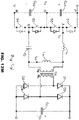
- FIGs. 1A and 1B show, respectively, an exemplary conventional full-bridge LLC resonant converter under closed-loop voltage control, and its timing diagrams for switch control signals and primary-side full-bridge output voltage V AB .
- Output voltage V o may be regulated by controlling the switching frequency of these primary-side switches.
- Highest efficiency is attained when the LLC resonant converter operates at the resonant frequency (f r ), which is determined by resonant inductor L r and resonant capacitor C r , and when the DC voltage gain M equals the transformer's turns ratio N P N S , wherein M equals V o /V in .
- DC voltage gain M diminishes when the switching frequency (f sw ) is greater than resonant frequency f r . Conversely, the gain M becomes greater when switching frequency f sw is less than resonant frequency f r . Efficiency, however, always diminishes as switching frequency f sw moves away from resonant frequency f r . To achieve a wide output voltage range, the LLC resonant converter operates at a very wide frequency range, which inevitably compromises its efficiency.
- the LLC resonant converter may be unable to achieve a very wide output voltage range under all load conditions.
- FIGS. 2A and 2B show, respectively, Mumtahina's full-bridge LLC resonant converter with closed-loop voltage control, and its timing diagrams under phase-shift control for switch control signals and primary-side full-bridge output voltage V AB .
- Mumtahina teaches providing a phase shift between the two pairs of gate signals at the two legs of the primary side switches. Using both phase-shift control and switching frequency control, Mumtahina's LLC resonant converter operates at a lower switching frequency in a voltage step-down operation.
- FIGs. 3A and 3B show, respectively, Jovanovic's full-bridge LLC resonant converter under topology-morphing control, and its timing diagrams for switch control signals during a full-bridge to half-bridge topology transition.
- Jovanovic the circuit topology adapts to the control signals, which in return respond to the input or output operating conditions.
- FIG. 4 is a circuit diagram for Jang's SRC.
- a variable frequency control scheme is applied to the primary-side switches, while a delay-time control scheme is applied to the secondary-side switches. The result is a boost to the output voltage, thus achieving a wider output voltage range, under control of a narrower switching frequency range.
- the input voltage to the LLC resonant converter must be high enough to avoid an undesirably high DC gain.
- each switching device on the primary side is required to block the full input voltage (see, e.g., the LLC resonant converter shown in FIG. 1A )
- a higher input voltage results in an increased cost in high voltage components.
- the input voltage to the LLC resonant converter must be high enough to avoid an undesirably high DC gain.
- a three-level topology in which each switching device blocks only one-half of the input voltage, is a more attractive alternative than the conventional full-bridge topology of FIG. 1A , and a three-level topology is disclosed, for example, in the article "The three-level ZVS PWM converter-a new concept in high voltage DC-to-DC conversion" (“Pinheiro"), by J. R. Pinheiro and I. Barbi, published in the Proceedings of the 1992 International Conference on Industrial Electronics, Control, Instrumentation, and Automation, San Diego, CA, USA, 1992, pp. 173-178 vol.1 .
- SHB serial half bridge
- a half-input voltage, two-level modulation scheme for a DC/DC converter is disclosed in the article " Asymmetrical Duty Cycle-Controlled LLC Resonant Converter With Equivalent Switching Frequency Doubler” (Zong”), by S. Zong, et al., published in IEEE Transactions on Power Electronics, vol. 31, no. 7, pp. 4963-4973, 7 2016 .
- Zong halves the switching frequency of the primary switches to reduce the driving loss.
- FIGs. 5A and 5B show, respectively, the circuit diagram and timing diagrams for the gate signals, demonstrating the two-level modulation schemes may also be effective approaches to regulate the output voltage.
- FIGS 6A and 6B show, respectively, the circuit diagram and timing diagrams for the gate signals in Liu's DC/DC converters.
- Liu's gate signals of each half-bridge are not complementary, which increases the complexity of the gate driving circuit.
- the body diode of the MOSFETs conducts current due to the non-optimized gate signals, which increases conduction loss and reduces system efficiency.
- a method of the embodiment of the present invention may use both modulation scheme control and device switching frequency control.
- the modulation scheme may be selected in response to one or more control signals provided from a controller or in an external command.
- the device switching frequency may be determined, for example, under a closed-loop control of a regulated output voltage.
- the controller may generate the control signals that drive the primary-side switching devices of the SHB LLC resonant converter.
- the SHB LLC resonant converter operates under a symmetrical modulation scheme, with its device switching frequency being adjusted under closed-loop control.
- the SHB LLC resonant converter operates under an asymmetrical modulation scheme, with device switching frequency control.
- the SHB LLC resonant converter operates under a narrower device switching frequency range with improved efficiency, while still achieving a very wide output-voltage range under different load conditions.
- the methods of the present invention have lesser restrictions on certain circuit parameters (e.g., the L m -to- L r ratio) while achieving desired minimum and maximum DC voltage gains.
- the methods of the present invention are applicable to resonant converters with different secondary-side topologies and secondary-side control schemes.
- the methods of the present invention operate under both fixed input-voltage and variable input-voltage conditions.
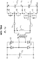
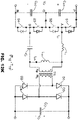
- FIG. 7A shows a 3-level SHB topology (also known as "stacked buck topology") that provides LLC resonant converter 700 that has a serial half-bridge on the primary-side.
- the serial half-bridge includes four series-connected switching devices S 1 to S 4 , configured such that each switching device S 1 to S 4 blocks one-half of the input voltage across input terminals P and N.
- the input terminals P and N are provided across series-connected input capacitors C in1 and C in2 , and across the switching devices S 1 and S 4 .
- the common terminal of the input capacitors C in1 and C in2 is also the common terminal between the switching devices S 2 and S 3 , such that the input capacitor C in1 is connected in parallel with the switching devices S 1 and S 2 , and the input capacitor C in2 is connected in parallel with the switching devices S 3 and S 4 .
- a full-wave diode rectifier D 1 to D 4 is provided on the secondary side.
- a filter capacitor C o is provided on the secondary side and configured to provide the output voltage V o or output current I o to the load.
- a first phase-leg output terminal A is provided at the common terminal between the switching devices S 1 and S 2
- a second phase-leg output terminal B is provided at the common terminal between the switching devices S 3 and S 4
- Connected across the terminals A and B is a resonant circuit formed by isolation transformer TR and series-connected resonant inductor L r , resonant capacitor C r , and transformer magnetizing inductor L m .
- the primary-side winding of the isolation transformer TR is connected in parallel with the magnetizing inductor L m .
- the secondary-side winding of the isolation transformer TR may be either (i) a center-tapped winding with two rectification components, or (ii) a single winding with a full-bridge rectifier.
- Each of the switching devices S 1 to S 4 blocks its share of the input voltage in one direction, but each conducts a current in both directions.
- Each of the switching devices S 1 to S 4 may be implemented by a semiconductor switch (e.g., MOSFET, IGBT, BJT or another semiconductor switch).
- the secondary-side may be implemented by a synchronous rectifier, which reduces conduction loss.
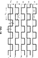
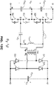
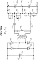
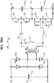
- FIGs. 7B and 7C illustrate, respectively, "symmetrical” and “asymmetrical” modulation schemes for the SHB LLC resonant converter 700 of FIG. 7A .
- Each modulation scheme controls the switch control signals to operate the switching devices S 1 to S 4 .
- the signals that operate the switching devices S 1 and S 2 are complementary, and the signals for operating the switching devices S 3 and S 4 are also complementary.
- a small dead-time is inserted between each pair of complementary switch control signals to avoid a phase-leg shoot-through.
- FIG. 7B shows, under symmetrical modulation, the timing diagrams of the switch control signals for the switching devices S 1 to S 4 and phase-leg output voltage V AB .
- the switch control signals operating the switching devices S 1 and S 4 are in-phase signals having the same 50% duty cycle waveform.
- the switch control signals operating the switching devices S 2 and S 3 are also in-phase signals having the same 50% duty cycle waveform, except that the switch control signals operating the switching devices S 1 and S 4 are complementary to the switch control signals operating the switching devices S 2 and S 3 . Consequently, the phase leg output voltage V AB (i.e., bridge output voltage) switches between V in and 0 with a 50% duty cycle at the device switching frequency.
- V AB i.e., bridge output voltage
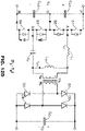
- FIG. 7C shows, under asymmetrical modulation, the timing diagrams of the switch control signals to the switching devices S 1 to S 4 and phase-leg output voltage V AB .
- the switch control signals that operate the switching devices S 1 and S 4 are 25% duty cycle signals that are phase-shifted 180° of each other, while the switch control signals that operate the switching devices S 2 and S 3 are 75% duty cycle signals that are also phase-shifted 180° of each other.
- the voltage across the input capacitor C in1 is provided as the phase-leg output voltage V AB when the switching devices S 1 and S 3 are closed
- the voltage across the input capacitor C in1 is provided as the phase-leg output voltage V AB when the switching devices S 2 and S 4 are closed
- the phase-leg output voltage V AB is zero volts when the switching devices S 2 and S 3 are closed.
- the phase-leg output voltage V AB switches between 0.5V in and 0 volts at 50% duty cycle at twice device switching frequency f sw .
- device switching frequency f sw may be a control variable that helps achieve different control targets.
- Symmetrical and asymmetrical modulation schemes of FIGs. 7B and 7C each generates a different phase-leg output voltage V AB across the series-connected L r -C r -L m resonant circuit; the phase-leg output voltage V AB includes different DC and AC components.
- the resonant capacitor C r blocks the DC component, so that only the AC component appears across the primary-side windings of the isolation transformer TR.
- the output voltage V O equals the average of the product of the rectified AC component of the phase leg output voltage V AB and a transformer voltage gain.
- the output voltage V O is given by: where V AB _ ac is the average of the rectified AC component of the phase-leg output voltage V AB .
- the AC component of the phase-leg output voltage V AB is a 50% duty cycle bipolar square-wave with amplitude at the device switching frequency f sw , such that the DC voltage gain at the resonant frequency f r is
- the AC component of the phase-leg output voltage V AB is a 50% duty cycle bipolar square-wave with amplitude at twice the device switching frequency f sw , such that the DC voltage gain at the resonant frequency f r is
- the DC voltage gain at the resonant frequency f r under symmetrical modulation is twice the DC voltage gain at the resonant frequency f r under asymmetrical modulation
- the voltage gain for the LLC resonant converter 700 may be adjusted by switching frequency control.
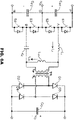
- FIG. 8 is a schematic diagram showing SHB LLC resonant converter 800, which includes a control circuit 801 that generates switch control signals to switching devices S 1 to S 4 based on output voltage V o (and, optionally, output current I o ), according to one embodiment of the present invention.
- the control circuit 801 may use the output voltage V O as its main control target.
- Output current I O may also be used as either a separate control target or as a feedback signal representative of a load condition.
- a reference value representative of each control target may be generated internally in the control circuit 801 or from an external source.
- the selected modulation scheme may be selected by the control circuit under direction of an external management controller. Based on a difference between the sensed voltage V o (or the sensed current I o ) and the corresponding reference value, the control circuit 801 switches among two or more modulation schemes that operate the switching devices S 1 to S 4 on the primary-side phase leg of SHB LLC resonant converter 800.
- One or more of the control targets may be used to determine values of other control parameters, such as device switching frequency f sw and a phase-shift in the selected modulation scheme.
- the switch control signals that operate the switching devices S 1 to S 4 on the primary side are generated based on the selected modulation scheme and other control parameter values.
- the transformer turns ratio Ns Np of the isolation transformer TR which is merely a scale factor in this instance, is set to 1, to simplify this detailed description.
- the symmetrical modulation scheme provides twice the output voltage Vo as the asymmetrical modulation scheme at the device switching frequency f sw at or about the resonant frequency f r .
- the phase-leg output voltage V AB (and, hence, output voltage V o also) at the resonant frequency f r is 0.5V in .
- the resonant parameters of the isolation transformer TR are such that, when the device switching frequency f sw varies from 0.5f r to 1.4f r , the output voltage V o varies from 0.3V in to 0.8V in .
- the phase-leg output voltage V AB (and, hence, output voltage V o also) at the resonant frequency f r is 0.25V in .
- the resonant parameters of the isolation transformer TR are such that, when the device switching frequency f sw varies from 0.25 f r to 0.8 f r , the output voltage V o varies from 0.125V in to 0.4V in .
- the present invention further provides a control method that combines a selection of a modulation scheme and frequency control to achieve a predetermined output voltage range.
- the modulation schemes may overlap in their respective output voltage regulation ranges.
- Modulation scheme selection under the embodiment of the present invention may be based, for example, on control parameters such as voltage control target, load condition, and allowable operating frequency range.
- the control circuit 801 effectuates a transition from the current modulation scheme to the preferred modulation scheme.
- SHB LLC resonant converter 800 may have an output voltage range V o between 0.125V in and 0.8V in , with the device switching frequency f sw ranged between 0.25 f r to 1.6 f r .
- the maximum-to-minimum DC gain ratio is 6.4, and the maximum device switching frequency f sw is only 1.6 f r .
- the device switching frequency f sw is not required to increase significantly, as in the case of conventional frequency control, thereby significantly switching loss.
- the device switching frequency f sw is even reduced when the frequency-doubling asymmetrical modulation scheme is used for the low output voltage.
- the maximum device switching frequency f sw is largely reduced under a method of the embodiment of the present invention especially at very low output voltage, at very light load condition or both.
- FIGs. 9A and 9B illustrate, respectively, switch control signals for the switching devices S 1 and S 4 and phase-leg output voltage V AB , as the control scheme switches (i) from a symmetrical modulation scheme to an asymmetrical modulation scheme, and (ii) from an asymmetrical modulation scheme to a symmetrical modulation scheme, according to one embodiment of the present invention.
- FIG. 9A illustrates a transition from a symmetrical modulation scheme (interval 901) to an asymmetrical modulation scheme (interval 903) when the output voltage control target changes from a high voltage to a low voltage in the output voltage range.
- Transition period 902 between the modulation schemes can be implemented in different ways, such as frequency shift, phase shift, duty cycle shift, or any of their combinations.
- FIG 9 B illustrates a transition from an asymmetrical modulation scheme (interval 904) to a symmetrical modulation scheme (interval 906) when the output voltage control target changes from a low voltage to a high voltage in the output voltage range.
- Transition period 905 between the modulation schemes can be implemented in the way as in the transition of FIG. 9A , i.e., using control parameters such as frequency shift, phase shift, duty cycle shift, or any of their combinations, but in reverse order. Of course, any other suitable transition control methods may also be used.
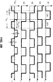
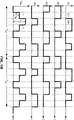
- FIG. 10B illustrates a three-level modulation scheme for the signals operating primary switching devices S 1 , S 2 , S 3 and S 4 of SHB LLC resonant converter 1000 of FIG. 10A .
- the signals that operate the switching devices S 1 and S 2 are complementary, and the signals for operating the switching devices S 3 and S 4 are also complementary.
- a small dead-time is inserted between each pair of complementary switch signals to avoid a phase-leg shoot-through.
- the control circuit is configurable to generate the first, second, third, and fourth switch control signals S 1 to S 4 according to a first modulation scheme in which (i) the first and the second switch control signals S 1 , S 2 are substantially complementary with each other and the third and the fourth switch control signals S 3 , S 4 are substantially complementary with each other, (ii) the first, second, third, and fourth switch control signals S 1 , S 2 , S 3 , S 4 are periodic with a common switching period T sw , (iii) within the common switching period T sw , (1) each switch control signal has two rising edges and two falling edges; and (2) the first rising edge of the first switch control signal S 1 lags the first rising edge of the fourth switch control signal S 4 by a first predetermined time, while the second rising edge of the first switch control signal S 1 leads the second rising edge for the fourth switch control signal S 4 by a second predetermined time, and (iv) the control circuit varies the switching period, the
- FIG. 10B shows the timing diagrams of the signals to primary switching devices S 1 to S 4 and SHB phase-leg output voltage V AB .
- switching period T sw each of primary switching devices S 1 , S 2 , S 3 and S 4 is turned on twice and turned off twice.
- primary switching device S 1 or S 4 has a fixed "on" duration that spans 25% of switching period T sw , such that the accumulated "on" duration is 50% of switching period T sw .
- FIG. 10B shows the timing diagrams of the signals to primary switching devices S 1 to S 4 and SHB phase-leg output voltage V AB .
- phase-leg output voltage V AB has three different voltage levels.
- phase-leg output voltage V AB equals 0.5V in .
- phase-leg output voltage V AB equals zero volts.
- the waveform of phase-leg output voltage V AB is periodical with a period that is half switching period T sw .
- duration ⁇ corresponds to the duration when primary switching devices S 2 and S 4 are both “on,” or when primary switching devices S 1 and S 3 are both “on,” duration ⁇ determines the duration over which phase-leg output voltage V AB equals 1 ⁇ 2 V in .
- Switching frequency f sw (hence, switching period T sw ) and duration ⁇ are the control variables for setting different control targets.
- ripple voltages of input capacitor C in and output capacitor C O are assumed negligible and thus may be represented by constant-voltage source V in and V O .
- the semiconductor circuit elements herein are each assumed to have zero resistance in its "on” or conducting state (i.e., they are considered short circuits).
- the output capacitances of the primary switching devices are not neglected.
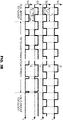
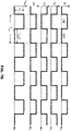
- FIG. 11 shows key waveforms of SHB LLC resonant converter 1000 of FIG. 10A during switching cycle T sw .
- FIG. 11 shows switch control voltages S 1 , S 2 , S 3 and S 4 (i.e., positive voltages indicate primary switching devices S 1 to S 4 , respectively, to be in the "on" state), primary-side output voltage V AB , current i Lr in resonant inductor L r , current i Lm in magnetizing inductor L m , and voltages V S1 and V S2 across primary switching devices S 1 and S 2 .
- FIG. 11 shows switch control voltages S 1 , S 2 , S 3 and S 4 (i.e., positive voltages indicate primary switching devices S 1 to S 4 , respectively, to be in the "on" state), primary-side output voltage V AB , current i Lr in resonant inductor L r , current i Lm in magnetizing inductor L m , and voltages V S
- 11 indicates signal transitions at times t 1 , t 2 , t 3 , t 4 , t 5 , t 6 , t 7 , t 8 , t 9 , t 10 , t 11 , t 12 , t 13 , t 14 , t 15 , and t 16 .
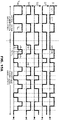
- FIGs. 12A-12P show sixteen operation stages of SHB LLC resonant converter 1000 under the 3-level modulation scheme of the embodiment of the present invention, corresponding to time periods (t 0 , t 1 ), (t 1 , t 2 ), (t 2 , t 3 ), (t 3 , t 4 ), (t 4 , t 5 ), (t 5 , t 6 ), (t 6 , t 7 ), (t 7 , tg), (tg, t 9 ), (t 9 , t 10 ), (t 10 , t 11 ), (t 11 , t 12 ), (t 12 , t 13 ), (t 13 , t 14 ), (t 14 , t 15 ), and (t 15 , t 16 ), respectively.
- an open or "off' switching device is indicated by dash-lines (e.g., in FIG. 12A , primary switching devices S 2 and S 3 are open). Also, parasitic capacitors of primary switching devices S 1 , S 2 , S 3 and S 4 are represented by capacitors C S1 , C S2 , C S3 and C S4 , respectively.
- Phase-leg output voltage V AB equals input voltage V in .
- capacitor C S1 charges to 1 ⁇ 2 V in and capacitor C S2 completely discharges (i.e., to zero volts across), after primary switching device S 1 becomes open.
- Current i Lr begins to decrease.
- Phase-leg output voltage V AB falls to 1 ⁇ 2 V in , as a result of the charging and discharging in capacitors C S1 and C S2 .
- phase-leg output voltage V AB remains at 1 ⁇ 2V in and current i Lr continues to decrease.
- capacitor C S4 charges to 1 ⁇ 2V in and capacitor C S3 discharges completely, after primary switching device S 4 is turned off.
- Phase-leg output voltage V AB goes to zero volts, as a result of the charging and discharging in capacitors C S4 and C S3 .
- Current i Lr continues to decrease.
- phase-leg output voltage V AB remains at zero volts and current i Lr continues to decrease.
- capacitor C S3 charges to 1 ⁇ 2 V in and capacitor C S4 discharges completely, after primary switching device S 3 is turned off.
- Phase-leg output voltage V AB rises to 1 ⁇ 2 V in and current i Lr begins to increase, as a result of the charging and discharging in capacitors C S3 and C S4 .
- phase-leg output voltage V AB remains at 1 ⁇ 2V in and current i Lr continues to increase.
- capacitor C S2 charges to 1 ⁇ 2 V in and capacitor C S1 discharges completely, after primary switching device S 2 is turned off.
- Phase-leg output voltage V AB becomes V in , as a result of the charging and discharging in capacitors C S2 and C S1 .
- Current i Lr continues to increase.
- phase-leg output voltage V AB remains at 1 ⁇ 2V in and current i Lr continues to increase.
- capacitor C S4 charges to 1 ⁇ 2 V in and capacitor C S3 completely discharges, after primary switching device S 4 becomes open.
- Current i Lr begins to decrease.
- Phase-leg output voltage V AB falls to 1 ⁇ 2 V in , as a result of the charging and discharging in capacitors C S4 and C S3 .
- phase-leg output voltage V AB remains at 1 ⁇ 2 V in and current i Lr continues to decrease.
- capacitor C S1 charges to 1 ⁇ 2V in and capacitor C S2 discharges completely, after primary switching device S 1 is turned off.
- Phase-leg output voltage V AB goes to zero volts, as a result of the charging and discharging in capacitors C S1 and C S2 .
- Current i Lr continues to decrease.
- phase-leg output voltage V AB remains at zero volts and current i Lr continues to decrease.
- capacitor C S2 charges to 1 ⁇ 2 V in and capacitor C S1 discharges completely, after primary switching device S 2 is turned off.
- Phase-leg output voltage V AB rises to 1 ⁇ 2 V in and current i Lr begins to increase, as a result of the charging and discharging in capacitors C S2 and C S1 .
- phase-leg output voltage V AB remains at 1 ⁇ 2V in and current i Lr continues to increase.
- capacitor C S3 charges to 1 ⁇ 2 V in and capacitor C S4 discharges completely, after primary switching device S 3 is turned off.
- Phase-leg output voltage V AB becomes V in , as a result of the charging and discharging in capacitors C S3 and C S4 .
- Current i Lr continues to increase.
- the 3-level modulation scheme of the embodiment of the present invention significantly reduce total switching loss.
- the three-level modulation scheme of the embodiment of the present invention generates, across the series-connected L r -C r -L m resonant circuit, controllable phase-leg output voltage V AB , which includes DC and AC components.
- resonant capacitor C r blocks the DC component, so that only the AC component appears across the primary-side windings of transformer TR.
- output voltage V O equals the average of the product of the rectified AC component of phase-leg output voltage V AB and transformer TR's voltage gain.
- output voltage V O is given by: where V AB_ac is the average of the rectified AC component of phase-leg output voltage V AB .
- V AB_ac is the average of the rectified AC component of phase-leg output voltage V AB .
- the average voltage of the rectified AC component reduces, if switching frequency f r is fixed. Accordingly, output voltage V O also decreases.
- the three-level modulation scheme of the embodiment of the present invention can be used to regulate output voltage V O without affecting switching frequency f r .
- the "on"-resistance of a power device gives rise to a conduction loss.
- primary switching devices S 1 to S 4 incur conduction loss when they are conducting.
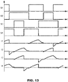
- FIG. 13 shows control switch voltages S 1 to S 4 in primary switching devices S 1 to S 4 , and the contemporaneous currents I 1 to I 4 flowing through them during switching period T sw , under the three-level modulation scheme of the embodiment of the present invention, without accounting for the effects of any dead-time.
- Currents I 1 to I 4 have the same root-mean-square (RMS) value, thereby balancing the thermal stress equally among the primary switching devices. Consequently, longer life in these devices may be expected, increasing the reliability of SHB LLC resonant converter 1000.
- RMS root-mean-square
- top and bottom capacitors e.g., capacitors C in1 and C in2
- their DC-link capacitor voltage is automatically balanced without any additional control.
- ESRs equivalent series resistances
- the capacitances of the DC-link capacitors and the timing mismatch of the switch control or gate signals are inevitable in any practical SHB LLC resonant converter.
- the embodiment of the present invention provides a method to balance the DC-link capacitor voltages and to keep the SHB LLC resonant converter operating in a safe range.
- capacitor C in1 has a greater voltage than capacitor C in2
- all transitions in the switch control signals to primary switching devices S 1 and S 2 are delayed by a short time period and all transitions in the switch control signals to primary switching devices S 3 and S 4 are brought forward by the same amount.
- capacitor C in2 has a greater voltage than capacitor C in1
- all transitions in the switch control signals to primary switching devices S 1 and S 2 are brought forward by a short time period and all transitions in the switch control signals to primary switching devices S 3 and S 4 are delayed by the same amount.
- the short time period adjustment preferably should not exceed 5% of the switching period T sw to avoid any adverse effect on the normal operations of the SHB LLC resonant converter.
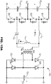
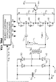
- FIG. 14 is a schematic diagram showing SHB LLC resonant converter 1400, which includes control circuit 1401 that generates switch control signals to primary switching devices S 1 to S 4 based on output voltage V O (and, optionally, output current I O ), according to one embodiment of the present invention.
- Control circuit 1401 in SHB LLC resonant converter 1400 may use output voltage V O as its main control target.
- Output current I O may also be used as either a separate control target or a feedback signal representative of a load condition.
- a reference value representative of each control target may be generated internally in control circuit 1401 or from an external source.
- control circuit 1401 switches among two or more modulation schemes that operate switching devices S 1 to S 4 on the primary-side phase leg of SHB LLC resonant controller 1401.
- One or more of the control targets may be used to determine values of other control parameters, such as switching frequency f sw and duty cycles of signals in the selected modulation scheme.
- the signals that operate primary-side switching devices S 1 to S 4 are generated based on the selected modulation scheme and other control parameter values.
- the conventional symmetrical frequency modulation scheme provides a desired output voltage gain by varying the switching frequency f sw about resonant frequency f r . While the proposed three-level modulation scheme provides extra output voltage gains at the maximum allowable switching frequency by controlling the durations the primary switching devices are conducting. Accordingly, the embodiment of the present invention provides a control method that combines a selected modulation scheme and frequency control to achieve a predetermined output voltage range. (The modulation schemes may overlap in their respective output voltage regulation ranges.) Modulation scheme selection of the embodiment under the present invention may be based, for example, on control parameters such as voltage control targets, load conditions, and an allowable operating frequency range.
- FIG. 15A illustrates, in SHB LLC resonant converter 1000, control signals for primary switching devices S 1 to S 4 and phase-leg output voltage V AB , as the control scheme switches from a symmetrical modulation scheme to a three-level modulation scheme.
- FIG. 15B illustrates, in SHB LLC resonant converter 1000, control signals for primary switching devices S 1 to S 4 and phase-leg output voltage V AB , as the control scheme switches from a three-level modulation scheme to a symmetrical modulation scheme, according to one embodiment of the present invention. As shown in FIG.
- switching from a symmetrical modulation scheme (interval 1501) to the three-level modulation scheme (interval 1592) of the embodiment of the present invention requires no transition period, as the control target for phase-leg output voltage V AB changes from a high voltage to a low voltage in output voltage V O .
- switching from the three-level modulation scheme of the embodiment of the present invention (interval 1503) to a symmetrical modulation scheme (interval 1504) also requires no transition period, as the control target for phase-leg output voltage V AB changes from a low voltage to a high voltage in output voltage V O .
- the symmetrical modulation scheme includes variable-frequency modulation.
- the symmetrical modulation scheme includes constant-frequency modulation.
- FIGs. 16A and 16B show, respectively, (i) SHB LLC resonant converter 1600 with a full-bridge synchronous rectifier on the secondary side, and (ii) SHB LLC resonant converter 1650 with center-tapped transformer TR and synchronous rectifiers S 5 and S 6 on the secondary side, according to one embodiment of the present invention.
- the control circuit 1601 may combine the methods discussed with respect to FIG.
- control circuit 1651 may combine the methods discussed with respect to FIG. 10B above with conventional secondary-side control schemes to generate the signals to operate the switching devices S 1 to S 4 on the primary-side and the switching devices S 5 to S 8 on the secondary-side.
- the control circuit 1651 may combine the methods discussed with respect to FIG. 10B above with conventional secondary-side control schemes to generate the signals to operate the switching devices S 1 to S 4 on the primary-side and the switching devices S 5 and S 6 on the secondary-side.
- the embodiment of the present invention is equally applicable to an SHB LLC resonant converter in which the switching devices S 5 to S 8 on the secondary-side of SHB LLC resonant converter 1600, or the switching devices S 5 to S 6 on the secondary-side of SHB LLC resonant converter 1650, are replaced by diodes.
- FIGs. 17A , and 17B show, respectively, (i) SHB LLC resonant converter 1700 with variable DC input voltage source 1702, and (i) SHB LLC resonant converter 1750 with DC input voltages V in1 and V in2 , respectively, controlled according to one embodiment of the present invention.
- variable DC input voltage source 1702 may be controlled by signal V ctrl , which may be internally generated or provided externally. Combining a control method for signal V ctrl with any of the methods of the embodiments of the present invention discussed above may further extend the output voltage range or further reduce the device switching frequency range of the SHB LLC resonant converter 1700.
Description
- This invention relates to power converters. More specifically, this invention relates to controlling a resonant DC/DC converter using various modulation schemes to attain regulation of an output voltage over a very wide voltage range.
- Many power conversion applications (e.g., battery charging in electrical vehicles (EVs)) require a regulated output voltage over a wide voltage range. For example, a typical EV battery charger circuit has two converter stages: (i) a front-end AC/DC converter that provides either a fixed DC bus voltage or a variable DC bus voltage, and (ii) an isolated DC/DC converter that directly interfaces with the battery. The DC/DC converter is required to provide a regulated voltage over a wide voltage range under various load current conditions and the battery's state of charge. For example, the typical battery for a conventional EV has a voltage range between 240 volts to 460 volts. However, some premium passenger EVs, utility EVs, and electrical buses or semi-trucks have output battery voltage range between 500 volts and 950 volts. Thus, a DC/DC converter that can provide a regulated output voltage over a very wide output voltage range is desired, so as to accommodate the charging requirements at different battery voltage levels.
- The LLC resonant converter topology has been widely used as an isolated DC/DC converter, due to its high efficiency, simple structure achieved by magnetic integration, soft switching on both primary and secondary switches, and capability suitable for applications with wide voltage ranges.
-
FIGs. 1A and1B show, respectively, an exemplary conventional full-bridge LLC resonant converter under closed-loop voltage control, and its timing diagrams for switch control signals and primary-side full-bridge output voltage VAB. Output voltage Vo may be regulated by controlling the switching frequency of these primary-side switches. Highest efficiency is attained when the LLC resonant converter operates at the resonant frequency (fr), which is determined by resonant inductor Lr and resonant capacitor Cr, and when the DC voltage gain M equals the transformer's turns ratio
- For wide output voltage range applications, such as battery charging applications, the LLC resonant circuit parameters must carefully trade-off between efficiency and the output voltage range. In the prior art, many techniques for achieving a wide output voltage range have been developed, such as those disclosed in:
- (a) "Design Methodology of LLC Resonant Converters for Electric Vehicle Battery Chargers," by J. Deng et al., published in the IEEE Transactions on Vehicular Technology, vol. 63, no. 4, pp. 1581-1592, May 2014;
- (b) "An LLC Resonant DC-DC Converter for Wide Output Voltage Range Battery Charging Applications," by F. Musavi et al., published in IEEE Transactions on Power Electronics, vol. 28, no. 12, pp. 5437-5445, Dec. 2013;
- (c) "A Design Procedure for Optimizing the LLC Resonant Converter as a Wide Output Range Voltage Source," by R. Beiranvand et al., published in the IEEE Transactions on Power Electronics, vol. 27, no. 8, pp. 3749-3763, Aug. 2012; and
- (d) "Optimal Design Methodology for LLC Resonant Converter in Battery Charging Applications Based on Time-Weighted Average Efficiency," by Z. Fang et al., published in the IEEE Transactions on Power Electronics, vol. 30, no. 10, pp. 5469-5483, Oct. 2015.
- (e) "Topology Evaluation and Comparison for Isolated Multilevel DC/DC Converter for Power Cell in Solid State Transformer", by Yang Jiao and Milan M. Jovanovic, published in the proceedings of the APPLIED POWER ELECTRONICS CONFERENCE AND EXPOSITION, APEC, pp. 802-809, March 2017.
- Nevertheless, these techniques can only optimize the converter circuits to achieve a limited output voltage range (e.g., between 200 volts and 500 volts) in conventional EV charging applications.
- To achieve a wider output voltage range with good efficiency, modifications of circuit structures and control schemes have been proposed for a conventional LLC resonant converter. For example, the article "Multimode Optimization of the Phase-Shifted LLC Series Resonant Converter" ("Mumtahina") by U. Mumtahina and P. J. Wolfs, published in IEEE Transactions on Power Electronics, vol. 33, no. 12, pp. 10478-10489, Dec. 2018, discloses an LLC resonant converter that combines conventional frequency control and phase-shift control schemes to achieve a wide output voltage range.
FIGs. 2A and2B show, respectively, Mumtahina's full-bridge LLC resonant converter with closed-loop voltage control, and its timing diagrams under phase-shift control for switch control signals and primary-side full-bridge output voltage VAB. Mumtahina teaches providing a phase shift between the two pairs of gate signals at the two legs of the primary side switches. Using both phase-shift control and switching frequency control, Mumtahina's LLC resonant converter operates at a lower switching frequency in a voltage step-down operation. -
U.S. Patent 9,263,960 B2 ("Jovanovic") to M. Jovanovic and B. Irving, entitled "Power Converters for Wide Input or Output Voltage Range and Control Methods Thereof," granted on Feb. 16, 2016 FIGs. 3A and3B show, respectively, Jovanovic's full-bridge LLC resonant converter under topology-morphing control, and its timing diagrams for switch control signals during a full-bridge to half-bridge topology transition. In Jovanovic, the circuit topology adapts to the control signals, which in return respond to the input or output operating conditions. -
U.S. Patent Application Publication 2015/0229225A1 ("Jang") by Y. Jang and M. Jovanovic, entitled "Resonant Converter and Control Methods Thereof," filed on August 13, 2015 , discloses a control scheme for a series resonant converter (SRC) that combines a variable-frequency control scheme with a delay-time control scheme.FIG. 4 is a circuit diagram for Jang's SRC. In Jang, a variable frequency control scheme is applied to the primary-side switches, while a delay-time control scheme is applied to the secondary-side switches. The result is a boost to the output voltage, thus achieving a wider output voltage range, under control of a narrower switching frequency range. - Many other variations in topologies and control schemes have been proposed for conventional LLC resonant converters to achieve wide output voltage ranges. However, these variations all have drawbacks, such as complexity in implementation, increased part count, or undesired dynamics. In addition, these variations still do not achieve a sufficiently wide output voltage range. For example, a 200-volt to 1000-volt EV fast-charger remains to be attained.
- One challenge in achieving a wide output voltage range is that the input voltage to the LLC resonant converter must be high enough to avoid an undesirably high DC gain. As each switching device on the primary side is required to block the full input voltage (see, e.g., the LLC resonant converter shown in
FIG. 1A ), a higher input voltage results in an increased cost in high voltage components. - To achieve a wide output voltage range, the input voltage to the LLC resonant converter must be high enough to avoid an undesirably high DC gain. In this regard, a three-level topology, in which each switching device blocks only one-half of the input voltage, is a more attractive alternative than the conventional full-bridge topology of
FIG. 1A , and a three-level topology is disclosed, for example, in the article "The three-level ZVS PWM converter-a new concept in high voltage DC-to-DC conversion" ("Pinheiro"), by J. R. Pinheiro and I. Barbi, published in the Proceedings of the 1992 International Conference on Industrial Electronics, Control, Instrumentation, and Automation, San Diego, CA, USA, 1992, pp. 173-178 vol.1. The three-level topology is described for LLC converters in the article "Three-level LLC series resonant DC/DC converter" ("Gu"), by Y. Gu, et al., published in IEEE Transactions on Power Electronics, vol. 20, no. 4, pp. 781-789, July 2005. Gu's LLC converters achieve zero-voltage switching (ZVS) for the switches without additional auxiliary circuit. - A three-level serial half bridge (SHB) topology, also known as stacked buck topology, is disclosed in the article "DC-DC converter: four switches Vpk =Vin/2, capacitive turn-off snubbing, ZV turn-on" ("Barbi"), by I. Barbi, et al. in IEEE Transactions on Power Electronics, vol. 19, no. 4, pp. 918-927, July 2004. Barbi removes the two clamping diodes in the conventional three-level topology of Pinheiro.
- A half-input voltage, two-level modulation scheme for a DC/DC converter is disclosed in the article "Asymmetrical Duty Cycle-Controlled LLC Resonant Converter With Equivalent Switching Frequency Doubler" (Zong"), by S. Zong, et al., published in IEEE Transactions on Power Electronics, vol. 31, no. 7, pp. 4963-4973, 7 2016. Zong halves the switching frequency of the primary switches to reduce the driving loss.
- For applications with wide input voltage ranges, both full input voltage, two-level modulation and half input voltage, two-level modulation schemes are applied to SHB LLC converters in the articles: (a) "Wide input voltage range compensation in DC/DC resonant architectures for on-board traction power supplies," by A. Coccia, et al., published in 2007 European Conference on Power Electronics and Applications, 2007; (b) "Variable Frequency Multiplier Technique for High-Efficiency Conversion Over a Wide Operating Range," by W. Inam, et al., publi Electronics, vol. 4, no. 2, pp. 335-343, June 2016; and (c) "Research on Dual-Operation Mode of 3-level LLC resonant converter," by A.Z. Li, et al., published in 2015 9th International Conference on Power Electronics and ECCE Asia (ICPE-ECCE Asia), 2015.
FIGs. 5A and5B show, respectively, the circuit diagram and timing diagrams for the gate signals, demonstrating the two-level modulation schemes may also be effective approaches to regulate the output voltage. - To achieve a wide output voltage range, the three-level modulation approach reduces the voltage gain once the maximum operating frequency has been reached. Under a three-level modulation scheme, however, the currents through the primary power switches are not balanced, which can cause thermal imbalance on the devices, shorten the device life and even lead to device damage. To balance the currents in the power switches, a periodically swapping modulation strategy is disclosed in the article "Periodically Swapping Modulation (PSM) Strategy for Three-Level (TL) DC/DC Converters With Balanced Switch Currents" ("Liu"), by D. Liu, et al., published in IEEE Transactions on Industrial Electronics, vol. 65, no. 1, pp. 412-423, January 2018.
FIGs. 6A and6B show, respectively, the circuit diagram and timing diagrams for the gate signals in Liu's DC/DC converters. However, Liu's gate signals of each half-bridge are not complementary, which increases the complexity of the gate driving circuit. In addition, the body diode of the MOSFETs conducts current due to the non-optimized gate signals, which increases conduction loss and reduces system efficiency. - Therefore, there is a need of providing an improved power converter in order to overcome the drawbacks of the conventional technologies.
- It is an object of the present invention to provide an isolated DC/DC converter for wide output voltage range and a control method thereof so as to address the above-mentioned issues encountered by the prior arts.
- This object is solved by the features of
device claim 1. The dependent claims recite advantageous embodiments of the invention. - Accordingly, highly efficient methods of the embodiments of the present invention enable an SHB LLC resonant converter to regulate an output voltage over a wide range using a narrow device switching frequency range. A method of the embodiment of the present invention may use both modulation scheme control and device switching frequency control. During operation, the modulation scheme may be selected in response to one or more control signals provided from a controller or in an external command. The device switching frequency may be determined, for example, under a closed-loop control of a regulated output voltage. Based on the selected modulation scheme and the device switching frequency, the controller may generate the control signals that drive the primary-side switching devices of the SHB LLC resonant converter.
- In one embodiment of the present invention, to achieve a regulated voltage in a high output-voltage range, the SHB LLC resonant converter operates under a symmetrical modulation scheme, with its device switching frequency being adjusted under closed-loop control. To achieve a regulated voltage in a low output-voltage range, the SHB LLC resonant converter operates under an asymmetrical modulation scheme, with device switching frequency control. Thus, the SHB LLC resonant converter operates under a narrower device switching frequency range with improved efficiency, while still achieving a very wide output-voltage range under different load conditions. In addition, the methods of the present invention have lesser restrictions on certain circuit parameters (e.g., the Lm -to- Lr ratio) while achieving desired minimum and maximum DC voltage gains. The methods of the present invention are applicable to resonant converters with different secondary-side topologies and secondary-side control schemes. The methods of the present invention operate under both fixed input-voltage and variable input-voltage conditions.
- The present invention is better understood upon consideration of the following detailed description and accompanying figures.
-
-
FIGs. 1A and1B show, respectively, an exemplary conventional full-bridge LLC resonant converter under closed-loop voltage control, and its timing diagrams for switch control signals and primary-side full-bridge output voltage VAB; -
FIGs. 2A and2B show, respectively, an exemplary conventional full-bridge LLC resonant converter with closed-loop voltage control, and its timing diagrams under phase-shift control for switch control signals and primary-side full-bridge output voltage VAB; -
FIGs. 3A and3B show, respectively, an exemplary conventional full-bridge LLC resonant converter under topology-morphing control, and its timing diagrams for switch control signals during a full-bridge to half-bridge topology transition; -
FIG. 4 shows an exemplary conventional full-bridge series-resonant converter under frequency and delay-time control; -
FIGs. 5A and5B show, respectively, an exemplary serial half-bridge LLC resonant converter and its timing diagrams under asymmetric three-level control for switch control signals S1 to S4 and primary-side output voltage VAB; -
FIGs. 6A and6B FIG. show, respectively, an exemplary serial half-bridge LLC resonant converter and its timing diagrams under periodically swapping three-level control for switch control signals S1 to S4 and primary-side output voltage VAB; -
FIGs. 7A ,7B and7C show, respectively, (i) exemplary serial half-bridge (SHB) LLCresonant converter 700 with a full-wave secondary-side diode rectifier, (ii) its timing diagrams under symmetrical modulation for switch control signals to switching devices S1 to S4 and phase leg output voltage VAB, and (iii) its timing diagrams under asymmetrical modulation for switch control signals to switching devices S1 to S4 and phase leg output voltage VAB; -
FIG. 8 is a schematic diagram showing SHB LLCresonant converter 800, which includescontrol circuit 801 that generates switch control signals for switching devices S1 to S4 based on output voltage Vo (and, optionally, output current Io ), according to one embodiment of the present invention; -
FIGs. 9A and9B illustrate, respectively, switch control signals for switching devices S1 to S4 and phase-leg output voltage VAB, as the control scheme switches (i) from a symmetrical modulation scheme to an asymmetrical modulation scheme, and (ii) from an asymmetrical modulation scheme to a symmetrical modulation scheme, according to one embodiment of the present invention; -
FIGs. 10A and10B show, respectively, serial half-bridge LLCresonant converter 1000 and its timing diagrams of (i) the control signals for primary switching devices S1 to S4, under a three-level modulation scheme, and (ii) primary-side output voltage VAB, according to one embodiment of the invention; -
FIG. 11 shows key waveforms of SHB LLCresonant converter 1000 ofFIG. 10A during switching cycle Tsw;FIG. 11 indicates signal transitions at times t1, t2, t3, t4, t5, t6, t7, t8, t9, t10, t11, t12, t13, t14, t15, and t16; -
FIGs. 12A-12P show sixteen operation stages of SHB LLCresonant converter 1000 under the 3-level modulation scheme of the embodiment of the present invention, corresponding to time periods (t0, t1), (t1, t2), (t2, t3), (t3, t4), (t4, t5), (t5, t6), (t6, t7), (t7, t8), (t8, t9), (t9, t10), (t10, t11), (t11, t12), (t12, t13), (t13, t14), (t14, t15), and (t15, t16), respectively; -
FIG. 13 shows control switch voltages S1 to S4 in primary switching devices S1 to S4, and the contemporaneous currents I1 to I4 flowing through them during switching period TSW, under the three-level modulation scheme of the embodiment of the present invention, without accounting for the effects of any dead-time; -
FIG. 14 is a schematic diagram showing SHB LLCresonant converter 1400, which includescontrol circuit 1401 that generates switch control signals to primary switching devices S1 to S4 based on output voltage VO (and, optionally, output current IO), according to one embodiment of the present invention; -
FIG. 15A illustrates control signals for primary switching devices S1 to S4 and phase-leg output voltage VAB, as the control scheme switches from a symmetrical modulation scheme to a three-level modulation scheme; -
FIG. 15B illustrates control signals for primary switching devices S1 to S4 and phase-leg output voltage VAB, as the control scheme switches from a three-level modulation scheme to a symmetrical modulation scheme, according to one embodiment of the present invention; -
FIGs. 16A and16B show, respectively, (i) SHB LLCresonant converter 1600 with a full-bridge synchronous rectifier on the secondary side, and (ii) SHB LLCresonant converter 1650 with center-tapped transformer TR and synchronous rectifiers S5 and S6 on the secondary side, according to one embodiment of the present invention; and -
FIGs. 17A , and17B show, respectively, (i) SHB LLCresonant converter 1700 with variable DCinput voltage source 1702, and (i) SHB LLCresonant converter 1750 with DC input voltages Vin1 and Vin2, respectively, controlled according to one embodiment of the present invention. - In summary, the subject-matter of
claim 1 is reflected byfigures 10B ,15A and15B . The other figures serve to explain various details of the converter topology, the transitions between the symmetrical and asymmetrical modulation schemes and the selection of the duty cycles, as defined by the dependent claims 2-14. - The present disclosure will now be described more specifically with reference to the following embodiments. It is to be noted that the following descriptions of preferred embodiments of this disclosure are presented herein for purpose of illustration and description only. It is not intended to be exhaustive or to be limited to the precise form disclosed.
- To avoid the higher cost associated with a higher input voltage, a multi-level topology may be used to maintain the same device voltage rating for the primary-side bridge.
FIG. 7A shows a 3-level SHB topology (also known as "stacked buck topology") that provides LLCresonant converter 700 that has a serial half-bridge on the primary-side. As shown inFIG. 7A , the serial half-bridge includes four series-connected switching devices S1 to S4, configured such that each switching device S1 to S4 blocks one-half of the input voltage across input terminals P and N. The input terminals P and N are provided across series-connected input capacitors Cin1 and Cin2, and across the switching devices S1 and S4. The common terminal of the input capacitors Cin1 and Cin2 is also the common terminal between the switching devices S2 and S3, such that the input capacitor Cin1 is connected in parallel with the switching devices S1 and S2, and the input capacitor Cin2 is connected in parallel with the switching devices S3 and S4. A full-wave diode rectifier D1 to D4 is provided on the secondary side. A filter capacitor Co is provided on the secondary side and configured to provide the output voltage Vo or output current Io to the load. - A first phase-leg output terminal A is provided at the common terminal between the switching devices S1 and S2, while a second phase-leg output terminal B is provided at the common terminal between the switching devices S3 and S4. Connected across the terminals A and B is a resonant circuit formed by isolation transformer TR and series-connected resonant inductor Lr, resonant capacitor Cr, and transformer magnetizing inductor Lm. The primary-side winding of the isolation transformer TR is connected in parallel with the magnetizing inductor Lm. The secondary-side winding of the isolation transformer TR may be either (i) a center-tapped winding with two rectification components, or (ii) a single winding with a full-bridge rectifier. Each of the switching devices S1 to S4 blocks its share of the input voltage in one direction, but each conducts a current in both directions. Each of the switching devices S1 to S4 may be implemented by a semiconductor switch (e.g., MOSFET, IGBT, BJT or another semiconductor switch). Alternately, instead of a diode rectifier circuit, the secondary-side may be implemented by a synchronous rectifier, which reduces conduction loss.
-
FIGs. 7B and7C illustrate, respectively, "symmetrical" and "asymmetrical" modulation schemes for the SHB LLCresonant converter 700 ofFIG. 7A . Each modulation scheme controls the switch control signals to operate the switching devices S1 to S4. In either modulation scheme, the signals that operate the switching devices S1 and S2 are complementary, and the signals for operating the switching devices S3 and S4 are also complementary. In practice, a small dead-time is inserted between each pair of complementary switch control signals to avoid a phase-leg shoot-through.FIG. 7B shows, under symmetrical modulation, the timing diagrams of the switch control signals for the switching devices S1 to S4 and phase-leg output voltage VAB. The switch control signals operating the switching devices S1 and S4 are in-phase signals having the same 50% duty cycle waveform. Likewise, the switch control signals operating the switching devices S2 and S3 are also in-phase signals having the same 50% duty cycle waveform, except that the switch control signals operating the switching devices S1 and S4 are complementary to the switch control signals operating the switching devices S2 and S3. Consequently, the phase leg output voltage VAB (i.e., bridge output voltage) switches between Vin and 0 with a 50% duty cycle at the device switching frequency. -
FIG. 7C shows, under asymmetrical modulation, the timing diagrams of the switch control signals to the switching devices S1 to S4 and phase-leg output voltage VAB. As shown inFIG. 7C , the switch control signals that operate the switching devices S1 and S4 are 25% duty cycle signals that are phase-shifted 180° of each other, while the switch control signals that operate the switching devices S2 and S3 are 75% duty cycle signals that are also phase-shifted 180° of each other. With this asymmetrical modulation, the voltage across the input capacitor Cin1 is provided as the phase-leg output voltage VAB when the switching devices S1 and S3 are closed, the voltage across the input capacitor Cin1 is provided as the phase-leg output voltage VAB when the switching devices S2 and S4 are closed, and the phase-leg output voltage VAB is zero volts when the switching devices S2 and S3 are closed. Thus, the phase-leg output voltage VAB switches between 0.5Vin and 0 volts at 50% duty cycle at twice device switching frequency fsw . In either modulation scheme, device switching frequency fsw may be a control variable that helps achieve different control targets. - Symmetrical and asymmetrical modulation schemes of
FIGs. 7B and7C each generates a different phase-leg output voltage VAB across the series-connected Lr-Cr-Lm resonant circuit; the phase-leg output voltage VAB includes different DC and AC components. During the LLCresonant converter 700 operations, the resonant capacitor Cr blocks the DC component, so that only the AC component appears across the primary-side windings of the isolation transformer TR. When device switching frequency fsw equals the resonant frequency


V AB_ac is the average of the rectified AC component of the phase-leg output voltage VAB. - For the symmetrical modulation, the AC component of the phase-leg output voltage VAB is a 50% duty cycle bipolar square-wave with amplitude


resonant converter 700 may be adjusted by switching frequency control. - As mentioned above, maximum efficiency is achieved when the LLC
resonant converter 700 is operated at the operating point at or very close to the resonant frequency fr . To achieve a wide output voltage range, conventional control changes the device switching frequency fsw to adjust the DC voltage gain. However, switching frequency control moves the operating point away from maximum circuit efficiency. Further, for a very wide output voltage range, even such a control may still be unable to achieve the required DC voltage gain because the fixed circuit parameters. - The inventors of the present invention recognize that a SHB LLC resonant converter can provide a very wide output voltage range, while efficiently achieving desirable different DC voltage gains at or near the resonant frequency (i.e., a narrower input switching frequency range), using a combination of different modulation schemes. Moreover, the control method of the embodiment of the present invention achieves the wide output voltage range and the circuit gains even though the circuit parameter values are fixed.
FIG. 8 is a schematic diagram showing SHB LLCresonant converter 800, which includes acontrol circuit 801 that generates switch control signals to switching devices S1 to S4 based on output voltage Vo (and, optionally, output current Io ), according to one embodiment of the present invention. - In SHB LLC
resonant converter 800, thecontrol circuit 801 may use the output voltage VO as its main control target. Output current IO may also be used as either a separate control target or as a feedback signal representative of a load condition. A reference value representative of each control target may be generated internally in thecontrol circuit 801 or from an external source. In an embodiment, the selected modulation scheme may be selected by the control circuit under direction of an external management controller. Based on a difference between the sensed voltage Vo (or the sensed current Io ) and the corresponding reference value, thecontrol circuit 801 switches among two or more modulation schemes that operate the switching devices S1 to S4 on the primary-side phase leg of SHB LLCresonant converter 800. One or more of the control targets may be used to determine values of other control parameters, such as device switching frequency fsw and a phase-shift in the selected modulation scheme. The switch control signals that operate the switching devices S1 to S4 on the primary side are generated based on the selected modulation scheme and other control parameter values. - In
FIGs. 9A and9B , the transformer turns ratio
FIGs. 7B and7C , the symmetrical modulation scheme provides twice the output voltage Vo as the asymmetrical modulation scheme at the device switching frequency fsw at or about the resonant frequency fr . Specifically, under symmetrical modulation, the phase-leg output voltage VAB (and, hence, output voltage Vo also) at the resonant frequency fr is 0.5Vin. In one embodiment, the resonant parameters of the isolation transformer TR are such that, when the device switching frequency fsw varies from 0.5fr to 1.4fr, the output voltage Vo varies from 0.3Vin to 0.8Vin. Likewise, under asymmetrical modulation, the phase-leg output voltage VAB (and, hence, output voltage Vo also) at the resonant frequency fr is 0.25Vin. In the same embodiment, the resonant parameters of the isolation transformer TR are such that, when the device switching frequency fsw varies from 0.25fr to 0.8fr , the output voltage Vo varies from 0.125Vin to 0.4Vin. (Recall that the device switching frequency fsw is only half the frequency of the phase-leg output voltage VAB.) Accordingly, the present invention further provides a control method that combines a selection of a modulation scheme and frequency control to achieve a predetermined output voltage range. (The modulation schemes may overlap in their respective output voltage regulation ranges.) Modulation scheme selection under the embodiment of the present invention may be based, for example, on control parameters such as voltage control target, load condition, and allowable operating frequency range. When one or more of the conditions change such that a modulation scheme different from the current scheme is preferred, thecontrol circuit 801 effectuates a transition from the current modulation scheme to the preferred modulation scheme. - In the embodiment described above, SHB LLC
resonant converter 800 may have an output voltage range Vo between 0.125Vin and 0.8Vin, with the device switching frequency fsw ranged between 0.25fr to 1.6fr . The maximum-to-minimum DC gain ratio is 6.4, and the maximum device switching frequency fsw is only 1.6fr . For a low output voltage, the device switching frequency fsw is not required to increase significantly, as in the case of conventional frequency control, thereby significantly switching loss. (In fact, the device switching frequency fsw is even reduced when the frequency-doubling asymmetrical modulation scheme is used for the low output voltage.) The maximum device switching frequency fsw is largely reduced under a method of the embodiment of the present invention especially at very low output voltage, at very light load condition or both. By adjusting circuit parameter values, an even higher maximum-to-minimum DC gain ratio can be achieved, over the same narrow device switching frequency range, which is not achieved in SHB LLC resonant converters using conventional control. -
FIGs. 9A and9B illustrate, respectively, switch control signals for the switching devices S1 and S4 and phase-leg output voltage VAB, as the control scheme switches (i) from a symmetrical modulation scheme to an asymmetrical modulation scheme, and (ii) from an asymmetrical modulation scheme to a symmetrical modulation scheme, according to one embodiment of the present invention.FIG. 9A illustrates a transition from a symmetrical modulation scheme (interval 901) to an asymmetrical modulation scheme (interval 903) when the output voltage control target changes from a high voltage to a low voltage in the output voltage range.Transition period 902 between the modulation schemes can be implemented in different ways, such as frequency shift, phase shift, duty cycle shift, or any of their combinations. Likewise,FIG 9 B illustrates a transition from an asymmetrical modulation scheme (interval 904) to a symmetrical modulation scheme (interval 906) when the output voltage control target changes from a low voltage to a high voltage in the output voltage range.Transition period 905 between the modulation schemes can be implemented in the way as in the transition ofFIG. 9A , i.e., using control parameters such as frequency shift, phase shift, duty cycle shift, or any of their combinations, but in reverse order. Of course, any other suitable transition control methods may also be used. - According to one embodiment of the present invention,
FIG. 10B illustrates a three-level modulation scheme for the signals operating primary switching devices S1, S2, S3 and S4 of SHB LLCresonant converter 1000 ofFIG. 10A . The signals that operate the switching devices S1 and S2 are complementary, and the signals for operating the switching devices S3 and S4 are also complementary. In practice, a small dead-time is inserted between each pair of complementary switch signals to avoid a phase-leg shoot-through. In this embodiment, based on the output voltage or the output current, the control circuit is configurable to generate the first, second, third, and fourth switch control signals S1 to S4 according to a first modulation scheme in which (i) the first and the second switch control signals S1, S2 are substantially complementary with each other and the third and the fourth switch control signals S3, S4 are substantially complementary with each other, (ii) the first, second, third, and fourth switch control signals S1, S2, S3, S4 are periodic with a common switching period Tsw, (iii) within the common switching period Tsw, (1) each switch control signal has two rising edges and two falling edges; and (2) the first rising edge of the first switch control signal S1 lags the first rising edge of the fourth switch control signal S4 by a first predetermined time, while the second rising edge of the first switch control signal S1 leads the second rising edge for the fourth switch control signal S4 by a second predetermined time, and (iv) the control circuit varies the switching period, the first predetermined time, and the second predetermined time. In an embodiment, the control circuit varies the switching period about substantially one cycle of a resonant frequency of the LC resonant circuit. -
FIG. 10B shows the timing diagrams of the signals to primary switching devices S1 to S4 and SHB phase-leg output voltage VAB. In switching period Tsw, each of primary switching devices S1, S2, S3 and S4 is turned on twice and turned off twice. Each time it is turned on, primary switching device S1 or S4 has a fixed "on" duration that spans 25% of switching period Tsw, such that the accumulated "on" duration is 50% of switching period Tsw. As shown inFIG. 10B , during switching period Tsw, the first rising edge for primary switching device S1 lags the first of rising edge for primary switching device S4, while the second rising edge for primary switching device S1 leads the second rising edge for primary switching device S4. The lead and lag times are each ϕ, as shown inFIG. 10B . In addition, the first rising edge for primary switching device S1 leads the second rising edge for primary switching device S4 by ½ Tsw. Operating primary switching devices S1, S2, S3, and S4 in this manner, phase-leg output voltage VAB has three different voltage levels. In this embodiment, (i) when the first and fourth switching devices S1, S4 are both non-conducting, the voltage across the first and second electrical nodes goes to a first voltage level, (ii) when one of the first and fourth switching devices S1, S4 is conducting, the voltage across the first and second electrical nodes goes to a second voltage level, and (iii) when the first and fourth switching devices S1, S4 are both conducting, the voltage across the first electrical node goes to a third voltage level. The first voltage level may be ground, the second voltage level may be substantially one-half the input signal, and the second voltage level may be substantially the input signal. When primary switching devices S1 and S4 are both "on" or conducting, phase-leg output voltage VAB equals Vin. When primary switching devices S2 and S4 are both "on," or when primary switching devices S1 and S3 are both "on," phase-leg output voltage VAB equals 0.5Vin. When primary switching devices S2 and S3 are both "on", phase-leg output voltage VAB equals zero volts. - Thus, the waveform of phase-leg output voltage VAB is periodical with a period that is half switching period Tsw. As duration ϕ corresponds to the duration when primary switching devices S2 and S4 are both "on," or when primary switching devices S1 and S3 are both "on," duration ϕ determines the duration over which phase-leg output voltage VAB equals ½ Vin. Switching frequency fsw (hence, switching period Tsw) and duration ϕ are the control variables for setting different control targets.
- In this detailed description, to simplify the analysis of the operations, ripple voltages of input capacitor Cin and output capacitor CO, as shown in
FIG. 10A , are assumed negligible and thus may be represented by constant-voltage source Vin and VO. Also, the semiconductor circuit elements herein are each assumed to have zero resistance in its "on" or conducting state (i.e., they are considered short circuits). However, the output capacitances of the primary switching devices are not neglected. -
FIG. 11 shows key waveforms of SHB LLCresonant converter 1000 ofFIG. 10A during switching cycle Tsw.FIG. 11 shows switch control voltages S1, S2, S3 and S4 (i.e., positive voltages indicate primary switching devices S1 to S4, respectively, to be in the "on" state), primary-side output voltage VAB, current iLr in resonant inductor Lr, current iLm in magnetizing inductor Lm, and voltages VS1 and VS2 across primary switching devices S1 and S2.FIG. 11 indicates signal transitions at times t1, t2, t3, t4, t5, t6, t7, t8, t9, t10, t11, t12, t13, t14, t15, and t16. - In conjunction with
FIG. 11 ,FIGs. 12A-12P show sixteen operation stages of SHB LLCresonant converter 1000 under the 3-level modulation scheme of the embodiment of the present invention, corresponding to time periods (t0, t1), (t1, t2), (t2, t3), (t3, t4), (t4, t5), (t5, t6), (t6, t7), (t7, tg), (tg, t9), (t9, t10), (t10, t11), (t11, t12), (t12, t13), (t13, t14), (t14, t15), and (t15, t16), respectively. InFIGs. 12A-12P , an open or "off' switching device is indicated by dash-lines (e.g., inFIG. 12A , primary switching devices S2 and S3 are open). Also, parasitic capacitors of primary switching devices S1, S2, S3 and S4 are represented by capacitors CS1, CS2, CS3 and CS4, respectively. - During time period (t0, t1), as shown in
FIG. 12A , resonant current iLr increases and flows in resonant inductor Lr, transformer TR, magnetizing inductor Lm, resonant capacitor Cr, and primary switching devices S1 and S4. Phase-leg output voltage VAB equals input voltage Vin. - During time period (t1, t2), as shown in
FIG. 12B , capacitor CS1 charges to ½ Vin and capacitor CS2 completely discharges (i.e., to zero volts across), after primary switching device S1 becomes open. Current iLr begins to decrease. Phase-leg output voltage VAB falls to ½ Vin, as a result of the charging and discharging in capacitors CS1 and CS2. - During time period (t2, t3), as shown in
FIG. 12C , primary switching device S2 turns on at zero volts (i.e., at "ZVS" condition, with no switching loss). Phase-leg output voltage VAB remains at ½Vin and current iLr continues to decrease. - During time period (t3, t4), as shown in
FIG. 12D , capacitor CS4 charges to ½Vin and capacitor CS3 discharges completely, after primary switching device S4 is turned off. Phase-leg output voltage VAB goes to zero volts, as a result of the charging and discharging in capacitors CS4 and CS3. Current iLr continues to decrease. - During time period (t4, t5), as shown in
FIG. 12E , primary switching device S3 turns on at ZVS condition. Phase-leg output voltage VAB remains at zero volts and current iLr continues to decrease. - During time period (t5, t6), as shown in
FIG. 12F , capacitor CS3 charges to ½ Vin and capacitor CS4 discharges completely, after primary switching device S3 is turned off. Phase-leg output voltage VAB rises to ½ Vin and current iLr begins to increase, as a result of the charging and discharging in capacitors CS3 and CS4. - During time period (t6, t7), as shown in
FIG. 12G , primary switching device S4 turns on at ZVS condition. Phase-leg output voltage VAB remains at ½Vin and current iLr continues to increase. - During time period (t7, t8), as shown in
FIG. 12H , capacitor CS2 charges to ½ Vin and capacitor CS1 discharges completely, after primary switching device S2 is turned off. Phase-leg output voltage VAB becomes Vin, as a result of the charging and discharging in capacitors CS2 and CS1. Current iLr continues to increase. - During time period (t8, t9), as shown in
FIG. 121 , primary switching device S1 turns on at ZVS condition. Phase-leg output voltage VAB remains at ½Vin and current iLr continues to increase. - During time period (t9, t10), as shown in
FIG. 12J , capacitor CS4 charges to ½ Vin and capacitor CS3 completely discharges, after primary switching device S4 becomes open. Current iLr begins to decrease. Phase-leg output voltage VAB falls to ½ Vin, as a result of the charging and discharging in capacitors CS4 and CS3. - During time period (t10, t11), as shown in
FIG. 12K , primary switching device S3 turns on at ZVS condition. Phase-leg output voltage VAB remains at ½ Vin and current iLr continues to decrease. - During time period (t11, t12), as shown in
FIG. 12L , capacitor CS1 charges to ½Vin and capacitor CS2 discharges completely, after primary switching device S1 is turned off. Phase-leg output voltage VAB goes to zero volts, as a result of the charging and discharging in capacitors CS1 and CS2. Current iLr continues to decrease. - During time period (t12, t13), as shown in
FIG. 12M , primary switching device S2 turns on at ZVS condition. Phase-leg output voltage VAB remains at zero volts and current iLr continues to decrease. - During time period (t13, t14), as shown in
FIG. 12N , capacitor CS2 charges to ½ Vin and capacitor CS1 discharges completely, after primary switching device S2 is turned off. Phase-leg output voltage VAB rises to ½ Vin and current iLr begins to increase, as a result of the charging and discharging in capacitors CS2 and CS1. - During time period (t14, t15), as shown in
FIG. 120 , primary switching device S1 turns on at ZVS condition. Phase-leg output voltage VAB remains at ½Vin and current iLr continues to increase. - During time period (t15, t16), as shown in
FIG. 12P , capacitor CS3 charges to ½ Vin and capacitor CS4 discharges completely, after primary switching device S3 is turned off. Phase-leg output voltage VAB becomes Vin, as a result of the charging and discharging in capacitors CS3 and CS4. Current iLr continues to increase. - As all the primary switching devices turn on at ZVS conditions, the 3-level modulation scheme of the embodiment of the present invention significantly reduce total switching loss.
- Advantages of the three-level modulation scheme of the present invention: A. Reducing output voltage
- The three-level modulation scheme of the embodiment of the present invention generates, across the series-connected Lr-Cr-Lm resonant circuit, controllable phase-leg output voltage VAB, which includes DC and AC components. In this embodiment, during LLC resonant converter operations, resonant capacitor Cr blocks the DC component, so that only the AC component appears across the primary-side windings of transformer TR. When device switching frequency fsw equals resonant frequency


VAB_ac is the average of the rectified AC component of phase-leg output voltage VAB. For a desired value of duration ϕ, the average voltage of the rectified AC component reduces, if switching frequency fr is fixed. Accordingly, output voltage VO also decreases. Thus, the three-level modulation scheme of the embodiment of the present invention can be used to regulate output voltage VO without affecting switching frequency fr . - The "on"-resistance of a power device gives rise to a conduction loss. In SHB LLC
resonant converter 1000 ofFIG. 10A , primary switching devices S1 to S4 incur conduction loss when they are conducting.FIG. 13 shows control switch voltages S1 to S4 in primary switching devices S1 to S4, and the contemporaneous currents I1 to I4 flowing through them during switching period Tsw , under the three-level modulation scheme of the embodiment of the present invention, without accounting for the effects of any dead-time. Currents I1 to I4 have the same root-mean-square (RMS) value, thereby balancing the thermal stress equally among the primary switching devices. Consequently, longer life in these devices may be expected, increasing the reliability of SHB LLCresonant converter 1000. - Ideally, when the top and bottom capacitors (e.g., capacitors Cin1 and Cin2) deliver the same power to the resonant tank under the three-level modulation scheme of the embodiment of the present invention, their DC-link capacitor voltage is automatically balanced without any additional control. However, both the parameter mismatch of the equivalent series resistances (ESRs) and the capacitances of the DC-link capacitors and the timing mismatch of the switch control or gate signals are inevitable in any practical SHB LLC resonant converter. These mismatches result in DC-link capacitor voltage imbalances.
- The embodiment of the present invention provides a method to balance the DC-link capacitor voltages and to keep the SHB LLC resonant converter operating in a safe range. When capacitor Cin1 has a greater voltage than capacitor Cin2, all transitions in the switch control signals to primary switching devices S1 and S2 are delayed by a short time period and all transitions in the switch control signals to primary switching devices S3 and S4 are brought forward by the same amount. Similarly, when capacitor Cin2 has a greater voltage than capacitor Cin1, all transitions in the switch control signals to primary switching devices S1 and S2 are brought forward by a short time period and all transitions in the switch control signals to primary switching devices S3 and S4 are delayed by the same amount. The short time period adjustment preferably should not exceed 5% of the switching period Tsw to avoid any adverse effect on the normal operations of the SHB LLC resonant converter.
- As mentioned above, maximum efficiency is achieved when the SHB LLC resonant converter is operated at an operating point at or very close to resonant frequency fr . To achieve a wide output voltage range, conventional control modulates switching frequency fsw to adjust the DC voltage gain. However, switching frequency control moves the operating point away from maximum circuit efficiency. Further, for a very wide output voltage range, even such switching frequency control is unable to achieve the required DC voltage gain due to the fixed circuit parameters.
- The inventors of the present invention recognize that an SHB LLC resonant converter can provide a wide output voltage range, while efficiently achieving desirable different DC voltage gains at or near the resonant frequency (i.e., a narrower input switching frequency range), using a combination of different modulation schemes. Moreover, the three-level modulation scheme of the embodiment of the present invention achieves the wide output voltage range and the circuit gains even when the circuit parameter values are fixed.
FIG. 14 is a schematic diagram showing SHB LLCresonant converter 1400, which includescontrol circuit 1401 that generates switch control signals to primary switching devices S1 to S4 based on output voltage VO (and, optionally, output current IO), according to one embodiment of the present invention. -
Control circuit 1401 in SHB LLCresonant converter 1400 may use output voltage VO as its main control target. Output current IO may also be used as either a separate control target or a feedback signal representative of a load condition. A reference value representative of each control target may be generated internally incontrol circuit 1401 or from an external source. Based on a difference between the sensed voltage VO (or the sensed current IO) and the corresponding reference value,control circuit 1401 switches among two or more modulation schemes that operate switching devices S1 to S4 on the primary-side phase leg of SHB LLCresonant controller 1401. One or more of the control targets may be used to determine values of other control parameters, such as switching frequency fsw and duty cycles of signals in the selected modulation scheme. The signals that operate primary-side switching devices S1 to S4 are generated based on the selected modulation scheme and other control parameter values. - The conventional symmetrical frequency modulation scheme provides a desired output voltage gain by varying the switching frequency fsw about resonant frequency fr. While the proposed three-level modulation scheme provides extra output voltage gains at the maximum allowable switching frequency by controlling the durations the primary switching devices are conducting. Accordingly, the embodiment of the present invention provides a control method that combines a selected modulation scheme and frequency control to achieve a predetermined output voltage range. (The modulation schemes may overlap in their respective output voltage regulation ranges.) Modulation scheme selection of the embodiment under the present invention may be based, for example, on control parameters such as voltage control targets, load conditions, and an allowable operating frequency range.
-
FIG. 15A illustrates, in SHB LLCresonant converter 1000, control signals for primary switching devices S1to S4 and phase-leg output voltage VAB, as the control scheme switches from a symmetrical modulation scheme to a three-level modulation scheme.FIG. 15B illustrates, in SHB LLCresonant converter 1000, control signals for primary switching devices S1 to S4 and phase-leg output voltage VAB, as the control scheme switches from a three-level modulation scheme to a symmetrical modulation scheme, according to one embodiment of the present invention. As shown inFIG. 15A , switching from a symmetrical modulation scheme (interval 1501) to the three-level modulation scheme (interval 1592) of the embodiment of the present invention requires no transition period, as the control target for phase-leg output voltage VAB changes from a high voltage to a low voltage in output voltage VO. Likewise, as shown inFIG. 15B , switching from the three-level modulation scheme of the embodiment of the present invention (interval 1503) to a symmetrical modulation scheme (interval 1504) also requires no transition period, as the control target for phase-leg output voltage VAB changes from a low voltage to a high voltage in output voltage VO. In one embodiment, the symmetrical modulation scheme includes variable-frequency modulation. In another embodiment, the symmetrical modulation scheme includes constant-frequency modulation. - The embodiment of the present invention is equally applicable in SHB LLC resonant converters with other secondary-side topologies to provide a wide output voltage range with the same beneficial narrow device switching frequency.
FIGs. 16A and16B show, respectively, (i) SHB LLCresonant converter 1600 with a full-bridge synchronous rectifier on the secondary side, and (ii) SHB LLCresonant converter 1650 with center-tapped transformer TR and synchronous rectifiers S5 and S6 on the secondary side, according to one embodiment of the present invention. In the SHB LLCresonant converter 1600, thecontrol circuit 1601 may combine the methods discussed with respect toFIG. 10B above with conventional secondary-side control schemes to generate the signals to operate the switching devices S1 to S4 on the primary-side and the switching devices S5 to S8 on the secondary-side. In the SHB LLCresonant converter 1650, thecontrol circuit 1651 may combine the methods discussed with respect toFIG. 10B above with conventional secondary-side control schemes to generate the signals to operate the switching devices S1 to S4 on the primary-side and the switching devices S5 and S6 on the secondary-side. The embodiment of the present invention is equally applicable to an SHB LLC resonant converter in which the switching devices S5 to S8 on the secondary-side of SHB LLCresonant converter 1600, or the switching devices S5 to S6 on the secondary-side of SHB LLCresonant converter 1650, are replaced by diodes. - The embodiment of the present invention is also applicable to SHB LLC resonant converters with a variable DC input voltage, or with two different input voltages, such as shown in
FIGs. 17A and17B , respectively.FIGs. 17A , and17B show, respectively, (i) SHB LLCresonant converter 1700 with variable DCinput voltage source 1702, and (i) SHB LLCresonant converter 1750 with DC input voltages Vin1 and Vin2, respectively, controlled according to one embodiment of the present invention. As shown inFIG. 17A , variable DCinput voltage source 1702 may be controlled by signal Vctrl, which may be internally generated or provided externally. Combining a control method for signal Vctrl with any of the methods of the embodiments of the present invention discussed above may further extend the output voltage range or further reduce the device switching frequency range of the SHB LLCresonant converter 1700.
Claims (14)
- A power converter having first and second input terminals configured to receive an input signal from a voltage source (Vin) to provide an output voltage (Vo) or an output current (Io) to at least one load, wherein the power converter (700, 800, 1000, 1400, 1600, 1650, 1700, 1750) comprises:(a) a transformer (TR) having primary and secondary windings;(b) a primary-side circuit comprising:(i) first, second, third, and fourth series-connected switching devices (S1 to S4) connected across the first and second input terminals, the first and second switching devices being controlled by first and second switch control signals, respectively, and the third and the fourth switching devices being controlled by third and fourth switch control signals, respectively; and(ii) a resonant tank circuit, the resonant circuit being coupled α) between a first electrical node (A), being a common electrical node between the first and second switching devices (S1, S2), and a second electrical node (B), being a common electrical node between the third and fourth switching devices (S3, S4); and β) to the primary winding of the transformer (TR);(c) a secondary-side circuit coupled to the secondary winding of the transformer (TR), the secondary-side circuit comprising a filter capacitor (Co) providing the output voltage (Vo) or output current (Io) to the at least one load; and(d) a control circuit (801, 1401, 1601, 1651, 1701, 1751), that is configured to generate the first, second, third, and fourth switch control signals according to a first modulation scheme based on the output voltage (Vo) or the output current (lo),the first modulation scheme being characterized by the following four items:(i) the first and the second switch control signals are substantially complementary with each other and the third and the fourth switch control signals are substantially complementary with each other, wherein a dead-time is implemented,(ii) the first, second, third, and fourth switch control signals are periodic with a common switching period,(iii) within the common switching period, α) each switch control signal has two rising edges and two falling edges; and either β) the first rising edge of the first switch control signal lags the first rising edge of the fourth switch control signal by a first predetermined time, while the second rising edge of the first switch control signal leads the second rising edge for the fourth switch control signal by a second predetermined time, or γ) the first rising edge of the first switch control signal leads the first rising edge of the fourth switch control signal by a first predetermined time, while the second rising edge of the first switch control signal lags the second rising edge for the fourth switch control signal by a second predetermined time, and(iv) the control circuit is configured to vary the switching period, the first predetermined time, and the second predetermined time.
- The power converter of Claim 1, wherein one of the modulation schemes operates as a symmetrical modulation scheme, in which the switch control signals to the switching devices (S1 to S4) in each pair of the first and second pairs of switching devices (S1 to S4) are complementary, wherein each pair of the first and second pairs of switching devices (S1 to S4) comprises first (S1, S3,) and second switching devices (S2, S4), and wherein the switch control signals that are configured to operate the first switching devices (S1, S3) of the first and second pairs of the switching devices (S1 to S4) are synchronized, and are 50% duty cycle switching signals.
- The power converter of Claim 1, wherein one of the modulation schemes is configured to operate as an asymmetrical modulation scheme, in which the switch control signals to the switching devices (S1 to S4) in each pair of the first and second pairs of switching devices (S1 to S4) are complementary, wherein each pair of the first and second pairs of switching devices (S1 to S4) comprises first (S1, S3) and second switching devices (S2, S4), and wherein the switch control signal that is configured to operate the first switching device (S1) of the first pair of switching devices (S1 to S4) and the switch control signal that is configured to operate the second switching device (S4) of the second pair of switching devices (S1 to S4) are 25% duty cycle signals operating under a common switching frequency, and are phase-shifted relative to each other by 180°.
- The power converter of Claim 1, further comprising a first input capacitor (Cin1) coupled across the first and second switching devices (S1, S2) and a second input capacitor (Cin2) coupled across the third and fourth switching devices (S3, S4); wherein, when the first input capacitor (Cin1) has a voltage greater than that of the second input capacitor (Cin2), the control circuit (801, 1401, 1601, 1651, 1701, 1751) is configured to delay transitions in the first and second switch control signals and brings forward in time transitions of the third and fourth switch control signals by the same amount, when the first input capacitor (Cin1) has a voltage less than that of the second input capacitor (Cin2), the control circuit is configured to bring forward in time transitions in the first and second switch control signals and delays transitions of the third and fourth switch control signals.
- The power converter of Claim 1, wherein the LC resonant circuit comprises a resonant inductor (Lr), a magnetizing inductor (Lm) and a resonant capacitor (Cr), the resonant inductor (Lr), the magnetizing inductor (Lm) and the resonant capacitor (Cr) are connected in series, and wherein the first winding of the isolation transformer (TR) is connected in parallel with the magnetizing inductor (Lm), and the magnetizing inductor (Lm) is connected across the third and fourth electrical nodes.
- The power converter of Claim 1, wherein each pair of the first and second pairs of switching devices comprises series-connected first (S1, S3) and second switching devices (S2, S4), wherein the first electrical node A is a common terminal between the series-connected switching devices of the first pair of switching devices (S1, S2) and wherein the second electrical node B is a common terminal between the series-connected switching devices of the second pair of switching devices (S3, S4).
- The power converter of Claim 1, wherein the secondary-side circuit further comprises a rectifier stage that is coupled to the second winding of the isolation transformer (TR) and the filter capacitor (Co).
- The power converter of Claim 7, wherein the rectifier stage comprises synchronous rectifiers or diodes (D1 to D4), and the synchronous rectifiers or diodes (D1 to D4) are connected in a full-bridge configuration or a half-bridge configuration.
- The power converter of Claim 1, wherein the control circuit (801, 1401, 1601, 1651, 1701, 1751) is configured to transition between selected modulation schemes using one or more of: frequency shift, phase shift, duty cycle shift, and any of their combinations.
- The power converter of Claim 1, wherein (i) when the first and fourth switching devices (S1, S4) are both non-conducting, the voltage across the first and second electrical nodes (A, B) goes to a first voltage level, (ii) when one of the first and fourth switching devices (S1, S4) is conducting, the voltage across the first and second electrical nodes (A, B) goes to a second voltage level, and (iii) when the first and fourth switching devices (S1, S4) are both conducting, the voltage across the first and second electrical node (A, B) goes to a third voltage level, wherein the first voltage level is ground, the second voltage level is substantially one-half the input signal, the third voltage level is substantially the input signal.
- The power converter of Claim 1, wherein the control circuit (801, 1401, 1601, 1651, 1701, 1751) is configurable to generate the first, second, third, and fourth switch control signals according to a second modulation scheme different from the first modulation scheme, the second modulation scheme being configured to operate as a symmetrical modulation scheme, one of the first and second modulation schemes comprises variable-frequency modulation, one of the first and second modulation schemes comprises constant-frequency modulation control, the control circuit (801, 1401, 1601, 1651, 1701, 1751) being configured to vary a gain of the power converter by operating the power converter under the first modulation scheme for a first time period and operating the power converter under the second modulation scheme for a second time period.
- The power converter of Claim 1, wherein the first predetermined time and the second predetermined time are equal.
- The power converter of Claim 1, wherein each switching device (S1 to S4) is configured to conduct substantially 50% of each switching period, the control circuit (801, 1401, 1601, 1651, 1701, 1751) being configured to decrease the output voltage, the output power, or both, by increasing the first predetermined time.
- The power converter of Claim 1, wherein each switching device (S1 to S4) is configured to conduct substantially 50% of each switching period, the control circuit (801, 1401, 1601, 1651, 1701, 1751) being configured to increase the output voltage, the output power or both by decreasing the first predetermined time.
Applications Claiming Priority (2)
| Application Number | Priority Date | Filing Date | Title |
|---|---|---|---|
| US201916551543A | 2019-08-26 | 2019-08-26 | |
| US16/882,679 US11025172B2 (en) | 2019-08-26 | 2020-05-25 | Three-level modulation for wide output voltage range isolated DC/DC converters |
Publications (2)
| Publication Number | Publication Date |
|---|---|
| EP3787171A1 EP3787171A1 (en) | 2021-03-03 |
| EP3787171B1 true EP3787171B1 (en) | 2022-11-30 |
Family
ID=72240342
Family Applications (1)
| Application Number | Title | Priority Date | Filing Date |
|---|---|---|---|
| EP20192603.7A Active EP3787171B1 (en) | 2019-08-26 | 2020-08-25 | Isolated dc/dc converters for wide output voltage range and control methods thereof |
Country Status (6)
| Country | Link |
|---|---|
| US (1) | US11025172B2 (en) |
| EP (1) | EP3787171B1 (en) |
| JP (1) | JP6942852B2 (en) |
| CN (1) | CN112511007B (en) |
| ES (1) | ES2934607T3 (en) |
| TW (1) | TWI750780B (en) |
Families Citing this family (25)
| Publication number | Priority date | Publication date | Assignee | Title |
|---|---|---|---|---|
| EP3675345A1 (en) * | 2018-12-31 | 2020-07-01 | Solaredge Technologies Ltd. | Balanced capacitor power converter |
| US11901826B2 (en) * | 2019-08-26 | 2024-02-13 | Delta Electronics, Inc. | Isolated DC/DC converters for wide output voltage range and control methods thereof |
| US11437929B2 (en) * | 2019-12-31 | 2022-09-06 | Solaredge Technologies Ltd. | DC balancer circuit with zero voltage switching |
| CN111211696B (en) * | 2020-01-17 | 2021-02-19 | 杭州优特电源有限公司 | Control method and device of resonant circuit and electronic equipment |
| US11594976B2 (en) * | 2020-06-05 | 2023-02-28 | Delta Electronics, Inc. | Power converter and control method thereof |
| US11855529B2 (en) * | 2020-09-11 | 2023-12-26 | Board Of Trustees Of The University Of Arkansas | PWM-controlled three level stacked structure LLC resonant converter and method of controlling same |
| US11799382B2 (en) * | 2021-03-03 | 2023-10-24 | Semiconductor Components Industries, Llc | Resonant converter with dual-mode control |
| CN113098284A (en) * | 2021-04-15 | 2021-07-09 | 上海奉天电子股份有限公司 | Adaptive wide-output-range variable-gain LLC control circuit |
| US11901820B2 (en) | 2021-05-07 | 2024-02-13 | Chicony Power Technology Co., Ltd. | Power supply apparatus with step-up and step-down conversion |
| EP4102703A1 (en) * | 2021-06-09 | 2022-12-14 | Delta Electronics (Thailand) Public Co., Ltd. | Alternating asymmetrical phase-shift modulation |
| CN113262038B (en) * | 2021-06-19 | 2024-04-16 | 安徽奥弗医疗设备科技股份有限公司 | Plasma scalpel power control system |
| CN114301297A (en) * | 2021-06-23 | 2022-04-08 | 华为数字能源技术有限公司 | Power converter, method and device for increasing reverse gain range and medium |
| WO2023276024A1 (en) * | 2021-06-30 | 2023-01-05 | 三菱電機株式会社 | Power conversion device |
| CN113541502A (en) * | 2021-07-26 | 2021-10-22 | 西南交通大学 | Half-bridge three-level resonant converter and control method thereof |
| TWI814062B (en) | 2021-08-19 | 2023-09-01 | 亞源科技股份有限公司 | Llc resonant converting apparatus |
| US20230096722A1 (en) * | 2021-09-23 | 2023-03-30 | Apple Inc. | Hybrid charger and inverter system |
| US11664717B2 (en) * | 2021-10-26 | 2023-05-30 | Aes Global Holdings Pte Ltd. | Power converter modulation sequence |
| US11894776B2 (en) * | 2021-10-28 | 2024-02-06 | Utah State University | Constant current to constant voltage dual active bridge LCL-transformer resonant DC-DC converter |
| CN114244122A (en) * | 2021-11-24 | 2022-03-25 | 北京动力源科技股份有限公司 | Half-bridge LLC constant-power wide-range converter topology and circuit |
| CN114244123A (en) * | 2021-11-24 | 2022-03-25 | 北京动力源科技股份有限公司 | Full-bridge LLC constant-power wide-range converter topology and circuit |
| CN114157157A (en) * | 2021-12-02 | 2022-03-08 | 台达电子企业管理(上海)有限公司 | Three-level rectification DC/DC converter |
| CN114337253B (en) * | 2021-12-30 | 2023-05-05 | 电子科技大学 | DC-DC converter with expandable high transformation ratio |
| WO2023196767A1 (en) * | 2022-04-05 | 2023-10-12 | Texas Instruments Incorporated | Pulse width modulator for a stacked half bridge |
| TWI816617B (en) * | 2022-12-08 | 2023-09-21 | 台達電子工業股份有限公司 | Hybrid mode control method |
| CN117353764B (en) * | 2023-12-04 | 2024-02-23 | 湖南北顺源智能科技有限公司 | High-power cascade power amplifier system for underwater acoustic communication and control method thereof |
Family Cites Families (17)
| Publication number | Priority date | Publication date | Assignee | Title |
|---|---|---|---|---|
| JP4619769B2 (en) * | 2004-12-21 | 2011-01-26 | 株式会社東芝 | Power supply |
| DE102008028952A1 (en) | 2008-06-18 | 2009-12-24 | Abb Ag | AC-DC DC link converter with very wide AC input voltage range |
| TWI397249B (en) * | 2009-01-05 | 2013-05-21 | Spi Electronic Co Ltd | Resonant converter with phase shift output path |
| CN102611310B (en) | 2012-03-09 | 2014-07-16 | 南京航空航天大学 | Magnetic integrated self-driving current-double rectification half-bridge three-level direct-current converter |
| JP2016189636A (en) * | 2013-08-30 | 2016-11-04 | 新電元工業株式会社 | Resonant multilevel converter |
| US9263960B2 (en) | 2013-09-16 | 2016-02-16 | Delta Electronics, Inc. | Power converters for wide input or output voltage range and control methods thereof |
| US9490704B2 (en) | 2014-02-12 | 2016-11-08 | Delta Electronics, Inc. | System and methods for controlling secondary side switches in resonant power converters |
| JP6388154B2 (en) * | 2014-08-26 | 2018-09-12 | 富士電機株式会社 | Resonant type DC-DC converter |
| US9973099B2 (en) | 2015-08-26 | 2018-05-15 | Futurewei Technologies, Inc. | AC/DC converters with wider voltage regulation range |
| JP5995022B1 (en) | 2015-09-10 | 2016-09-21 | パナソニックIpマネジメント株式会社 | Wireless power transmission system and power transmission device |
| JP2017093179A (en) * | 2015-11-11 | 2017-05-25 | 新電元工業株式会社 | Modulation method, and circuit using this modulation method |
| WO2018159437A1 (en) * | 2017-03-01 | 2018-09-07 | 株式会社村田製作所 | Dc-dc converter |
| CN109391161A (en) * | 2017-08-10 | 2019-02-26 | 台达电子企业管理(上海)有限公司 | Technics of Power Electronic Conversion unit and system |
| US10298138B2 (en) | 2017-08-31 | 2019-05-21 | Google Llc | Programmable power adapter |
| GB2566479B (en) | 2017-09-14 | 2019-10-23 | Eltek As | DC-DC Converter |
| US10224827B1 (en) | 2018-02-15 | 2019-03-05 | Futurewei Technologies, Inc. | Power converter with wide DC voltage range |
| US10778108B2 (en) * | 2019-02-15 | 2020-09-15 | Apple Inc. | Frequency doubling resonant converter |
-
2020
- 2020-05-25 US US16/882,679 patent/US11025172B2/en active Active
- 2020-08-25 TW TW109129009A patent/TWI750780B/en active
- 2020-08-25 ES ES20192603T patent/ES2934607T3/en active Active
- 2020-08-25 CN CN202010864677.5A patent/CN112511007B/en active Active
- 2020-08-25 JP JP2020142040A patent/JP6942852B2/en active Active
- 2020-08-25 EP EP20192603.7A patent/EP3787171B1/en active Active
Also Published As
| Publication number | Publication date |
|---|---|
| US11025172B2 (en) | 2021-06-01 |
| JP6942852B2 (en) | 2021-09-29 |
| CN112511007B (en) | 2022-09-30 |
| US20210067045A1 (en) | 2021-03-04 |
| ES2934607T3 (en) | 2023-02-23 |
| TWI750780B (en) | 2021-12-21 |
| TW202116003A (en) | 2021-04-16 |
| JP2021035328A (en) | 2021-03-01 |
| CN112511007A (en) | 2021-03-16 |
| EP3787171A1 (en) | 2021-03-03 |
Similar Documents
| Publication | Publication Date | Title |
|---|---|---|
| EP3787171B1 (en) | Isolated dc/dc converters for wide output voltage range and control methods thereof | |
| US11901826B2 (en) | Isolated DC/DC converters for wide output voltage range and control methods thereof | |
| US10476397B2 (en) | Interleaved resonant converter | |
| US8842450B2 (en) | Power converter using multiple phase-shifting quasi-resonant converters | |
| EP3916984A1 (en) | Isolated dc/dc converters for wide output voltage range and control methods thereof | |
| US7596007B2 (en) | Multiphase DC to DC converter | |
| JP5762617B2 (en) | DC / DC converter | |
| US20110051468A1 (en) | Switching power-supply apparatus | |
| JP2007104872A (en) | Power converter | |
| US11296607B2 (en) | DC-DC converter | |
| US11843316B2 (en) | Wide-voltage-range DC-DC converters | |
| JP2013236428A (en) | Dc conversion device | |
| TWI790657B (en) | Controlling reverse current in switched mode power supplies to achieve zero voltage switching | |
| Chub et al. | Novel family of quasi-Z-source DC/DC converters derived from current-fed push-pull converters | |
| Zhang et al. | DC-link capacitor voltage balancing control for series half bridge LLC resonant converter | |
| Khodabakhsh et al. | A comparative study of conventional and T-type ZVS-PWM full-bridge converters | |
| Miyawaki et al. | A high efficiency isolated DC/DC converter using series connection on secondary side | |
| JP2004153990A (en) | Power factor improving converter | |
| Narimani et al. | A new DC/DC converter with wide-range ZVS and zero circulating current | |
| Moses et al. | A new isolated bidirectional full bridge buck-boost converter with LCD clamp circuit | |
| Rana et al. | A Modified Push-Pull Topology with Phase-shift Modulation | |
| WO2020053615A1 (en) | Power converting device, and control method for power converting device | |
| Chakraborty et al. | A novel power distribution system for multiple individually regulated loads using a single converter and reduced magnetic components | |
| Narimani et al. | Analysis and design of a new multilevel-based dual-type DC/DC converter for switch-mode power supplies |
Legal Events
| Date | Code | Title | Description |
|---|---|---|---|
| PUAI | Public reference made under article 153(3) epc to a published international application that has entered the european phase |
Free format text: ORIGINAL CODE: 0009012 |
|
| STAA | Information on the status of an ep patent application or granted ep patent |
Free format text: STATUS: THE APPLICATION HAS BEEN PUBLISHED |
|
| AK | Designated contracting states |
Kind code of ref document: A1 Designated state(s): AL AT BE BG CH CY CZ DE DK EE ES FI FR GB GR HR HU IE IS IT LI LT LU LV MC MK MT NL NO PL PT RO RS SE SI SK SM TR |
|
| AX | Request for extension of the european patent |
Extension state: BA ME |
|
| STAA | Information on the status of an ep patent application or granted ep patent |
Free format text: STATUS: REQUEST FOR EXAMINATION WAS MADE |
|
| 17P | Request for examination filed |
Effective date: 20210901 |
|
| RBV | Designated contracting states (corrected) |
Designated state(s): AL AT BE BG CH CY CZ DE DK EE ES FI FR GB GR HR HU IE IS IT LI LT LU LV MC MK MT NL NO PL PT RO RS SE SI SK SM TR |
|
| GRAP | Despatch of communication of intention to grant a patent |
Free format text: ORIGINAL CODE: EPIDOSNIGR1 |
|
| STAA | Information on the status of an ep patent application or granted ep patent |
Free format text: STATUS: GRANT OF PATENT IS INTENDED |
|
| INTG | Intention to grant announced |
Effective date: 20220624 |
|
| GRAS | Grant fee paid |
Free format text: ORIGINAL CODE: EPIDOSNIGR3 |
|
| GRAA | (expected) grant |
Free format text: ORIGINAL CODE: 0009210 |
|
| STAA | Information on the status of an ep patent application or granted ep patent |
Free format text: STATUS: THE PATENT HAS BEEN GRANTED |
|
| AK | Designated contracting states |
Kind code of ref document: B1 Designated state(s): AL AT BE BG CH CY CZ DE DK EE ES FI FR GB GR HR HU IE IS IT LI LT LU LV MC MK MT NL NO PL PT RO RS SE SI SK SM TR |
|
| REG | Reference to a national code |
Ref country code: CH Ref legal event code: EP Ref country code: GB Ref legal event code: FG4D |
|
| REG | Reference to a national code |
Ref country code: AT Ref legal event code: REF Ref document number: 1535462 Country of ref document: AT Kind code of ref document: T Effective date: 20221215 |
|
| REG | Reference to a national code |
Ref country code: IE Ref legal event code: FG4D |
|
| REG | Reference to a national code |
Ref country code: DE Ref legal event code: R096 Ref document number: 602020006579 Country of ref document: DE |
|
| REG | Reference to a national code |
Ref country code: NL Ref legal event code: FP |
|
| REG | Reference to a national code |
Ref country code: ES Ref legal event code: FG2A Ref document number: 2934607 Country of ref document: ES Kind code of ref document: T3 Effective date: 20230223 |
|
| REG | Reference to a national code |
Ref country code: LT Ref legal event code: MG9D |
|
| PG25 | Lapsed in a contracting state [announced via postgrant information from national office to epo] |
Ref country code: SE Free format text: LAPSE BECAUSE OF FAILURE TO SUBMIT A TRANSLATION OF THE DESCRIPTION OR TO PAY THE FEE WITHIN THE PRESCRIBED TIME-LIMIT Effective date: 20221130 Ref country code: PT Free format text: LAPSE BECAUSE OF FAILURE TO SUBMIT A TRANSLATION OF THE DESCRIPTION OR TO PAY THE FEE WITHIN THE PRESCRIBED TIME-LIMIT Effective date: 20230331 Ref country code: NO Free format text: LAPSE BECAUSE OF FAILURE TO SUBMIT A TRANSLATION OF THE DESCRIPTION OR TO PAY THE FEE WITHIN THE PRESCRIBED TIME-LIMIT Effective date: 20230228 Ref country code: LT Free format text: LAPSE BECAUSE OF FAILURE TO SUBMIT A TRANSLATION OF THE DESCRIPTION OR TO PAY THE FEE WITHIN THE PRESCRIBED TIME-LIMIT Effective date: 20221130 Ref country code: FI Free format text: LAPSE BECAUSE OF FAILURE TO SUBMIT A TRANSLATION OF THE DESCRIPTION OR TO PAY THE FEE WITHIN THE PRESCRIBED TIME-LIMIT Effective date: 20221130 |
|
| REG | Reference to a national code |
Ref country code: AT Ref legal event code: MK05 Ref document number: 1535462 Country of ref document: AT Kind code of ref document: T Effective date: 20221130 |
|
| PG25 | Lapsed in a contracting state [announced via postgrant information from national office to epo] |
Ref country code: RS Free format text: LAPSE BECAUSE OF FAILURE TO SUBMIT A TRANSLATION OF THE DESCRIPTION OR TO PAY THE FEE WITHIN THE PRESCRIBED TIME-LIMIT Effective date: 20221130 Ref country code: PL Free format text: LAPSE BECAUSE OF FAILURE TO SUBMIT A TRANSLATION OF THE DESCRIPTION OR TO PAY THE FEE WITHIN THE PRESCRIBED TIME-LIMIT Effective date: 20221130 Ref country code: LV Free format text: LAPSE BECAUSE OF FAILURE TO SUBMIT A TRANSLATION OF THE DESCRIPTION OR TO PAY THE FEE WITHIN THE PRESCRIBED TIME-LIMIT Effective date: 20221130 Ref country code: IS Free format text: LAPSE BECAUSE OF FAILURE TO SUBMIT A TRANSLATION OF THE DESCRIPTION OR TO PAY THE FEE WITHIN THE PRESCRIBED TIME-LIMIT Effective date: 20230330 Ref country code: HR Free format text: LAPSE BECAUSE OF FAILURE TO SUBMIT A TRANSLATION OF THE DESCRIPTION OR TO PAY THE FEE WITHIN THE PRESCRIBED TIME-LIMIT Effective date: 20221130 Ref country code: GR Free format text: LAPSE BECAUSE OF FAILURE TO SUBMIT A TRANSLATION OF THE DESCRIPTION OR TO PAY THE FEE WITHIN THE PRESCRIBED TIME-LIMIT Effective date: 20230301 |
|
| PG25 | Lapsed in a contracting state [announced via postgrant information from national office to epo] |
Ref country code: SM Free format text: LAPSE BECAUSE OF FAILURE TO SUBMIT A TRANSLATION OF THE DESCRIPTION OR TO PAY THE FEE WITHIN THE PRESCRIBED TIME-LIMIT Effective date: 20221130 Ref country code: RO Free format text: LAPSE BECAUSE OF FAILURE TO SUBMIT A TRANSLATION OF THE DESCRIPTION OR TO PAY THE FEE WITHIN THE PRESCRIBED TIME-LIMIT Effective date: 20221130 Ref country code: EE Free format text: LAPSE BECAUSE OF FAILURE TO SUBMIT A TRANSLATION OF THE DESCRIPTION OR TO PAY THE FEE WITHIN THE PRESCRIBED TIME-LIMIT Effective date: 20221130 Ref country code: DK Free format text: LAPSE BECAUSE OF FAILURE TO SUBMIT A TRANSLATION OF THE DESCRIPTION OR TO PAY THE FEE WITHIN THE PRESCRIBED TIME-LIMIT Effective date: 20221130 Ref country code: CZ Free format text: LAPSE BECAUSE OF FAILURE TO SUBMIT A TRANSLATION OF THE DESCRIPTION OR TO PAY THE FEE WITHIN THE PRESCRIBED TIME-LIMIT Effective date: 20221130 Ref country code: AT Free format text: LAPSE BECAUSE OF FAILURE TO SUBMIT A TRANSLATION OF THE DESCRIPTION OR TO PAY THE FEE WITHIN THE PRESCRIBED TIME-LIMIT Effective date: 20221130 |
|
| PG25 | Lapsed in a contracting state [announced via postgrant information from national office to epo] |
Ref country code: SK Free format text: LAPSE BECAUSE OF FAILURE TO SUBMIT A TRANSLATION OF THE DESCRIPTION OR TO PAY THE FEE WITHIN THE PRESCRIBED TIME-LIMIT Effective date: 20221130 Ref country code: AL Free format text: LAPSE BECAUSE OF FAILURE TO SUBMIT A TRANSLATION OF THE DESCRIPTION OR TO PAY THE FEE WITHIN THE PRESCRIBED TIME-LIMIT Effective date: 20221130 |
|
| PGFP | Annual fee paid to national office [announced via postgrant information from national office to epo] |
Ref country code: NL Payment date: 20230719 Year of fee payment: 4 |
|
| REG | Reference to a national code |
Ref country code: DE Ref legal event code: R097 Ref document number: 602020006579 Country of ref document: DE |
|
| PLBE | No opposition filed within time limit |
Free format text: ORIGINAL CODE: 0009261 |
|
| STAA | Information on the status of an ep patent application or granted ep patent |
Free format text: STATUS: NO OPPOSITION FILED WITHIN TIME LIMIT |
|
| PGFP | Annual fee paid to national office [announced via postgrant information from national office to epo] |
Ref country code: IT Payment date: 20230831 Year of fee payment: 4 Ref country code: ES Payment date: 20230905 Year of fee payment: 4 |
|
| 26N | No opposition filed |
Effective date: 20230831 |
|
| PG25 | Lapsed in a contracting state [announced via postgrant information from national office to epo] |
Ref country code: SI Free format text: LAPSE BECAUSE OF FAILURE TO SUBMIT A TRANSLATION OF THE DESCRIPTION OR TO PAY THE FEE WITHIN THE PRESCRIBED TIME-LIMIT Effective date: 20221130 |
|
| PGFP | Annual fee paid to national office [announced via postgrant information from national office to epo] |
Ref country code: FR Payment date: 20230703 Year of fee payment: 4 Ref country code: DE Payment date: 20230627 Year of fee payment: 4 |
|
| PG25 | Lapsed in a contracting state [announced via postgrant information from national office to epo] |
Ref country code: MC Free format text: LAPSE BECAUSE OF FAILURE TO SUBMIT A TRANSLATION OF THE DESCRIPTION OR TO PAY THE FEE WITHIN THE PRESCRIBED TIME-LIMIT Effective date: 20221130 |
|
| REG | Reference to a national code |
Ref country code: CH Ref legal event code: PL |
|
| PG25 | Lapsed in a contracting state [announced via postgrant information from national office to epo] |
Ref country code: MC Free format text: LAPSE BECAUSE OF FAILURE TO SUBMIT A TRANSLATION OF THE DESCRIPTION OR TO PAY THE FEE WITHIN THE PRESCRIBED TIME-LIMIT Effective date: 20221130 |
|
| PG25 | Lapsed in a contracting state [announced via postgrant information from national office to epo] |
Ref country code: LU Free format text: LAPSE BECAUSE OF NON-PAYMENT OF DUE FEES Effective date: 20230825 |