EP3787106B1 - Over-molded thin film antenna device - Google Patents
Over-molded thin film antenna device Download PDFInfo
- Publication number
- EP3787106B1 EP3787106B1 EP20188764.3A EP20188764A EP3787106B1 EP 3787106 B1 EP3787106 B1 EP 3787106B1 EP 20188764 A EP20188764 A EP 20188764A EP 3787106 B1 EP3787106 B1 EP 3787106B1
- Authority
- EP
- European Patent Office
- Prior art keywords
- thin film
- core mandrel
- antenna
- antenna device
- antenna element
- Prior art date
- Legal status (The legal status is an assumption and is not a legal conclusion. Google has not performed a legal analysis and makes no representation as to the accuracy of the status listed.)
- Active
Links
Images



Classifications
-
- H—ELECTRICITY
- H01—ELECTRIC ELEMENTS
- H01Q—ANTENNAS, i.e. RADIO AERIALS
- H01Q1/00—Details of, or arrangements associated with, antennas
- H01Q1/36—Structural form of radiating elements, e.g. cone, spiral, umbrella; Particular materials used therewith
-
- H—ELECTRICITY
- H01—ELECTRIC ELEMENTS
- H01Q—ANTENNAS, i.e. RADIO AERIALS
- H01Q1/00—Details of, or arrangements associated with, antennas
- H01Q1/50—Structural association of antennas with earthing switches, lead-in devices or lightning protectors
-
- H—ELECTRICITY
- H01—ELECTRIC ELEMENTS
- H01Q—ANTENNAS, i.e. RADIO AERIALS
- H01Q1/00—Details of, or arrangements associated with, antennas
- H01Q1/36—Structural form of radiating elements, e.g. cone, spiral, umbrella; Particular materials used therewith
- H01Q1/38—Structural form of radiating elements, e.g. cone, spiral, umbrella; Particular materials used therewith formed by a conductive layer on an insulating support
-
- B—PERFORMING OPERATIONS; TRANSPORTING
- B29—WORKING OF PLASTICS; WORKING OF SUBSTANCES IN A PLASTIC STATE IN GENERAL
- B29C—SHAPING OR JOINING OF PLASTICS; SHAPING OF MATERIAL IN A PLASTIC STATE, NOT OTHERWISE PROVIDED FOR; AFTER-TREATMENT OF THE SHAPED PRODUCTS, e.g. REPAIRING
- B29C45/00—Injection moulding, i.e. forcing the required volume of moulding material through a nozzle into a closed mould; Apparatus therefor
- B29C45/14—Injection moulding, i.e. forcing the required volume of moulding material through a nozzle into a closed mould; Apparatus therefor incorporating preformed parts or layers, e.g. injection moulding around inserts or for coating articles
- B29C45/14065—Positioning or centering articles in the mould
-
- H—ELECTRICITY
- H01—ELECTRIC ELEMENTS
- H01P—WAVEGUIDES; RESONATORS, LINES, OR OTHER DEVICES OF THE WAVEGUIDE TYPE
- H01P3/00—Waveguides; Transmission lines of the waveguide type
- H01P3/02—Waveguides; Transmission lines of the waveguide type with two longitudinal conductors
- H01P3/08—Microstrips; Strip lines
- H01P3/081—Microstriplines
-
- H—ELECTRICITY
- H01—ELECTRIC ELEMENTS
- H01Q—ANTENNAS, i.e. RADIO AERIALS
- H01Q1/00—Details of, or arrangements associated with, antennas
- H01Q1/12—Supports; Mounting means
- H01Q1/14—Supports; Mounting means for wire or other non-rigid radiating elements
- H01Q1/16—Strainers, spreaders, or spacers
-
- H—ELECTRICITY
- H01—ELECTRIC ELEMENTS
- H01Q—ANTENNAS, i.e. RADIO AERIALS
- H01Q1/00—Details of, or arrangements associated with, antennas
- H01Q1/40—Radiating elements coated with or embedded in protective material
-
- H—ELECTRICITY
- H03—ELECTRONIC CIRCUITRY
- H03F—AMPLIFIERS
- H03F3/00—Amplifiers with only discharge tubes or only semiconductor devices as amplifying elements
- H03F3/189—High-frequency amplifiers, e.g. radio frequency amplifiers
- H03F3/19—High-frequency amplifiers, e.g. radio frequency amplifiers with semiconductor devices only
-
- H—ELECTRICITY
- H05—ELECTRIC TECHNIQUES NOT OTHERWISE PROVIDED FOR
- H05K—PRINTED CIRCUITS; CASINGS OR CONSTRUCTIONAL DETAILS OF ELECTRIC APPARATUS; MANUFACTURE OF ASSEMBLAGES OF ELECTRICAL COMPONENTS
- H05K1/00—Printed circuits
- H05K1/18—Printed circuits structurally associated with non-printed electric components
-
- B—PERFORMING OPERATIONS; TRANSPORTING
- B29—WORKING OF PLASTICS; WORKING OF SUBSTANCES IN A PLASTIC STATE IN GENERAL
- B29K—INDEXING SCHEME ASSOCIATED WITH SUBCLASSES B29B, B29C OR B29D, RELATING TO MOULDING MATERIALS OR TO MATERIALS FOR MOULDS, REINFORCEMENTS, FILLERS OR PREFORMED PARTS, e.g. INSERTS
- B29K2105/00—Condition, form or state of moulded material or of the material to be shaped
- B29K2105/0097—Glues or adhesives, e.g. hot melts or thermofusible adhesives
-
- B—PERFORMING OPERATIONS; TRANSPORTING
- B29—WORKING OF PLASTICS; WORKING OF SUBSTANCES IN A PLASTIC STATE IN GENERAL
- B29L—INDEXING SCHEME ASSOCIATED WITH SUBCLASS B29C, RELATING TO PARTICULAR ARTICLES
- B29L2031/00—Other particular articles
- B29L2031/34—Electrical apparatus, e.g. sparking plugs or parts thereof
- B29L2031/3456—Antennas, e.g. radomes
-
- H—ELECTRICITY
- H03—ELECTRONIC CIRCUITRY
- H03F—AMPLIFIERS
- H03F2200/00—Indexing scheme relating to amplifiers
- H03F2200/294—Indexing scheme relating to amplifiers the amplifier being a low noise amplifier [LNA]
-
- H—ELECTRICITY
- H03—ELECTRONIC CIRCUITRY
- H03F—AMPLIFIERS
- H03F2200/00—Indexing scheme relating to amplifiers
- H03F2200/451—Indexing scheme relating to amplifiers the amplifier being a radio frequency amplifier
-
- H—ELECTRICITY
- H05—ELECTRIC TECHNIQUES NOT OTHERWISE PROVIDED FOR
- H05K—PRINTED CIRCUITS; CASINGS OR CONSTRUCTIONAL DETAILS OF ELECTRIC APPARATUS; MANUFACTURE OF ASSEMBLAGES OF ELECTRICAL COMPONENTS
- H05K2201/00—Indexing scheme relating to printed circuits covered by H05K1/00
- H05K2201/09—Shape and layout
- H05K2201/09009—Substrate related
- H05K2201/09027—Non-rectangular flat PCB, e.g. circular
-
- H—ELECTRICITY
- H05—ELECTRIC TECHNIQUES NOT OTHERWISE PROVIDED FOR
- H05K—PRINTED CIRCUITS; CASINGS OR CONSTRUCTIONAL DETAILS OF ELECTRIC APPARATUS; MANUFACTURE OF ASSEMBLAGES OF ELECTRICAL COMPONENTS
- H05K2201/00—Indexing scheme relating to printed circuits covered by H05K1/00
- H05K2201/10—Details of components or other objects attached to or integrated in a printed circuit board
- H05K2201/10007—Types of components
- H05K2201/10189—Non-printed connector
Definitions
- the present invention relates generally to radio frequency (RF) communications hardware. More particularly, the present invention relates to an over-molded thin film antenna device.
- RF radio frequency
- Thin film RF elements are commonly used in antenna designs and offer versatility, cost effectiveness, heat resistance, flexibility, and conformability.
- the flexibility and the conformability of the thin film RF elements can limit their use in rugged end use applications that require protection from dynamic shock and vibration and/or that require compact designs with limited space for fasteners.
- Typical solutions to these problems include encapsulating the thin film RF elements using long cure multipart potting compounds, expandable foams, or conventional molding processes.
- conventional molding processes tend to have a low yield due to increased resin processing pressures and heat exposure of the thin film RF elements and inner electrical elements.
- expandable foams can absorb moisture and tend to have high dielectric loading of the thin film RF elements, thereby degrading product performance.
- EP1069647 discloses an antenna having a helical antenna element of a helical shape, in which the helical antenna element is mounted on a flexible substrate rounded to form a cylindrical shape.
- the helical antenna element has a plurality of oblique conductive patterns extending along the flexible substrate and electrically connected to one another at their terminal ends to form the helical shape.
- EP1076378 discloses a helical antenna including an element, a feeder circuit, and a connector that connects the element and feeder circuit.
- the element includes a cylindrical member composed of a dielectric and a plurality of radiation elements that are provided in helical form at intervals on the outer surface of this cylindrical member.
- the feeder circuit is mounted on a circuit board that is arranged below the cylindrical member.
- the connector is arranged between the circuit board and the cylindrical member and is composed of an insulating material that is provided in a solid unit with connection pins that electrically connect the ends of the radiation elements to the circuit board.
- GB2322236 discloses a UHF antenna element comprises a radiating member including a plurality of radiating strands, a feeder and a connector between the feeder and the member, the strands and at least a portion of the connector being made by engraving a dielectric substrate e.g. a flat PCB, an external screen being provided over the engraved portion of the connector.
- Embodiments disclosed herein include a ruggedized over-molded thin film antenna device for RF applications that includes a thin film RF element, e.g. in a helical or quadrifilar formation formed into a cylindrical shape, over a hollow or solid support core mandrel around which the thin film RF element is wrapped such that the cylindrical core mandrel supports a substrate of the thin film RF element.
- a thin film RF element e.g. in a helical or quadrifilar formation formed into a cylindrical shape, over a hollow or solid support core mandrel around which the thin film RF element is wrapped such that the cylindrical core mandrel supports a substrate of the thin film RF element.
- Embodiments disclosed herein also include an antenna module that includes a core support that holds the cylindrical core mandrel and the thin film RF element and that can precisely control a material flow of an over-molding hybrid polymer adhesive resin during a molding process to encompass the cylindrical core mandrel and the thin film RF antenna element with the over-molding hybrid polymer adhesive resin, thereby ruggedizing the thin film RF element.
- the substrate of the thin film RF element can vary in physical, mechanical, and electrical properties to suit a variety of antenna applications and operational frequencies.
- the thin film RF element can include a metalized region on a first side thereof and a grounding band laminated to a second side thereof, opposite the first side.
- a resulting geometry of the thin film RF element can be held in place on the cylindrical core mandrel with a band of high bond temperature resistant tape (HBTRT), such as Kapton, and ground trace soldering.
- HBTRT high bond temperature resistant tape
- the thin film RF element on the cylindrical core mandrel can be installed onto a base that interfaces with an RF connector and can be grounded to the base by soldering or conducting tape wrap.
- the ruggedized over-molded thin film antenna device described herein can be constructed for use as either a passive device or an active device.
- the passive device the thin film RF element can be fed and routed to the RF connector via a coaxial cable or other suitable method, such as a microstrip line.
- the active device the thin film RF element can be soldered to a base PCB carrier or the base itself and fed by the microstrip line to a low noise amplifier (LNA) circuit that can be housed within an available volume of the cylindrical core mandrel.
- LNA low noise amplifier
- a connector end of the ruggedized over-molded thin film antenna device can be adjusted to accommodate a wide range of possible connections and customization options for a multitude of mounting and RF interfaces.
- a head or other top geometric features of the cylindrical core mandrel can overlap the thin film RF element to prevent the over-molding hybrid polymer adhesive resin from infiltrating between an underside of the thin film RF element and the cylindrical core mandrel, for example, during the molding process.
- the head or the other top geometric features can be part of a shutoff cap component that is separate from the cylindrical core mandrel, but can be solvent bonded to a body of the cylindrical core mandrel to establish the material flow of the over-molding hybrid polymer adhesive resin at a gate of a mold that facilitates the molding process.
- the cylindrical core mandrel includes shutoff surfaces that seal against a surface of the mold such that the cylindrical core mandrel can be held in a precise concentric relationship relative to the mold.
- a cavity of the mold can define a final geometry of the ruggedized over-molded thin film antenna device. Accordingly, the shutoff surfaces of the cylindrical core mandrel and the precise concentric relationship between the cylindrical core mandrel and the mold can ensure that the material flow of the over-molding hybrid polymer adhesive resin around the thin film RF element is uniform.
- the mold can be designed to receive the over-molding hybrid polymer adhesive resin (e.g. a Polymer-Adhesive) that is injected into the mold near a top center of the cylindrical core mandrel.
- the over-molding hybrid polymer adhesive resin e.g. a Polymer-Adhesive
- FIG. 1 is a perspective view of an over-molded thin film antenna device 20 according to disclosed embodiments.
- the over-molded thin film antenna device 20 includes an antenna module 22 covered by an outer layer 24 that is molded between shutoff surfaces 23 of the antenna module 22.
- the outer layer 24 can include a solidified polymer adhesive hybrid resin, and in some embodiments, the outer layer 24 can protect internal electrical components and RF structures of the over-molded thin film antenna device 20, for example, from moisture ingress, excessive molding pressures, and damaging heat exposure.
- the outer layer 24 can provide a robust, durable housing without any need for mechanical fasteners.
- FIG. 2 is a perspective view of the antenna module 22 without the outer layer 24.
- the antenna module 22 includes a core mandrel 26 and a thin film RF element 28 wrapped around and supported by the core mandrel 26.
- a HBTRT layer 30 and ground trace soldering can secure the thin film RF element 28 to the core mandrel 26.
- the antenna module 22 includes an RF connector 32 electrically coupled to the thin film RF element 28, and in some embodiments, a base cap 34 can surround the RF connector 34 and an end of the core mandrel 26.
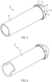
- FIG. 3 is a perspective view of the core mandrel 26.
- the core mandrel 26 includes a body 36 and a cap 38.
- the cap 38 can include the shutoff surfaces 23, and in some embodiments, the shutoff surfaces 23 can form channels 25.
- the body 36 can be hollow, and in some embodiments, the body 36 can be solid.
- the body 36 and the cap 38 can be integrally formed together as a solid monolithic part, and in some embodiments, the cap 38 can be solvent bonded to the body 36. For example, as seen in FIG.
- the cap 38 can include a tubular member 40 with a same approximate length as the body 36 that is secured inside of the body 36. However, as seen in FIG. 5 , in some embodiments, the cap 38 can be secured to an end of the body 36 without the tubular member 40.
- materials with a high dielectric constant such as Acrylonitrile Butadiene Styrene, nylon, and ceramic
- materials with a lower dielectric constant such as Polycarbonate, Fluorinated ethylene propylene, and polytetrafluoroethylene, can be used.
- FIG. 6 is a cross-sectional of a portion of the antenna module 22.
- the core mandrel 26 includes a lip 42 that extends over a top of a portion of the thin film RF element 28 and the HBTRT layer 30 to secure the portion of the thin film element 28 and the HBTRT layer 30 between the body and the lip 42.
- the lip 42 can prevent the polymer adhesive hybrid resin that is used to form the outer layer 24 from flowing onto an underside of the thin film RF element 28.
- the over-molded thin film antenna device 20 can include an active component.
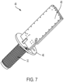
- FIG. 7 is a perspective view of an active RF element 44 of the over-molded thin film antenna device 20 according to disclosed embodiments.
- the active RF element 44 can include a printed circuit board 46 electrically coupled to the RF connector 32 and a LNA circuit 48 electrically coupled to the printed circuit board 46.
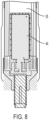
- the active RF element 44 can be housed inside of the core mandrel 26, and in these embodiments, the thin film RF element 28 can be electrically coupled to the RF connector 32 via the printed circuit board 46 and the LNA circuit 48.
- the over-molded thin film antenna device 20 can include a passive component.
- a microstrip line can couple the thin film RF element 32 directly to the RF connector 32.
- FIG. 9 is a perspective view of the antenna module 22 in a one half of a mold 50 according to disclosed embodiments. As seen in FIG. 9 , when the antenna module 22 is placed in the mold 50, the shutoff surfaces 23 can seal against a surface of the mold 50 to hold the antenna module 22 in a concentric relationship with a cavity of the mold.
- the polymer adhesive hybrid resin can be injected into the mold 50 such that the polymer adhesive hybrid resin can flow in a direction indicated by arrows A over the thin film RF element 28 while simultaneously refraining from flowing onto the underside of the thin film RF element 28.
- the polymer adhesive hybrid resin can transform the antenna module 22 and the thin film RF element 28 into the over-molded thin film antenna device 20 as shown in FIG. 1 .
- the polymer adhesive hybrid resin can be injected into the mold 50 at a top center of the core mandrel 26.
- the shutoff surfaces 23 can direct a flow of the polymer adhesive hybrid resin over the thin film RF element 28.
- the base cap 34 can act as one of the shutoff surfaces 23 with respect to the mold 50 to prevent the polymer adhesive hybrid resin from flowing outside of the mold 50 while the polymer adhesive hybrid resin solidifies.
- the lip 42 can prevent the polymer adhesive hybrid resin from flowing onto the underside of the thin film RF element 28 during such a molding process.
- the lip 42 can position and constrain the thin film RF element 28 securely against itself in response to increasing pressure and temperature in the mold 50, which can control the flow of the polymer adhesive hybrid resin around the shutoff surfaces 23 and through the channels 25, thereby uniformly establish an over molded geometry of the over-molded thin film antenna device 20.
Landscapes
- Engineering & Computer Science (AREA)
- Microelectronics & Electronic Packaging (AREA)
- Power Engineering (AREA)
- Manufacturing & Machinery (AREA)
- Mechanical Engineering (AREA)
- Details Of Aerials (AREA)
Description
- The present invention relates generally to radio frequency (RF) communications hardware. More particularly, the present invention relates to an over-molded thin film antenna device.
- Thin film RF elements are commonly used in antenna designs and offer versatility, cost effectiveness, heat resistance, flexibility, and conformability. However, the flexibility and the conformability of the thin film RF elements can limit their use in rugged end use applications that require protection from dynamic shock and vibration and/or that require compact designs with limited space for fasteners. Typical solutions to these problems include encapsulating the thin film RF elements using long cure multipart potting compounds, expandable foams, or conventional molding processes. However, conventional molding processes tend to have a low yield due to increased resin processing pressures and heat exposure of the thin film RF elements and inner electrical elements. Furthermore, expandable foams can absorb moisture and tend to have high dielectric loading of the thin film RF elements, thereby degrading product performance.
-
EP1069647 discloses an antenna having a helical antenna element of a helical shape, in which the helical antenna element is mounted on a flexible substrate rounded to form a cylindrical shape. The helical antenna element has a plurality of oblique conductive patterns extending along the flexible substrate and electrically connected to one another at their terminal ends to form the helical shape.EP1076378 discloses a helical antenna including an element, a feeder circuit, and a connector that connects the element and feeder circuit. The element includes a cylindrical member composed of a dielectric and a plurality of radiation elements that are provided in helical form at intervals on the outer surface of this cylindrical member. The feeder circuit is mounted on a circuit board that is arranged below the cylindrical member. The connector is arranged between the circuit board and the cylindrical member and is composed of an insulating material that is provided in a solid unit with connection pins that electrically connect the ends of the radiation elements to the circuit board.GB2322236 - In view of the above, there is a continuing, ongoing need for improved antenna systems.
- The present invention is defined in the independent claims. Optional features are defined in the dependent claims.
-
-
FIG. 1 is a perspective view of an over-molded thin film antenna device according to disclosed embodiments; -
FIG. 2 is a perspective view of an antenna module of an over-molded thin film antenna device according to disclosed embodiments; -
FIG. 3 is a perspective view of a core mandrel of an over-molded thin film antenna device according to disclosed embodiments; -
FIG. 4 is a perspective view of a portion of a core mandrel of an over-molded thin film antenna device according to disclosed embodiments; -
FIG. 5 is a perspective view of a core mandrel of an over-molded thin film antenna device according to disclosed embodiments; -
FIG. 6 is a cross-sectional view of a portion of an antenna module of an over-molded thin film antenna device according to disclosed embodiments; -
FIG. 7 is a perspective view of an active RF element of an antenna module of an over-molded thin film antenna device according to disclosed embodiments; -
FIG. 8 is a cross-sectional view of a portion of an over-molded thin film antenna device according to disclosed embodiments; and -
FIG. 9 is a perspective view of an antenna module of an over-molded thin film antenna device in a mold according to disclosed embodiments. - While this invention is susceptible of an embodiment in many different forms, there are shown in the drawings and will be described herein in detail specific embodiments thereof with the understanding that the present disclosure is to be considered as an exemplification of the principles of the invention. It is not intended to limit the invention to the specific illustrated embodiments.
- Embodiments disclosed herein include a ruggedized over-molded thin film antenna device for RF applications that includes a thin film RF element, e.g. in a helical or quadrifilar formation formed into a cylindrical shape, over a hollow or solid support core mandrel around which the thin film RF element is wrapped such that the cylindrical core mandrel supports a substrate of the thin film RF element. Embodiments disclosed herein also include an antenna module that includes a core support that holds the cylindrical core mandrel and the thin film RF element and that can precisely control a material flow of an over-molding hybrid polymer adhesive resin during a molding process to encompass the cylindrical core mandrel and the thin film RF antenna element with the over-molding hybrid polymer adhesive resin, thereby ruggedizing the thin film RF element.
- In some embodiments, the substrate of the thin film RF element can vary in physical, mechanical, and electrical properties to suit a variety of antenna applications and operational frequencies. Furthermore, in some embodiments, the thin film RF element can include a metalized region on a first side thereof and a grounding band laminated to a second side thereof, opposite the first side. When wrapped onto the cylindrical core mandrel, in some embodiments, a resulting geometry of the thin film RF element can be held in place on the cylindrical core mandrel with a band of high bond temperature resistant tape (HBTRT), such as Kapton, and ground trace soldering. Further still, in some embodiments, the thin film RF element on the cylindrical core mandrel can be installed onto a base that interfaces with an RF connector and can be grounded to the base by soldering or conducting tape wrap.
- The ruggedized over-molded thin film antenna device described herein can be constructed for use as either a passive device or an active device. As the passive device, the thin film RF element can be fed and routed to the RF connector via a coaxial cable or other suitable method, such as a microstrip line. However, as the active device, the thin film RF element can be soldered to a base PCB carrier or the base itself and fed by the microstrip line to a low noise amplifier (LNA) circuit that can be housed within an available volume of the cylindrical core mandrel. In any embodiment, a connector end of the ruggedized over-molded thin film antenna device can be adjusted to accommodate a wide range of possible connections and customization options for a multitude of mounting and RF interfaces.
- In some embodiments, a head or other top geometric features of the cylindrical core mandrel can overlap the thin film RF element to prevent the over-molding hybrid polymer adhesive resin from infiltrating between an underside of the thin film RF element and the cylindrical core mandrel, for example, during the molding process. In some embodiments, the head or the other top geometric features can be part of a shutoff cap component that is separate from the cylindrical core mandrel, but can be solvent bonded to a body of the cylindrical core mandrel to establish the material flow of the over-molding hybrid polymer adhesive resin at a gate of a mold that facilitates the molding process.
- The cylindrical core mandrel includes shutoff surfaces that seal against a surface of the mold such that the cylindrical core mandrel can be held in a precise concentric relationship relative to the mold. A cavity of the mold can define a final geometry of the ruggedized over-molded thin film antenna device. Accordingly, the shutoff surfaces of the cylindrical core mandrel and the precise concentric relationship between the cylindrical core mandrel and the mold can ensure that the material flow of the over-molding hybrid polymer adhesive resin around the thin film RF element is uniform. For example, in some embodiments, the mold can be designed to receive the over-molding hybrid polymer adhesive resin (e.g. a Polymer-Adhesive) that is injected into the mold near a top center of the cylindrical core mandrel. In this manner, a combination of the mold, the mating surfaces of the cylindrical core mandrel, and the precise concentric relationship therebetween can result in an efficient, repeatable, and balanced low pressure over-molding (LPOM) cycle that can produce a robust and durable sealed device with predictable RF performance without any need for additional fasteners.
-
FIG. 1 is a perspective view of an over-molded thinfilm antenna device 20 according to disclosed embodiments. As seen inFIG. 1 , the over-molded thinfilm antenna device 20 includes anantenna module 22 covered by anouter layer 24 that is molded betweenshutoff surfaces 23 of theantenna module 22. In some embodiments, theouter layer 24 can include a solidified polymer adhesive hybrid resin, and in some embodiments, theouter layer 24 can protect internal electrical components and RF structures of the over-molded thinfilm antenna device 20, for example, from moisture ingress, excessive molding pressures, and damaging heat exposure. Furthermore, in some embodiments, theouter layer 24 can provide a robust, durable housing without any need for mechanical fasteners. -
FIG. 2 is a perspective view of theantenna module 22 without theouter layer 24. As seen inFIG. 2 , theantenna module 22 includes acore mandrel 26 and a thinfilm RF element 28 wrapped around and supported by thecore mandrel 26. In some embodiments, aHBTRT layer 30 and ground trace soldering can secure the thinfilm RF element 28 to thecore mandrel 26. Furthermore, as seen inFIG. 2 , theantenna module 22 includes anRF connector 32 electrically coupled to the thinfilm RF element 28, and in some embodiments, abase cap 34 can surround theRF connector 34 and an end of thecore mandrel 26. -
FIG. 3 is a perspective view of thecore mandrel 26. As seen inFIG. 3 , thecore mandrel 26 includes abody 36 and acap 38. In some embodiments, thecap 38 can include theshutoff surfaces 23, and in some embodiments, theshutoff surfaces 23 can formchannels 25. In some embodiments, thebody 36 can be hollow, and in some embodiments, thebody 36 can be solid. Furthermore, in some embodiments, thebody 36 and thecap 38 can be integrally formed together as a solid monolithic part, and in some embodiments, thecap 38 can be solvent bonded to thebody 36. For example, as seen inFIG. 4 , in some embodiments, thecap 38 can include a tubular member 40 with a same approximate length as thebody 36 that is secured inside of thebody 36. However, as seen inFIG. 5 , in some embodiments, thecap 38 can be secured to an end of thebody 36 without the tubular member 40. - Various materials are contemplated for the
core mandrel 26. For example, in some embodiments, materials with a high dielectric constant, such as Acrylonitrile Butadiene Styrene, nylon, and ceramic, can be used. Additionally or alternatively, in some embodiments, materials with a lower dielectric constant, such as Polycarbonate, Fluorinated ethylene propylene, and polytetrafluoroethylene, can be used. -
FIG. 6 is a cross-sectional of a portion of theantenna module 22. As seen inFIG. 6 , thecore mandrel 26 includes alip 42 that extends over a top of a portion of the thinfilm RF element 28 and theHBTRT layer 30 to secure the portion of thethin film element 28 and theHBTRT layer 30 between the body and thelip 42. When theouter layer 24 is over molded onto theantenna module 22, thelip 42 can prevent the polymer adhesive hybrid resin that is used to form theouter layer 24 from flowing onto an underside of the thinfilm RF element 28. - In some embodiments, the over-molded thin
film antenna device 20 can include an active component. For example,FIG. 7 is a perspective view of anactive RF element 44 of the over-molded thinfilm antenna device 20 according to disclosed embodiments. As seen inFIG. 7 , in some embodiments, theactive RF element 44 can include a printedcircuit board 46 electrically coupled to theRF connector 32 and aLNA circuit 48 electrically coupled to the printedcircuit board 46. As seen inFIG. 8 , in some embodiments, theactive RF element 44 can be housed inside of thecore mandrel 26, and in these embodiments, the thinfilm RF element 28 can be electrically coupled to theRF connector 32 via the printedcircuit board 46 and theLNA circuit 48. - However, in some embodiments, the over-molded thin
film antenna device 20 can include a passive component. For example, in these embodiments, a microstrip line can couple the thinfilm RF element 32 directly to theRF connector 32. -
FIG. 9 is a perspective view of theantenna module 22 in a one half of amold 50 according to disclosed embodiments. As seen inFIG. 9 , when theantenna module 22 is placed in themold 50, the shutoff surfaces 23 can seal against a surface of themold 50 to hold theantenna module 22 in a concentric relationship with a cavity of the mold. - In operation, the polymer adhesive hybrid resin can be injected into the
mold 50 such that the polymer adhesive hybrid resin can flow in a direction indicated by arrows A over the thinfilm RF element 28 while simultaneously refraining from flowing onto the underside of the thinfilm RF element 28. When solidified, the polymer adhesive hybrid resin can transform theantenna module 22 and the thinfilm RF element 28 into the over-molded thinfilm antenna device 20 as shown inFIG. 1 . - In some embodiments, the polymer adhesive hybrid resin can be injected into the
mold 50 at a top center of thecore mandrel 26. Furthermore, in some embodiments, the shutoff surfaces 23 can direct a flow of the polymer adhesive hybrid resin over the thinfilm RF element 28. Similarly, in some embodiments, thebase cap 34 can act as one of the shutoff surfaces 23 with respect to themold 50 to prevent the polymer adhesive hybrid resin from flowing outside of themold 50 while the polymer adhesive hybrid resin solidifies. - Further still, in some embodiments, the
lip 42 can prevent the polymer adhesive hybrid resin from flowing onto the underside of the thinfilm RF element 28 during such a molding process. For example, in some embodiments, thelip 42 can position and constrain the thinfilm RF element 28 securely against itself in response to increasing pressure and temperature in themold 50, which can control the flow of the polymer adhesive hybrid resin around the shutoff surfaces 23 and through thechannels 25, thereby uniformly establish an over molded geometry of the over-molded thinfilm antenna device 20. - Although a few embodiments have been described in detail above, other modifications are possible. For example, other components may be added to or removed from the described systems, and other embodiments may be within the scope of the invention.
- From the foregoing, it will be observed that numerous variations and modifications may be effected without departing from the scope of the invention as defined in the claims. It is, of course, intended to cover all such modifications as fall within the scope of the claims.
Claims (15)
- An antenna device (20) comprising:a core mandrel (26) having a body (36) and a lip (42);a thin film radio frequency -RF- antenna element (28) wrapped around and supported by the body (36), wherein the lip (42) extends over a top of a portion of the thin film RF antenna element (28) to secure the portion of the thin film RF antenna element (28) between the body (36) and the lip (42);an RF connector (32) electrically coupled to the thin film RF antenna element (28); andan outer layer (24) molded between shutoff surfaces (23) of the core mandrel (26) and over the thin film RF antenna element (28).
- The antenna device of claim 1 further comprising:a printed circuit board (46) electrically coupled to the RF connector (32); anda low noise amplifier circuit (48) electrically coupled to the printed circuit board (46),wherein the low noise amplifier circuit (48) is housed inside of the core mandrel (26), andwherein the thin film RF antenna element (28) is electrically coupled to the RF connector (32) through the printed circuit board (46) and the low noise amplifier circuit (48).
- The antenna device of claim 1 or 2 further comprising:
a microstrip line coupling the thin film RF antenna element (28) directly to the RF connector (32). - The antenna device of claim 1, 2 or 3 further comprising:
a high bond temperature resistant tape layer (30) and ground trace soldering securing the thin film RF antenna element (28) to the body (36). - The antenna device of any one of claims 1 to 4 further comprising:a cap (38) of the core mandrel (26) solvent bonded to the body (36),wherein the cap (38) includes the lip (42) and at least some of the shutoff surfaces (23).
- The antenna device of any one of claims 1 to 5 wherein the body (36) is hollow.
- The antenna device of any one of claims 1 to 5 wherein the body (36) is solid.
- The antenna device of any preceding claim wherein the core mandrel (26) is one of Acrylonitrile Butadiene Styrene, nylon, ceramic, Polycarbonate, Fluorinated ethylene propylene, or polytetrafluoroethylene.
- The antenna device of any preceding claim wherein the outer layer (24) includes a solidified polymer adhesive hybrid resin.
- The antenna device of any preceding claim further comprising:a base cap (34) surrounding the RF connector (32) and an end of the core mandrel (26),wherein the outer layer (24) is molded over the base cap.
- A method of forming an antenna device according to claim 1, the method comprising:providing an uncoated antenna module (22) that includes a core mandrel (26) and a thin film radio frequency -RF- antenna element (28) wrapped around and supported by the core mandrel (26);inserting the uncoated antenna module into a mold cavity (50); andinjecting a polymer adhesive hybrid resin into the mold cavity (50), directing the polymer adhesive hybrid resin to flow over the thin film RF antenna element (28), and preventing the polymer adhesive hybrid resin from flowing onto an underside of the thin film RF antenna element (28), thereby to transform the uncoated antenna module into an over-molded antenna module (22) after the polymer adhesive hybrid resin solidifies into an outer layer (24).
- The method of claim 11 further comprising:
a lip (42) of the core mandrel (26) that extends over a top of a portion of the thin film RF element (28) securing the portion of the thin film RF antenna element (28) between the lip (42) and a body (36) of the core mandrel (26) and preventing the polymer adhesive hybrid resin from flowing onto the underside of the thin film RF antenna element (28). - The method of claim 12 further comprising:
shutoff surfaces (23) of the core mandrel (26) sealing against a surface of the mold cavity (50) to hold the uncoated antenna module in a concentric relationship with the mold cavity (50) and direct a flow of the polymer adhesive hybrid resin. - The method of claim 13 wherein the core mandrel (26) includes a cap (38) solvent bonded to the body (36), and wherein the cap (38) includes the lip (42) and at least some of the shutoff surfaces (23).
- The method of any one of claims 11 to 14 further comprising:
injecting the polymer adhesive hybrid resin into the mold cavity (50) at a top center of the core mandrel (26).
Applications Claiming Priority (1)
| Application Number | Priority Date | Filing Date | Title |
|---|---|---|---|
| US16/554,080 US11145966B2 (en) | 2019-08-28 | 2019-08-28 | Over-molded thin film antenna device |
Publications (2)
| Publication Number | Publication Date |
|---|---|
| EP3787106A1 EP3787106A1 (en) | 2021-03-03 |
| EP3787106B1 true EP3787106B1 (en) | 2024-05-08 |
Family
ID=71894754
Family Applications (1)
| Application Number | Title | Priority Date | Filing Date |
|---|---|---|---|
| EP20188764.3A Active EP3787106B1 (en) | 2019-08-28 | 2020-07-30 | Over-molded thin film antenna device |
Country Status (5)
| Country | Link |
|---|---|
| US (2) | US11145966B2 (en) |
| EP (1) | EP3787106B1 (en) |
| CN (1) | CN112448149A (en) |
| CA (1) | CA3089229C (en) |
| FI (1) | FI3787106T3 (en) |
Families Citing this family (1)
| Publication number | Priority date | Publication date | Assignee | Title |
|---|---|---|---|---|
| JP7506286B1 (en) * | 2023-12-28 | 2024-06-25 | 株式会社Maruwa | Helical antenna, antenna device and communication device |
Family Cites Families (18)
| Publication number | Priority date | Publication date | Assignee | Title |
|---|---|---|---|---|
| JPH10173421A (en) * | 1996-12-05 | 1998-06-26 | Harada Ind Co Ltd | Rod antenna for portable transceiver |
| FR2759814B1 (en) | 1997-02-14 | 1999-04-30 | Dassault Electronique | PROPELLER HYPERFREQUENCY ANTENNA ELEMENTS |
| CA2197828C (en) * | 1997-02-18 | 2004-05-04 | Normand Dery | Thin-film antenna device for use with remote vehicle starting systems |
| JP3041520B2 (en) * | 1998-01-19 | 2000-05-15 | 株式会社トーキン | antenna |
| SE514568C2 (en) * | 1998-05-18 | 2001-03-12 | Allgon Ab | An antenna device comprising feed means and a hand-held radio communication device for such an antenna device |
| ES2453486T3 (en) * | 1999-03-24 | 2014-04-07 | Motorola Solutions, Inc. | Circuit chip connector and connection method of a circuit chip |
| JP3399513B2 (en) | 1999-08-10 | 2003-04-21 | 日本電気株式会社 | Helical antenna and manufacturing method thereof |
| WO2005029640A1 (en) * | 2003-09-12 | 2005-03-31 | Centurion Wireless Technologies, Inc. | Multi piece puzzle-lock antenna using flex film radiator |
| JP4340905B2 (en) * | 2005-03-10 | 2009-10-07 | ミツミ電機株式会社 | Antenna device |
| US7554509B2 (en) * | 2006-08-25 | 2009-06-30 | Inpaq Technology Co., Ltd. | Column antenna apparatus and method for manufacturing the same |
| JP4770665B2 (en) * | 2006-09-21 | 2011-09-14 | ミツミ電機株式会社 | Antenna device |
| JP4945337B2 (en) * | 2007-06-19 | 2012-06-06 | 株式会社東芝 | Electronics |
| US7927534B1 (en) * | 2009-11-13 | 2011-04-19 | Mercury Plastics, Inc. | Process to make a waterway connector |
| US20120019425A1 (en) * | 2010-07-21 | 2012-01-26 | Kwan-Ho Lee | Antenna For Increasing Beamwidth Of An Antenna Radiation Pattern |
| JP5385886B2 (en) * | 2010-11-02 | 2014-01-08 | Towa株式会社 | Resin sealing molding method and apparatus for electric circuit parts |
| TWI795918B (en) * | 2015-01-15 | 2023-03-11 | 美商Mks儀器公司 | Method of making a gauge |
| US10205216B2 (en) * | 2016-05-06 | 2019-02-12 | GM Global Technology Operations LLC | Thin film antenna to FAKRA connector |
| US20190044236A1 (en) * | 2017-08-02 | 2019-02-07 | Pc-Tel, Inc. | One-piece dual-band antenna and ground plane |
-
2019
- 2019-08-28 US US16/554,080 patent/US11145966B2/en active Active
-
2020
- 2020-07-30 FI FIEP20188764.3T patent/FI3787106T3/en active
- 2020-07-30 EP EP20188764.3A patent/EP3787106B1/en active Active
- 2020-08-06 CA CA3089229A patent/CA3089229C/en active Active
- 2020-08-26 CN CN202010869115.XA patent/CN112448149A/en active Pending
-
2021
- 2021-02-10 US US17/172,547 patent/US11165147B2/en active Active
Also Published As
| Publication number | Publication date |
|---|---|
| US20210167490A1 (en) | 2021-06-03 |
| CA3089229C (en) | 2026-05-19 |
| CN112448149A (en) | 2021-03-05 |
| US11145966B2 (en) | 2021-10-12 |
| CA3089229A1 (en) | 2021-02-28 |
| FI3787106T3 (en) | 2024-05-23 |
| US20210066793A1 (en) | 2021-03-04 |
| EP3787106A1 (en) | 2021-03-03 |
| US11165147B2 (en) | 2021-11-02 |
Similar Documents
| Publication | Publication Date | Title |
|---|---|---|
| US7768461B2 (en) | Antenna device with insert-molded antenna pattern | |
| EP0723737B1 (en) | Computer peripheral cards having a solid one-piece housing and method of manufacturing the same | |
| US8410990B2 (en) | Antenna with integrated RF module | |
| US11013155B2 (en) | Electromagnetic wave shielding structure and manufacturing method therefor | |
| KR20010030375A (en) | Antenna package for a wireless communications device | |
| AU7092098A (en) | A shielding housing and a method of producing a shielding housing | |
| JP2009528717A (en) | Hybrid circuit with integrated antenna | |
| EP1641074B1 (en) | Antenna device | |
| KR100816262B1 (en) | Electronic device housing built-in antenna and manufacturing method thereof | |
| JP5823774B2 (en) | Conductive member and electronic device including the same | |
| US11165147B2 (en) | Over-molded thin film antenna device | |
| CN215813334U (en) | Electronic device, terminal device, and radar | |
| EP1633015B1 (en) | Sealing member and sealing structure of electronic circuit unit | |
| JP7281002B2 (en) | Fully shielded high frequency connectors and connector modules | |
| JP7672410B2 (en) | Laser Direct Structure (LDS) Antenna Assembly | |
| CN105390805A (en) | Radiator frame having antenna pattern embedded therein and method of manufacturing the same | |
| US12567707B2 (en) | Devices, assemblies, and methods for terminating coaxial radiofrequency ports | |
| JP4443851B2 (en) | Planar antenna device | |
| US7151503B2 (en) | Antenna unit | |
| KR20070023878A (en) | Manufacturing method of built-in antenna using built-in antenna and in molding or insert molding | |
| JP2015008392A (en) | Automotive antenna | |
| KR101452060B1 (en) | Connector, tuner using the same and manufacturing method thereof | |
| JP2010041625A (en) | Onboard waterproof antenna apparatus and waterproof molding method thereof | |
| KR20160143622A (en) | Printed board assembly and manufacturing method thereof | |
| CN223218452U (en) | Middle frame assembly and electronic equipment |
Legal Events
| Date | Code | Title | Description |
|---|---|---|---|
| PUAI | Public reference made under article 153(3) epc to a published international application that has entered the european phase |
Free format text: ORIGINAL CODE: 0009012 |
|
| STAA | Information on the status of an ep patent application or granted ep patent |
Free format text: STATUS: THE APPLICATION HAS BEEN PUBLISHED |
|
| AK | Designated contracting states |
Kind code of ref document: A1 Designated state(s): AL AT BE BG CH CY CZ DE DK EE ES FI FR GB GR HR HU IE IS IT LI LT LU LV MC MK MT NL NO PL PT RO RS SE SI SK SM TR |
|
| AX | Request for extension of the european patent |
Extension state: BA ME |
|
| RAP3 | Party data changed (applicant data changed or rights of an application transferred) |
Owner name: PCTEL, INC. |
|
| STAA | Information on the status of an ep patent application or granted ep patent |
Free format text: STATUS: REQUEST FOR EXAMINATION WAS MADE |
|
| 17P | Request for examination filed |
Effective date: 20210902 |
|
| RBV | Designated contracting states (corrected) |
Designated state(s): AL AT BE BG CH CY CZ DE DK EE ES FI FR GB GR HR HU IE IS IT LI LT LU LV MC MK MT NL NO PL PT RO RS SE SI SK SM TR |
|
| STAA | Information on the status of an ep patent application or granted ep patent |
Free format text: STATUS: EXAMINATION IS IN PROGRESS |
|
| 17Q | First examination report despatched |
Effective date: 20230301 |
|
| GRAP | Despatch of communication of intention to grant a patent |
Free format text: ORIGINAL CODE: EPIDOSNIGR1 |
|
| STAA | Information on the status of an ep patent application or granted ep patent |
Free format text: STATUS: GRANT OF PATENT IS INTENDED |
|
| INTG | Intention to grant announced |
Effective date: 20240227 |
|
| GRAS | Grant fee paid |
Free format text: ORIGINAL CODE: EPIDOSNIGR3 |
|
| GRAA | (expected) grant |
Free format text: ORIGINAL CODE: 0009210 |
|
| STAA | Information on the status of an ep patent application or granted ep patent |
Free format text: STATUS: THE PATENT HAS BEEN GRANTED |
|
| AK | Designated contracting states |
Kind code of ref document: B1 Designated state(s): AL AT BE BG CH CY CZ DE DK EE ES FI FR GB GR HR HU IE IS IT LI LT LU LV MC MK MT NL NO PL PT RO RS SE SI SK SM TR |
|
| REG | Reference to a national code |
Ref country code: GB Ref legal event code: FG4D |
|
| REG | Reference to a national code |
Ref country code: CH Ref legal event code: EP |
|
| REG | Reference to a national code |
Ref country code: FI Ref legal event code: FGE |
|
| REG | Reference to a national code |
Ref country code: SE Ref legal event code: TRGR |
|
| REG | Reference to a national code |
Ref country code: DE Ref legal event code: R096 Ref document number: 602020030516 Country of ref document: DE |
|
| REG | Reference to a national code |
Ref country code: IE Ref legal event code: FG4D |
|
| REG | Reference to a national code |
Ref country code: LT Ref legal event code: MG9D |
|
| REG | Reference to a national code |
Ref country code: NL Ref legal event code: MP Effective date: 20240508 |
|
| PG25 | Lapsed in a contracting state [announced via postgrant information from national office to epo] |
Ref country code: IS Free format text: LAPSE BECAUSE OF FAILURE TO SUBMIT A TRANSLATION OF THE DESCRIPTION OR TO PAY THE FEE WITHIN THE PRESCRIBED TIME-LIMIT Effective date: 20240908 |
|
| PG25 | Lapsed in a contracting state [announced via postgrant information from national office to epo] |
Ref country code: BG Free format text: LAPSE BECAUSE OF FAILURE TO SUBMIT A TRANSLATION OF THE DESCRIPTION OR TO PAY THE FEE WITHIN THE PRESCRIBED TIME-LIMIT Effective date: 20240508 |
|
| PG25 | Lapsed in a contracting state [announced via postgrant information from national office to epo] |
Ref country code: HR Free format text: LAPSE BECAUSE OF FAILURE TO SUBMIT A TRANSLATION OF THE DESCRIPTION OR TO PAY THE FEE WITHIN THE PRESCRIBED TIME-LIMIT Effective date: 20240508 |
|
| PGFP | Annual fee paid to national office [announced via postgrant information from national office to epo] |
Ref country code: FI Payment date: 20240712 Year of fee payment: 5 |
|
| PG25 | Lapsed in a contracting state [announced via postgrant information from national office to epo] |
Ref country code: GR Free format text: LAPSE BECAUSE OF FAILURE TO SUBMIT A TRANSLATION OF THE DESCRIPTION OR TO PAY THE FEE WITHIN THE PRESCRIBED TIME-LIMIT Effective date: 20240809 |
|
| PG25 | Lapsed in a contracting state [announced via postgrant information from national office to epo] |
Ref country code: PT Free format text: LAPSE BECAUSE OF FAILURE TO SUBMIT A TRANSLATION OF THE DESCRIPTION OR TO PAY THE FEE WITHIN THE PRESCRIBED TIME-LIMIT Effective date: 20240909 |
|
| REG | Reference to a national code |
Ref country code: AT Ref legal event code: MK05 Ref document number: 1685789 Country of ref document: AT Kind code of ref document: T Effective date: 20240508 |
|
| PG25 | Lapsed in a contracting state [announced via postgrant information from national office to epo] |
Ref country code: NL Free format text: LAPSE BECAUSE OF FAILURE TO SUBMIT A TRANSLATION OF THE DESCRIPTION OR TO PAY THE FEE WITHIN THE PRESCRIBED TIME-LIMIT Effective date: 20240508 |
|
| PG25 | Lapsed in a contracting state [announced via postgrant information from national office to epo] |
Ref country code: ES Free format text: LAPSE BECAUSE OF FAILURE TO SUBMIT A TRANSLATION OF THE DESCRIPTION OR TO PAY THE FEE WITHIN THE PRESCRIBED TIME-LIMIT Effective date: 20240508 |
|
| PGFP | Annual fee paid to national office [announced via postgrant information from national office to epo] |
Ref country code: CH Payment date: 20240801 Year of fee payment: 5 |
|
| PG25 | Lapsed in a contracting state [announced via postgrant information from national office to epo] |
Ref country code: AT Free format text: LAPSE BECAUSE OF FAILURE TO SUBMIT A TRANSLATION OF THE DESCRIPTION OR TO PAY THE FEE WITHIN THE PRESCRIBED TIME-LIMIT Effective date: 20240508 |
|
| PG25 | Lapsed in a contracting state [announced via postgrant information from national office to epo] |
Ref country code: PL Free format text: LAPSE BECAUSE OF FAILURE TO SUBMIT A TRANSLATION OF THE DESCRIPTION OR TO PAY THE FEE WITHIN THE PRESCRIBED TIME-LIMIT Effective date: 20240508 |
|
| PG25 | Lapsed in a contracting state [announced via postgrant information from national office to epo] |
Ref country code: LV Free format text: LAPSE BECAUSE OF FAILURE TO SUBMIT A TRANSLATION OF THE DESCRIPTION OR TO PAY THE FEE WITHIN THE PRESCRIBED TIME-LIMIT Effective date: 20240508 |
|
| PG25 | Lapsed in a contracting state [announced via postgrant information from national office to epo] |
Ref country code: PT Free format text: LAPSE BECAUSE OF FAILURE TO SUBMIT A TRANSLATION OF THE DESCRIPTION OR TO PAY THE FEE WITHIN THE PRESCRIBED TIME-LIMIT Effective date: 20240909 Ref country code: PL Free format text: LAPSE BECAUSE OF FAILURE TO SUBMIT A TRANSLATION OF THE DESCRIPTION OR TO PAY THE FEE WITHIN THE PRESCRIBED TIME-LIMIT Effective date: 20240508 Ref country code: NO Free format text: LAPSE BECAUSE OF FAILURE TO SUBMIT A TRANSLATION OF THE DESCRIPTION OR TO PAY THE FEE WITHIN THE PRESCRIBED TIME-LIMIT Effective date: 20240808 Ref country code: NL Free format text: LAPSE BECAUSE OF FAILURE TO SUBMIT A TRANSLATION OF THE DESCRIPTION OR TO PAY THE FEE WITHIN THE PRESCRIBED TIME-LIMIT Effective date: 20240508 Ref country code: LV Free format text: LAPSE BECAUSE OF FAILURE TO SUBMIT A TRANSLATION OF THE DESCRIPTION OR TO PAY THE FEE WITHIN THE PRESCRIBED TIME-LIMIT Effective date: 20240508 Ref country code: IS Free format text: LAPSE BECAUSE OF FAILURE TO SUBMIT A TRANSLATION OF THE DESCRIPTION OR TO PAY THE FEE WITHIN THE PRESCRIBED TIME-LIMIT Effective date: 20240908 Ref country code: HR Free format text: LAPSE BECAUSE OF FAILURE TO SUBMIT A TRANSLATION OF THE DESCRIPTION OR TO PAY THE FEE WITHIN THE PRESCRIBED TIME-LIMIT Effective date: 20240508 Ref country code: GR Free format text: LAPSE BECAUSE OF FAILURE TO SUBMIT A TRANSLATION OF THE DESCRIPTION OR TO PAY THE FEE WITHIN THE PRESCRIBED TIME-LIMIT Effective date: 20240809 Ref country code: ES Free format text: LAPSE BECAUSE OF FAILURE TO SUBMIT A TRANSLATION OF THE DESCRIPTION OR TO PAY THE FEE WITHIN THE PRESCRIBED TIME-LIMIT Effective date: 20240508 Ref country code: BG Free format text: LAPSE BECAUSE OF FAILURE TO SUBMIT A TRANSLATION OF THE DESCRIPTION OR TO PAY THE FEE WITHIN THE PRESCRIBED TIME-LIMIT Effective date: 20240508 Ref country code: AT Free format text: LAPSE BECAUSE OF FAILURE TO SUBMIT A TRANSLATION OF THE DESCRIPTION OR TO PAY THE FEE WITHIN THE PRESCRIBED TIME-LIMIT Effective date: 20240508 Ref country code: RS Free format text: LAPSE BECAUSE OF FAILURE TO SUBMIT A TRANSLATION OF THE DESCRIPTION OR TO PAY THE FEE WITHIN THE PRESCRIBED TIME-LIMIT Effective date: 20240808 |
|
| PG25 | Lapsed in a contracting state [announced via postgrant information from national office to epo] |
Ref country code: DK Free format text: LAPSE BECAUSE OF FAILURE TO SUBMIT A TRANSLATION OF THE DESCRIPTION OR TO PAY THE FEE WITHIN THE PRESCRIBED TIME-LIMIT Effective date: 20240508 |
|
| PG25 | Lapsed in a contracting state [announced via postgrant information from national office to epo] |
Ref country code: EE Free format text: LAPSE BECAUSE OF FAILURE TO SUBMIT A TRANSLATION OF THE DESCRIPTION OR TO PAY THE FEE WITHIN THE PRESCRIBED TIME-LIMIT Effective date: 20240508 |
|
| PG25 | Lapsed in a contracting state [announced via postgrant information from national office to epo] |
Ref country code: CZ Free format text: LAPSE BECAUSE OF FAILURE TO SUBMIT A TRANSLATION OF THE DESCRIPTION OR TO PAY THE FEE WITHIN THE PRESCRIBED TIME-LIMIT Effective date: 20240508 |
|
| PG25 | Lapsed in a contracting state [announced via postgrant information from national office to epo] |
Ref country code: SK Free format text: LAPSE BECAUSE OF FAILURE TO SUBMIT A TRANSLATION OF THE DESCRIPTION OR TO PAY THE FEE WITHIN THE PRESCRIBED TIME-LIMIT Effective date: 20240508 Ref country code: RO Free format text: LAPSE BECAUSE OF FAILURE TO SUBMIT A TRANSLATION OF THE DESCRIPTION OR TO PAY THE FEE WITHIN THE PRESCRIBED TIME-LIMIT Effective date: 20240508 |
|
| PG25 | Lapsed in a contracting state [announced via postgrant information from national office to epo] |
Ref country code: SM Free format text: LAPSE BECAUSE OF FAILURE TO SUBMIT A TRANSLATION OF THE DESCRIPTION OR TO PAY THE FEE WITHIN THE PRESCRIBED TIME-LIMIT Effective date: 20240508 |
|
| PG25 | Lapsed in a contracting state [announced via postgrant information from national office to epo] |
Ref country code: SM Free format text: LAPSE BECAUSE OF FAILURE TO SUBMIT A TRANSLATION OF THE DESCRIPTION OR TO PAY THE FEE WITHIN THE PRESCRIBED TIME-LIMIT Effective date: 20240508 Ref country code: SK Free format text: LAPSE BECAUSE OF FAILURE TO SUBMIT A TRANSLATION OF THE DESCRIPTION OR TO PAY THE FEE WITHIN THE PRESCRIBED TIME-LIMIT Effective date: 20240508 Ref country code: RO Free format text: LAPSE BECAUSE OF FAILURE TO SUBMIT A TRANSLATION OF THE DESCRIPTION OR TO PAY THE FEE WITHIN THE PRESCRIBED TIME-LIMIT Effective date: 20240508 Ref country code: EE Free format text: LAPSE BECAUSE OF FAILURE TO SUBMIT A TRANSLATION OF THE DESCRIPTION OR TO PAY THE FEE WITHIN THE PRESCRIBED TIME-LIMIT Effective date: 20240508 Ref country code: DK Free format text: LAPSE BECAUSE OF FAILURE TO SUBMIT A TRANSLATION OF THE DESCRIPTION OR TO PAY THE FEE WITHIN THE PRESCRIBED TIME-LIMIT Effective date: 20240508 Ref country code: CZ Free format text: LAPSE BECAUSE OF FAILURE TO SUBMIT A TRANSLATION OF THE DESCRIPTION OR TO PAY THE FEE WITHIN THE PRESCRIBED TIME-LIMIT Effective date: 20240508 |
|
| PG25 | Lapsed in a contracting state [announced via postgrant information from national office to epo] |
Ref country code: MC Free format text: LAPSE BECAUSE OF FAILURE TO SUBMIT A TRANSLATION OF THE DESCRIPTION OR TO PAY THE FEE WITHIN THE PRESCRIBED TIME-LIMIT Effective date: 20240508 Ref country code: IT Free format text: LAPSE BECAUSE OF FAILURE TO SUBMIT A TRANSLATION OF THE DESCRIPTION OR TO PAY THE FEE WITHIN THE PRESCRIBED TIME-LIMIT Effective date: 20240508 |
|
| REG | Reference to a national code |
Ref country code: DE Ref legal event code: R097 Ref document number: 602020030516 Country of ref document: DE |
|
| PLBE | No opposition filed within time limit |
Free format text: ORIGINAL CODE: 0009261 |
|
| STAA | Information on the status of an ep patent application or granted ep patent |
Free format text: STATUS: NO OPPOSITION FILED WITHIN TIME LIMIT |
|
| PG25 | Lapsed in a contracting state [announced via postgrant information from national office to epo] |
Ref country code: LU Free format text: LAPSE BECAUSE OF NON-PAYMENT OF DUE FEES Effective date: 20240730 |
|
| PG25 | Lapsed in a contracting state [announced via postgrant information from national office to epo] |
Ref country code: LU Free format text: LAPSE BECAUSE OF NON-PAYMENT OF DUE FEES Effective date: 20240730 |
|
| 26N | No opposition filed |
Effective date: 20250211 |
|
| PG25 | Lapsed in a contracting state [announced via postgrant information from national office to epo] |
Ref country code: BE Free format text: LAPSE BECAUSE OF NON-PAYMENT OF DUE FEES Effective date: 20240731 Ref country code: SI Free format text: LAPSE BECAUSE OF FAILURE TO SUBMIT A TRANSLATION OF THE DESCRIPTION OR TO PAY THE FEE WITHIN THE PRESCRIBED TIME-LIMIT Effective date: 20240508 |
|
| REG | Reference to a national code |
Ref country code: BE Ref legal event code: MM Effective date: 20240731 |
|
| PGFP | Annual fee paid to national office [announced via postgrant information from national office to epo] |
Ref country code: GB Payment date: 20250605 Year of fee payment: 6 |
|
| PGFP | Annual fee paid to national office [announced via postgrant information from national office to epo] |
Ref country code: FR Payment date: 20250610 Year of fee payment: 6 |
|
| PG25 | Lapsed in a contracting state [announced via postgrant information from national office to epo] |
Ref country code: IE Free format text: LAPSE BECAUSE OF NON-PAYMENT OF DUE FEES Effective date: 20240730 |
|
| PGFP | Annual fee paid to national office [announced via postgrant information from national office to epo] |
Ref country code: SE Payment date: 20250610 Year of fee payment: 6 |
|
| PGFP | Annual fee paid to national office [announced via postgrant information from national office to epo] |
Ref country code: DE Payment date: 20250604 Year of fee payment: 6 |
|
| PG25 | Lapsed in a contracting state [announced via postgrant information from national office to epo] |
Ref country code: CY Free format text: LAPSE BECAUSE OF FAILURE TO SUBMIT A TRANSLATION OF THE DESCRIPTION OR TO PAY THE FEE WITHIN THE PRESCRIBED TIME-LIMIT; INVALID AB INITIO Effective date: 20200730 |
|
| REG | Reference to a national code |
Ref country code: CH Ref legal event code: H13 Free format text: ST27 STATUS EVENT CODE: U-0-0-H10-H13 (AS PROVIDED BY THE NATIONAL OFFICE) Effective date: 20260224 |
|
| PG25 | Lapsed in a contracting state [announced via postgrant information from national office to epo] |
Ref country code: HU Free format text: LAPSE BECAUSE OF FAILURE TO SUBMIT A TRANSLATION OF THE DESCRIPTION OR TO PAY THE FEE WITHIN THE PRESCRIBED TIME-LIMIT; INVALID AB INITIO Effective date: 20200730 |
|
| PG25 | Lapsed in a contracting state [announced via postgrant information from national office to epo] |
Ref country code: FI Free format text: LAPSE BECAUSE OF NON-PAYMENT OF DUE FEES Effective date: 20250730 |
|
| PG25 | Lapsed in a contracting state [announced via postgrant information from national office to epo] |
Ref country code: CH Free format text: LAPSE BECAUSE OF NON-PAYMENT OF DUE FEES Effective date: 20250731 |
|
| PG25 | Lapsed in a contracting state [announced via postgrant information from national office to epo] |
Ref country code: TR Free format text: LAPSE BECAUSE OF FAILURE TO SUBMIT A TRANSLATION OF THE DESCRIPTION OR TO PAY THE FEE WITHIN THE PRESCRIBED TIME-LIMIT Effective date: 20240508 |
|
| PG25 | Lapsed in a contracting state [announced via postgrant information from national office to epo] |
Ref country code: LT Free format text: LAPSE BECAUSE OF FAILURE TO SUBMIT A TRANSLATION OF THE DESCRIPTION OR TO PAY THE FEE WITHIN THE PRESCRIBED TIME-LIMIT Effective date: 20240508 |