EP1076378A2 - Helical antenna with connector and fabrication method of the same - Google Patents
Helical antenna with connector and fabrication method of the same Download PDFInfo
- Publication number
- EP1076378A2 EP1076378A2 EP00306867A EP00306867A EP1076378A2 EP 1076378 A2 EP1076378 A2 EP 1076378A2 EP 00306867 A EP00306867 A EP 00306867A EP 00306867 A EP00306867 A EP 00306867A EP 1076378 A2 EP1076378 A2 EP 1076378A2
- Authority
- EP
- European Patent Office
- Prior art keywords
- connection pins
- connector body
- cylindrical member
- helical antenna
- pins
- Prior art date
- Legal status (The legal status is an assumption and is not a legal conclusion. Google has not performed a legal analysis and makes no representation as to the accuracy of the status listed.)
- Granted
Links
Images









Classifications
-
- H—ELECTRICITY
- H01—ELECTRIC ELEMENTS
- H01Q—ANTENNAS, i.e. RADIO AERIALS
- H01Q23/00—Antennas with active circuits or circuit elements integrated within them or attached to them
-
- H—ELECTRICITY
- H01—ELECTRIC ELEMENTS
- H01Q—ANTENNAS, i.e. RADIO AERIALS
- H01Q11/00—Electrically-long antennas having dimensions more than twice the shortest operating wavelength and consisting of conductive active radiating elements
- H01Q11/02—Non-resonant antennas, e.g. travelling-wave antenna
- H01Q11/08—Helical antennas
-
- H—ELECTRICITY
- H01—ELECTRIC ELEMENTS
- H01Q—ANTENNAS, i.e. RADIO AERIALS
- H01Q5/00—Arrangements for simultaneous operation of antennas on two or more different wavebands, e.g. dual-band or multi-band arrangements
- H01Q5/30—Arrangements for providing operation on different wavebands
- H01Q5/307—Individual or coupled radiating elements, each element being fed in an unspecified way
- H01Q5/342—Individual or coupled radiating elements, each element being fed in an unspecified way for different propagation modes
- H01Q5/357—Individual or coupled radiating elements, each element being fed in an unspecified way for different propagation modes using a single feed point
- H01Q5/364—Creating multiple current paths
- H01Q5/371—Branching current paths
-
- H—ELECTRICITY
- H01—ELECTRIC ELEMENTS
- H01Q—ANTENNAS, i.e. RADIO AERIALS
- H01Q5/00—Arrangements for simultaneous operation of antennas on two or more different wavebands, e.g. dual-band or multi-band arrangements
- H01Q5/40—Imbricated or interleaved structures; Combined or electromagnetically coupled arrangements, e.g. comprising two or more non-connected fed radiating elements
Definitions
- the present invention relates to a helical antenna in which radiation elements are provided in helical form on the surface of a cylindrical member composed of a dielectric, and to a method of manufacturing this helical antenna.
- Helical antennas are used as the antennas for portable terminals in portable telephone systems that employ non-geostationary satellites.
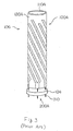
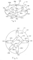
- Fig. 1 is a perspective view of an example of this type of helical antenna of the prior art.
- helical antenna 102 of the prior art is shown that includes element 100, feeder circuit 200, and connection pins 310.
- Element 100 is formed by winding flexible print circuit board 120 in the form of parallel quadrilaterals around dielectric pipe 110.
- Flexible print circuit board 120 is secured to dielectric pipe 110 by an adhesive or a double sided tape.
- Feeder circuit 200 is formed from circuit board 104 (also referred to as a "dielectric board") made up from a disk-shaped dielectric having a larger diameter than dielectric pipe 110. Microstrip lines (not shown in the figure) are formed and a chip-type 4-distributor, resistor, and capacitor are mounted on one surface of dielectric board 104, these components having the function of a 4-distributor/combiner circuit. A ground conductor is formed on the other surface of dielectric board 104. Since this type of feeder circuit is well-known in the art, and functionally, is not an element that is closely connected to the present invention, a detailed explanation of these components is omitted.
- Fig. 2 is a sectional view showing the connection points between element 100 and feeder circuit 200 in helical antenna 102 shown in Fig. 1.
- components identical to those shown in Fig. 1 bear the same reference numerals.
- connection pins 310 are arranged at the edge of element 100.
- Each of connection pins 310 passes through a through-hole formed in dielectric board 104 of feeder circuit 200.
- One end of connection pins 310 is soldered to element 100 and the other is soldered to feeder circuit 200.
- element 100 and dielectric board 104 are connected by inserting connection pins 310 through dielectric board 104, and the outside diameter of feeder circuit 200 is therefore greater than the outside diameter of dielectric pipe 110. This factor is not advantageous for reducing the outside diameter of helical antenna 102.
- An antenna that is incorporated into a portable telephone is preferably as compact as possible, and, for example, a helical antenna of the following construction has been proposed to eliminate the above-described drawback.
- Fig. 3 is a perspective view showing another example of a helical antenna of the prior art.
- constituent elements identical to those of Fig. 1 bear the same reference numerals.
- Helical antenna 106 shown in Fig. 3 includes element 100A, feeder circuit 200A, and connection pins 310.
- Element 100A is formed by winding flexible print circuit board 120A, which is shaped as a parallel quadrilateral, around dielectric pipe 110A.
- the outside diameter of feeder circuit 200A is somewhat larger than the outside diameter of element 100.
- the electrical configuration of feeder circuit 200A is the same as that of feeder circuit 200 shown in Fig. 1.
- Fig. 4 is a sectional view showing in detail the connection points between element 100A and feeder circuit 200A in the helical antenna 106 shown in Fig. 3.
- constituent elements that are the same as those shown in Fig. 3 bear the same reference numerals.
- dielectric pipe 110A The walls of dielectric pipe 110A are thicker on the side of feeder circuit 200A than in other portions of dielectric pipe 110A, and holes for inserting connection pins 310 are formed in this thicker portion of dielectric pipe 110A.
- Flexible print circuit board 120A is wound around dielectric pipe 110A such that its lower end bends inwards at the lower end of dielectric pipe 110A.
- Flexible print circuit board 120A is secured to dielectric pipe 110A by means of an adhesive or a double sided tape.
- connection pins 310 are inserted into the above-described holes in dielectric pipe 110A, and the lower ends are inserted into through-holes formed in dielectric board 104 of feeder circuit 200A. Connection pins 310 are then connected to feeder circuit 200A by soldering at these through-holes. The upper ends of connection pins 310, on the other hand, are soldered to the end of flexible print circuit board 120A that is bent inside dielectric pipe 110A.
- This helical antenna 106 allows each of connection pins 310 to be provided at points closer to the center of dielectric board 104 than in helical antenna 102 shown in Fig. 1, and the outside diameter of feeder circuit 200A can therefore be made smaller than that of feeder circuit 200 shown in Fig. 1.
- this helical antenna 106 has the drawback that the process of winding flexible print circuit board 120A around dielectric pipe 110A is complicated by the necessity of bending the lower end of flexible print circuit board 120A inside the lower end of dielectric pipe 110A.
- a further drawback is the increased number of fabrication steps required for forming holes in dielectric pipe 110A for inserting
- the helical antenna according to the present invention comprises a plurality of radiation elements provided in helical form that are spaced at intervals from each other on the outer surface of a cylindrical member that is composed of a dielectric, a circuit board on which is mounted a feeder circuit for supplying high-frequency energy to the radiation elements, and a connector for electrically connecting the radiation elements and the circuit board.
- the circuit board is arranged below the cylindrical member, and the connector is arranged between the lower end of the cylindrical member and the circuit board.
- the connector is composed of an insulating material and is provided as a solid unit with a plurality of connection pins that electrically connect the end of each radiation element with the circuit board.
- the connector includes a connector body, and the plurality of connection pins are provided on the connector body.
- the connector body includes a lower portion that is formed with an outside diameter that is substantially equal to the outside diameter of the cylindrical member and an upper portion that is formed with an outside diameter that allows insertion inside the cylindrical member with substantially no gap.
- the lower ends of the connection pins protrude downward from the lower surface of the lower portion of the connector body.
- the upper ends of the connection pins protrude upward from the lower portion of connector body with a gap between the connection pins and the outer surface of the upper portion of the connector body.
- the connector body is then joined to the cylindrical member by inserting the upper portion of the connector body into the lower end of the cylindrical member and interposing the lower end of the cylindrical member between the outer surface of the upper portion of the connector body and the upper ends of the connection pins.
- the upper ends of the connection pins are thus electrically-connected to the ends of the radiation elements, and moreover, the lower ends of the connection pins are electrically connected to the circuit board.
- a cylindrical member, a circuit board, and a connector composed of an insulating material are prepared beforehand.
- a plurality of helical radiation elements are provided at intervals on the outer surface of the cylindrical member.
- a feeder circuit for supplying high-frequency energy to the radiation elements is mounted on the circuit board.
- a plurality of connection pins for electrically-connecting the ends of the radiation elements to the circuit board are provided as a solid unit with the connector. Then, the connector is installed on the circuit board and the connection pins are electrically connected to the feeder circuit, and in addition, the connector is attached to the lower end of the cylindrical member and the connection pins are electrically connected to the ends of the radiation elements.
- the connector includes a connector body composed of an insulating material, and the plurality of connection pins are provided as a solid unit with this connector body.
- the lower ends of the connection pins protrude downward from the lower surface of the lower portion of the connector body.
- the upper ends of the connection pins protrude upward from the lower portion of the connector body and form a gap with respect to the outer surface of the upper portion of the connector body.
- the connector body and cylindrical member are then joined by inserting the upper portion of the connector body into the lower end of the cylindrical member and interposing the lower end of the cylindrical member between the upper ends of the connection pins and the outer surface of the upper portion of the connector body, thereby electrically-connecting the upper ends of the connection pins and the ends of the radiation elements, and further, electrically-connecting the lower ends of the connection pins to the circuit board.
- a connector body provided as a solid unit with connection pins is of a construction that includes a lower portion that is formed with substantially the same outside diameter as the outside diameter of a cylindrical member and an upper portion that is formed with an outside diameter that allows insertion inside the cylindrical member with substantially no gap; the lower ends of the connection pins are configured to protrude from the lower surface of the lower portion of the connector body, and the upper ends of the connection pins are configured to extend upward from the lower portion of the connector body such that a gap is formed between the upper ends of the connection pins and the outer surface of the upper portion of the connector body; whereby the diameter of the circuit board can be made equal to or less than the outside diameter of the cylindrical member.
- the diameter of the connector can also be made substantially equal to the diameter of the cylindrical member.
- the cylindrical member and circuit board need only be connected by way of the connector.
- the connector body includes an upper portion and lower portion as described hereinabove and the upper ends of the connection pins are constructed as described hereinabove enables the radiation elements to be electrically-connected to the connection pins by inserting the upper portion of the connector body into the lower end of the cylindrical member and interposing the ends of the radiation elements between the upper ends of the connection pins and the outer surface of the upper portion of the connector body.
- the ends of the radiation elements and the upper ends of the connection pins may also be soldered together as necessary.
- the radiation elements are constituted by metal foil patterns formed on a dielectric sheet
- the radiation elements can be provided in helical form on the outer surface of the cylindrical member by wrapping the dielectric sheet around a cylindrical member.
- adopting a construction in which the radiation elements are interposed between the outer surface of the upper portion of the connector body and the upper ends of the connection pins as described above eliminates the need for bending the lower end of the dielectric sheet toward the center of cylindrical member, as in the prior art, and further, eliminates the need to form holes for inserting connection pins in the end surface of the cylindrical member.
- One form of a fabrication method of a helical antenna of the invention comprises the steps of:
- the step of preparing the connector may include forming a connector body from an insulating material in a shape having a lower portion that has an outside diameter that is substantially equal to the outside diameter of the cylindrical member and an upper portion that has an outside diameter that allows insertion into the cylindrical member with substantially no gap.
- the step of preparing the connector may include: causing the lower ends of each of the connection pins to protrude from the lower surface of the lower portion of the connector body, and causing the upper ends of each of the connection pins to protrude upward from the lower portion of the connector body with a gap between the upper ends of each of the connection pins and the outer surface of the upper portion of the connector body.
- the step of electrically connecting the ends of the radiation elements and each of the connection pins may include joining the connector and the cylindrical member by inserting the upper portion of the connector body into the lower end of the cylindrical member and interposing the lower end of the cylindrical member between the outer surface of the upper portion of the connector body and the upper ends of the connection pins.
- the step of electrically connecting the feeder circuit and each of the connection pins may include: arranging the feeder circuit below the connector, and electrically connecting the lower ends of each of the connection pins to the circuit board.
- Another form of a fabrication method of a helical antenna of the invention comprises the steps of:
- the step of preparing the connector may include positioning the parts of the lower ends of said connection pins that protrude from the lower surface of the lower portion of the connector body closer to the center in the radial direction of the connector body than the upper ends of the connection pins.
- the step of preparing said circuit board may include forming a plurality of through-holes along the edge of the circuit board that are each electrically connected to the feeder circuit; and the step of electrically connecting the feeder circuit and the lower ends of each of the connection pins may include inserting the lower ends of each of the connection pins through a respective one of the through-holes.
- the step of preparing the connector may include forming the upper ends of each of the connection pins such that the upper ends of the connection pins each protrude from the outer surface of the lower portion of the connector body and extend upward along the outer surface of the upper portion of the connector body.
- the step of preparing the connector may include configuring the parts of the upper ends of each of the connection pins that extend upward along the outer surface of the upper portion of said connector body such that each presses elastically against the end of a respective one of the radiation elements; and, the step of electrically connecting the ends of the radiation elements to the upper ends of each of the connection pins may include causing the upper ends of each of the connection pins to press against the end of a respective one of each of the radiation elements.
- the step of preparing the connector may include forming the upper ends of each of the connection pins such that the upper end of each connection pin splits into two upper end pins; and, the step of electrically connecting the ends of the radiation elements to the upper ends of each of the connection pins may include electrically-connecting each of the upper end pins, that have been split into two pins to a different one of the radiation elements.
- the step of preparing the connector may include forming each of the connection pins in substantially a Y-shape composed of the two upper end pins and one lower portion that is connected in common to the bottom portions of the two upper pins.
- the step of preparing said cylindrical member may include constructing each of said radiation elements from a first and a second radiation element that each extends substantially parallel to the other; and the step of electrically-connecting the ends of the radiation elements to each of the connection pins may include connecting one of the two upper end pins to the first radiation element and connecting the other of the two upper end pins to the second radiation element.
- the step of preparing the connector may include forming each of the connection pins by including the steps of:
- the step of preparing the cylindrical member may include constructing each of the radiation elements from a first and a second radiation element that each extends substantially parallel to the other, and a radiation element base that connects said first and second radiation elements at the lower end of said cylindrical member; and, the step of electrically-connecting the ends of the radiation elements and each of the connection pins may include electrically-connecting each of the connection pins to a respective one of the radiation element bases.
- the step of preparing the cylindrical member may include: forming metal foil patterns that constitute the radiation elements on the surface of a dielectric sheet, and winding the dielectric sheet onto the outer surface of the cylindrical member.
- the step of preparing the cylindrical member may include forming the dielectric sheet as a sheet that is substantially a parallelogram in shape, and winding the dielectric sheet onto the outer surface of the cylindrical member in helical form.
- the step of preparing the cylindrical member may include:
- the step of preparing the cylindrical member may further include forming a turned-back portion on the tip of each of the securing pins to prevent dislodging of the securing pins from the through-holes.
- the step of preparing the cylindrical member may include constructing the radiation elements from metal foil patterns that are formed on the outer surface of the cylindrical member by Molded Interconnect Device methods.
- the number of said radiation elements may be at least four.
- the present invention therefore enables easy, reliable, and speedy assembly of a helical antenna without need for special methods.
- the terms “upper” and “lower” that are used in the present invention indicate “up” and “down” when the helical antenna is in an erect state in which the feeder circuit is positioned below the cylindrical member, and do not necessarily indicate “up” or “down” when the helical antenna is in use or when the helical antenna is being assembled.
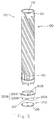
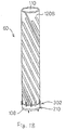
- this helical antenna 20 comprises element 100, feeder circuit 210, and connectors 300 for connecting element 100 and feeder circuit 210.
- Element 100 is formed by winding flexible print circuit board 120 (a dielectric sheet) around the outer surface of cylindrical dielectric pipe 110 (a cylindrical member) and securing with an adhesive or a double-sided tape.
- Materials such as polycarbonate, Teflon (registered trademark of Dupont), PTFE (polytetrafluoroethylene), and ABS may be applied as the material of dielectric pipe 110.
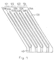
- flexible print circuit board 120 is constituted by a parallel quadrilateral.
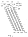
- Y-shaped elongated copper foil patterns 121, 122, 123, and 124 (radiation elements) composed of first copper foil patterns 121A-124A and second copper foil patterns 121B-124B are formed at intervals on the surface of flexible print circuit board 120 and substantially parallel to each other.
- Copper foil patterns 121, 122, 123, and 124 form a helix when flexible print circuit board 120 is wound onto dielectric pipe 110, as shown in Fig. 5.
- a material such as polyimide may be applied as the material of flexible print circuit board 120.
- a first copper foil pattern and a second copper foil pattern of each copper foil pattern are connected at one end, this point forming base 40 (radiation element base) that exhibits a Y-shape.
- feeder circuit 210 has disk-shaped dielectric board 108 of approximately the same diameter as dielectric pipe 110.
- through-holes 108A that pass through dielectric board 108 in the direction of thickness are provided at points along the edge of dielectric board 108 that correspond to lower ends 310A of connection pins 310 (to be described below), these lower ends 310A being inserted through these through-holes 108A.
- one through-hole 108B through which passes a connection pin (not shown) that is connected to a transmitting/receiving circuit (not shown), is provided in dielectric board 108 in the direction of thickness of dielectric board 108.
- Chip-type 4-distributor/combiner circuit 108C is provided on lower surface 1081 of dielectric board 108.
- This 4-distributor/combiner circuit 108C is provided with four antenna-side connection ports 108C1 and one input/output port 108C2.
- Microstrip lines 108D1 that connect each antenna-side connection port 108C1 to a respective through-hole 108A and microstrip line 108D2 that connects input/output port 108C2 and through-hole 108B are formed on lower surface 1081 of dielectric board 108.
- a ground conductor is formed on the upper surface of dielectric board 108, i.e., the surface that confronts element 100.
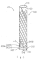
- connector 300 that makes up a part of helical antenna 20 of Fig. 5 is described.
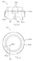
- Connector 300 includes connection pins 310 and ring 300A that is composed of plastic resin and that constitutes the connector body.
- Lower portion 300B of ring 300A is formed with an outside diameter that is substantially equal to the outside diameter of dielectric pipe 110, and upper portion 300C of ring 300A is formed with an outside diameter that allows insertion into dielectric pipe 110 with substantially no gap.
- connection pins 310 protrude downward from the lower surface of lower portion 300B of ring 300A, and upper ends 310B protrude upward from lower portion 300B of ring 300A so as to form a gap between upper ends 310B and the outside surface of upper portion 300C of ring 300A.
- upper ends 310B of connection pins 310 protrude from the outer surface of lower portion 300B of ring 300A and extend upward along the outer surface of upper portion 300A. The middle portions of connection pins 310 therefore are buried inside lower portion 300B of ring 300A.
- connection pins 310 are bent in the middle portion such that lower ends 310A protrude from the lower surface of lower portion 300B of ring 300A at points that closer to the center in the radial direction of ring 300A than upper ends 310B.
- connection pins 310 as a solid unit with ring 300A is next described.
- a metal plate of, for example, brass is first punched out by a sheet metal processing method to form bar piece 311A of the shape shown in Fig. 12.
- This bar piece 311A is shaped by a bending process to form die insert piece 311B as shown in Fig. 13.
- This die insert piece 311B is next preset in a prescribed position of a forming die for forming ring 300A, and insert forming of die insert piece 311B is carried out, whereby die insert piece 311B is formed as a solid piece with the plastic resin that constitutes ring 300A.
- connection pins 310 After forming, the unnecessary parts of the upper portion and lower portion of die insert piece 311B are cut off, and the remaining portions become the four independent connection pins 310.
- the use of brass as the material for connection pins 310 as described above is preferable because brass facilitates soldering.
- upper portion 300C of ring 300A is inserted into the lower end of dielectric pipe 110, the lower end of dielectric pipe 110 is held between the outer surface of upper portion 300C of ring 300A and upper ends 310B of connection pins 310, thereby joining ring 300A to dielectric pipe 110.
- Upper ends 310B of each of connection pins 310 each contact bases 40 of each of copper foil patterns 121-124, thereby establishing electrical connections between each of connection pins 310 and a respective copper foil pattern 121-124.
- upper ends 310B of connection pins 310 are preferably each soldered to bases 40 of copper foil patterns 121-124.
- Lower ends 310A of each of connection pins 310 are electrically connected to feeder circuit 210, which is arranged below connector 300.
- lower ends 310A of connection pins 310 having been inserted through four through-holes 108A that are formed in dielectric board 108 of feeder circuit 210 that is shown in Fig. 8 and Fig. 9, electrically connect with each microstrip line 108D1 by soldering.
- lower ends 310A of connection pins 310 electrically connect by way of each microstrip line 108D1 with antenna-side connection ports 108C1 of 4-distributor/combiner 108C on dielectric board 108.
- connection pins 310 make contact with, and are soldered to bases 40 of copper foil patterns 121-124. Copper patterns 121-124 are thus electrically connected to feeder circuit 210 by way of connection pins 310 of connector 300.
- Fig. 14 is a block diagram showing the configuration of helical antenna of Fig. 5, the electrical operation of helical antenna 20 configured according to the foregoing description is next explained.
- the following explanation pertains to a case in which this helical antenna 20 is used as a satellite telephone antenna that uses a non-geostationary satellite.
- first copper patterns 121A-124A and second copper pattern 121B-124B are set such that first copper foil patterns 121A-124A resonate at a first frequency and second copper foil patterns 121B-124B resonate at a second frequency.
- the first frequency is used as the transmitting band and the second frequency is used as the receiving band.
- the first frequency is set to a lower frequency than the second frequency, and first copper foil patterns 121A-124A are therefore longer than second copper foil patterns 121B-124B.
- the four antenna-side connection ports 108C1 of 4-distributor/combiner circuit 108C are configured to receive and output signals that are of equal amplitude but that differ from each other by 90-degree phase shifts (in the figure, these are shown as 0-degrees, -90 degrees, -180 degrees, and -270 degrees).
- Input/output port 108C2 of 4-distributor/combiner circuit 108C is connected to a transmitting/receiving circuit (not shown in the figure) by way of the connection pin (not shown in the figure) that passes through through-hole 108B (refer to, for example, Fig. 8) and microstrip line 108D2 (refer to, for example, Fig. 8). Transmission signals are received from this transmitting/receiving circuit, and received signals that have been combined by 4-distributor/combiner circuit 108C are outputted to this transmitting/receiving circuit.
- Each of antenna side connection ports 108C1 is connected by the above-described connector 300 to a respective lower end of each of copper foil patterns 121-124.
- 4-distributor/combiner circuit 108C When a high-frequency signal of the first frequency is received at input/output port 108C2 of 4-distributor/combiner circuit 108C from the transmitting/receiving circuit, 4-distributor/combiner circuit 108C distributes the high-frequency signal of the first frequency and outputs to antenna-side connection ports 108C1. At this time, signals that are of equal amplitude but of phases that differ by shifts of 90 degrees are outputted to each of antenna-side connection ports 108C1. Each of the distributed high-frequency signals is received at a respective copper foil pattern 121-124 by way of a respective connection pin 310 of connector 300.
- Each of the high-frequency signals that is received at a copper foil pattern 121-124 resonates at first copper foil pattern 121A-124A of copper foil patterns 121-124, is converted to electromagnetic waves, and is radiated into space.
- the electromagnetic waves that are radiated from the four first copper foil patterns 121A-124A can be combined at a space that is sufficiently separated from this helical antenna 20 to obtain a desired radiation pattern.
- High-frequency signals of the second frequency that are transmitted from a satellite are received at the four second copper foil patterns 121B-124B, and then applied to each of antenna-side connection ports 108C1 of 4-distributor/combiner circuit 108C by way of each of connection pins 310 of connector 300.
- each of the high-frequency signals of the second frequency are of equal amplitude but differ from each other by 90-degree phase shifts.
- 4-distributor/combiner circuit 108C combines these received high-frequency signals of the second frequency and outputs from input/output port 108C2 to the transmitting/receiving circuit.
- the transmitting/receiving circuit then performs a reception process based on the high-frequency signal that is received from input/output port 108C2.
- helical antenna 20 of this embodiment is of a construction in which element 100 and feeder circuit 210 are connected by connector 300, and connector 300 is constructed such that lower ends 310A of connection pins 310 protrude downward from the lower surface of lower portion 300B of ring 300A, and upper ends 310B of connection pins 310 protrude from the outer surface of lower portion 300B of ring 300A and extend upward along this same outer surface.
- the outside diameter of lower portion 300B of connector 300 can therefore be set to substantially the same dimension as the outside diameter of dielectric pipe 110 as described hereinabove.
- connection pins 310 are bent in their middle portions such that the portion of lower ends 310A that protrudes downward from the lower surface of lower portion 300B of ring 300A is positioned more toward the inside of ring 300A in the radial direction of ring 300A than upper ends 310B.
- the outside diameter of dielectric board 108 can be made equal to or smaller than the outside diameter of element 100.
- Helical antenna 20 of this embodiment thus enables a slimmer, i.e., more compact, form.
- the assembly of helical antenna 20 can be realized by inserting connector 300, in which feeder circuit 210 is mounted on lower portion 300B, into the lower end of dielectric pipe 110 such that its upper portion 300C is arranged inside dielectric pipe 110, and then connecting upper ends 310B of each of connection pins 310 to bases 40 of copper foil patterns 121-124 by soldering.
- Helical antenna 20 of this embodiment therefore can be quickly and easily assembled.
- solder was used to connect upper ends 310B of each of connection pins 310 to bases 40 of copper foil patterns 121-124 in the above-described embodiment, a construction that does not require soldering may also be adopted if a connector such as is shown in Fig. 15 is used.
- bent portions 310B1 which are bent in the direction that approaches the outer surface of upper portion 300C, are formed in the portions of upper ends 310B of connection pins 310 that protrude from the outer surface of lower portion of ring 300A and extend upward along the outer surface of upper portion 300B.
- bent portions 310B1 are constructed so as to elastically press against bases 40 of each of copper foil patterns 121-124 when upper portion 300C of connector 300 is inserted into the lower end of dielectric pipe 110.
- connection pins 310 The elastic pressure of bent portions 310B1 of connection pins 310 against bases 40 of each of copper foil patterns 121-124 according to the above-described construction establishes electrical contact between upper ends 310B of connection pins 310 and bases 40 of each of copper foil patterns 121-124 and thus eliminates the need for a soldering step.
- the shape of the copper foil patterns that are formed on the flexible print circuit board that constitutes the helical antenna is not limited to the elongated Y-shaped form such as shown in Fig. 7.
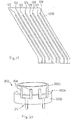
- FIG. 16 A number of examples of the shape of the copper foil patterns that are formed on the flexible print circuit board are shown in Fig. 16 and Fig. 17.
- copper foil patterns 121-124 include first copper foil patterns 121A-124A and second copper foil patterns 121B-124B that extend substantially parallel to each other, and connection points 121C-124C (radiation element bases) that connect the lower ends of both first copper foil patterns 121A-124A and second copper foil patterns 121B-124B.
- Connection points 121C-124C exhibit V shapes with acute bends.
- copper foil patterns 121-124 include first copper foil patterns 121A-124A and second copper foil patterns 121B-124B that extend substantially parallel to each other, and connection points 121C-124C (radiation element bases) that connect the lower ends of both first copper foil patterns 121A-124A and second copper foil patterns 121B-124B.
- Connection points 121C-124C exhibit U shapes with acute bends.
- Connection points 121C-124C of Fig. 16 and Fig. 17 correspond to bases 40 of Fig. 7 and constitute the part that electrically connects to upper ends 310B of connection pins 310.
- helical antenna 60 of the second embodiment of the present invention differs with respect to the first embodiment in regard to the composition of the flexible print circuit board and the construction of the connection pins.
- copper foil patterns 121-128 are formed at fixed intervals with a prescribed angle so as to extend substantially parallel on flexible print circuit board 120B that is used in helical antenna 60 of this embodiment.
- the lengths of copper foil patterns 121-128 are of two varieties, long and the short patterns being alternately arranged.
- connection pins 312 split into two upper end pins 312A as shown in Figs. 20-22.
- Upper end pins 312A protrude from the outer surface of lower portion 300B of ring 300A, extend upward along the outer surface of upper portion 300C of ring 300A and form a gap with the outer surface of upper portion 300C.
- connection pins 312 protrude downward from the lower surface of lower portion 300B of connector 302, similar to connector 300 of the first embodiment.
- each of connection pins 312 exhibits a Y-shaped form with two upper end pins 312A and one lower end.
- each upper end pin 312A is connected to a different copper foil pattern 121-128 on flexible print circuit board 120B by soldering.
- each of upper end pins 312A is provided with a bent portion that is similar to bent portions 310B1 shown in Fig. 15 of the previously described first embodiment, and the elastic pressure of these bent portions against the different copper foil patterns 121-128 on flexible print circuit board 120B establishes electrical contact with upper end pins 312A.
- connection pin in a case in which two copper foil patterns that form a pair are not connected to each other at their end portions as in helical antenna 20 of the first embodiment, the upper end pins of a connection pin can be connected to copper foil patterns that form a pair by forming each of the connection pins in a Y shape as described hereinabove as in the present embodiment to obtain the same effect as the first embodiment.
- connection pins 312 can be fabricated by the same methods as in the first embodiment.
- Connections pin 350 shown in Fig. 23A are formed from a plate member and are configured to have elasticity in the direction of thickness of the plate member.
- Connection pin 350 is made up of upper end portion 350A, middle portion 350B, and lower end portion 350C.
- Lower end portion 350C is configured to protrude downward from the lower surface of lower portion 300B of connector 302.
- Middle portion 350B is bent in the direction of thickness of the plate material that makes up connection pins 350 and connects lower end portion 350C to upper end portion 350A.
- Upper end portion 350A is made up of connection part 350A1 that extends in a direction that is orthogonal to the direction in which lower end portion 350C extends, and two upper end pins 350A2.
- the middle portion of connection part 350A1 is connected to the end portion of middle portion 350B that is opposite lower end portion 350C.
- Upper end pins 350A2 are each formed to extend upward from the two ends of connection part 350A1.
- upper end portion 350A splits into two upper end pins 350A2, and a Y shape is formed by this upper end portion 350A, middle portion 350B, and lower end portion 350C.
- Connection pin 360 shown in Fig. 23B are formed from a rod material and is configured to have elasticity against the direction of bending.
- Connection pin 360 is made up of upper end portion 360A, middle portion 360B, and lower end portion 360C.
- Lower end portion 360C is configured to protrude downward from the lower surface of lower portion 300B of connector 302.
- Middle portion 360B is bent in the direction that crosses the direction in which lower end portion 360C extends and connects lower end portion 360C to upper end portion 360A.
- Upper end portion 360A is made up of connection part 360A1 that extends in a direction that is orthogonal to the direction in which lower end portion 360C extends, and two upper end pins 360A2.
- the middle portion of connection part 360A1 is connected to the end portion of middle portion 360B that is opposite lower end portion 360C.
- Upper end pins 360A2 are each formed to extend upward from the two ends of connection part 360A1.
- upper end portion 360A splits into two upper end pins 360A2, and a Y shape is formed by this upper end portion 360A, middle portion 360B, and lower end portion 360C.
- Connection pin 370 shown in Fig. 23C is formed from a plate member and is constructed to have elasticity in the direction of thickness of the plate member.
- Connection pin 370 is made up of upper end portion 370A, middle portion 370B, and lower end portion 370C.
- Lower end portion 370C is configured to protrude downward from the lower surface of lower portion 300B of connector 302.
- Middle portion 370B is bent in the direction of thickness of the plate member that makes up connection pins 370 and connects lower end portion 370C to upper end portion 370A.
- Upper end portion 370A is made up of connection part 370A1 that extends in a direction that is orthogonal to the direction in which lower end portion 370C extends and two upper end pins 370A2.
- the middle portion of connection part 370A1 is connected to the end portion of middle portion 370B that is opposite lower end portion 370C.
- Upper end pins 370A2 are each formed to extend upward from the two ends of connection part 370A1.
- connection part 370A1 and upper end pins 370A2 together form a downward bending curve that is open on the upper side.
- upper end portion 370A splits into two upper end pins 370A2, and a Y shape is formed by this upper end portion 370A, middle portion 370B, and lower end portion 370C.
- a connector that is provided with the above-described Y-shaped connection pins may also be configured as described hereinbelow.
- Fig. 24 is a side view of another example of a connector that can be applied in this invention
- Fig. 25 is a plan view of the same example.
- Y-shaped grooves 304D corresponding to the shape of connection pins 80 are formed for each of connection pins 80 on the outer surface of lower portion 304B of ring 304A. These grooves 304D continue onto the lower surface of lower portion 304B of ring 304A and reach the bases of lower end portions 80A of each of connection pins 80.
- connection pins 80 The major portion in the middle of each of connection pins 80 is suitably bent so as to be accommodated without gaps within a corresponding groove 304D.
- Lower end portions 80A of connection pins 80 protrude downward from the lower surface of lower portion 304B of ring 304A.
- Upper end portions 80B of connection pins 80 protrude upward from lower portion 304B of ring 304A.
- connection pins 80 which constitute a part of connector 304, inside ring 304A as in the above-described embodiment
- a method may be adopted in which connection pins 80 are secured to ring 304A by accommodating them inside grooves 304D formed on the outer surface of ring 304A, as in this case.
- the same effect as the previously described embodiment can of course be obtained when such a method is adopted.
- Fig. 26 is a perspective view showing yet another example of a connector that can be applied in this invention
- Fig. 27 is a sectional side view of the same example.
- the shape of connection pins 314 of connector 306 that is shown in Fig. 26 and Fig. 27 differs from that of connector 300 that was used in the first embodiment.
- each of connection pins 314 includes upper end pin 314B that forms the upper end portion and lower end pin 314A that forms the lower end portion.
- Upper end pins 314B and lower end pins 314A are formed as a solid unit with ring 306A, both using the same material as ring 306A, with upper end pins 314B protruding from the upper surface of lower portion 306B of ring 306A and lower end pins 314A protruding from the lower surface of lower portion 306B of ring 306A.
- upper end pins 314B and lower end pins 314A as well as the band area on the outer surface of lower portion 306B of ring 306A that joins upper end pins 314 and lower end pins 314A is given continuous plating 314C.
- upper end pins 314B and lower end pins 314A are electrically connected by plating 314C and function electrically as connection pins 314.
- Connector 306 that includes this type of connection pins 314 therefore can secure and connect the element and feeder circuit in the same way as connector 300 of the first embodiment, and the same effect can be obtained as in the case of helical antenna 20 of the first embodiment.
- the above-described plating 314C can be formed by, for example, ordinary MID (Molded Interconnect Device) methods.
- a method of winding a flexible print circuit board 120, on which copper foil patterns are formed, around the circumference of dielectric pipe 110 was described as a fabrication method for forming a plurality of copper foil patterns that extend at mutual spacing in a helical form on the outer surface of dielectric pipe 110.
- this invention allows the adoption of a method for forming a plurality of copper foil patterns at mutual intervals that extend in helical form by ordinary MID methods directly on the outer surface of dielectric pipe 110 (hereinbelow referred to as the "second method"), without using a flexible print circuit board on which copper foil patterns have been formed.
- connection pins split into two upper end pins, each upper end pin connecting to a respective first or second copper foil pattern having a different length.
- first embodiment therefore, there is no need to connect at bases of the first and second copper foil patterns, i.e., there is no need to provide bases to the first and second copper foil patterns.
- first and second copper foil patterns can be achieved with simple shapes that extend substantially parallel to each other instead of employing complicated shapes that are connected at their bases.
- first and second copper foil patterns formed on the outer surface of dielectric pipe 110 exhibit a shape having rotational symmetry with the axis of dielectric pipe 110 as the center.
- a dielectric pipe is fabricated that is long in the axial direction, and first and second copper foil patterns are then formed in a helical shape by MID techniques on the outer surface of the dielectric pipe.
- Element 100 can then be easily manufactured by cutting the dielectric pipe at the required length in the axial direction. This method is possible because the first and second copper foil patterns that are formed on the outer surface of dielectric pipe 110 exhibit rotational symmetry.
- connection pins that split into two at the upper ends in this way and the simplification of the shape of the copper foil patterns allows element 100 to be manufactured by a simple process and enables a reduction of manufacturing costs.
- this helical antenna 70 differs from the helical antenna shown in the first embodiment with regard to the method of securing flexible print circuit board 124. Specifically, as shown in Fig. 29, through-holes 125 and through-holes 126 are formed at the four corners of flexible print circuit board 124 that is used in helical antenna 70 of this embodiment.
- Flexible print circuit board 124 is then secured to dielectric pipe 110 by inserting securing pin 140A through through-holes 125, 126 and 140 in this aligned state.
- turned-back portion 140B is formed on the tip of securing pin 140A to prevent dislodging of securing pin 140A.
- the use of securing pin 140A to secure flexible print circuit board 124 to dielectric pipe 110 fixes flexible print circuit board 124 to dielectric pipe 110 with more reliability.
- a helical antenna includes an element, a feeder circuit, and a connector that connects the element and feeder circuit.
- the element includes a cylindrical member composed of a dielectric and a plurality of radiation elements that are provided in helical form at intervals on the outer surface of this cylindrical member.
- the feeder circuit is mounted on a circuit board that is arranged below the cylindrical member.
- the connector is arranged between the circuit board and the cylindrical member and is composed of an insulating material that is provided in a solid unit with connection pins that electrically connect the ends of the radiation elements to the circuit board.
Landscapes
- Physics & Mathematics (AREA)
- Electromagnetism (AREA)
- Details Of Aerials (AREA)
- Support Of Aerials (AREA)
Abstract
Description
Claims (25)
- A helical antenna comprising:a cylindrical member composed of a dielectric;a plurality of radiation elements provided in helical form spaced at intervals from each other on the outer surface of said cylindrical member;a circuit board that is arranged below said cylindrical member and on which is mounted a feeder circuit for supplying high-frequency energy to said radiation elements; and,a connector composed of an insulating material that is arranged between the lower end of said cylindrical member and said circuit board and that has a plurality of connection pins that electrically connect the ends of each of said radiation elements and said circuit board.
- A helical antenna according to claim 1, wherein said connector comprises a connector body that is formed from said insulating material, and wherein a lower portion of said connector body is formed with an outside diameter that is substantially equal to the outside diameter of said cylindrical member, and an upper portion of said connector body is formed with an outside diameter that allows insertion inside said cylindrical member with substantially no gap.
- A helical antenna according to claim 2 wherein the lower ends of said connection pins protrude from the lower surface of said lower portion of said connector body, and upper ends of said connection pins protrude from said lower portion of said connector body and extend upward, forming a space between said upper ends of said connection pins and the outer surface of said upper portion of said connector body.
- A helical antenna according to claim 3 wherein said connector body is configured such that, by inserting said upper portion of said connector body into the lower portion of said cylindrical member, the lower portion of said cylindrical member is interposed between the outer surface of said upper portion of said connector body and the upper ends of said connection pins, thereby joining said connector body to said cylindrical member.
- A helical antenna according to claim 4 wherein the electrical connection between the ends of said radiation elements and said circuit board by said connection pins is realized by the electrical connection between the upper ends of said connection pins and the ends of said radiation elements and the electrical connection between the lower ends of said connection pins and said circuit board.
- A helical antenna comprising:a cylindrical member composed of a dielectric;a plurality of radiation elements that are provided in helical form spaced at intervals from each other on the outer surface of said cylindrical member;a circuit board that is arranged below said cylindrical member and on which is mounted a feeder circuit for supplying high-frequency energy to said radiation elements; anda connector composed of an insulating material; wherein:said connector includes a connector body and a plurality of connection pins composed of a conductive material;a lower portion of said connector body is formed with an outside diameter that is substantially equal to the outside diameter of said cylindrical member;an upper portion of said connector body is formed with an outside diameter that allows insertion inside said cylindrical member with substantially no gap;the lower ends of said connection pins protrude downward from the lower surface of said lower portion of said connector body;the upper ends of said connection pins protrude upward from said lower portion of said connector body to form a space between said upper ends of said connection pins and the outer surface of said upper portion of said connector body;said connector body is joined to said cylindrical member by inserting said upper portion inside the lower end of said cylindrical member and interposing the lower end of said cylindrical member between the outer surface of said upper portion of said connector body and the upper ends of said connection pins;the upper ends of each of said connection pins are electrically connected to a respective end of each of said radiation elements; andthe lower ends of said connection pins are electrically connected to said circuit board that is arranged below said connector.
- A helical antenna according to claim 6 wherein the parts of said lower ends of said connection pins that protrude from the lower surface of said lower portion of said connector body are positioned closer to the center in the radial direction of said connector body than said upper ends of said connection pins.
- A helical antenna according to claim 6 wherein a plurality of through-holes are formed along the edge of said circuit board and said lower end of each of said connection pins is inserted into a respective one of said through-holes to electrically connect with said feeder circuit.
- A helical antenna according to claim 6 wherein the upper ends of each of said connection pins protrude from the outer surface of said lower portion of said connector body and extend up along the outer surface of said upper portion of said connector body.
- A helical antenna according to claim 9 wherein the parts of the upper ends of each of said connection pins that extend up along the outer surface of said upper portion of said connector body are constructed to elastically press against the ends of said radiation elements, and wherein electrical connection between the upper ends of each of said connection pins and the ends of said radiation elements is established by the pressure between the upper ends of each of said connection pins and the ends of each of said radiation elements.
- A helical antenna according to claim 6 wherein the upper end of each of said connection pins splits into two upper end pins that each electrically connects to a different one of said radiation elements.
- A helical antenna according to claim 11 wherein said connection pins are each formed in a substantially Y-shaped form composed of said two upper end pins and one lower end that is connected in common to the lower portions of these two upper end pins.
- A helical antenna according to claim 6 wherein each of said connection pins is constructed from a plate member.
- A helical antenna according to claim 6 wherein each of said connection pins is constructed from a rod member.
- A helical antenna according to claim 6 wherein a plurality of grooves are formed on the outer surface of said lower portion of said connector body for accommodating at least a portion of each of said connection pins, and at least a portion of each of said connection pins are inserted into said grooves to secure said connection pins to said connector body.
- A helical antenna according to claim 6 wherein said connection pins comprise:an upper end pin portion that is of the same material as said connector body, that protrudes from the upper surface of said lower portion of said connector body, and that is formed as a solid unit with said connector body;a lower end pin portion that is of the same material as said connector body, that protrudes from the lower surface of said lower portion of said connector body, and that is formed as a solid unit with said connector body; anda plated portion that is formed continuously on areas of the surface of said upper end pin portion, the surface of said lower end pin portion, and the surface of said connector body that join said upper end pin portion and said lower end pin portion.
- A helical antenna according to claim 6 wherein:each of said radiation elements is constructed from a first and a second radiation element that each extend substantially parallel to the other, and a radiation element base that connects said first and second radiation elements at the lower end of said cylindrical member; andeach of said radiation element bases is connected to a respective one of said connection pins.
- A helical antenna according to claim 17 wherein said radiation element bases each exhibit a Y shape, a U shape, or a V shape to connect together the ends of said first and second radiation elements.
- A helical antenna according to claim 11 wherein:each of said radiation elements is constructed from a first and a second radiation element that each extends substantially parallel to the other; andsaid first and second radiation elements are connected each to a different one of said upper end pins of the same connection pin.
- A helical antenna according to claim 6 wherein said radiation elements are constituted from metal foil patterns that are formed on the surface of a dielectric sheet that is wound onto the outer surface of said cylindrical member.
- A helical antenna according to claim 20 wherein said dielectric sheet is a sheet that is substantially a parallelogram in shape and that is wound onto the outer surface of said cylindrical member in a helical form.
- A helical antenna according to claim 21 wherein:through-holes are formed in each of the four corners of said dielectric sheet that correspond to the upper end and lower end of the portions of said sheet that overlap when said dielectric sheet is wound onto said cylindrical member;through-holes are formed in the upper end and lower end of said cylindrical member that correspond to the positions of said through-holes formed in said dielectric sheet when said dielectric sheet is wound onto said cylindrical member; andsaid dielectric sheet is secured to said cylindrical member by securing pins at the upper end and lower end of said dielectric sheet, each securing pin passing through two overlapping through-holes of said dielectric sheet and a through-hole of said cylindrical member.
- A helical antenna according to claim 22 wherein a turned-back portion is formed at the tip of each of said securing pins to prevent dislodging of said securing pins from said through-holes.
- A helical antenna according to claim 6 wherein said radiation elements are constituted from metal foil patterns that are formed by a Molded Interconnect Device technique on the outer surface of said cylindrical member.
- A helical antenna according to claim 6, wherein the number of said radiation elements is at least four.
Applications Claiming Priority (2)
| Application Number | Priority Date | Filing Date | Title |
|---|---|---|---|
| JP22625999A JP3399513B2 (en) | 1999-08-10 | 1999-08-10 | Helical antenna and manufacturing method thereof |
| JP22625999 | 1999-08-10 |
Publications (3)
| Publication Number | Publication Date |
|---|---|
| EP1076378A2 true EP1076378A2 (en) | 2001-02-14 |
| EP1076378A3 EP1076378A3 (en) | 2002-02-06 |
| EP1076378B1 EP1076378B1 (en) | 2008-07-16 |
Family
ID=16842406
Family Applications (1)
| Application Number | Title | Priority Date | Filing Date |
|---|---|---|---|
| EP00306867A Expired - Lifetime EP1076378B1 (en) | 1999-08-10 | 2000-08-10 | Helical antenna with connector |
Country Status (4)
| Country | Link |
|---|---|
| US (1) | US6421029B1 (en) |
| EP (1) | EP1076378B1 (en) |
| JP (1) | JP3399513B2 (en) |
| KR (1) | KR100357500B1 (en) |
Cited By (14)
| Publication number | Priority date | Publication date | Assignee | Title |
|---|---|---|---|---|
| WO2006136809A1 (en) * | 2005-06-21 | 2006-12-28 | Sarantel Limited | An antenna and an antenna feed structure |
| US7528796B2 (en) | 2006-05-12 | 2009-05-05 | Sarantel Limited | Antenna system |
| US7602350B2 (en) | 2006-10-20 | 2009-10-13 | Sarantel Limited | Dielectrically-loaded antenna |
| US7633459B2 (en) | 2006-06-21 | 2009-12-15 | Sarantel Limited | Antenna and an antenna feed structure |
| GB2462723A (en) * | 2008-08-21 | 2010-02-24 | Sarantel Ltd | Dielectrically loaded antenna feed connection using a ball grid array and a circuit board |
| US7675477B2 (en) | 2006-12-20 | 2010-03-09 | Sarantel Limited | Dielectrically-loaded antenna |
| WO2010083189A1 (en) * | 2009-01-14 | 2010-07-22 | Temic Automotive Of North America, Inc. | Fakra-compliant antenna |
| GB2468583A (en) * | 2009-03-12 | 2010-09-15 | Sarantel Ltd | Dual-band multifilar antenna with closed and open circuit element terminations |
| US8022891B2 (en) | 2006-12-14 | 2011-09-20 | Sarantel Limited | Radio communication system |
| US8134506B2 (en) | 2006-12-14 | 2012-03-13 | Sarantel Limited | Antenna arrangement |
| US8456375B2 (en) | 2009-05-05 | 2013-06-04 | Sarantel Limited | Multifilar antenna |
| CN108292799A (en) * | 2015-11-20 | 2018-07-17 | 舒尔获得控股公司 | Helical antenna and its method for wireless microphone |
| WO2019068248A1 (en) * | 2017-10-02 | 2019-04-11 | Nokia Shanghai Bell Co., Ltd. | Compact antenna |
| EP3787106A1 (en) * | 2019-08-28 | 2021-03-03 | PC-Tel, Inc. | Over-molded thin film antenna device |
Families Citing this family (37)
| Publication number | Priority date | Publication date | Assignee | Title |
|---|---|---|---|---|
| JP2003008335A (en) * | 2001-06-27 | 2003-01-10 | Toshiba Corp | Antenna apparatus |
| USD477311S1 (en) | 2001-06-28 | 2003-07-15 | Mitsumi Electric Co., Ltd. | Four-phase power supply helical antenna |
| US6791509B2 (en) * | 2001-07-26 | 2004-09-14 | Mitsumi Electric Co., Ltd. | Helical antenna |
| US6535179B1 (en) * | 2001-10-02 | 2003-03-18 | Xm Satellite Radio, Inc. | Drooping helix antenna |
| JP2003273630A (en) * | 2002-03-13 | 2003-09-26 | Daikin Ind Ltd | Antenna element |
| USD484118S1 (en) | 2002-06-20 | 2003-12-23 | Mitsumi Electric Co., Ltd. | Loop antenna |
| FR2853990B1 (en) * | 2003-04-17 | 2006-12-29 | Ge Med Sys Global Tech Co Llc | DEVICE FOR MOUNTING A ROTATING ANODE OF AN X-RAY TUBE AND METHOD FOR MANUFACTURING THE SAME |
| US7180472B2 (en) * | 2004-05-26 | 2007-02-20 | Delphi Technologies, Inc. | Quadrifilar helical antenna |
| EP1608038B1 (en) * | 2004-06-11 | 2009-04-22 | RUAG Aerospace Sweden AB | Quadrifilar helix antenna |
| JP2006333025A (en) * | 2005-05-26 | 2006-12-07 | Nec Corp | Antenna assembly and goods carrier system employing the same |
| US7333068B2 (en) * | 2005-11-15 | 2008-02-19 | Clearone Communications, Inc. | Planar anti-reflective interference antennas with extra-planar element extensions |
| US7446714B2 (en) * | 2005-11-15 | 2008-11-04 | Clearone Communications, Inc. | Anti-reflective interference antennas with radially-oriented elements |
| US7480502B2 (en) * | 2005-11-15 | 2009-01-20 | Clearone Communications, Inc. | Wireless communications device with reflective interference immunity |
| KR100701801B1 (en) * | 2006-03-09 | 2007-04-02 | 주식회사 스카이크로스코리아 | External Quadreplier Spiral Antenna |
| JP4770665B2 (en) * | 2006-09-21 | 2011-09-14 | ミツミ電機株式会社 | Antenna device |
| US7414592B2 (en) * | 2006-10-13 | 2008-08-19 | Inpaq Technology Co., Ltd. | Antenna apparatus |
| GB0700276D0 (en) * | 2007-01-08 | 2007-02-14 | Sarantel Ltd | A dielectrically-loaded antenna |
| US8264412B2 (en) | 2008-01-04 | 2012-09-11 | Apple Inc. | Antennas and antenna carrier structures for electronic devices |
| US8089421B2 (en) * | 2008-01-08 | 2012-01-03 | Sarantel Limited | Dielectrically loaded antenna |
| JP5159428B2 (en) * | 2008-05-22 | 2013-03-06 | 三菱電機株式会社 | Helical antenna |
| US8248323B2 (en) * | 2008-05-30 | 2012-08-21 | Motorola Solutions, Inc. | Antenna and method of forming same |
| US8059039B2 (en) | 2008-09-25 | 2011-11-15 | Apple Inc. | Clutch barrel antenna for wireless electronic devices |
| US8059040B2 (en) * | 2008-09-25 | 2011-11-15 | Apple Inc. | Wireless electronic devices with clutch barrel transceivers |
| USD604278S1 (en) * | 2009-02-02 | 2009-11-17 | Skycross, Inc. | Antenna structure |
| US8106846B2 (en) * | 2009-05-01 | 2012-01-31 | Applied Wireless Identifications Group, Inc. | Compact circular polarized antenna |
| US8269675B2 (en) | 2009-06-23 | 2012-09-18 | Apple Inc. | Antennas for electronic devices with conductive housing |
| US8618998B2 (en) | 2009-07-21 | 2013-12-31 | Applied Wireless Identifications Group, Inc. | Compact circular polarized antenna with cavity for additional devices |
| US9680202B2 (en) | 2013-06-05 | 2017-06-13 | Apple Inc. | Electronic devices with antenna windows on opposing housing surfaces |
| US9450289B2 (en) | 2014-03-10 | 2016-09-20 | Apple Inc. | Electronic device with dual clutch barrel cavity antennas |
| US9653777B2 (en) | 2015-03-06 | 2017-05-16 | Apple Inc. | Electronic device with isolated cavity antennas |
| US10268236B2 (en) | 2016-01-27 | 2019-04-23 | Apple Inc. | Electronic devices having ventilation systems with antennas |
| CN206364181U (en) * | 2016-12-29 | 2017-07-28 | 深圳市景程信息科技有限公司 | Circular polarized antenna with double-frequency broadband function |
| CN108258416B (en) * | 2016-12-29 | 2020-02-04 | 深圳市景程信息科技有限公司 | Dual-frequency broadband patch circularly polarized antenna |
| CN110970727A (en) * | 2018-09-29 | 2020-04-07 | 北京合众思壮科技股份有限公司 | helical antenna |
| KR102765844B1 (en) * | 2019-06-13 | 2025-02-11 | 교세라 에이브이엑스 컴포넌츠(샌디에고)인코포레이티드 | An antenna assembly having a helical antenna arranged on a flexible substrate wound around a tube structure. |
| US11404791B2 (en) * | 2019-08-19 | 2022-08-02 | TE Connectivity Services Gmbh | Cylindrical antenna assembly |
| JP7506286B1 (en) * | 2023-12-28 | 2024-06-25 | 株式会社Maruwa | Helical antenna, antenna device and communication device |
Family Cites Families (8)
| Publication number | Priority date | Publication date | Assignee | Title |
|---|---|---|---|---|
| JP2806670B2 (en) | 1992-01-24 | 1998-09-30 | 日本電気株式会社 | Helical antenna |
| JPH06326511A (en) | 1993-05-11 | 1994-11-25 | Ricoh Co Ltd | Antenna |
| JP2606574B2 (en) | 1993-12-28 | 1997-05-07 | 日本電気株式会社 | Helical antenna |
| CA2139198C (en) | 1993-12-28 | 1998-08-18 | Norihiko Ohmuro | Broad conical-mode helical antenna |
| US5828348A (en) * | 1995-09-22 | 1998-10-27 | Qualcomm Incorporated | Dual-band octafilar helix antenna |
| JP3314654B2 (en) * | 1997-03-14 | 2002-08-12 | 日本電気株式会社 | Helical antenna |
| US6072441A (en) * | 1997-11-06 | 2000-06-06 | Nec Corporation | Method of producing a helical antenna and the helical antenna apparatus |
| SE511154C2 (en) | 1997-12-19 | 1999-08-16 | Saab Ericsson Space Ab | Quadrifilar coil antenna for dual frequencies |
-
1999
- 1999-08-10 JP JP22625999A patent/JP3399513B2/en not_active Expired - Fee Related
-
2000
- 2000-07-27 US US09/627,305 patent/US6421029B1/en not_active Expired - Fee Related
- 2000-08-08 KR KR1020000045987A patent/KR100357500B1/en not_active Expired - Fee Related
- 2000-08-10 EP EP00306867A patent/EP1076378B1/en not_active Expired - Lifetime
Cited By (26)
| Publication number | Priority date | Publication date | Assignee | Title |
|---|---|---|---|---|
| US7439934B2 (en) | 2005-06-21 | 2008-10-21 | Sarantel Limited | Antenna and an antenna feed structure |
| US8212738B2 (en) | 2005-06-21 | 2012-07-03 | Sarantel Limited | Antenna and an antenna feed structure |
| WO2006136809A1 (en) * | 2005-06-21 | 2006-12-28 | Sarantel Limited | An antenna and an antenna feed structure |
| US8207905B2 (en) | 2005-06-21 | 2012-06-26 | Sarantel Limited | Antenna and an antenna feed structure |
| US7528796B2 (en) | 2006-05-12 | 2009-05-05 | Sarantel Limited | Antenna system |
| US7633459B2 (en) | 2006-06-21 | 2009-12-15 | Sarantel Limited | Antenna and an antenna feed structure |
| US7602350B2 (en) | 2006-10-20 | 2009-10-13 | Sarantel Limited | Dielectrically-loaded antenna |
| US8022891B2 (en) | 2006-12-14 | 2011-09-20 | Sarantel Limited | Radio communication system |
| US8134506B2 (en) | 2006-12-14 | 2012-03-13 | Sarantel Limited | Antenna arrangement |
| US7675477B2 (en) | 2006-12-20 | 2010-03-09 | Sarantel Limited | Dielectrically-loaded antenna |
| US8558754B2 (en) | 2008-08-21 | 2013-10-15 | Sarantel Limited | Antenna and a method of manufacturing an antenna |
| GB2462723B (en) * | 2008-08-21 | 2012-05-23 | Sarantel Ltd | An antenna and a method of manufacturing an antenna |
| GB2462723A (en) * | 2008-08-21 | 2010-02-24 | Sarantel Ltd | Dielectrically loaded antenna feed connection using a ball grid array and a circuit board |
| WO2010083189A1 (en) * | 2009-01-14 | 2010-07-22 | Temic Automotive Of North America, Inc. | Fakra-compliant antenna |
| US8436775B2 (en) | 2009-01-14 | 2013-05-07 | Continental Automotive Systems, Inc. | Fakra-compliant antenna |
| US8624795B2 (en) | 2009-03-12 | 2014-01-07 | Sarantel Limited | Dielectrically loaded antenna |
| GB2468583B (en) * | 2009-03-12 | 2013-07-03 | Sarantel Ltd | A dielectrically loaded antenna |
| GB2468583A (en) * | 2009-03-12 | 2010-09-15 | Sarantel Ltd | Dual-band multifilar antenna with closed and open circuit element terminations |
| US8456375B2 (en) | 2009-05-05 | 2013-06-04 | Sarantel Limited | Multifilar antenna |
| CN108292799A (en) * | 2015-11-20 | 2018-07-17 | 舒尔获得控股公司 | Helical antenna and its method for wireless microphone |
| US11251519B2 (en) | 2015-11-20 | 2022-02-15 | Shure Acquisition Holdings, Inc. | Helical antenna for wireless microphone and method for the same |
| WO2019068248A1 (en) * | 2017-10-02 | 2019-04-11 | Nokia Shanghai Bell Co., Ltd. | Compact antenna |
| US11482796B2 (en) | 2017-10-02 | 2022-10-25 | Nokia Shanghai Bell Co., Ltd. | Compact antenna |
| EP3787106A1 (en) * | 2019-08-28 | 2021-03-03 | PC-Tel, Inc. | Over-molded thin film antenna device |
| US11145966B2 (en) | 2019-08-28 | 2021-10-12 | Pctel, Inc. | Over-molded thin film antenna device |
| US11165147B2 (en) | 2019-08-28 | 2021-11-02 | Pctel, Inc | Over-molded thin film antenna device |
Also Published As
| Publication number | Publication date |
|---|---|
| JP2001053531A (en) | 2001-02-23 |
| EP1076378A3 (en) | 2002-02-06 |
| KR100357500B1 (en) | 2002-10-18 |
| JP3399513B2 (en) | 2003-04-21 |
| US6421029B1 (en) | 2002-07-16 |
| EP1076378B1 (en) | 2008-07-16 |
| KR20010030069A (en) | 2001-04-16 |
Similar Documents
| Publication | Publication Date | Title |
|---|---|---|
| EP1076378B1 (en) | Helical antenna with connector | |
| KR100297220B1 (en) | A method of producing a helical antenna and the helical antenna apparatus | |
| TW321798B (en) | ||
| US7057569B2 (en) | Broadband slot array antenna | |
| CN100353612C (en) | Dual frequency dipole antenna structure | |
| US6339408B1 (en) | Antenna device comprising feeding means and a hand-held radio communication device for such antenna device | |
| US5952970A (en) | Antenna device and communication apparatus incorporating the same | |
| US6943734B2 (en) | Multi-band omni directional antenna | |
| CA2030886C (en) | Microstrip antenna of two-frequency separate-feeding type for circularly polarized waves | |
| JP3158846B2 (en) | Surface mount antenna | |
| US6788272B2 (en) | Feed network | |
| CN119944281A (en) | Base station antenna and feeding system | |
| EP1706916B1 (en) | Miniature circularly polarized patch antenna | |
| US6229498B1 (en) | Helical antenna | |
| US6268836B1 (en) | Antenna assembly adapted with an electrical plug | |
| JP2006197072A (en) | Flexible antenna | |
| JPH07202538A (en) | Dielectric loaded antenna and its mounting structure | |
| US6400241B1 (en) | Microwave circuit module and a device for connecting it to another module | |
| WO2003044895A1 (en) | Quadrifilar helical antenna and feed network | |
| JPH07249927A (en) | Surface mount antenna | |
| JPH08162846A (en) | Printed antenna | |
| JP3114479B2 (en) | Surface mount antenna | |
| US20020171506A1 (en) | Two-sided printed circuit anti-symmetric balun | |
| JPH09270636A (en) | Two-stage antenna | |
| JP3856741B2 (en) | Electromagnetic coupling type 4-point feed loop antenna and electromagnetic coupling type 3-point feed loop antenna |
Legal Events
| Date | Code | Title | Description |
|---|---|---|---|
| PUAI | Public reference made under article 153(3) epc to a published international application that has entered the european phase |
Free format text: ORIGINAL CODE: 0009012 |
|
| AK | Designated contracting states |
Kind code of ref document: A2 Designated state(s): AT BE CH CY DE DK ES FI FR GB GR IE IT LI LU MC NL PT SE Kind code of ref document: A2 Designated state(s): GB SE |
|
| AX | Request for extension of the european patent |
Free format text: AL;LT;LV;MK;RO;SI |
|
| PUAL | Search report despatched |
Free format text: ORIGINAL CODE: 0009013 |
|
| AK | Designated contracting states |
Kind code of ref document: A3 Designated state(s): AT BE CH CY DE DK ES FI FR GB GR IE IT LI LU MC NL PT SE |
|
| AX | Request for extension of the european patent |
Free format text: AL;LT;LV;MK;RO;SI |
|
| 17P | Request for examination filed |
Effective date: 20020305 |
|
| AKX | Designation fees paid |
Free format text: GB SE |
|
| REG | Reference to a national code |
Ref country code: DE Ref legal event code: 8566 |
|
| GRAP | Despatch of communication of intention to grant a patent |
Free format text: ORIGINAL CODE: EPIDOSNIGR1 |
|
| RTI1 | Title (correction) |
Free format text: HELICAL ANTENNA WITH CONNECTOR |
|
| GRAS | Grant fee paid |
Free format text: ORIGINAL CODE: EPIDOSNIGR3 |
|
| GRAA | (expected) grant |
Free format text: ORIGINAL CODE: 0009210 |
|
| AK | Designated contracting states |
Kind code of ref document: B1 Designated state(s): GB SE |
|
| REG | Reference to a national code |
Ref country code: GB Ref legal event code: FG4D |
|
| REG | Reference to a national code |
Ref country code: SE Ref legal event code: TRGR |
|
| PGFP | Annual fee paid to national office [announced via postgrant information from national office to epo] |
Ref country code: SE Payment date: 20080718 Year of fee payment: 9 |
|
| PLBE | No opposition filed within time limit |
Free format text: ORIGINAL CODE: 0009261 |
|
| STAA | Information on the status of an ep patent application or granted ep patent |
Free format text: STATUS: NO OPPOSITION FILED WITHIN TIME LIMIT |
|
| 26N | No opposition filed |
Effective date: 20090417 |
|
| PGFP | Annual fee paid to national office [announced via postgrant information from national office to epo] |
Ref country code: GB Payment date: 20081020 Year of fee payment: 9 |
|
| GBPC | Gb: european patent ceased through non-payment of renewal fee |
Effective date: 20090810 |
|
| PG25 | Lapsed in a contracting state [announced via postgrant information from national office to epo] |
Ref country code: GB Free format text: LAPSE BECAUSE OF NON-PAYMENT OF DUE FEES Effective date: 20090810 |
|
| PG25 | Lapsed in a contracting state [announced via postgrant information from national office to epo] |
Ref country code: SE Free format text: LAPSE BECAUSE OF NON-PAYMENT OF DUE FEES Effective date: 20090811 |