EP3787044B1 - Vereinzelungsverfahren zur vereinzelung einer mehrere solarzellenstapel umfassenden halbleiterscheibe - Google Patents
Vereinzelungsverfahren zur vereinzelung einer mehrere solarzellenstapel umfassenden halbleiterscheibe Download PDFInfo
- Publication number
- EP3787044B1 EP3787044B1 EP20000294.7A EP20000294A EP3787044B1 EP 3787044 B1 EP3787044 B1 EP 3787044B1 EP 20000294 A EP20000294 A EP 20000294A EP 3787044 B1 EP3787044 B1 EP 3787044B1
- Authority
- EP
- European Patent Office
- Prior art keywords
- semiconductor wafer
- cover glass
- along
- glass layer
- adhesive layer
- Prior art date
- Legal status (The legal status is an assumption and is not a legal conclusion. Google has not performed a legal analysis and makes no representation as to the accuracy of the status listed.)
- Active
Links
Images

Classifications
-
- B—PERFORMING OPERATIONS; TRANSPORTING
- B23—MACHINE TOOLS; METAL-WORKING NOT OTHERWISE PROVIDED FOR
- B23K—SOLDERING OR UNSOLDERING; WELDING; CLADDING OR PLATING BY SOLDERING OR WELDING; CUTTING BY APPLYING HEAT LOCALLY, e.g. FLAME CUTTING; WORKING BY LASER BEAM
- B23K26/00—Working by laser beam, e.g. welding, cutting or boring
- B23K26/36—Removing material
- B23K26/362—Laser etching
- B23K26/364—Laser etching for making a groove or trench, e.g. for scribing a break initiation groove
-
- H—ELECTRICITY
- H10—SEMICONDUCTOR DEVICES; ELECTRIC SOLID-STATE DEVICES NOT OTHERWISE PROVIDED FOR
- H10F—INORGANIC SEMICONDUCTOR DEVICES SENSITIVE TO INFRARED RADIATION, LIGHT, ELECTROMAGNETIC RADIATION OF SHORTER WAVELENGTH OR CORPUSCULAR RADIATION
- H10F10/00—Individual photovoltaic cells, e.g. solar cells
- H10F10/10—Individual photovoltaic cells, e.g. solar cells having potential barriers
- H10F10/14—Photovoltaic cells having only PN homojunction potential barriers
- H10F10/142—Photovoltaic cells having only PN homojunction potential barriers comprising multiple PN homojunctions, e.g. tandem cells
-
- H—ELECTRICITY
- H10—SEMICONDUCTOR DEVICES; ELECTRIC SOLID-STATE DEVICES NOT OTHERWISE PROVIDED FOR
- H10F—INORGANIC SEMICONDUCTOR DEVICES SENSITIVE TO INFRARED RADIATION, LIGHT, ELECTROMAGNETIC RADIATION OF SHORTER WAVELENGTH OR CORPUSCULAR RADIATION
- H10F10/00—Individual photovoltaic cells, e.g. solar cells
- H10F10/10—Individual photovoltaic cells, e.g. solar cells having potential barriers
- H10F10/16—Photovoltaic cells having only PN heterojunction potential barriers
- H10F10/161—Photovoltaic cells having only PN heterojunction potential barriers comprising multiple PN heterojunctions, e.g. tandem cells
-
- H—ELECTRICITY
- H10—SEMICONDUCTOR DEVICES; ELECTRIC SOLID-STATE DEVICES NOT OTHERWISE PROVIDED FOR
- H10F—INORGANIC SEMICONDUCTOR DEVICES SENSITIVE TO INFRARED RADIATION, LIGHT, ELECTROMAGNETIC RADIATION OF SHORTER WAVELENGTH OR CORPUSCULAR RADIATION
- H10F19/00—Integrated devices, or assemblies of multiple devices, comprising at least one photovoltaic cell covered by group H10F10/00, e.g. photovoltaic modules
- H10F19/20—Integrated devices, or assemblies of multiple devices, comprising at least one photovoltaic cell covered by group H10F10/00, e.g. photovoltaic modules comprising photovoltaic cells in arrays in or on a single semiconductor substrate, the photovoltaic cells having planar junctions
-
- H—ELECTRICITY
- H10—SEMICONDUCTOR DEVICES; ELECTRIC SOLID-STATE DEVICES NOT OTHERWISE PROVIDED FOR
- H10F—INORGANIC SEMICONDUCTOR DEVICES SENSITIVE TO INFRARED RADIATION, LIGHT, ELECTROMAGNETIC RADIATION OF SHORTER WAVELENGTH OR CORPUSCULAR RADIATION
- H10F19/00—Integrated devices, or assemblies of multiple devices, comprising at least one photovoltaic cell covered by group H10F10/00, e.g. photovoltaic modules
- H10F19/80—Encapsulations or containers for integrated devices, or assemblies of multiple devices, having photovoltaic cells
- H10F19/804—Materials of encapsulations
-
- H—ELECTRICITY
- H10—SEMICONDUCTOR DEVICES; ELECTRIC SOLID-STATE DEVICES NOT OTHERWISE PROVIDED FOR
- H10F—INORGANIC SEMICONDUCTOR DEVICES SENSITIVE TO INFRARED RADIATION, LIGHT, ELECTROMAGNETIC RADIATION OF SHORTER WAVELENGTH OR CORPUSCULAR RADIATION
- H10F71/00—Manufacture or treatment of devices covered by this subclass
-
- H—ELECTRICITY
- H10—SEMICONDUCTOR DEVICES; ELECTRIC SOLID-STATE DEVICES NOT OTHERWISE PROVIDED FOR
- H10F—INORGANIC SEMICONDUCTOR DEVICES SENSITIVE TO INFRARED RADIATION, LIGHT, ELECTROMAGNETIC RADIATION OF SHORTER WAVELENGTH OR CORPUSCULAR RADIATION
- H10F77/00—Constructional details of devices covered by this subclass
- H10F77/20—Electrodes
-
- H—ELECTRICITY
- H10—SEMICONDUCTOR DEVICES; ELECTRIC SOLID-STATE DEVICES NOT OTHERWISE PROVIDED FOR
- H10P—GENERIC PROCESSES OR APPARATUS FOR THE MANUFACTURE OR TREATMENT OF DEVICES COVERED BY CLASS H10
- H10P54/00—Cutting or separating of wafers, substrates or parts of devices
-
- B—PERFORMING OPERATIONS; TRANSPORTING
- B23—MACHINE TOOLS; METAL-WORKING NOT OTHERWISE PROVIDED FOR
- B23K—SOLDERING OR UNSOLDERING; WELDING; CLADDING OR PLATING BY SOLDERING OR WELDING; CUTTING BY APPLYING HEAT LOCALLY, e.g. FLAME CUTTING; WORKING BY LASER BEAM
- B23K2101/00—Articles made by soldering, welding or cutting
- B23K2101/36—Electric or electronic devices
- B23K2101/40—Semiconductor devices
-
- B—PERFORMING OPERATIONS; TRANSPORTING
- B23—MACHINE TOOLS; METAL-WORKING NOT OTHERWISE PROVIDED FOR
- B23K—SOLDERING OR UNSOLDERING; WELDING; CLADDING OR PLATING BY SOLDERING OR WELDING; CUTTING BY APPLYING HEAT LOCALLY, e.g. FLAME CUTTING; WORKING BY LASER BEAM
- B23K2103/00—Materials to be soldered, welded or cut
- B23K2103/50—Inorganic materials other than metals or composite materials
- B23K2103/56—Inorganic materials other than metals or composite materials being semiconducting
Definitions
- the invention relates to a singulation method for singulating a semiconductor wafer comprising a plurality of solar cell stacks.
- Semiconductor wafers are typically singulated by means of a cut-off grinding process, that is to say mechanically separated. Separation by means of laser ablation along separating lines is also known.
- small trenches are created mechanically or by means of laser ablation as predetermined breaking points along dividing lines in the top or bottom and the semiconductor wafer is then divided by breaking along the predetermined breaking points.
- stealth dicing process also referred to as hidden dicing
- hidden dicing it is also possible with a so-called stealth dicing process, also referred to as hidden dicing, to modify the material by means of a At a certain depth in the semiconductor wafer, which also creates predetermined breaking points along which it can be separated by breaking.
- the separation processes are each adapted to the material to be divided, that is to say a semiconductor material.
- the object of the invention is to provide a device that develops the state of the art.
- the individual sub-cells of the solar cell stacks each have a pn junction and the layers following the substrate are epitaxially generated on top of one another and / or connected to one another by means of wafer bonds.
- a Ge sub-cell comprises germanium or consists of germanium, with a layer consisting of germanium possibly also containing further substances, in particular dopants, but also impurities in addition to the germanium.
- III-V sub-cells which contain one or more materials from III. as well as the V main group have or consist of such materials.
- a mechanical separation of the composite of semiconductor wafer, adhesive and cover glass layer is not possible due to the hardness of the glass and the expected deposits of adhesive on a separating disk.
- the separating trench is created from the underside of the semiconductor wafer only to the underside of the cover glass layer or a region of the cover glass layer directly adjacent to the underside, the separating trench can be created despite the very different optical and thermal properties, in particular without unnecessarily closing the adhesive layer to damage.
- the separating trench on the underside of the semiconductor wafer must have a sufficient width in order to be able to focus the laser beam for the laser ablation to a sufficient depth as far as the cover glass layer.
- the separating trench in the semiconductor wafer functions as a screen and reduces backscattering from the cover glass layer into active layers of the semiconductor wafer.
- the singulation process makes it possible to isolate the composite of semiconductor wafer with adhesive and cover glass.
- the cover glass is thus already applied at wafer level and only needs to be adjusted once and only relatively roughly.
- the singulation method ensures that the cover glass ends at least flush with the side surfaces of the semiconductor wafer or even has a protrusion. As a result, the top of the semiconductor wafer is reliably protected from environmental influences.
- the separating trench is produced up to a region of the cover glass layer adjoining the adhesive layer.
- the laser ablation in a lower area of the cover glass layer represents, as it were, a scribing process, also called scribing.
- a scribing process also called scribing.
- the cover glass layer is divided by breaking or sawing.
- a laser is moved along at least one track running along or parallel to the dividing line on the underside of the semiconductor wafer and energy is introduced along the track by means of a focused laser beam.
- the energy input takes place along at least 2 and at most 30 tracks.
- the energy input takes place in an ablation pass along n tracks with 1 n 30 and the ablation pass is repeated at least once, with the number n of tracks remaining the same or reduced with each repetition and with the number n is reduced for at least one repetition.
- the ablation pass is repeated at least once and at most 40 times.
- the energy input takes place in an ablation pass with a first power density and with a first focal plane and is repeated at least once, the power density and / or the focal plane being changed in at least one repetition.
- the upper side of the cover glass layer is materially connected to a film before the trench is produced.
- the adhesive layer comprises silicone and has a thickness of at least 5 ⁇ m.
- the cover glass layer has a layer thickness of at least 50 ⁇ m.
- the energy is introduced by means of a pulsed laser, with a pulse duration between 10 fs and 100 ns and / or a wavelength between 315 nm and 1070 nm or between 1.5 ⁇ m and 10.6 ⁇ m.
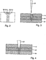
- the illustration of the Figure 1 schematically shows a sequence of a singulation method for singulating a semiconductor wafer comprising a plurality of solar cell stacks according to a first embodiment of the invention.
- a semiconductor wafer 10 comprising a plurality of solar cell stacks 12 and having an upper side 10.1 and a lower side 10.2 is provided.
- the semiconductor wafer 10 comprises a layer sequence composed of an underside 10.1 forming germanium substrate 14, a germanium partial cell 16, a first III-V partial cell 18 and a second III-V partial cell 20 forming the top 10.1.
- An adhesive layer 22 is on the top 10.1 and a cover glass layer 24 is on the adhesive layer 22 arranged.
- the solar cell stacks 12 of the semiconductor wafer 10 are separated along separating lines L.
- separating lines L For this purpose, by means of laser ablation with a laser moved along the separating lines L and a laser beam LS incident on the underside 10.2 of the semiconductor wafer, a laser beam LS is transmitted from the underside 10.2 through the substrate layer 14 and the sub-cells 16, 18, 20 of the semiconductor wafer 10 and through the adhesive layer 22 Trench G reaching into the cover glass layer 24 is produced.
- the trench G ends in a region of the cover glass layer 24 adjoining the adhesive layer 22, the region taking up a maximum of one third of the total thickness of the cover glass layer 24.
- the cover glass layer 24 is then divided along the dividing lines L by breaking or by sawing, as a result of which the solar cell stacks are separated from one another.
- the laser ablation takes place along the dividing line L and along four further tracks S1, S2, S4, S5 running parallel to the dividing line L.
- the laser ablation takes place in five passes, with the laser ablation taking place in a first pass along the dividing line and a further four tracks. In each subsequent pass, the laser ablation takes place with a lower focal plane and along a number of tracks reduced by one.
- Light diffracted by the exit surface of the cover glass layer 24 can, as in the case shown, strike the top side 10.1 of the semiconductor wafer 10 and damage the top side 10.1 of the semiconductor wafer 10.
- the intensity is greatly weakened, for example, when the laser beam LS has a large opening angle, i.e. when the laser beam expands quickly after the focal plane.
Landscapes
- Engineering & Computer Science (AREA)
- Physics & Mathematics (AREA)
- Optics & Photonics (AREA)
- Plasma & Fusion (AREA)
- Mechanical Engineering (AREA)
- Laser Beam Processing (AREA)
- Dicing (AREA)
- Life Sciences & Earth Sciences (AREA)
- Health & Medical Sciences (AREA)
- Molecular Biology (AREA)
- Sustainable Development (AREA)
- Sustainable Energy (AREA)
Description
- Die Erfindung betrifft ein Vereinzelungsverfahren zur Vereinzelung einer mehrere Solarzellenstapel umfassenden Halbleiterscheibe.
- Halbleiterscheiben (Wafer) werden typischerweise mittels eines Trennschleifprozesses vereinzelt, also mechanisch getrennt. Ebenfalls bekannt ist das Vereinzeln mittels Laser-Ablation entlang von Trennfugen.
- Alternativ werden in einem Ritzprozess d.h. in einem sogenannten Scribing Prozess mechanisch oder mittels Laser-Ablation kleine Gräben als Sollbruchstellen entlang von Trennlinien in der Oberseite oder der Unterseite erzeugt und die Halbleiterscheibe anschließend durch Brechen entlang der Sollbruchstellen geteilt.
- Ebenso ist es möglich mit einem sogenannten Stealth-Dicing Prozess, auch als verdeckte Vereinzelung bezeichnet, mittels eines In einer bestimmten Tiefe in der Halbleiterscheibe das Material zu modifizieren, wodurch ebenfalls Sollbruchstellen entstehen, entlang derer durch Brechen vereinzeln lässt.
- Die Vereinzelungsverfahren sind dabei jeweils an das zu teilende Material, also ein Halbleitermaterial angepasst.
- Aus der
US 2017/345955 A1 , und derUS 2018/097133 A1 , und derEP 0 926 743 A2 , und derEP 2 426 734 A2 , und aus DONGSHI ZHANG ET AL: "Debrisfree rear-side picosecond laser ablation of thin germanium wafers in water with ethanol", APPLIED SURFACE SCIENCE, Bd. 367, 12. Januar 2016, Seiten 222-230,US 2011/247672 A1 ,US 6 300 558 B1 sind Verfahren zum Vereinzein von Halbleiterscheiben bekannt. - Vor diesem Hintergrund besteht die Aufgabe der Erfindung darin, eine Vorrichtung anzugeben, die den Stand der Technik weiterbildet.
- Die Aufgabe wird durch ein Vereinzelungsverfahren mit den Merkmalen des Patentanspruchs 1 gelöst. Vorteilhafte Ausgestaltungen der Erfindung sind Gegenstand von Unteransprüchen.
- Gemäß dem Gegenstand der Erfindung wird ein Vereinzelungsverfahren zur Vereinzelung einer mehrere Solarzellenstapel umfassenden Halbleiterscheibe entlang mindestens einer Trennlinie bereitgestellt, mindestens umfassend die Schritte:
- Bereitstellen der Halbleiterscheibe mit einer Oberseite, einer Unterseite, einer mit der Oberseite stoffschlüssig verbundene Haftmittelschicht und eine stoffschlüssig mit der Haftmittelschicht verbundene Deckglasschicht, wobei die Halbleiterscheibe mehrere Solarzellenstapel jeweils aufweisend eine die Unterseite der Halbleiterscheibe ausbildende Germanium-Substratschicht, eine Germanium-Teilzelle und mindestens zwei III-V-Teilzellen umfasst,
- Erzeugen eines von einer Unterseite der Halbleiterscheibe durch die Halbleiterscheibe und die Haftmittelschicht hindurch mindestens bis zu einer an die Haftmittelschicht angrenzenden Unterseite der Deckglasschicht reichenden Trenngrabens entlang der Trennlinie mittels Laser-Ablation und
- Teilen der Deckglasschicht entlang des Trenngrabens.
- Es versteht sich, dass die einzelnen Teilzellen der Solarzellenstapel jeweils einen pn-Übergang aufweisen und die auf das Substrat folgenden Schichten epitaktisch aufeinander erzeugt und/oder mittels Wafer-Bond miteinander verbunden sind.
- Außerdem versteht es sich, dass eine Ge-Teilzelle Germanium aufweist oder aus Germanium besteht, wobei auch eine aus Germanium bestehende Schicht gegebenenfalls zusätzlich zu dem Germanium noch weitere Stoffe, insbesondere Dotierstoffe, aber auch Verunreinigungen enthält.
- Entsprechendes gilt auch für die III-V-Teilzellen, welche ein oder mehrere Materialien der III. sowie der V. Hauptgruppe aufweisen oder aus solchen Materialien bestehen.
- Ein mechanisches Trennen des Verbunds aus Halbleiterscheibe, Haftmittel und Deckglasschicht ist aufgrund der Härte des Glases und der zu erwartenden Ablagerungen des Haftmittels auf einer Trennscheibe nicht möglich.
- Dadurch dass der Trenngraben von der Unterseite der Halbleiterscheibe nur bis zu der Unterseite der Deckglasschicht oder einen an die Unterseite direkt angrenzenden Bereich der Deckglasschicht erzeugt wird, ist das Erzeugen des Trenngrabens trotz der sehr unterschiedlichen optischen und thermischen Eigenschaften möglich, insbesondere ohne die Haftmittelschicht unnötig zu beschädigen.
- Es versteht sich, dass der Trenngraben an der Unterseite der Halbleiterscheibe eine ausreichende Breite aufweisen muss, um den Laserstrahl für die Laser-Ablation bis zu der Deckglasschicht bis in ausreichende Tiefen fokussieren zu können. Andererseits fungiert der Trenngraben in der Halbleiterscheibe als Blende und verringert eine Rückstreuung von der Deckglasschicht in aktive Schichten der Halbleiterscheibe.
- Das Vereinzelungsverfahren ermöglicht es, den Verbund aus Halbleiterscheibe mit Haftmittel und Deckglas zu vereinzeln. Das Deckglas wird somit bereits auf Wafer-level aufgebracht und muss nur ein einziges Mal und nur verhältnismäßig grob justiert werden.
- Darüber hinaus stellt das Vereinzelungsverfahren sicher, dass das Deckglas mit den Seitenflächen der Halbleiterscheibe mindestens bündig abschließt oder sogar einen Überstand aufweist. Hierdurch ist die Oberseite der Halbleiterscheibe zuverlässig vor Umwelteinflüssen geschützt.
- Gemäß einer ersten Ausführungsform wird der Trenngraben bis in einen an die Haftmittelschicht angrenzenden Bereich der Deckglasschicht erzeugt wird. Die Laser-Ablation in einem unteren Bereich der Deckglasschicht stellt quasi einen Ritzprozess, auch Scribing genannt, dar. Durch das Anritzen der Deckglasschicht wird beispielsweise ein Brechen der Deckglasschicht entlang der Trenngräben vereinfacht.
- In einer anderen Ausführungsform erfolgt das Teilen der Deckglasschicht durch Brechen oder durch Sägen.
- Gemäß einer weiteren Ausführungsform wird für die Laser-Ablation ein Laser entlang mindestens einer entlang oder parallel zu der Trennlinie verlaufenden Spur auf der Unterseite der Halbleiterscheibe bewegt und erfolgen mittels eines fokussierten Laserstrahls Energieeinträge entlang der Spur.
- In einer Weiterbildung erfolgt der Energieeintrag entlang von mindestens 2 und höchstens 30 Spuren.
- Gemäß einer anderen Weiterbildung erfolgt in einem Ablations-Durchgang der Energieeintrag entlang von n Spuren mit 1 ≤ n ≤ 30 und der Ablations-Durchgang wird mindestens einmal wiederholt, wobei bei jeder Wiederholung die Anzahl n der Spuren gleich bleibt oder reduziert wird und wobei die Anzahl n bei mindestens einer Wiederholung reduziert wird.
- In einer weiteren Ausführungsform wird der Ablations-Durchgang mindestens einmal und höchstens 40 Mal wiederholt.
- Gemäß einer anderen Ausführungsform erfolgt in einem Ablations-Durchgang der Energieeintrag mit einer ersten Leistungsdichte und mit einer ersten Fokusebene und wird mindestens einmal wiederholt, wobei bei mindestens einer Wiederholung die Leistungsdichte und/oder die Fokusebene verändert wird.
- Gemäß einer weiteren Weiterbildung wird vor dem Erzeugen des Grabens die Oberseite der Deckglasschicht stoffschlüssig mit einer Folie verbunden.
- In einer anderen Weiterbildung umfasst die Haftmittelschicht Silikon und weist eine Dicke von mindestens 5µm auf.
- Gemäß einer weiteren Ausführungsform weist die Deckglasschicht eine Schichtdicke von mindestens 50 µm auf.
- In einer anderen Ausführungsform erfolgt der Energieeintrag mittels eines gepulsten Lasers, wobei eine Pulsdauer zwischen 10 fs und 100 ns beträgt und/oder eine Wellenlänge zwischen 315 nm und 1070 nm oder zwischen 1,5 µm und 10,6 µm beträgt.
- Die Erfindung wird nachfolgend unter Bezugnahme auf die Zeichnungen näher erläutert. Hierbei werden gleichartige Teile mit identischen Bezeichnungen beschriftet. Die dargestellten Ausführungsformen sind stark schematisiert, d.h. die Abstände und die laterale und die vertikale Erstreckung sind nicht maßstäblich und weisen, sofern nicht anders angegeben, auch keine ableitbaren geometrischen Relationen zueinander auf. Darin zeigt:
- Figur 1
- einen schematischen Ablauf gemäß einer ersten Ausführungsform eines erfindungsgemäßen Vereinzelungsverfahrens einer Halbleiterscheibe,
- Figur 2
- eine Ansicht einer zweite erfindungsgemäße Ausführungsform des Vereinzelungsverfahrens,
- Figur 3
- eine Ansicht einer weiteren erfindungsgemäßen Ausführungsform des Vereinzelungsverfahrens,
- Figur 4
- eine weitere Ansicht des Vereinzelungsverfahrens.
- Die Abbildung der
Figur 1 zeigt schematisch einen Ablauf eines Vereinzelungsverfahrens zur Vereinzelung einer mehrere Solarzellenstapel umfassenden Halbleiterscheibe gemäß einer ersten erfindungsgemäßen Ausführungsform. - Es wird eine mehrere Solarzellenstapel 12 umfassende Halbleiterscheibe 10 mit einer Oberseite 10.1 und einer Unterseite 10.2 bereitgestellt. Die Halbleiterscheibe 10 umfasst eine Schichtfolge aus einem die Unterseite 10.1 ausbildenden Germanium-Substrat 14, einer Germanium-Teilzelle 16, einer ersten III-V-Teilzelle 18 und einer die Oberseite 10.1 ausbildenden zweiten III-V-Teilzelle 20. Auf der Oberseite 10.1 ist eine Haftmittelschicht 22 und auf der Haftmittelschicht 22 eine Deckglasschicht 24 angeordnet.
- Die Solarzellenstapel 12 der Halbleiterscheibe 10 werden entlang von Trennlinien L vereinzelt. Hierfür wird mittels Laser-Ablation mit einem entlang der Trennlinien L bewegten Lasers und eines auf die Unterseite 10.2 der Halbleiterscheibe auftreffenden Laserstrahls LS ein von der Unterseite 10.2 durch die Substratschicht 14 und die Teilzellen 16, 18, 20 der Halbleiterscheibe 10 sowie durch die Haftmittelschicht 22 bis in die Deckglasschicht 24 hinein reichender Graben G erzeugt. Der Graben G endet in einem an die Haftmittelschicht 22 angrenzenden Bereich der Deckglasschicht 24, wobei der Bereich maximal ein Drittel der Gesamtdicke der Deckglasschicht 24 einnimmt.
- Anschließend wird die Deckglasschicht 24 entlang der Trennlinien L durch Brechen oder durch Sägen geteilt, wodurch die Solarzellenstapel voneinander getrennt werden.
- In der Abbildung der
Figur 2 ist eine weitere Ausführungsform dargestellt. Im Folgenden werden nur die Unterschiede zu der Abbildung derFigur 1 erläutert. - Um den Graben G entlang einer Trennlinie L zu erzeugen, erfolgt die Laser-Ablation entlang der Trennlinie L sowie entlang von vier weiteren parallel zu der Trennlinie L verlaufenden Spuren S1, S2, S4, S5 bewegt.
- In der Abbildung der
Figur 3 ist eine weitere Ausführungsform dargestellt. Im Folgenden werden nur die Unterschiede zu der Abbildung derFigur 2 erläutert. - Die Laser-Ablation erfolgt in fünf Durchgängen, wobei die Laser-Ablation in einem ersten Durchgang entlang der Trennlinie und weiterer vier Spuren erfolgt. In jedem weiteren Durchgang erfolgt die Laser-Ablation mit einer tiefer liegenden Fokusebene und entlang einer um eins verringerten Anzahl von Spuren.
- In der Abbildung der
Figur 3 ist ein Lichtverlauf durch die Halbleiterscheibe 10, die Haftmittelschicht 22 und der Deckglasschicht 24 dargestellt. - Von der Austrittfläche der Deckglasschicht 24 gebeugtes Licht kann, wie in dem dargestellten Fall, auf die Oberseite 10.1 der Halbleiterscheibe 10 treffen und die Oberseite 10.1 der Halbleiterscheibe 10 schädigen.
- Mit einer geeigneten Wahl der Energiedichte bzw. der Intensität und des Fokusverlaufs wird eine Schädigung unterdrückt oder zumindest reduziert.
- Insbesondere schwächt sich die Intensität beispielsweise stark ab, wenn der Laserstrahl LS einen großen Öffnungswinkel aufweist, d.h. wenn sich der Laserstrahl nach der Fokusebene also schnell aufweitet.
- Es sei angemerkt, dass sich bei der Bearbeitung mit einer größeren Rayleighlänge in Verbindung mit einer geeigneten Breite des Grabens G das Auftreffen von reflektiertem Licht auf der Oberseite 10.1 der Halbleiterscheibe 10 zuverlässig unterdrücken lässt.
Claims (12)
- Vereinzelungsverfahren zur Vereinzelung einer mehrere Solarzellenstapel (12) umfassenden Halbleiterscheibe (10) entlang mindestens einer Trennlinie (L) mindestens umfassend die Schritte:- Bereitstellen der Halbleiterscheibe (10) mit einer Oberseite (10.1), einer Unterseite (10.2), einer mit der Oberseite (10.1) stoffschlüssig verbundene Haftmittelschicht (22) und eine stoffschlüssig mit der Haftmittelschicht (22) verbundene Deckglasschicht (24),- wobei die Halbleiterscheibe (10) mehrere Solarzellenstapel (12) jeweils aufweisend eine die Unterseite (10.1) der Halbleiterscheibe (10) ausbildende Germanium-Substratschicht (14), eine Germanium-Teilzelle (16) und mindestens zwei III-V-Teilzellen (18, 20) umfasst,- Erzeugen eines von einer Unterseite (10.2) der Halbleiterscheibe (10) durch die Halbleiterscheibe (10) und die Haftmittelschicht (22) hindurch mindestens bis zu einer an die Haftmittelschicht (22) angrenzenden Unterseite der Deckglasschicht (24) reichenden Trenngrabens (G) entlang der Trennlinie (L) mittels Laser-Ablation und- Teilen der Deckglasschicht (24) entlang des Trenngrabens.
- Verfahren nach Anspruch 1, dadurch gekennzeichnet, dass der Trenngraben bis in einen an die Haftmittelschicht (22) angrenzenden Bereich der Deckglasschicht (24) erzeugt wird.
- Verfahren nach Anspruch 1 oder 2, dadurch gekennzeichnet, dass das Teilen der Deckglasschicht durch Brechen oder durch Sägen erfolgt.
- Verfahren nach einem der vorstehenden Ansprüche, dadurch gekennzeichnet, dass für die Laser-Ablation ein Laser (LA) entlang mindestens einer entlang oder parallel zu der Trennlinie (L) verlaufenden Spur (S1, S2, S4, S5) auf der Unterseite (10.2) der Halbleiterscheibe (10) bewegt wird und mittels eines fokussierten Laserstrahls (LS) Energieeinträge entlang der Spur erfolgen.
- Verfahren nach einem der vorstehenden Ansprüche, dadurch gekennzeichnet, dass der Energieeintrag entlang von mindestens 2 und höchstens 30 Spuren (S1, S2, S4, S5) erfolgt.
- Verfahren nach einem der vorstehenden Ansprüche, dadurch gekennzeichnet, dass in einem Ablations-Durchgang der Energieeintrag entlang von n Spuren (S1, S2, S4, S5) mit 1 ≤ n ≤ 30 erfolgt und der Ablations-Durchgang mindestens einmal wiederholt wird, wobei bei jeder Wiederholung die Anzahl n der Spuren gleich bleibt oder reduziert wird und wobei die Anzahl n bei mindestens einer Wiederholung reduziert wird.
- Verfahren nach Anspruch 6, dadurch gekennzeichnet, dass der Ablations-Durchgang mindestens einmal und höchstens 40 Mal wiederholt wird.
- Verfahren nach einem der vorstehenden Ansprüche, dadurch gekennzeichnet, dass in einem Ablations-Durchgang der Energieeintrag mit einer ersten Leistungsdichte und mit einer ersten Fokusebene erfolgt und der Ablations-Durchgang mindestens einmal wiederholt wird, wobei bei mindestens einer Wiederholung die Leistungsdichte und/oder die Fokusebene verändert wird.
- Verfahren nach einem der vorstehenden Ansprüche, dadurch gekennzeichnet, dass vor dem Erzeugen des Grabens die Oberseite der Deckglasschicht stoffschlüssig mit einer Folie verbunden wird.
- Verfahren nach einem der vorstehenden Ansprüche, dadurch gekennzeichnet, dass die Haftmittelschicht (22) Silikon umfasst und eine Dicke von mindestens 5 µm aufweist.
- Verfahren nach einem der vorstehenden Ansprüche, dadurch gekennzeichnet, dass die Deckglasschicht (24) eine Schichtdicke von mindestens 50 µm aufweist.
- Verfahren nach einem der vorstehenden Ansprüche, dadurch gekennzeichnet, dass der Energieeintrag mittels eines gepulsten Lasers (LA) erfolgt, wobei eine Pulsdauer zwischen 10 fs und 100 ns beträgt und/oder eine Wellenlänge zwischen 315 nm und 1070 nm oder zwischen 1,5 µm und 10,6 µm beträgt.
Applications Claiming Priority (1)
| Application Number | Priority Date | Filing Date | Title |
|---|---|---|---|
| DE102019006095.4A DE102019006095A1 (de) | 2019-08-29 | 2019-08-29 | Vereinzelungsverfahren zur Vereinzelung einer mehrere Solarzellenstapel umfasssenden Halbleiterscheibe |
Publications (2)
| Publication Number | Publication Date |
|---|---|
| EP3787044A1 EP3787044A1 (de) | 2021-03-03 |
| EP3787044B1 true EP3787044B1 (de) | 2021-08-04 |
Family
ID=72147857
Family Applications (1)
| Application Number | Title | Priority Date | Filing Date |
|---|---|---|---|
| EP20000294.7A Active EP3787044B1 (de) | 2019-08-29 | 2020-08-17 | Vereinzelungsverfahren zur vereinzelung einer mehrere solarzellenstapel umfassenden halbleiterscheibe |
Country Status (6)
| Country | Link |
|---|---|
| US (1) | US11380814B2 (de) |
| EP (1) | EP3787044B1 (de) |
| CN (1) | CN112447883B (de) |
| DE (1) | DE102019006095A1 (de) |
| ES (1) | ES2898334T3 (de) |
| RU (1) | RU2747424C9 (de) |
Families Citing this family (3)
| Publication number | Priority date | Publication date | Assignee | Title |
|---|---|---|---|---|
| CN114649199B (zh) * | 2022-03-14 | 2025-12-12 | 深圳先进电子材料国际创新研究院 | 一种激光解键合的方法及其应用 |
| US20240113072A1 (en) * | 2022-09-30 | 2024-04-04 | Intel Corporation | Singulation of integrated circuit package substrates with glass cores |
| DE102023002414A1 (de) * | 2023-06-14 | 2024-12-19 | Azur Space Solar Power Gmbh | Verfahren zur Herstellung eines Grabens bei einer III-V Mehrfachsolarzelle |
Family Cites Families (27)
| Publication number | Priority date | Publication date | Assignee | Title |
|---|---|---|---|---|
| KR100479962B1 (ko) * | 1996-02-09 | 2005-05-16 | 어드밴스드 레이저 세퍼래이션 인터내셔널 비.브이. | 반도체소자분리방법 |
| JP3516156B2 (ja) * | 1997-12-16 | 2004-04-05 | シャープ株式会社 | 太陽電池の製造方法および保護カバー用素材板 |
| US6331208B1 (en) * | 1998-05-15 | 2001-12-18 | Canon Kabushiki Kaisha | Process for producing solar cell, process for producing thin-film semiconductor, process for separating thin-film semiconductor, and process for forming semiconductor |
| JP3657143B2 (ja) * | 1999-04-27 | 2005-06-08 | シャープ株式会社 | 太陽電池及びその製造方法 |
| JP2001015786A (ja) * | 1999-07-02 | 2001-01-19 | Kanegafuchi Chem Ind Co Ltd | 集積型薄膜太陽電池の製造のためのレーザスクライブ法 |
| RU2244986C1 (ru) * | 2003-05-20 | 2005-01-20 | Открытое акционерное общество "Сатурн" | Способ изготовления фотопреобразователя |
| JP2008153349A (ja) * | 2006-12-15 | 2008-07-03 | Disco Abrasive Syst Ltd | ウェーハの分割方法 |
| DE102007060658A1 (de) * | 2007-12-15 | 2009-07-09 | Carl Baasel Lasertechnik Gmbh & Co. Kg | Verfahren zum Herstellen von Bauelementen und Einrichtung zum Durchführen des Verfahrens |
| GB2459274A (en) * | 2008-04-15 | 2009-10-21 | Renewable Energy Corp Asa | Wafer based solar panels |
| DE102008033352A1 (de) * | 2008-07-16 | 2010-01-21 | Concentrix Solar Gmbh | Solarzellenchips mit neuer Geometrie und Verfahren zu deren Herstellung |
| JP5048843B2 (ja) * | 2008-09-22 | 2012-10-17 | 株式会社アルバック | 太陽電池の製造方法 |
| JP5022341B2 (ja) * | 2008-11-19 | 2012-09-12 | 三菱重工業株式会社 | 光電変換装置 |
| DE102010005970A1 (de) * | 2010-01-28 | 2011-08-18 | SCHOTT Solar AG, 55122 | Verfahren zur Herstellung eines photovoltaischen Dünnschichtmoduls |
| JP2011198965A (ja) * | 2010-03-19 | 2011-10-06 | Fuji Electric Co Ltd | レーザースクライブ装置 |
| JP5231499B2 (ja) * | 2010-09-06 | 2013-07-10 | シャープ株式会社 | 太陽電池モジュール |
| WO2012147200A1 (ja) * | 2011-04-28 | 2012-11-01 | 三菱電機株式会社 | レーザ加工装置及び方法 |
| KR101244355B1 (ko) * | 2011-06-10 | 2013-03-18 | 주성엔지니어링(주) | 태양전지의 제조 방법 및 태양전지 생산 장비 |
| DE102013109478A1 (de) * | 2013-08-30 | 2015-03-05 | Hanergy Holding Group Ltd. | Verfahren zur Herstellung von Sub-Solarmodulen durch elektrisch isolierende Isoliergräben in einem Dünnschichtsolarmodul und Verfahren zur Herstellung eines Dünnschichtsolarmoduls mit derartigen Isoliergräben |
| KR101944657B1 (ko) | 2015-06-01 | 2019-01-31 | 에바나 테크놀로지스, 유에이비 | 분할된 레이저 빔들을 이용한 반도체 워크피스의 레이저 스크라이빙 방법 |
| ES2926948T3 (es) * | 2015-07-27 | 2022-10-31 | Sierra Space Corp | Sistema de matriz solar y método de fabricación |
| US9922895B2 (en) | 2016-05-05 | 2018-03-20 | Taiwan Semiconductor Manufacturing Company, Ltd. | Package with tilted interface between device die and encapsulating material |
| US9680035B1 (en) * | 2016-05-27 | 2017-06-13 | Solar Junction Corporation | Surface mount solar cell with integrated coverglass |
| CN105895745B (zh) * | 2016-06-21 | 2017-11-21 | 苏州协鑫集成科技工业应用研究院有限公司 | 异质结太阳能电池片的切割方法 |
| DE102016224978B4 (de) * | 2016-12-14 | 2022-12-29 | Disco Corporation | Substratbearbeitungsverfahren |
| RU2672760C1 (ru) * | 2018-01-09 | 2018-11-19 | Публичное акционерное общество "Сатурн" (ПАО "Сатурн") | Способ изготовления фотопреобразователя со встроенным диодом на германиевой подложке |
| FR3084203A1 (fr) * | 2018-07-20 | 2020-01-24 | Sunpartner Technologies | Procede industriel d'ablation laser de couches minces en une etape pour la realisation de modules photovoltaïques semi-transparents |
| KR102224624B1 (ko) * | 2019-02-27 | 2021-03-08 | 한국과학기술연구원 | 다중접합 태양전지 및 이의 제조방법 |
-
2019
- 2019-08-29 DE DE102019006095.4A patent/DE102019006095A1/de not_active Withdrawn
-
2020
- 2020-08-17 EP EP20000294.7A patent/EP3787044B1/de active Active
- 2020-08-17 ES ES20000294T patent/ES2898334T3/es active Active
- 2020-08-27 CN CN202010881681.2A patent/CN112447883B/zh active Active
- 2020-08-28 RU RU2020128657A patent/RU2747424C9/ru active
- 2020-08-31 US US17/007,676 patent/US11380814B2/en active Active
Also Published As
| Publication number | Publication date |
|---|---|
| EP3787044A1 (de) | 2021-03-03 |
| RU2747424C1 (ru) | 2021-05-04 |
| CN112447883B (zh) | 2023-07-14 |
| CN112447883A (zh) | 2021-03-05 |
| ES2898334T3 (es) | 2022-03-07 |
| DE102019006095A1 (de) | 2021-03-04 |
| US11380814B2 (en) | 2022-07-05 |
| US20210066533A1 (en) | 2021-03-04 |
| RU2747424C9 (ru) | 2022-01-17 |
Similar Documents
| Publication | Publication Date | Title |
|---|---|---|
| DE102004024643B4 (de) | Werkstückteilungsverfahren unter Verwendung eines Laserstrahls | |
| EP2509741B1 (de) | Verfahren und vorrichtung für ein laserabhebeverfahren mit einem strahlteiler | |
| DE102007010001B4 (de) | Verfahren zum Trennen von Wafern in Chips, sowie hiermit hergestellter Chip | |
| DE102013221822B4 (de) | Chip mit Rückseitenmetall und Verfahren zu seiner Herstellung und Halbleiterscheibe mit Rückseitenmetall | |
| EP1924392B1 (de) | Verfahren zum durchtrennen von spröden flachmaterialien mittels laser entlang einer zuvor erzeugten spur | |
| DE102014106472B4 (de) | Verfahren zum Strahlungsritzen eines Halbleitersubstrats | |
| DE112007001280T5 (de) | Waferritzen mit ultrakurzen Laserimpulsen | |
| DE102004055443A1 (de) | Waferbearbeitungsverfahren | |
| EP3787044A1 (de) | Vereinzelungsverfahren zur vereinzelung einer mehrere solarzellenstapel umfassenden halbleiterscheibe | |
| DE102014013107A1 (de) | Neuartiges Waferherstellungsverfahren | |
| DE112007001278T5 (de) | Infrarotlaser-Waferritzen unter Verwendung von kurzen Impulsen | |
| DE102006014852A1 (de) | Halbleiter-Wafer mit mehrfachen Halbleiterelementen und Verfahren zu ihrem Dicen | |
| EP2282969A2 (de) | Verfahren zur herstellung von vereinzelten, auf einem siliziumsubstrat angeordneten mikromechanischen bauteilen und hieraus hergestellte bauteile | |
| DE102013104270A1 (de) | Verfahren zur Herstellung eines optoelektronischen Halbleiterchips und optoelektronischer Halbleiterchip | |
| DE102019200462B4 (de) | Ausbilden von abschirmtunneln zum bearbeiten eines werkstücks mit einem laserstrahl | |
| DE102017106854B4 (de) | Trägeranordnung und Verfahren für die Bearbeitung eines Trägers | |
| WO2015027997A1 (de) | Verfahren zur laser-strukturierung von dünnschichten auf einem substrat für die herstellung monolithisch verschalteter dünnschichtsolarzellen und herstellungsverfahren für ein dünnschichtsolarmodul | |
| DE112016004420T5 (de) | Laserbearbeitungsverfahren und laserbearbeitungsvorrichtung | |
| EP1997137A1 (de) | Verfahren zum herstellen einer integrierten schaltung | |
| DE102014111977A1 (de) | Trennen von Chips auf einem Substrat | |
| DE112018003841T5 (de) | Schichtelement-herstellungsverfahren | |
| EP4388593A1 (de) | Verfahren zum vereinzeln von halbleiterbauelementen | |
| DE102020109149B4 (de) | Verfahren mit Stealth-Dicing-Prozess zur Herstellung von MEMS-Halbleiterchips | |
| DE102015004347A1 (de) | Erzeugung von physischen Modifikationen mittels LASER im Inneren eines Festkörpers | |
| DE102011011862A1 (de) | Verfahren zur Herstellung einer Vielzahl optoelektronischer Halbleiterchips |
Legal Events
| Date | Code | Title | Description |
|---|---|---|---|
| PUAI | Public reference made under article 153(3) epc to a published international application that has entered the european phase |
Free format text: ORIGINAL CODE: 0009012 |
|
| STAA | Information on the status of an ep patent application or granted ep patent |
Free format text: STATUS: THE APPLICATION HAS BEEN PUBLISHED |
|
| STAA | Information on the status of an ep patent application or granted ep patent |
Free format text: STATUS: REQUEST FOR EXAMINATION WAS MADE |
|
| AK | Designated contracting states |
Kind code of ref document: A1 Designated state(s): AL AT BE BG CH CY CZ DE DK EE ES FI FR GB GR HR HU IE IS IT LI LT LU LV MC MK MT NL NO PL PT RO RS SE SI SK SM TR |
|
| AX | Request for extension of the european patent |
Extension state: BA ME |
|
| 17P | Request for examination filed |
Effective date: 20210204 |
|
| RBV | Designated contracting states (corrected) |
Designated state(s): AL AT BE BG CH CY CZ DE DK EE ES FI FR GB GR HR HU IE IS IT LI LT LU LV MC MK MT NL NO PL PT RO RS SE SI SK SM TR |
|
| GRAP | Despatch of communication of intention to grant a patent |
Free format text: ORIGINAL CODE: EPIDOSNIGR1 |
|
| STAA | Information on the status of an ep patent application or granted ep patent |
Free format text: STATUS: GRANT OF PATENT IS INTENDED |
|
| INTG | Intention to grant announced |
Effective date: 20210503 |
|
| GRAS | Grant fee paid |
Free format text: ORIGINAL CODE: EPIDOSNIGR3 |
|
| GRAA | (expected) grant |
Free format text: ORIGINAL CODE: 0009210 |
|
| STAA | Information on the status of an ep patent application or granted ep patent |
Free format text: STATUS: THE PATENT HAS BEEN GRANTED |
|
| AK | Designated contracting states |
Kind code of ref document: B1 Designated state(s): AL AT BE BG CH CY CZ DE DK EE ES FI FR GB GR HR HU IE IS IT LI LT LU LV MC MK MT NL NO PL PT RO RS SE SI SK SM TR |
|
| REG | Reference to a national code |
Ref country code: GB Ref legal event code: FG4D Free format text: NOT ENGLISH |
|
| REG | Reference to a national code |
Ref country code: AT Ref legal event code: REF Ref document number: 1417892 Country of ref document: AT Kind code of ref document: T Effective date: 20210815 |
|
| REG | Reference to a national code |
Ref country code: CH Ref legal event code: EP |
|
| REG | Reference to a national code |
Ref country code: DE Ref legal event code: R096 Ref document number: 502020000111 Country of ref document: DE Ref country code: DE Ref legal event code: R083 Ref document number: 502020000111 Country of ref document: DE |
|
| REG | Reference to a national code |
Ref country code: NL Ref legal event code: FP |
|
| REG | Reference to a national code |
Ref country code: IE Ref legal event code: FG4D Free format text: LANGUAGE OF EP DOCUMENT: GERMAN |
|
| REG | Reference to a national code |
Ref country code: LT Ref legal event code: MG9D |
|
| PG25 | Lapsed in a contracting state [announced via postgrant information from national office to epo] |
Ref country code: SE Free format text: LAPSE BECAUSE OF FAILURE TO SUBMIT A TRANSLATION OF THE DESCRIPTION OR TO PAY THE FEE WITHIN THE PRESCRIBED TIME-LIMIT Effective date: 20210804 Ref country code: RS Free format text: LAPSE BECAUSE OF FAILURE TO SUBMIT A TRANSLATION OF THE DESCRIPTION OR TO PAY THE FEE WITHIN THE PRESCRIBED TIME-LIMIT Effective date: 20210804 Ref country code: HR Free format text: LAPSE BECAUSE OF FAILURE TO SUBMIT A TRANSLATION OF THE DESCRIPTION OR TO PAY THE FEE WITHIN THE PRESCRIBED TIME-LIMIT Effective date: 20210804 Ref country code: FI Free format text: LAPSE BECAUSE OF FAILURE TO SUBMIT A TRANSLATION OF THE DESCRIPTION OR TO PAY THE FEE WITHIN THE PRESCRIBED TIME-LIMIT Effective date: 20210804 Ref country code: NO Free format text: LAPSE BECAUSE OF FAILURE TO SUBMIT A TRANSLATION OF THE DESCRIPTION OR TO PAY THE FEE WITHIN THE PRESCRIBED TIME-LIMIT Effective date: 20211104 Ref country code: PT Free format text: LAPSE BECAUSE OF FAILURE TO SUBMIT A TRANSLATION OF THE DESCRIPTION OR TO PAY THE FEE WITHIN THE PRESCRIBED TIME-LIMIT Effective date: 20211206 Ref country code: LT Free format text: LAPSE BECAUSE OF FAILURE TO SUBMIT A TRANSLATION OF THE DESCRIPTION OR TO PAY THE FEE WITHIN THE PRESCRIBED TIME-LIMIT Effective date: 20210804 Ref country code: BG Free format text: LAPSE BECAUSE OF FAILURE TO SUBMIT A TRANSLATION OF THE DESCRIPTION OR TO PAY THE FEE WITHIN THE PRESCRIBED TIME-LIMIT Effective date: 20211104 |
|
| PG25 | Lapsed in a contracting state [announced via postgrant information from national office to epo] |
Ref country code: PL Free format text: LAPSE BECAUSE OF FAILURE TO SUBMIT A TRANSLATION OF THE DESCRIPTION OR TO PAY THE FEE WITHIN THE PRESCRIBED TIME-LIMIT Effective date: 20210804 Ref country code: LV Free format text: LAPSE BECAUSE OF FAILURE TO SUBMIT A TRANSLATION OF THE DESCRIPTION OR TO PAY THE FEE WITHIN THE PRESCRIBED TIME-LIMIT Effective date: 20210804 Ref country code: GR Free format text: LAPSE BECAUSE OF FAILURE TO SUBMIT A TRANSLATION OF THE DESCRIPTION OR TO PAY THE FEE WITHIN THE PRESCRIBED TIME-LIMIT Effective date: 20211105 |
|
| REG | Reference to a national code |
Ref country code: ES Ref legal event code: FG2A Ref document number: 2898334 Country of ref document: ES Kind code of ref document: T3 Effective date: 20220307 |
|
| PG25 | Lapsed in a contracting state [announced via postgrant information from national office to epo] |
Ref country code: DK Free format text: LAPSE BECAUSE OF FAILURE TO SUBMIT A TRANSLATION OF THE DESCRIPTION OR TO PAY THE FEE WITHIN THE PRESCRIBED TIME-LIMIT Effective date: 20210804 |
|
| REG | Reference to a national code |
Ref country code: DE Ref legal event code: R097 Ref document number: 502020000111 Country of ref document: DE |
|
| PG25 | Lapsed in a contracting state [announced via postgrant information from national office to epo] |
Ref country code: SM Free format text: LAPSE BECAUSE OF FAILURE TO SUBMIT A TRANSLATION OF THE DESCRIPTION OR TO PAY THE FEE WITHIN THE PRESCRIBED TIME-LIMIT Effective date: 20210804 Ref country code: SK Free format text: LAPSE BECAUSE OF FAILURE TO SUBMIT A TRANSLATION OF THE DESCRIPTION OR TO PAY THE FEE WITHIN THE PRESCRIBED TIME-LIMIT Effective date: 20210804 Ref country code: RO Free format text: LAPSE BECAUSE OF FAILURE TO SUBMIT A TRANSLATION OF THE DESCRIPTION OR TO PAY THE FEE WITHIN THE PRESCRIBED TIME-LIMIT Effective date: 20210804 Ref country code: MC Free format text: LAPSE BECAUSE OF FAILURE TO SUBMIT A TRANSLATION OF THE DESCRIPTION OR TO PAY THE FEE WITHIN THE PRESCRIBED TIME-LIMIT Effective date: 20210804 Ref country code: EE Free format text: LAPSE BECAUSE OF FAILURE TO SUBMIT A TRANSLATION OF THE DESCRIPTION OR TO PAY THE FEE WITHIN THE PRESCRIBED TIME-LIMIT Effective date: 20210804 Ref country code: CZ Free format text: LAPSE BECAUSE OF FAILURE TO SUBMIT A TRANSLATION OF THE DESCRIPTION OR TO PAY THE FEE WITHIN THE PRESCRIBED TIME-LIMIT Effective date: 20210804 Ref country code: AL Free format text: LAPSE BECAUSE OF FAILURE TO SUBMIT A TRANSLATION OF THE DESCRIPTION OR TO PAY THE FEE WITHIN THE PRESCRIBED TIME-LIMIT Effective date: 20210804 |
|
| PLBE | No opposition filed within time limit |
Free format text: ORIGINAL CODE: 0009261 |
|
| STAA | Information on the status of an ep patent application or granted ep patent |
Free format text: STATUS: NO OPPOSITION FILED WITHIN TIME LIMIT |
|
| 26N | No opposition filed |
Effective date: 20220506 |
|
| PG25 | Lapsed in a contracting state [announced via postgrant information from national office to epo] |
Ref country code: LU Free format text: LAPSE BECAUSE OF NON-PAYMENT OF DUE FEES Effective date: 20220817 |
|
| PG25 | Lapsed in a contracting state [announced via postgrant information from national office to epo] |
Ref country code: IE Free format text: LAPSE BECAUSE OF NON-PAYMENT OF DUE FEES Effective date: 20220817 Ref country code: HU Free format text: LAPSE BECAUSE OF FAILURE TO SUBMIT A TRANSLATION OF THE DESCRIPTION OR TO PAY THE FEE WITHIN THE PRESCRIBED TIME-LIMIT; INVALID AB INITIO Effective date: 20200817 |
|
| REG | Reference to a national code |
Ref country code: CH Ref legal event code: PL |
|
| PG25 | Lapsed in a contracting state [announced via postgrant information from national office to epo] |
Ref country code: CY Free format text: LAPSE BECAUSE OF FAILURE TO SUBMIT A TRANSLATION OF THE DESCRIPTION OR TO PAY THE FEE WITHIN THE PRESCRIBED TIME-LIMIT Effective date: 20210804 Ref country code: CH Free format text: LAPSE BECAUSE OF NON-PAYMENT OF DUE FEES Effective date: 20230831 |
|
| PG25 | Lapsed in a contracting state [announced via postgrant information from national office to epo] |
Ref country code: MK Free format text: LAPSE BECAUSE OF FAILURE TO SUBMIT A TRANSLATION OF THE DESCRIPTION OR TO PAY THE FEE WITHIN THE PRESCRIBED TIME-LIMIT Effective date: 20210804 |
|
| P01 | Opt-out of the competence of the unified patent court (upc) registered |
Free format text: CASE NUMBER: APP_40054/2024 Effective date: 20240704 |
|
| PG25 | Lapsed in a contracting state [announced via postgrant information from national office to epo] |
Ref country code: MT Free format text: LAPSE BECAUSE OF FAILURE TO SUBMIT A TRANSLATION OF THE DESCRIPTION OR TO PAY THE FEE WITHIN THE PRESCRIBED TIME-LIMIT Effective date: 20210804 |
|
| REG | Reference to a national code |
Ref country code: DE Ref legal event code: R079 Ref document number: 502020000111 Country of ref document: DE Free format text: PREVIOUS MAIN CLASS: H01L0031068700 Ipc: H10F0010142000 |
|
| PGFP | Annual fee paid to national office [announced via postgrant information from national office to epo] |
Ref country code: NL Payment date: 20250821 Year of fee payment: 6 |
|
| PGFP | Annual fee paid to national office [announced via postgrant information from national office to epo] |
Ref country code: ES Payment date: 20250926 Year of fee payment: 6 |
|
| PGFP | Annual fee paid to national office [announced via postgrant information from national office to epo] |
Ref country code: DE Payment date: 20250820 Year of fee payment: 6 |
|
| PGFP | Annual fee paid to national office [announced via postgrant information from national office to epo] |
Ref country code: IT Payment date: 20250825 Year of fee payment: 6 |
|
| PGFP | Annual fee paid to national office [announced via postgrant information from national office to epo] |
Ref country code: BE Payment date: 20250820 Year of fee payment: 6 Ref country code: GB Payment date: 20250820 Year of fee payment: 6 |
|
| PGFP | Annual fee paid to national office [announced via postgrant information from national office to epo] |
Ref country code: AT Payment date: 20251020 Year of fee payment: 5 Ref country code: FR Payment date: 20250828 Year of fee payment: 6 |
|
| PG25 | Lapsed in a contracting state [announced via postgrant information from national office to epo] |
Ref country code: TR Free format text: LAPSE BECAUSE OF FAILURE TO SUBMIT A TRANSLATION OF THE DESCRIPTION OR TO PAY THE FEE WITHIN THE PRESCRIBED TIME-LIMIT Effective date: 20210804 |
|
| PG25 | Lapsed in a contracting state [announced via postgrant information from national office to epo] |
Ref country code: SI Free format text: LAPSE BECAUSE OF FAILURE TO SUBMIT A TRANSLATION OF THE DESCRIPTION OR TO PAY THE FEE WITHIN THE PRESCRIBED TIME-LIMIT Effective date: 20210804 |